US6309465B1 - CVD reactor - Google Patents
CVD reactorDownload PDFInfo
- Publication number
- US6309465B1 US6309465B1US09/381,208US38120899AUS6309465B1US 6309465 B1US6309465 B1US 6309465B1US 38120899 AUS38120899 AUS 38120899AUS 6309465 B1US6309465 B1US 6309465B1
- Authority
- US
- United States
- Prior art keywords
- reactor according
- reactor
- hollow body
- susceptor
- cvd
- Prior art date
- Legal status (The legal status is an assumption and is not a legal conclusion. Google has not performed a legal analysis and makes no representation as to the accuracy of the status listed.)
- Expired - Lifetime
Links
- 235000012431wafersNutrition0.000claimsabstractdescription46
- 239000012530fluidSubstances0.000claimsabstractdescription33
- 230000005855radiationEffects0.000claimsabstractdescription6
- 239000007789gasSubstances0.000claimsdescription66
- 238000010438heat treatmentMethods0.000claimsdescription23
- 238000011010flushing procedureMethods0.000claimsdescription14
- 239000000463materialSubstances0.000claimsdescription9
- 239000000203mixtureSubstances0.000claimsdescription8
- 239000007788liquidSubstances0.000claimsdescription7
- XLYOFNOQVPJJNP-UHFFFAOYSA-NwaterSubstancesOXLYOFNOQVPJJNP-UHFFFAOYSA-N0.000claimsdescription6
- 229910052751metalInorganic materials0.000claimsdescription5
- 239000002184metalSubstances0.000claimsdescription5
- 239000010453quartzSubstances0.000claimsdescription4
- VYPSYNLAJGMNEJ-UHFFFAOYSA-Nsilicon dioxideInorganic materialsO=[Si]=OVYPSYNLAJGMNEJ-UHFFFAOYSA-N0.000claimsdescription4
- 229910052454barium strontium titanateInorganic materials0.000claimsdescription3
- 230000009977dual effectEffects0.000claimsdescription3
- 238000005530etchingMethods0.000claimsdescription3
- 230000017525heat dissipationEffects0.000claimsdescription3
- 238000004519manufacturing processMethods0.000claimsdescription3
- RTAQQCXQSZGOHL-UHFFFAOYSA-NTitaniumChemical compound[Ti]RTAQQCXQSZGOHL-UHFFFAOYSA-N0.000claimsdescription2
- VNSWULZVUKFJHK-UHFFFAOYSA-N[Sr].[Bi]Chemical compound[Sr].[Bi]VNSWULZVUKFJHK-UHFFFAOYSA-N0.000claimsdescription2
- 238000010521absorption reactionMethods0.000claimsdescription2
- 229910052788bariumInorganic materials0.000claimsdescription2
- DSAJWYNOEDNPEQ-UHFFFAOYSA-Nbarium atomChemical compound[Ba]DSAJWYNOEDNPEQ-UHFFFAOYSA-N0.000claimsdescription2
- 229910021523barium zirconateInorganic materials0.000claimsdescription2
- DQBAOWPVHRWLJC-UHFFFAOYSA-Nbarium(2+);dioxido(oxo)zirconiumChemical compound[Ba+2].[O-][Zr]([O-])=ODQBAOWPVHRWLJC-UHFFFAOYSA-N0.000claimsdescription2
- 239000011888foilSubstances0.000claimsdescription2
- 229910052712strontiumInorganic materials0.000claimsdescription2
- CIOAGBVUUVVLOB-UHFFFAOYSA-Nstrontium atomChemical compound[Sr]CIOAGBVUUVVLOB-UHFFFAOYSA-N0.000claimsdescription2
- VEALVRVVWBQVSL-UHFFFAOYSA-Nstrontium titanateChemical compound[Sr+2].[O-][Ti]([O-])=OVEALVRVVWBQVSL-UHFFFAOYSA-N0.000claimsdescription2
- 238000001816coolingMethods0.000claims1
- 229910052451lead zirconate titanateInorganic materials0.000claims1
- HFGPZNIAWCZYJU-UHFFFAOYSA-Nlead zirconate titanateChemical compound[O-2].[O-2].[O-2].[O-2].[O-2].[Ti+4].[Zr+4].[Pb+2]HFGPZNIAWCZYJU-UHFFFAOYSA-N0.000claims1
- 150000002739metalsChemical class0.000claims1
- 238000000034methodMethods0.000description4
- 230000008901benefitEffects0.000description3
- 238000006243chemical reactionMethods0.000description3
- 239000000498cooling waterSubstances0.000description3
- 230000008569processEffects0.000description3
- IJGRMHOSHXDMSA-UHFFFAOYSA-NAtomic nitrogenChemical compoundN#NIJGRMHOSHXDMSA-UHFFFAOYSA-N0.000description2
- 230000035508accumulationEffects0.000description2
- 238000009825accumulationMethods0.000description2
- UFHFLCQGNIYNRP-UHFFFAOYSA-NHydrogenChemical compound[H][H]UFHFLCQGNIYNRP-UHFFFAOYSA-N0.000description1
- 230000009471actionEffects0.000description1
- 239000000443aerosolSubstances0.000description1
- 239000012159carrier gasSubstances0.000description1
- 239000003795chemical substances by applicationSubstances0.000description1
- 238000004140cleaningMethods0.000description1
- 239000011248coating agentSubstances0.000description1
- 238000000576coating methodMethods0.000description1
- 238000009826distributionMethods0.000description1
- 239000001257hydrogenSubstances0.000description1
- 229910052739hydrogenInorganic materials0.000description1
- 238000002488metal-organic chemical vapour depositionMethods0.000description1
- 238000012986modificationMethods0.000description1
- 230000004048modificationEffects0.000description1
- 229910052757nitrogenInorganic materials0.000description1
- 230000003071parasitic effectEffects0.000description1
- 239000012495reaction gasSubstances0.000description1
- 239000000243solutionSubstances0.000description1
- 239000007921spraySubstances0.000description1
Images
Classifications
- C—CHEMISTRY; METALLURGY
- C23—COATING METALLIC MATERIAL; COATING MATERIAL WITH METALLIC MATERIAL; CHEMICAL SURFACE TREATMENT; DIFFUSION TREATMENT OF METALLIC MATERIAL; COATING BY VACUUM EVAPORATION, BY SPUTTERING, BY ION IMPLANTATION OR BY CHEMICAL VAPOUR DEPOSITION, IN GENERAL; INHIBITING CORROSION OF METALLIC MATERIAL OR INCRUSTATION IN GENERAL
- C23C—COATING METALLIC MATERIAL; COATING MATERIAL WITH METALLIC MATERIAL; SURFACE TREATMENT OF METALLIC MATERIAL BY DIFFUSION INTO THE SURFACE, BY CHEMICAL CONVERSION OR SUBSTITUTION; COATING BY VACUUM EVAPORATION, BY SPUTTERING, BY ION IMPLANTATION OR BY CHEMICAL VAPOUR DEPOSITION, IN GENERAL
- C23C16/00—Chemical coating by decomposition of gaseous compounds, without leaving reaction products of surface material in the coating, i.e. chemical vapour deposition [CVD] processes
- C23C16/44—Chemical coating by decomposition of gaseous compounds, without leaving reaction products of surface material in the coating, i.e. chemical vapour deposition [CVD] processes characterised by the method of coating
- C23C16/455—Chemical coating by decomposition of gaseous compounds, without leaving reaction products of surface material in the coating, i.e. chemical vapour deposition [CVD] processes characterised by the method of coating characterised by the method used for introducing gases into reaction chamber or for modifying gas flows in reaction chamber
- C23C16/45563—Gas nozzles
- C23C16/45565—Shower nozzles
- C—CHEMISTRY; METALLURGY
- C23—COATING METALLIC MATERIAL; COATING MATERIAL WITH METALLIC MATERIAL; CHEMICAL SURFACE TREATMENT; DIFFUSION TREATMENT OF METALLIC MATERIAL; COATING BY VACUUM EVAPORATION, BY SPUTTERING, BY ION IMPLANTATION OR BY CHEMICAL VAPOUR DEPOSITION, IN GENERAL; INHIBITING CORROSION OF METALLIC MATERIAL OR INCRUSTATION IN GENERAL
- C23C—COATING METALLIC MATERIAL; COATING MATERIAL WITH METALLIC MATERIAL; SURFACE TREATMENT OF METALLIC MATERIAL BY DIFFUSION INTO THE SURFACE, BY CHEMICAL CONVERSION OR SUBSTITUTION; COATING BY VACUUM EVAPORATION, BY SPUTTERING, BY ION IMPLANTATION OR BY CHEMICAL VAPOUR DEPOSITION, IN GENERAL
- C23C16/00—Chemical coating by decomposition of gaseous compounds, without leaving reaction products of surface material in the coating, i.e. chemical vapour deposition [CVD] processes
- C23C16/44—Chemical coating by decomposition of gaseous compounds, without leaving reaction products of surface material in the coating, i.e. chemical vapour deposition [CVD] processes characterised by the method of coating
- C23C16/4412—Details relating to the exhausts, e.g. pumps, filters, scrubbers, particle traps
- C—CHEMISTRY; METALLURGY
- C23—COATING METALLIC MATERIAL; COATING MATERIAL WITH METALLIC MATERIAL; CHEMICAL SURFACE TREATMENT; DIFFUSION TREATMENT OF METALLIC MATERIAL; COATING BY VACUUM EVAPORATION, BY SPUTTERING, BY ION IMPLANTATION OR BY CHEMICAL VAPOUR DEPOSITION, IN GENERAL; INHIBITING CORROSION OF METALLIC MATERIAL OR INCRUSTATION IN GENERAL
- C23C—COATING METALLIC MATERIAL; COATING MATERIAL WITH METALLIC MATERIAL; SURFACE TREATMENT OF METALLIC MATERIAL BY DIFFUSION INTO THE SURFACE, BY CHEMICAL CONVERSION OR SUBSTITUTION; COATING BY VACUUM EVAPORATION, BY SPUTTERING, BY ION IMPLANTATION OR BY CHEMICAL VAPOUR DEPOSITION, IN GENERAL
- C23C16/00—Chemical coating by decomposition of gaseous compounds, without leaving reaction products of surface material in the coating, i.e. chemical vapour deposition [CVD] processes
- C23C16/44—Chemical coating by decomposition of gaseous compounds, without leaving reaction products of surface material in the coating, i.e. chemical vapour deposition [CVD] processes characterised by the method of coating
- C23C16/455—Chemical coating by decomposition of gaseous compounds, without leaving reaction products of surface material in the coating, i.e. chemical vapour deposition [CVD] processes characterised by the method of coating characterised by the method used for introducing gases into reaction chamber or for modifying gas flows in reaction chamber
Definitions
- the present inventionrelates to a CVD reactor in accordance with the introductory clause the Patent Claim 1, as well as to its application.
- CVD reactorsare generally common and are manufactured and distributed by companies such as Aixtron AG, Aachen, Germany. For an explanation of all terms which are not described here in more details explicit reference is made to these known CVD reactors.
- the known CVD reactorscomprise a reactor casing with a cover, in which a heated susceptor (wafer carrier) is provided on which at least one wafer can be positioned.
- a central fluid inletis provided as a rule for the supply of CVD gases or liquids.
- the fluid outletis then arranged mostly on the periphery of the reactor casing.
- Either central gas inlet nozzles, which permit the radial outflow of the gases from the centre of the reactor via the wafers, or so-called shower headsare used in or on the reactor cover, which are disposed directly above the wafer and spray the gas in the form of a shower through a great number of small holes in a vertical downward direction onto the wafers.
- Such reactorsare distributed, for instance, by the company of Thomas Swan, GB.
- German Patent DE 43 30 266discloses a similar structure, wherein a single-wafer reaction chamber includes a wafer heating stage for holding a wafer down and for heating the wafer. Moreover, a gas supply head including gas inlet nozzles is located opposite to the wafer heating stage so that a zone of constant spacing is created for the supply of reaction gas. Gases are then allowed to flow out via the gas supply head. An exhaust gas outlet is equally provided.
- the present inventionis based on the problem of improving a CVD reactor comprising a fluid inlet configured as shower head or gas inlet nozzles in such a way that the fluid inlet and hence the fluids to be introduced, i.e. gases and/or liquids, can be moderately heated in a simple manner and particularly with water passages etc. being dispensed with.
- Patent Claim 1One inventive solution to this problem is defined in Patent Claim 1. Improvements of the invention are the subject matters of Claims 2 et seq. In Claims 31 and 32 methods using a reactor defined in accordance with the invention are claimed.
- the fluid inlet unitcomprises a hollow body spaced from the reactor cover, with the underside of the hollow body, in which the openings are provided, being heated substantially by thermal radiation from the susceptor (wafer carrier),
- a flushing gas inlet devicewhich introduces a flushing gas into the space between the upper side of the hollow body and the reactor cover in such a way that the upper side radiates heat substantially by thermal convection in the gas to the environment, and
- CVD mediais to be understood to denote CVD and particularly MOCVD gases, liquids, solutions or mixture of the aforementioned substances—which will also be generally referred to in the following by the general term “fluid”.
- the fluid inlet unitcomprises a unit which has roughly the shape of a hollow disk with a plurality of outlet openings for the CVD media, etc.—i.e. of a shower head known per se—and is disposed between the susceptor (wafer carrier) and the reactor cover in such a way that the underside of the fluid inlet unit is heated by radiation from the susceptor (wafer carrier) and is hence adjusted to be a temperature between the temperature of the susceptor (wafer carrier) and the reactor cover so that the CVD media etc. will be moderately heated when they pass through the fluid inlet unit.
- an (adjustable) heat sinkis provided on the upper side of the fluid inlet unit a defined temperature gradient is created in the axial direction via the fluid inlet unit.
- the inventionstarts out from the fundamental idea to simplify the complex structure of known reactors in which the adjustment of the reactor cover and of the gas inlet in the form of a shower head through which a liquid passes and of separate heating systems required to this end is performed under thermostat control, by the provision that the shower head is configured as a component separate from the reactor cover.
- the susceptorwafer carrier
- the susceptoris heated any how by an infrared heating, a resistance heating or a high-frequency heating to a temperature level between roughly RT° C. and 1200° C. in a typical case (RT denotes room temperature) and hence radiates a substantial heat quantity to its environment by radiation
- the fluid inlet unitis heated.
- the temperature to which the fluid inlet unit is heatedis set in a controlled manner.
- a thin shower head made of a metal having good heat conduction propertiesin the reactor below the reactor cover and possibly underneath a ceiling under the thermostat control.
- the shower headis heated directly by the radiation from below from the susceptor (wafer carrier).
- the spacing between the susceptor (wafer carrier) and the hollow bodymay be adjustable for setting the temperature of the underside of the hollow body.
- a holding unitmay be provided for the hollow body with a thread.
- the heat supply or dissipation to or from the hollow bodyis determined by the temperature of the susceptor (wafer carrier), by the spacing from the susceptor (wafer carrier) which can now be freely adjusted, and by the conductivity of the gas in the reactor (selection of the carrier gas, e.g. nitrogen or hydrogen or a mixture of these gases and total pressure).
- selection of the carrier gase.g. nitrogen or hydrogen or a mixture of these gases and total pressure.
- the heat dissipation from the upper side of the shower heat in an upward directionis determined by the particular flushing gas which is used above the shower head and the quartz ceiling, and by the particular flushing gas used between the quartz ceiling and the cover of the metal reactor.
- thermostatically controlled ceilingproposed by Frijlink et al. may be employed in particular.
- the application of two flushing gas mixturespermits a highly precise control or setting of the absolute temperature and of the temperature gradient of the shower head in the reactor.
- the temperature gradientmay be additionally influenced in a controlled manner by means of a further embodiment providing for the introduction of local metal sheets serving as thermal shields and a multi-layer configuration of the shower head with materials presenting different coefficients of reflection and absorption.
- the reactorpresents a conventional structure: in particular, the reactor may be a round reactor—resembling the known planetary reactor—with a central gas inlet and a gas outlet (exhaust) surrounding it on the outside.
- the gas outlet (exhaust)may be the tunnel, in particular, which has been proposed by Frijlink et al.
- the ceiling of the reactormay equally be configured in the form proposed by Frijlink and is hence adapted for thermostatic control.
- the susceptoris either a planetary susceptor (planetary wafer carrier) with dual rotation or only a large plain disk which, however, operates also on gas foil rotation (i.e. rotation of the wafers on a gas cushion; patent held by the Applicant, the company of Aixtron) or which is mechanically rotated. In the latter case, one wafer can be centrally positioned for each process only but this wafer may have major dimensions. In an alternative or additionally it is possible to rotate the fluid inlet device about its axial axis.
- ⁇ -diketonates or other metal-organic solutionsare used which may be mixed, on the one hand, in the shower head directly by the structural provision of one or several inlets into the shower head, at the same temperature or at different temperature levels.
- the shower headmay also by configured in such a way that different gases are separately passed in the shower head and that they are thoroughly mixed only when they leave the shower head into the reactor space so as to avoid parasitic pre-reactions.
- the shower headis substantially easier to adjust and exchange.
- the reactorbecomes highly flexible because the most different shower heads can be mounted and exchanged very quickly for adjustment to different wafer sizes, without any major modifications of the reactor, dismantling or opening of medium-carrying lines.
- the reactoris thermally defined on all sides and all the walls are heated so that a minimum of accumulations will be created.
- the inventive reactormay be used for CVD processes of any kind, hence, for instance, for the application or processing of III-V, II-VI, IV-IV materials, moreover of single-component or multi-component oxides, perovskites such as barium and strontium titanate (ST or BT, respectively), barium strontium titanate (BST), strontium and barium zirconate titanates, strontium bismuth tantalate (SBT), lead circonate titanate (PZT) as well as the aforementioned material systems doped with an acceptor or/and a donator.
- perovskitessuch as barium and strontium titanate (ST or BT, respectively), barium strontium titanate (BST), strontium and barium zirconate titanates, strontium bismuth tantalate (SBT), lead circonate titanate (PZT) as well as the aforementioned material systems doped with an acceptor or/and a donator.
- shower headsare very easy to exchange. In dependence on the respective wafer shape used, it is thus possible to use shower heads having an arrangement of holes or outlets in correspondence with the arrangement and the shape of the wafers disposed therebeneath so that a highly homogeneous and yet economical processing or coating of the wafers will be possible.
- the reactor presenting the inventive designmay also be operated with etching or cleansing fluids so as to remove possibly created accumulations or condensates as rapidly as possible (self cleaning).
- the reactoris equipped with a shower head made of a material resistant to the etching gas.
- the reactormay be operated on a normal gas supply system or even with a source distribution system (liquid delivery system) or an aerosol system which supplies the gases in a moderately heated state already (so-called LDS system).
- a source distribution systemliquid delivery system
- an aerosol systemwhich supplies the gases in a moderately heated state already (so-called LDS system).
- the most different rotational speedsmay be used in the range from 5 to 1500 revolutions per minute (rpm).
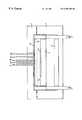
- FIGUREshows a schematic cross-sectional view taken through an inventive device.
- the CVD reactor illustrated in the cross-sectional view in the FIGUREcomprises a reactor vessel 1 with reactor cover 2 .
- the reactor vessel 1 and the cover 2are water-cooled so that they are permanently maintained approximately at room temperature.
- a gas outlet 21is provided in a manner known per se.
- a susceptor (wafer carrier) 3 for wafers 4is disposed which are to be processed or coated, respectively, by means of a CVD process.
- the susceptor (wafer carrier) 3is heated to a temperature between roughly RT° C. and 1200° C. (RT means room temperature) by means of a heating means 5 which may be of the infrared, the resistance or the high-frequency type.
- a fluid inlet unit 6is disposed above the susceptor (wafer carrier) 3 which, in the embodiment illustrated here, has the shape of a hollow disk.
- a plurality of holes(schematically indicated in the FIGURE) is provided in the underside 6 ′ of the unit 6 in an arrangement which may be matched with the shape of the wafer 4 .
- the spacing between the fluid inlet unit 6 and the susceptor (wafer carrier) 3may be adjusted by means such as a threading.
- Lines 71 and 73open into the interior space of the hollow disk 6 , through which the gases and particularly CVD gases flow from a gas supply unit—which is not illustrated here but is known per se in all respects and which includes a means for moderate pre-heating if necessary—into the interior space of the hollow disk 6 .
- the gasesthen leave the interior space through the holes (not illustrated here) and produce a homogeneous action upon the wafers 4 .
- a thermal shield 8which is also referred to as ceiling, is provided between the hollow disk 6 and the underside of the reactor cover 2 .
- the thermal shield 8is a plate made of a thermally resistant and inert material; in the embodiment illustrated here the plate is made of quartz.
- a flushing gas inlet meansis provided which is connected to the reactor via lines 91 and 92 .
- the line 91opens into the space between the thermal shield 8 and the upper side of the hollow disk 6 whereas the line 92 opens into the space between the reactor cover 2 and the thermal shield 8 .
- the flushing gas inlet meansis so configured that the composition and/or the flow rate of the gases introduced into the space or spaces above the upper side of the hollow body may be varied for setting the conditions of heat dissipation.
- the conditions of heat supply and dissipation to or from the hollow body 6may be so controlled that the lower side adjusts itself to a selectable temperature, by which the CVD media undergo a moderate heating, without the supply of a medium for moderate heating from the outside, and that a positive temperature gradient will occur between the upper side and the underside of the hollow body. With these provisions clogging of the holes is avoided. Moreover, a positive temperature gradient towards the susceptor (wafer carrier) prevails.
Landscapes
- Chemical & Material Sciences (AREA)
- General Chemical & Material Sciences (AREA)
- Chemical Kinetics & Catalysis (AREA)
- Engineering & Computer Science (AREA)
- Materials Engineering (AREA)
- Mechanical Engineering (AREA)
- Metallurgy (AREA)
- Organic Chemistry (AREA)
- Chemical Vapour Deposition (AREA)
Abstract
Description
Claims (32)
Applications Claiming Priority (1)
| Application Number | Priority Date | Filing Date | Title |
|---|---|---|---|
| PCT/DE1999/000455WO1999042636A1 (en) | 1998-02-18 | 1999-02-18 | Cvd reactor and use thereof |
Publications (1)
| Publication Number | Publication Date |
|---|---|
| US6309465B1true US6309465B1 (en) | 2001-10-30 |
Family
ID=6918809
Family Applications (1)
| Application Number | Title | Priority Date | Filing Date |
|---|---|---|---|
| US09/381,208Expired - LifetimeUS6309465B1 (en) | 1999-02-18 | 1999-02-18 | CVD reactor |
Country Status (1)
| Country | Link |
|---|---|
| US (1) | US6309465B1 (en) |
Cited By (31)
| Publication number | Priority date | Publication date | Assignee | Title |
|---|---|---|---|---|
| US20020166507A1 (en)* | 1999-03-12 | 2002-11-14 | Tokyo Electron Limited | Thin film forming apparatus |
| US20030054099A1 (en)* | 2000-02-16 | 2003-03-20 | Holger Jurgensen | Condensation coating process |
| US20030180460A1 (en)* | 2000-09-22 | 2003-09-25 | Gerd Strauch | Method for depositing in particular crystalline layers, gas-admission element and device for carrying out the method |
| US20040200407A1 (en)* | 2003-04-11 | 2004-10-14 | Frank Reinhardt | Low indium content quantum well structures |
| US20070234956A1 (en)* | 2006-04-05 | 2007-10-11 | Dalton Jeremie J | Method and apparatus for providing uniform gas delivery to a reactor |
| US20070256635A1 (en)* | 2006-05-02 | 2007-11-08 | Applied Materials, Inc. A Delaware Corporation | UV activation of NH3 for III-N deposition |
| WO2009048490A1 (en)* | 2007-10-10 | 2009-04-16 | Michael Iza | Chemical vapor deposition reactor chamber |
| US20090149008A1 (en)* | 2007-10-05 | 2009-06-11 | Applied Materials, Inc. | Method for depositing group iii/v compounds |
| US20090194026A1 (en)* | 2008-01-31 | 2009-08-06 | Burrows Brian H | Processing system for fabricating compound nitride semiconductor devices |
| US20090211707A1 (en)* | 2008-02-22 | 2009-08-27 | Hermes Systems Inc. | Apparatus for gas distribution and its applications |
| US20100111650A1 (en)* | 2008-01-31 | 2010-05-06 | Applied Materials, Inc. | Automatic substrate loading station |
| US20100215854A1 (en)* | 2007-06-24 | 2010-08-26 | Burrows Brian H | Hvpe showerhead design |
| US20100258049A1 (en)* | 2009-04-10 | 2010-10-14 | Applied Materials, Inc. | Hvpe chamber hardware |
| US20100273318A1 (en)* | 2009-04-24 | 2010-10-28 | Applied Materials, Inc. | Substrate pretreatment for subsequent high temperature group iii depositions |
| US20100273290A1 (en)* | 2009-04-28 | 2010-10-28 | Applied Materials, Inc. | Mocvd single chamber split process for led manufacturing |
| US20100279020A1 (en)* | 2009-04-29 | 2010-11-04 | Applied Materials, Inc. | METHOD OF FORMING IN-SITU PRE-GaN DEPOSITION LAYER IN HVPE |
| US20110070721A1 (en)* | 2006-04-14 | 2011-03-24 | Applied Materials, Inc. | Epitaxial growth of compound nitride semiconductor structures |
| US20110114020A1 (en)* | 2001-07-16 | 2011-05-19 | Gwo-Chuan Tzu | Lid assembly for a processing system to facilitate sequential deposition techniques |
| US20110155061A1 (en)* | 2009-12-31 | 2011-06-30 | National Chiao Tung University | Reactor, chemical vapor deposition reactor, and metalorganic chemical vapor deposition reactor |
| US8183132B2 (en) | 2009-04-10 | 2012-05-22 | Applied Materials, Inc. | Methods for fabricating group III nitride structures with a cluster tool |
| US8361892B2 (en) | 2010-04-14 | 2013-01-29 | Applied Materials, Inc. | Multiple precursor showerhead with by-pass ports |
| US8778079B2 (en) | 2007-10-11 | 2014-07-15 | Valence Process Equipment, Inc. | Chemical vapor deposition reactor |
| US9057128B2 (en) | 2011-03-18 | 2015-06-16 | Applied Materials, Inc. | Multiple level showerhead design |
| US9076827B2 (en) | 2010-09-14 | 2015-07-07 | Applied Materials, Inc. | Transfer chamber metrology for improved device yield |
| US20160027674A1 (en)* | 2013-03-15 | 2016-01-28 | Kevin Griffin | Carousel Gas Distribution Assembly With Optical Measurements |
| US9340875B2 (en) | 2013-06-17 | 2016-05-17 | Industrial Technology Research Institute | Reaction device with peripheral-in and center-out design for chemical vapor deposition |
| US9427762B2 (en) | 2013-02-23 | 2016-08-30 | Hermes-Epitek Corporation | Gas injector and cover plate assembly for semiconductor equipment |
| CN114144540A (en)* | 2019-07-26 | 2022-03-04 | 应用材料公司 | Evaporator chamber for forming a film on a substrate |
| US11534790B2 (en) | 2017-04-10 | 2022-12-27 | Samsung Display Co., Ltd. | Apparatus and method of manufacturing display apparatus |
| WO2023140824A3 (en)* | 2022-01-24 | 2023-08-24 | Tobb Ekonomi Ve Teknoloji Universitesi | A reactor |
| US12322644B2 (en) | 2020-09-03 | 2025-06-03 | Veeco Instruments, Inc. | Reactor with centering pin for epitaxial deposition |
Citations (3)
| Publication number | Priority date | Publication date | Assignee | Title |
|---|---|---|---|---|
| US5755886A (en)* | 1986-12-19 | 1998-05-26 | Applied Materials, Inc. | Apparatus for preventing deposition gases from contacting a selected region of a substrate during deposition processing |
| US5766364A (en)* | 1996-07-17 | 1998-06-16 | Matsushita Electric Industrial Co., Ltd. | Plasma processing apparatus |
| US6055927A (en)* | 1997-01-14 | 2000-05-02 | Applied Komatsu Technology, Inc. | Apparatus and method for white powder reduction in silicon nitride deposition using remote plasma source cleaning technology |
- 1999
- 1999-02-18USUS09/381,208patent/US6309465B1/ennot_activeExpired - Lifetime
Patent Citations (3)
| Publication number | Priority date | Publication date | Assignee | Title |
|---|---|---|---|---|
| US5755886A (en)* | 1986-12-19 | 1998-05-26 | Applied Materials, Inc. | Apparatus for preventing deposition gases from contacting a selected region of a substrate during deposition processing |
| US5766364A (en)* | 1996-07-17 | 1998-06-16 | Matsushita Electric Industrial Co., Ltd. | Plasma processing apparatus |
| US6055927A (en)* | 1997-01-14 | 2000-05-02 | Applied Komatsu Technology, Inc. | Apparatus and method for white powder reduction in silicon nitride deposition using remote plasma source cleaning technology |
Cited By (49)
| Publication number | Priority date | Publication date | Assignee | Title |
|---|---|---|---|---|
| US6866882B1 (en)* | 1999-03-12 | 2005-03-15 | Tokyo Electron Limited | Method of forming a thin film |
| US20020166507A1 (en)* | 1999-03-12 | 2002-11-14 | Tokyo Electron Limited | Thin film forming apparatus |
| US7201942B2 (en)* | 2000-02-16 | 2007-04-10 | Aixtron Ag | Coating method |
| US20030054099A1 (en)* | 2000-02-16 | 2003-03-20 | Holger Jurgensen | Condensation coating process |
| US20030180460A1 (en)* | 2000-09-22 | 2003-09-25 | Gerd Strauch | Method for depositing in particular crystalline layers, gas-admission element and device for carrying out the method |
| US6786973B2 (en)* | 2000-09-22 | 2004-09-07 | Aixtron Ag | Method for depositing in particular crystalline layers, gas-admission element and device for carrying out the method |
| US20110114020A1 (en)* | 2001-07-16 | 2011-05-19 | Gwo-Chuan Tzu | Lid assembly for a processing system to facilitate sequential deposition techniques |
| US20040200407A1 (en)* | 2003-04-11 | 2004-10-14 | Frank Reinhardt | Low indium content quantum well structures |
| US6936103B2 (en) | 2003-04-11 | 2005-08-30 | Spectra-Physics, Inc. | Low indium content quantum well structures |
| US20070234956A1 (en)* | 2006-04-05 | 2007-10-11 | Dalton Jeremie J | Method and apparatus for providing uniform gas delivery to a reactor |
| US20090324829A1 (en)* | 2006-04-05 | 2009-12-31 | Dalton Jeremie J | Method and apparatus for providing uniform gas delivery to a reactor |
| US7981472B2 (en) | 2006-04-05 | 2011-07-19 | Aixtron, Inc. | Methods of providing uniform gas delivery to a reactor |
| US20110070721A1 (en)* | 2006-04-14 | 2011-03-24 | Applied Materials, Inc. | Epitaxial growth of compound nitride semiconductor structures |
| US20070256635A1 (en)* | 2006-05-02 | 2007-11-08 | Applied Materials, Inc. A Delaware Corporation | UV activation of NH3 for III-N deposition |
| US20100215854A1 (en)* | 2007-06-24 | 2010-08-26 | Burrows Brian H | Hvpe showerhead design |
| US20090149008A1 (en)* | 2007-10-05 | 2009-06-11 | Applied Materials, Inc. | Method for depositing group iii/v compounds |
| WO2009048490A1 (en)* | 2007-10-10 | 2009-04-16 | Michael Iza | Chemical vapor deposition reactor chamber |
| US20100199914A1 (en)* | 2007-10-10 | 2010-08-12 | Michael Iza | Chemical vapor deposition reactor chamber |
| US8778079B2 (en) | 2007-10-11 | 2014-07-15 | Valence Process Equipment, Inc. | Chemical vapor deposition reactor |
| US20090194026A1 (en)* | 2008-01-31 | 2009-08-06 | Burrows Brian H | Processing system for fabricating compound nitride semiconductor devices |
| US20100111650A1 (en)* | 2008-01-31 | 2010-05-06 | Applied Materials, Inc. | Automatic substrate loading station |
| US20090211707A1 (en)* | 2008-02-22 | 2009-08-27 | Hermes Systems Inc. | Apparatus for gas distribution and its applications |
| US8183132B2 (en) | 2009-04-10 | 2012-05-22 | Applied Materials, Inc. | Methods for fabricating group III nitride structures with a cluster tool |
| US20100258049A1 (en)* | 2009-04-10 | 2010-10-14 | Applied Materials, Inc. | Hvpe chamber hardware |
| US8491720B2 (en) | 2009-04-10 | 2013-07-23 | Applied Materials, Inc. | HVPE precursor source hardware |
| US8568529B2 (en) | 2009-04-10 | 2013-10-29 | Applied Materials, Inc. | HVPE chamber hardware |
| US20100273318A1 (en)* | 2009-04-24 | 2010-10-28 | Applied Materials, Inc. | Substrate pretreatment for subsequent high temperature group iii depositions |
| US8138069B2 (en) | 2009-04-24 | 2012-03-20 | Applied Materials, Inc. | Substrate pretreatment for subsequent high temperature group III depositions |
| US8110889B2 (en) | 2009-04-28 | 2012-02-07 | Applied Materials, Inc. | MOCVD single chamber split process for LED manufacturing |
| US20100273291A1 (en)* | 2009-04-28 | 2010-10-28 | Applied Materials, Inc. | Decontamination of mocvd chamber using nh3 purge after in-situ cleaning |
| US20100273290A1 (en)* | 2009-04-28 | 2010-10-28 | Applied Materials, Inc. | Mocvd single chamber split process for led manufacturing |
| US20100279020A1 (en)* | 2009-04-29 | 2010-11-04 | Applied Materials, Inc. | METHOD OF FORMING IN-SITU PRE-GaN DEPOSITION LAYER IN HVPE |
| US20110155061A1 (en)* | 2009-12-31 | 2011-06-30 | National Chiao Tung University | Reactor, chemical vapor deposition reactor, and metalorganic chemical vapor deposition reactor |
| US10130958B2 (en) | 2010-04-14 | 2018-11-20 | Applied Materials, Inc. | Showerhead assembly with gas injection distribution devices |
| US8361892B2 (en) | 2010-04-14 | 2013-01-29 | Applied Materials, Inc. | Multiple precursor showerhead with by-pass ports |
| US9076827B2 (en) | 2010-09-14 | 2015-07-07 | Applied Materials, Inc. | Transfer chamber metrology for improved device yield |
| US10103288B2 (en) | 2010-09-14 | 2018-10-16 | Applied Materials, Inc. | Transfer chamber metrology for improved device yield |
| US9057128B2 (en) | 2011-03-18 | 2015-06-16 | Applied Materials, Inc. | Multiple level showerhead design |
| US9427762B2 (en) | 2013-02-23 | 2016-08-30 | Hermes-Epitek Corporation | Gas injector and cover plate assembly for semiconductor equipment |
| US9855575B2 (en) | 2013-02-23 | 2018-01-02 | Hermes-Epitek Corporation | Gas injector and cover plate assembly for semiconductor equipment |
| US20160027674A1 (en)* | 2013-03-15 | 2016-01-28 | Kevin Griffin | Carousel Gas Distribution Assembly With Optical Measurements |
| US9340875B2 (en) | 2013-06-17 | 2016-05-17 | Industrial Technology Research Institute | Reaction device with peripheral-in and center-out design for chemical vapor deposition |
| US11534790B2 (en) | 2017-04-10 | 2022-12-27 | Samsung Display Co., Ltd. | Apparatus and method of manufacturing display apparatus |
| CN114144540A (en)* | 2019-07-26 | 2022-03-04 | 应用材料公司 | Evaporator chamber for forming a film on a substrate |
| US11692261B2 (en)* | 2019-07-26 | 2023-07-04 | Applied Materials, Inc. | Evaporator chamber for forming films on substrates |
| TWI834901B (en)* | 2019-07-26 | 2024-03-11 | 美商應用材料股份有限公司 | Evaporator chamber for forming films on substrates |
| CN114144540B (en)* | 2019-07-26 | 2024-06-11 | 应用材料公司 | Evaporator chamber for forming film on substrate |
| US12322644B2 (en) | 2020-09-03 | 2025-06-03 | Veeco Instruments, Inc. | Reactor with centering pin for epitaxial deposition |
| WO2023140824A3 (en)* | 2022-01-24 | 2023-08-24 | Tobb Ekonomi Ve Teknoloji Universitesi | A reactor |
Similar Documents
| Publication | Publication Date | Title |
|---|---|---|
| US6309465B1 (en) | CVD reactor | |
| US6461435B1 (en) | Showerhead with reduced contact area | |
| CN105164308B (en) | Chemical vapor deposition unit | |
| US20180320266A1 (en) | Chemical vapor deposition device | |
| KR100272848B1 (en) | Chemical vapor deposition apparatus | |
| US6176929B1 (en) | Thin-film deposition apparatus | |
| US8937000B2 (en) | Chemical vapor deposition with elevated temperature gas injection | |
| EP1667217A1 (en) | Gas treatment device and heat readiting method | |
| US9587310B2 (en) | Lid assembly for a processing system to facilitate sequential deposition techniques | |
| JP5068471B2 (en) | Substrate processing equipment | |
| JPH07507844A (en) | CVD reactor | |
| CN100505175C (en) | Gas treatment equipment and film formation equipment | |
| US20040028810A1 (en) | Chemical vapor deposition reactor and method for utilizing vapor vortex | |
| KR20010023887A (en) | Vaporization and deposition apparatus and process | |
| WO2019033052A1 (en) | Apparatus and methods for improving thermal chemical vapor deposition (cvd) uniformity | |
| US6802906B2 (en) | Emissivity-change-free pumping plate kit in a single wafer chamber | |
| KR101412034B1 (en) | Gas injection assembly and thin film deposition apparatus using the same | |
| JP4377968B2 (en) | CVD reactor | |
| JPH0587128B2 (en) | ||
| JP3649267B2 (en) | Reactive gas injection head | |
| US5076207A (en) | Apparatus for atmospheric chemical vapor deposition | |
| JPH08218171A (en) | Shower head type CVD equipment | |
| EP1451387A1 (en) | Chemical vapor deposition reactor | |
| DE19813523C2 (en) | CVD reactor and its use | |
| KR20040083417A (en) | Chemical vapor deposition reactor |
Legal Events
| Date | Code | Title | Description |
|---|---|---|---|
| AS | Assignment | Owner name:AIXTRON AG, GERMANY Free format text:ASSIGNMENT OF ASSIGNORS INTEREST;ASSIGNORS:JURGENSEN, HOLGER;DESCHLER, MARC;STRAUCH , GERD;AND OTHERS;REEL/FRAME:010318/0912 Effective date:19990930 | |
| AS | Assignment | Owner name:AIXTRON AG, GERMANY Free format text:ASSIGNMENT OF ASSIGNORS INTEREST;ASSIGNORS:JURGENSEN, HOLGER;DESCHLER, MARC;STRAUCH, GERD;AND OTHERS;REEL/FRAME:010599/0275 Effective date:19990930 | |
| STCF | Information on status: patent grant | Free format text:PATENTED CASE | |
| FPAY | Fee payment | Year of fee payment:4 | |
| FPAY | Fee payment | Year of fee payment:8 | |
| FPAY | Fee payment | Year of fee payment:12 | |
| AS | Assignment | Owner name:EUGENE TECHNOLOGY, INC., CALIFORNIA Free format text:ASSIGNMENT OF ASSIGNORS INTEREST;ASSIGNOR:AIXTRON, INC.;REEL/FRAME:044767/0357 Effective date:20171115 Owner name:EUGENUS, INC., CALIFORNIA Free format text:CHANGE OF NAME;ASSIGNOR:EUGENE TECHNOLOGY, INC.;REEL/FRAME:045444/0996 Effective date:20171116 | |
| AS | Assignment | Owner name:EUGENUS, INC., CALIFORNIA Free format text:ASSIGNMENT OF ASSIGNORS INTEREST;ASSIGNOR:AIXTRON SE;REEL/FRAME:045538/0863 Effective date:20180320 | |
| AS | Assignment | Owner name:AIXTRON SE, GERMANY Free format text:CHANGE OF NAME;ASSIGNOR:AIXTRON AG;REEL/FRAME:046066/0063 Effective date:20100518 |