US6305316B1 - Integrated power oscillator RF source of plasma immersion ion implantation system - Google Patents
Integrated power oscillator RF source of plasma immersion ion implantation systemDownload PDFInfo
- Publication number
- US6305316B1 US6305316B1US09/619,839US61983900AUS6305316B1US 6305316 B1US6305316 B1US 6305316B1US 61983900 AUS61983900 AUS 61983900AUS 6305316 B1US6305316 B1US 6305316B1
- Authority
- US
- United States
- Prior art keywords
- oscillator
- plasma
- resonant circuit
- antenna
- voltage
- Prior art date
- Legal status (The legal status is an assumption and is not a legal conclusion. Google has not performed a legal analysis and makes no representation as to the accuracy of the status listed.)
- Expired - Fee Related
Links
- 238000005468ion implantationMethods0.000titleclaimsdescription6
- 238000007654immersionMethods0.000titledescription5
- 235000012431wafersNutrition0.000claimsabstractdescription16
- 238000012545processingMethods0.000claimsabstractdescription9
- 239000004065semiconductorSubstances0.000claimsabstractdescription8
- 239000003990capacitorSubstances0.000claimsdescription19
- 230000008878couplingEffects0.000claimsdescription3
- 238000010168coupling processMethods0.000claimsdescription3
- 238000005859coupling reactionMethods0.000claimsdescription3
- 238000004380ashingMethods0.000claimsdescription2
- 238000005530etchingMethods0.000claimsdescription2
- 238000000034methodMethods0.000description11
- 238000010586diagramMethods0.000description7
- 230000008569processEffects0.000description7
- 238000013461designMethods0.000description5
- 230000000694effectsEffects0.000description4
- 230000010355oscillationEffects0.000description4
- 238000013459approachMethods0.000description3
- 230000005540biological transmissionEffects0.000description2
- 239000002019doping agentSubstances0.000description2
- 239000007943implantSubstances0.000description2
- 239000007787solidSubstances0.000description2
- 230000004075alterationEffects0.000description1
- 230000000712assemblyEffects0.000description1
- 238000000429assemblyMethods0.000description1
- 238000001816coolingMethods0.000description1
- 230000008021depositionEffects0.000description1
- 230000005684electric fieldEffects0.000description1
- 230000005284excitationEffects0.000description1
- 238000002513implantationMethods0.000description1
- 238000004519manufacturing processMethods0.000description1
- 238000005259measurementMethods0.000description1
- 238000012986modificationMethods0.000description1
- 230000004048modificationEffects0.000description1
- 230000007935neutral effectEffects0.000description1
- 239000010453quartzSubstances0.000description1
- VYPSYNLAJGMNEJ-UHFFFAOYSA-Nsilicon dioxideInorganic materialsO=[Si]=OVYPSYNLAJGMNEJ-UHFFFAOYSA-N0.000description1
- 239000000758substrateSubstances0.000description1
- 230000002459sustained effectEffects0.000description1
Images


Classifications
- H—ELECTRICITY
- H05—ELECTRIC TECHNIQUES NOT OTHERWISE PROVIDED FOR
- H05H—PLASMA TECHNIQUE; PRODUCTION OF ACCELERATED ELECTRICALLY-CHARGED PARTICLES OR OF NEUTRONS; PRODUCTION OR ACCELERATION OF NEUTRAL MOLECULAR OR ATOMIC BEAMS
- H05H1/00—Generating plasma; Handling plasma
- H05H1/24—Generating plasma
- H05H1/26—Plasma torches
- H05H1/32—Plasma torches using an arc
- H05H1/34—Details, e.g. electrodes, nozzles
- H05H1/36—Circuit arrangements
- H—ELECTRICITY
- H01—ELECTRIC ELEMENTS
- H01J—ELECTRIC DISCHARGE TUBES OR DISCHARGE LAMPS
- H01J37/00—Discharge tubes with provision for introducing objects or material to be exposed to the discharge, e.g. for the purpose of examination or processing thereof
- H01J37/32—Gas-filled discharge tubes
- H01J37/32009—Arrangements for generation of plasma specially adapted for examination or treatment of objects, e.g. plasma sources
- H01J37/32082—Radio frequency generated discharge
- H01J37/32174—Circuits specially adapted for controlling the RF discharge
- H—ELECTRICITY
- H01—ELECTRIC ELEMENTS
- H01J—ELECTRIC DISCHARGE TUBES OR DISCHARGE LAMPS
- H01J37/00—Discharge tubes with provision for introducing objects or material to be exposed to the discharge, e.g. for the purpose of examination or processing thereof
- H01J37/32—Gas-filled discharge tubes
- H01J37/32009—Arrangements for generation of plasma specially adapted for examination or treatment of objects, e.g. plasma sources
- H01J37/32082—Radio frequency generated discharge
Definitions
- the present inventionrelates generally to Plasma Immersion Ion Implantation (PII) systems, and more specifically to a system and method for providing plasma ignition within a plasma chamber via an integrated power oscillator RF source.
- PIIPlasma Immersion Ion Implantation
- PIIPlasma Immersion Ion Implantation
- a semiconductor waferis placed in a plasma chamber (generally by a wafer handling system), a plasma is ignited, and wafer implantation occurs by pulsing the wafer at a negative potential. This process is repeated for each wafer.
- a significant challenge associated with PIIis related to the repeatability of the process, and notably, one of the primary sources that may introduce variability into the process is related to the plasma ignition phase.
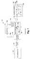
- a conventional PII system 10is shown.
- An RF power plasma source(not shown) is generally inductively or capacitively coupled to a plasma chamber 20 .
- Plasma ignitionis achieved when sufficient power is injected into the system 10 via an RF antenna 30 (shown as an inductor).
- RF antenna 30shown as an inductor.
- poweris injected into the system 10 from a fixed frequency (13.56 MHz) RF generator 40 through a 50 ohm coaxial cable 42 via a matching network 50 .
- the matching network 50is required to provide maximum power to the load by matching the 50 ohm output impedance of the RF generator 40 and a complex impedance established by the power antenna 30 and resultant plasma impedance 60 within the plasma chamber 20 .
- the matching network 50includes mechanically variable high voltage vacuum capacitors 50 a and 50 b .
- the tunable capacitors 50 a and 50 baccount for variations in the antenna impedance caused by changes in plasma impedance 60 before, during and after plasma ignition. Capacitors 50 a and 50 b are employed to minimize “reflected power” back to the RF generator 40 .
- the reflected poweris monitored by a power meter 70 , and a reflected power measurement is provided as an input 70 a to an RF control 72 .
- the controller 72Based on the reflected power input 70 a , the controller 72 directs a control output 72 a to one or more motor drives 74 for adjusting the tunable capacitors 50 a and 50 b in order to minimize reflected power from the load. It is noted, that if the reflected power becomes too high, the RF generator 40 may fault.
- An external inductance 76is depicted between the matching network 50 and the plasma chamber 20 and represents stray inductances associated with the system 10
- the antenna 30 impedancevaries significantly during the plasma ignition phase versus the steady state phase due to the changes caused by the plasma impedance 60 .
- the plasma impedance 60may be roughly modeled as a parallel network containing an imaginary component (X) 60 a and a real component (R) 60 b .
- Ximaginary component
- Rreal component
- large adjustments of the tuning capacitors 50 a and 50 bare generally required to account for large values of reflected power due to changes in plasma impedance 60 during ignition.
- tunabilityis achieved by capacitors 50 a and 50 b
- the delivered poweris often limited to a fraction of the RF generator 40 output capability, and in many cases, plasma ignition is achieved only by increasing the pressure in the plasma source or chamber.
- the process of increasing and subsequently reducing pressure, in conjunction with varying the tuning capacitors 50 a and 50 bmay require more than 10 seconds to complete. This lengthy period of time may enable substantially large voltages to be induced on the antenna 30 and may result in substantial electric fields at the wafer—possibly endangering the devices on the wafer. It is noted that until the plasma is ignited wafers are exposed to the unshielded antenna fields. Furthermore, even before pulsing of the wafer, deposition may occur producing a surface concentration of dopant. Thus, variability in ignition times, source pressures, and voltage transients may result in variations in resultant implant characteristics—making tightly controlled repeatability exceedingly difficult to achieve.
- control system 72and/or any of the related circuits 50 , 70 and/or 74 fail, the plasma will be lost. Even if the control system 72 performs flawlessly, the system 20 is slow to react and move due to the tuning requirements discussed above.
- the present inventionis directed to an integrated power oscillator in a Plasma Immersion Ion Implantation System (PIII) which incorporates a plasma source antenna in the tank circuit of the power oscillator—resulting in generally automatic or immediate passive tracking of the antenna circuit resonant frequency.
- PIIIPlasma Immersion Ion Implantation System
- Thisenables virtually instant ignition of the plasma at pressures to about 0.5 mTorr.
- conventional system componentssuch as controls, tuning capacitors, coupling cables and power feedback meters are eliminated.
- substantially higher repeatability and performanceis achieved over conventional systems.
- the oscillatoris integrated with the plasma source housing and requires only a DC power supply (no RF generator), the present invention substantially reduces the complexity and parts count of the power system and thus provides lower cost and greater reliability over conventional systems.
- the present inventionutilizes characteristics of the plasma source antenna (e.g., antenna inductance) and associated system parameters (e.g., plasma impedance, external system inductance) and incorporates these factors within a power oscillator tank circuit. Since plasma ignition causes significant parametric changes (e.g., plasma impedance changes affecting antenna impedance), the tank circuit and associated power supply are designed to operate across the variable parametric conditions within the plasma chamber. By incorporating the oscillator with the plasma source housing, load reflection and matching problems associated with conventional systems are substantially eliminated.
- the plasma source antennae.g., antenna inductance
- system parameterse.g., plasma impedance, external system inductance
- FIG. 1is a schematic block diagram illustrating a prior art plasma ignition system and associated components in a PIII system
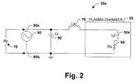
- FIG. 2is a schematic block diagram illustrating an integrated power oscillator system in accordance with the present invention
- FIG. 3is a schematic diagram illustrating an integrated power oscillator system in accordance with an exemplary aspect of the present invention.
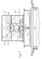
- FIG. 4is a system diagram illustrating a structural relationship between the integrated oscillator system and plasma source chamber in accordance with an exemplary aspect of the present invention.
- the present inventionsubstantially mitigates plasma ignition and operation problems associated with conventional RF plasma power systems.
- Conventional control systems, matching networks, power meters, drives, cables and multiple RF amplifier stagesare eliminated by incorporating existing PIII system parameters such as antenna and plasma impedance within an oscillator circuit designed to accommodate such parameters.
- existing PIII system parameterssuch as antenna and plasma impedance within an oscillator circuit designed to accommodate such parameters.
- FIG. 2a schematic block diagram illustrates an integrated power oscillator system 10 a for providing plasma ignition in a Plasma Immersion Ion Implantation (PIII) system in accordance with the present invention.
- the system 10 ais associated with a PIII system (not shown) for handling, processing and implanting dopants in semiconductor wafers (not shown). Since the wafer handling and processing are well understood in relation to PIII systems, further discussion related thereto is omitted for the purposes of brevity.
- the present inventionmay also be employed to provide etching, ashing, and/or other semiconductor processes such as plasma processing of substrates.
- the present inventionmay also be employed with ultra low energy (ULE) and/or high energy (HE) ion implanters.
- UEEultra low energy
- HEhigh energy
- an integrated power oscillatoris represented by its output resonant tank, including Cr 90, Le 76, La′ 30a and Rs 94, and all other circuitry 80 .
- the active power device(s)which may be solid state or vacuum tube, output to input feedback circuitry, DC power supplies and other support circuitry.
- the plasma chamber 20includes an antenna 30a which can be modeled as an inductance La′, which includes plasma reactive effects.
- a series resistance model Rs 94represents the output tank circuit dissipation, including the resistive part of the plasma load. Any added inductance external to the antenna is represented by Le 76.
- the output tank circuit capacitance 90may include a plurality of capacitors and is selected to set the oscillation frequency to approximately 13.56 MHz. It is to be appreciated that a plurality of other suitable frequencies may also be selected and such variations are contemplated as falling within the scope of the present invention.
- a resonant resistance Rp 78may be determined by analyzing the impedance as seen at nodes 80 a and 80 b . This resistance may be determined as:
- the effective resonant resistance Rp 78depends on antenna design, neutral gas species and pressure, and plasma conditions, and may be adjusted by choice of external inductance Le. Given values for La′ and Le, the approximate operating frequency, f, is chosen by setting the value of Cr 90 as:
- system 10 ais substantially non-linear due the dependence of Rs 94 on plasma density. However, it is sufficient to select system 10 a design parameters based upon the highest value of Rs 94 which generally correlates to the highest plasma density.
- the value of Rs 94is dependant on antenna 30 design, implant species, gas pressure and plasma density and is generally in the range of about 0.5 to 2 ohms.
- the unloaded (no plasma) value of Rs 94is approximately 0.1 ohms.
- the oscillator 80is designed to operate over the ranges of Rs 94 without adjustment so that resistive load changes are accommodated merely by DC power supply current (not shown in FIG. 2 ).
- the resistive load changes caused by changes in plasma densityoccur automatically on a time scale of less than about 1 millisecond.
- plasma reactive effectsmay decrease the value of La′ 30a by about 20% from no load conditions to maximum power, which causes the tank resonant frequency to increase by at most about 10%.
- the oscillator 80is designed according to one exemplary aspect of the present invention to operate within the frequency range caused by the plasma reactive effects without adjustment.
- FIG. 3a schematic diagram depicts an exemplary oscillator circuit 10 b for providing plasma ignition and production in accordance with the present invention.
- Reference numeral 80highlights an oscillator circuit including a vacuum tube 100 , power supplies 100 a and 100 b , a bias network 80 a and various filters which are described in more detail below.
- Reference numeral 90depicts the oscillator output tank circuit capacitance and is represented by a bank of capacitors 101 - 110 . The resonator capacitance 90 is selected to provide sustained oscillation with the oscillator 80 , an external inductance Le 76, a plasma excitation antenna 30 and the plasma (not shown).
- Oscillation of the system 10 bis achieved by providing positive feedback from the output circuit 90 a to the grid element 100 c of the tube 100 .
- Positive feedback to the grid element 100 cprovides a modulation of the tube 100 output current and thereby sustains oscillation. It is to be appreciated that a similar result may be achieved by providing positive feedback to a semiconductor device such as to the gate of a MOSFET and/or other transistor for example.
- DC bias of the grid 100 cis obtained by passing the grid current to ground through a low pass filter, consisting of L 125 (e.g., quarter wave choke, 2 kV, 0.2 A) and C 116 (e.g., 1000 pF, 7.5 kVdc) and resister R 117 (e.g., 2 kohm, 200 W).
- L 125e.g., quarter wave choke, 2 kV, 0.2 A
- C 116e.g., 1000 pF, 7.5 kVdc
- resister R 117e.g., 2 kohm, 200 W.
- the vacuum tube 100is employed to provided the oscillator circuit 10 b output.
- the vacuum tube 100such as an air-cooled Eimac YC245 style, is selected to provide for a robust implementation of the present invention.
- the YC245provides an output power rating of about 4 kW and maximum plate dissipation of about 1.5 kW. It is to be appreciated that other tubes may be chosen. It is further to be appreciated that solid state designs may be selected to implement the present invention such as a power MOSFET and/or other power switching designs.
- the oscillator circuit 10 brepresents a Colpitt's style implementation.
- Plate-to grid positive feedbackis developed through capacitor banks C 101 -C 105 (e.g., approximately 25 pF, 15 kVdc) and C 106 -C 110 (e.g., approximately 200 pF, 15 kVdc), respectively.
- Capacitors 111 and 112e.g., approximately 750 pF, 15 kVdc
- the capacitors in circuit 10 bare selected as standard, low-cost, fixed-value RF transmitting capacitors, however, any type of capacitance may be utilized and is contemplated as falling within the scope of the present invention.
- values for external inductance Le 76 and antenna inductance 30are, for example, approximately (0.2-0.6 uH) and (0.4-0.8 uH), respectively.
- a power supply 100 aprovides heater power for the vacuum tube 100 filament and receives a 120 VAC input (not shown).
- the supply 100 ais selected to be, for example, approximately 6.3 Vdc at about 25 A output capability.
- An RF bypass capacitor 115is selected, for example, as approximately 1000 pF, 7.5 kVdc.
- An oscillator power supply 100 bprovides plate power for the vacuum tube 100 and receives a 208 VAC, three-phase input (not shown).
- the supply 100 bis selected, for example, to be approximately 5 kVdc at about 0.8 A output capability.
- a low pass filter including capacitors 113 , 114 (e.g., approximately 750 pF, 15 kVdc) and inductors 123 , 124couples the supply 100 b output to the tube 100 plate.
- Inductor 123is selected, for example, as a quarter wave choke, 1 kV pk and 1 A, and inductor 124 is selected, for example, as approximately 3 uH.
- FIG. 4a fragmentary structural diagram depicts an integrated power oscillator 10 c and plasma chamber 20 in accordance with one aspect of the present invention.
- the vacuum tube 100is shown operatively coupled to the antenna 30 .
- the antenna 30then couples energy via a quartz plate 138 to the plasma chamber 20 (a bottom portion which contains the wafer to be processed is not shown).
- a fan 140provides cooling for the tube 100 .
- the present inventionprovides substantial improvements over prior art systems—notably, repeatable plasma ignition, lower cost, higher reliability and faster ignition times.
- the inventionincludes a computer-readable medium having computer-executable instructions for performing the steps of the various methods of the invention.
- a particular feature of the inventionmay have been disclosed with respect to only one of several embodiments, such feature may be combined with one or more other features of the other embodiments as may be desired and advantageous for any given or particular application.
- the terms “includes”, “including”, “has”, “having”, and variants thereofare used in either the detailed description or the claims, these terms are intended to be inclusive in a manner similar to the term “comprising”.
Landscapes
- Physics & Mathematics (AREA)
- Engineering & Computer Science (AREA)
- Plasma & Fusion (AREA)
- Chemical & Material Sciences (AREA)
- Analytical Chemistry (AREA)
- Spectroscopy & Molecular Physics (AREA)
- Plasma Technology (AREA)
- Physical Vapour Deposition (AREA)
- Physical Or Chemical Processes And Apparatus (AREA)
- Drying Of Semiconductors (AREA)
- Electron Sources, Ion Sources (AREA)
Abstract
Description
Claims (19)
Priority Applications (6)
| Application Number | Priority Date | Filing Date | Title |
|---|---|---|---|
| US09/619,839US6305316B1 (en) | 2000-07-20 | 2000-07-20 | Integrated power oscillator RF source of plasma immersion ion implantation system |
| TW090116550ATW494711B (en) | 2000-07-20 | 2001-07-06 | Integrated power oscillator RF source for plasma immersion ion implantation system |
| EP01306072AEP1174901A3 (en) | 2000-07-20 | 2001-07-13 | Integrated power oscillator RF source for plasma immersion ion implantation system |
| KR1020010043078AKR20020011075A (en) | 2000-07-20 | 2001-07-18 | Integrated power oscillator rf source for plasma immersion ion implantation system |
| JP2001219685AJP2002151429A (en) | 2000-07-20 | 2001-07-19 | Rf plasma generator and wafer processing system |
| SG200104422ASG108263A1 (en) | 2000-07-20 | 2001-07-20 | Integrated power oscillator rf source for plasma immersion ion implantation system |
Applications Claiming Priority (1)
| Application Number | Priority Date | Filing Date | Title |
|---|---|---|---|
| US09/619,839US6305316B1 (en) | 2000-07-20 | 2000-07-20 | Integrated power oscillator RF source of plasma immersion ion implantation system |
Publications (1)
| Publication Number | Publication Date |
|---|---|
| US6305316B1true US6305316B1 (en) | 2001-10-23 |
Family
ID=24483518
Family Applications (1)
| Application Number | Title | Priority Date | Filing Date |
|---|---|---|---|
| US09/619,839Expired - Fee RelatedUS6305316B1 (en) | 2000-07-20 | 2000-07-20 | Integrated power oscillator RF source of plasma immersion ion implantation system |
Country Status (6)
| Country | Link |
|---|---|
| US (1) | US6305316B1 (en) |
| EP (1) | EP1174901A3 (en) |
| JP (1) | JP2002151429A (en) |
| KR (1) | KR20020011075A (en) |
| SG (1) | SG108263A1 (en) |
| TW (1) | TW494711B (en) |
Cited By (47)
| Publication number | Priority date | Publication date | Assignee | Title |
|---|---|---|---|---|
| US6452196B1 (en)* | 1999-12-20 | 2002-09-17 | Axcelis Technologies, Inc. | Power supply hardening for ion beam systems |
| US6531031B1 (en)* | 1999-01-07 | 2003-03-11 | Robert Bosch Gmbh | Plasma etching installation |
| US20030150710A1 (en)* | 2001-10-09 | 2003-08-14 | Evans John D. | Plasma production device and method and RF driver circuit |
| US20030226641A1 (en)* | 2000-08-11 | 2003-12-11 | Applied Materials, Inc. | Externally excited torroidal plasma source with magnetic control of ion distribution |
| US20040026231A1 (en)* | 2001-10-09 | 2004-02-12 | Pribyl Patrick A. | Plasma production device and method and RF driver circuit with adjustable duty cycle |
| US20040263412A1 (en)* | 2001-10-09 | 2004-12-30 | Patrick Pribyl | Plasma production device and method and RF driver circuit with adjustable duty cycle |
| US20050098117A1 (en)* | 2003-11-06 | 2005-05-12 | Divergilio William F. | Segmented resonant antenna for radio frequency inductively coupled plasmas |
| US20050098742A1 (en)* | 2003-11-06 | 2005-05-12 | Kellerman Peter L. | System and method for performing SIMOX implants using an ion shower |
| US6893907B2 (en) | 2002-06-05 | 2005-05-17 | Applied Materials, Inc. | Fabrication of silicon-on-insulator structure using plasma immersion ion implantation |
| US20050127844A1 (en)* | 2002-03-14 | 2005-06-16 | Mitsubishi Heavy Industries, Ltd | High-frequency power supply structure and plasma cvd device using the same |
| US20050134186A1 (en)* | 2003-12-19 | 2005-06-23 | Brouk Victor L. | Stabilizing plasma and generator interactions |
| US7037813B2 (en) | 2000-08-11 | 2006-05-02 | Applied Materials, Inc. | Plasma immersion ion implantation process using a capacitively coupled plasma source having low dissociation and low minimum plasma voltage |
| US7094316B1 (en) | 2000-08-11 | 2006-08-22 | Applied Materials, Inc. | Externally excited torroidal plasma source |
| US7094670B2 (en) | 2000-08-11 | 2006-08-22 | Applied Materials, Inc. | Plasma immersion ion implantation process |
| US7109098B1 (en) | 2005-05-17 | 2006-09-19 | Applied Materials, Inc. | Semiconductor junction formation process including low temperature plasma deposition of an optical absorption layer and high speed optical annealing |
| US7137354B2 (en) | 2000-08-11 | 2006-11-21 | Applied Materials, Inc. | Plasma immersion ion implantation apparatus including a plasma source having low dissociation and low minimum plasma voltage |
| US7166524B2 (en) | 2000-08-11 | 2007-01-23 | Applied Materials, Inc. | Method for ion implanting insulator material to reduce dielectric constant |
| US7183177B2 (en) | 2000-08-11 | 2007-02-27 | Applied Materials, Inc. | Silicon-on-insulator wafer transfer method using surface activation plasma immersion ion implantation for wafer-to-wafer adhesion enhancement |
| US7223676B2 (en) | 2002-06-05 | 2007-05-29 | Applied Materials, Inc. | Very low temperature CVD process with independently variable conformality, stress and composition of the CVD layer |
| US7244474B2 (en) | 2004-03-26 | 2007-07-17 | Applied Materials, Inc. | Chemical vapor deposition plasma process using an ion shower grid |
| US7288491B2 (en) | 2000-08-11 | 2007-10-30 | Applied Materials, Inc. | Plasma immersion ion implantation process |
| US7291360B2 (en) | 2004-03-26 | 2007-11-06 | Applied Materials, Inc. | Chemical vapor deposition plasma process using plural ion shower grids |
| US7294563B2 (en) | 2000-08-10 | 2007-11-13 | Applied Materials, Inc. | Semiconductor on insulator vertical transistor fabrication and doping process |
| US7303982B2 (en) | 2000-08-11 | 2007-12-04 | Applied Materials, Inc. | Plasma immersion ion implantation process using an inductively coupled plasma source having low dissociation and low minimum plasma voltage |
| US7312162B2 (en) | 2005-05-17 | 2007-12-25 | Applied Materials, Inc. | Low temperature plasma deposition process for carbon layer deposition |
| US7312148B2 (en) | 2005-08-08 | 2007-12-25 | Applied Materials, Inc. | Copper barrier reflow process employing high speed optical annealing |
| US7320734B2 (en) | 2000-08-11 | 2008-01-22 | Applied Materials, Inc. | Plasma immersion ion implantation system including a plasma source having low dissociation and low minimum plasma voltage |
| US7323401B2 (en) | 2005-08-08 | 2008-01-29 | Applied Materials, Inc. | Semiconductor substrate process using a low temperature deposited carbon-containing hard mask |
| US7335611B2 (en) | 2005-08-08 | 2008-02-26 | Applied Materials, Inc. | Copper conductor annealing process employing high speed optical annealing with a low temperature-deposited optical absorber layer |
| EP1689907A4 (en)* | 2003-06-19 | 2008-07-23 | Plasma Control Systems Llc | Plasma production device and method and rf driver circuit with adjustable duty cycle |
| US7422775B2 (en) | 2005-05-17 | 2008-09-09 | Applied Materials, Inc. | Process for low temperature plasma deposition of an optical absorption layer and high speed optical annealing |
| US7429532B2 (en) | 2005-08-08 | 2008-09-30 | Applied Materials, Inc. | Semiconductor substrate process using an optically writable carbon-containing mask |
| US7428915B2 (en) | 2005-04-26 | 2008-09-30 | Applied Materials, Inc. | O-ringless tandem throttle valve for a plasma reactor chamber |
| US7430984B2 (en) | 2000-08-11 | 2008-10-07 | Applied Materials, Inc. | Method to drive spatially separate resonant structure with spatially distinct plasma secondaries using a single generator and switching elements |
| US7465478B2 (en) | 2000-08-11 | 2008-12-16 | Applied Materials, Inc. | Plasma immersion ion implantation process |
| US7479456B2 (en) | 2004-08-26 | 2009-01-20 | Applied Materials, Inc. | Gasless high voltage high contact force wafer contact-cooling electrostatic chuck |
| US7666464B2 (en) | 2004-10-23 | 2010-02-23 | Applied Materials, Inc. | RF measurement feedback control and diagnostics for a plasma immersion ion implantation reactor |
| US20100072401A1 (en)* | 2008-09-25 | 2010-03-25 | Twin Creeks Technologies, Inc. | Hydrogen ion implanter using a broad beam source |
| US7695590B2 (en) | 2004-03-26 | 2010-04-13 | Applied Materials, Inc. | Chemical vapor deposition plasma reactor having plural ion shower grids |
| US7767561B2 (en) | 2004-07-20 | 2010-08-03 | Applied Materials, Inc. | Plasma immersion ion implantation reactor having an ion shower grid |
| US20100270141A1 (en)* | 2009-04-27 | 2010-10-28 | Advanced Energy Industries, Inc. | Detecting and Preventing Instabilities in Plasma Processes |
| US8058156B2 (en) | 2004-07-20 | 2011-11-15 | Applied Materials, Inc. | Plasma immersion ion implantation reactor having multiple ion shower grids |
| US20120279657A1 (en)* | 2011-05-06 | 2012-11-08 | Axcelis Technologies, Inc. | RF Coupled Plasma Abatement System Comprising an Integrated Power Oscillator |
| US20140272182A1 (en)* | 2013-03-14 | 2014-09-18 | Varian Semiconductor Equipment Associates, Inc. | Method For Implementing Low Dose Implant In A Plasma System |
| GB2479702B (en)* | 2009-02-27 | 2015-06-03 | Mks Instr Inc | Method and apparatus of providing power to ignite and sustain a plasma in a reactive gas generator |
| US11195697B2 (en)* | 2016-01-22 | 2021-12-07 | Spp Technologies Co., Ltd. | Plasma control apparatus |
| US20220084791A1 (en)* | 2014-01-10 | 2022-03-17 | Reno Technologies, Inc. | Rf impedance matching network |
Families Citing this family (11)
| Publication number | Priority date | Publication date | Assignee | Title |
|---|---|---|---|---|
| US7459899B2 (en) | 2005-11-21 | 2008-12-02 | Thermo Fisher Scientific Inc. | Inductively-coupled RF power source |
| WO2009146439A1 (en) | 2008-05-30 | 2009-12-03 | Colorado State University Research Foundation | System, method and apparatus for generating plasma |
| US9288886B2 (en) | 2008-05-30 | 2016-03-15 | Colorado State University Research Foundation | Plasma-based chemical source device and method of use thereof |
| US8994270B2 (en) | 2008-05-30 | 2015-03-31 | Colorado State University Research Foundation | System and methods for plasma application |
| US8222822B2 (en) | 2009-10-27 | 2012-07-17 | Tyco Healthcare Group Lp | Inductively-coupled plasma device |
| CA2794895A1 (en) | 2010-03-31 | 2011-10-06 | Colorado State University Research Foundation | Liquid-gas interface plasma device |
| EP2552340A4 (en) | 2010-03-31 | 2015-10-14 | Univ Colorado State Res Found | PLASMA DEVICE WITH LIQUID-GAS INTERFACE |
| CN102740580B (en)* | 2012-06-27 | 2015-08-19 | 华东师范大学 | A kind of Small-power microwave microplasma integration source |
| JP2014049362A (en)* | 2012-09-03 | 2014-03-17 | Tokyo Electron Ltd | Plasma generation device and substrate processing device |
| US9532826B2 (en) | 2013-03-06 | 2017-01-03 | Covidien Lp | System and method for sinus surgery |
| US9555145B2 (en) | 2013-03-13 | 2017-01-31 | Covidien Lp | System and method for biofilm remediation |
Citations (9)
| Publication number | Priority date | Publication date | Assignee | Title |
|---|---|---|---|---|
| US3832648A (en)* | 1973-05-29 | 1974-08-27 | Dowell R Mc | Radio frequency power generator utilizing non-magnetic slug tuned coils and impedance matching network for use therewith |
| US3958883A (en)* | 1974-07-10 | 1976-05-25 | Baird-Atomic, Inc. | Radio frequency induced plasma excitation of optical emission spectroscopic samples |
| US4667111A (en) | 1985-05-17 | 1987-05-19 | Eaton Corporation | Accelerator for ion implantation |
| US5212425A (en)* | 1990-10-10 | 1993-05-18 | Hughes Aircraft Company | Ion implantation and surface processing method and apparatus |
| US5643364A (en)* | 1994-11-30 | 1997-07-01 | Applied Materials, Inc. | Plasma chamber with fixed RF matching |
| US5654043A (en) | 1996-10-10 | 1997-08-05 | Eaton Corporation | Pulsed plate plasma implantation system and method |
| US5911832A (en)* | 1996-10-10 | 1999-06-15 | Eaton Corporation | Plasma immersion implantation with pulsed anode |
| US5942855A (en)* | 1996-08-28 | 1999-08-24 | Northeastern University | Monolithic miniaturized inductively coupled plasma source |
| US6027601A (en) | 1997-07-01 | 2000-02-22 | Applied Materials, Inc | Automatic frequency tuning of an RF plasma source of an inductively coupled plasma reactor |
Family Cites Families (9)
| Publication number | Priority date | Publication date | Assignee | Title |
|---|---|---|---|---|
| FR2460589A1 (en)* | 1979-07-04 | 1981-01-23 | Instruments Sa | PLASMA GENERATOR |
| GB8905073D0 (en)* | 1989-03-06 | 1989-04-19 | Nordiko Ltd | Ion gun |
| JP3167221B2 (en)* | 1992-05-07 | 2001-05-21 | ザ・パーキン・エルマー・コーポレイション | Inductively coupled plasma generator |
| GB9714341D0 (en)* | 1997-07-09 | 1997-09-10 | Surface Tech Sys Ltd | Plasma processing apparatus |
| US6168690B1 (en)* | 1997-09-29 | 2001-01-02 | Lam Research Corporation | Methods and apparatus for physical vapor deposition |
| JPH11145148A (en)* | 1997-11-06 | 1999-05-28 | Tdk Corp | Apparatus and method for heat plasma annealing |
| JP3840821B2 (en)* | 1998-11-30 | 2006-11-01 | 株式会社日立製作所 | Plasma processing equipment |
| JP2002531914A (en)* | 1998-12-01 | 2002-09-24 | シリコン ジェネシス コーポレイション | Enhanced plasma mode, method and system for plasma immersion ion implantation |
| JP4672941B2 (en)* | 1999-07-13 | 2011-04-20 | 東京エレクトロン株式会社 | High frequency power supply for generating inductively coupled plasma |
- 2000
- 2000-07-20USUS09/619,839patent/US6305316B1/ennot_activeExpired - Fee Related
- 2001
- 2001-07-06TWTW090116550Apatent/TW494711B/ennot_activeIP Right Cessation
- 2001-07-13EPEP01306072Apatent/EP1174901A3/ennot_activeCeased
- 2001-07-18KRKR1020010043078Apatent/KR20020011075A/ennot_activeCeased
- 2001-07-19JPJP2001219685Apatent/JP2002151429A/enactivePending
- 2001-07-20SGSG200104422Apatent/SG108263A1/enunknown
Patent Citations (10)
| Publication number | Priority date | Publication date | Assignee | Title |
|---|---|---|---|---|
| US3832648A (en)* | 1973-05-29 | 1974-08-27 | Dowell R Mc | Radio frequency power generator utilizing non-magnetic slug tuned coils and impedance matching network for use therewith |
| US3958883A (en)* | 1974-07-10 | 1976-05-25 | Baird-Atomic, Inc. | Radio frequency induced plasma excitation of optical emission spectroscopic samples |
| US4667111A (en) | 1985-05-17 | 1987-05-19 | Eaton Corporation | Accelerator for ion implantation |
| US4667111C1 (en) | 1985-05-17 | 2001-04-10 | Eaton Corp Cleveland | Accelerator for ion implantation |
| US5212425A (en)* | 1990-10-10 | 1993-05-18 | Hughes Aircraft Company | Ion implantation and surface processing method and apparatus |
| US5643364A (en)* | 1994-11-30 | 1997-07-01 | Applied Materials, Inc. | Plasma chamber with fixed RF matching |
| US5942855A (en)* | 1996-08-28 | 1999-08-24 | Northeastern University | Monolithic miniaturized inductively coupled plasma source |
| US5654043A (en) | 1996-10-10 | 1997-08-05 | Eaton Corporation | Pulsed plate plasma implantation system and method |
| US5911832A (en)* | 1996-10-10 | 1999-06-15 | Eaton Corporation | Plasma immersion implantation with pulsed anode |
| US6027601A (en) | 1997-07-01 | 2000-02-22 | Applied Materials, Inc | Automatic frequency tuning of an RF plasma source of an inductively coupled plasma reactor |
Cited By (67)
| Publication number | Priority date | Publication date | Assignee | Title |
|---|---|---|---|---|
| US6531031B1 (en)* | 1999-01-07 | 2003-03-11 | Robert Bosch Gmbh | Plasma etching installation |
| US6452196B1 (en)* | 1999-12-20 | 2002-09-17 | Axcelis Technologies, Inc. | Power supply hardening for ion beam systems |
| US7294563B2 (en) | 2000-08-10 | 2007-11-13 | Applied Materials, Inc. | Semiconductor on insulator vertical transistor fabrication and doping process |
| US7288491B2 (en) | 2000-08-11 | 2007-10-30 | Applied Materials, Inc. | Plasma immersion ion implantation process |
| US7183177B2 (en) | 2000-08-11 | 2007-02-27 | Applied Materials, Inc. | Silicon-on-insulator wafer transfer method using surface activation plasma immersion ion implantation for wafer-to-wafer adhesion enhancement |
| US7430984B2 (en) | 2000-08-11 | 2008-10-07 | Applied Materials, Inc. | Method to drive spatially separate resonant structure with spatially distinct plasma secondaries using a single generator and switching elements |
| US7465478B2 (en) | 2000-08-11 | 2008-12-16 | Applied Materials, Inc. | Plasma immersion ion implantation process |
| US20030226641A1 (en)* | 2000-08-11 | 2003-12-11 | Applied Materials, Inc. | Externally excited torroidal plasma source with magnetic control of ion distribution |
| US7137354B2 (en) | 2000-08-11 | 2006-11-21 | Applied Materials, Inc. | Plasma immersion ion implantation apparatus including a plasma source having low dissociation and low minimum plasma voltage |
| US7320734B2 (en) | 2000-08-11 | 2008-01-22 | Applied Materials, Inc. | Plasma immersion ion implantation system including a plasma source having low dissociation and low minimum plasma voltage |
| US7291545B2 (en) | 2000-08-11 | 2007-11-06 | Applied Materials, Inc. | Plasma immersion ion implantation process using a capacitively couple plasma source having low dissociation and low minimum plasma voltage |
| US7166524B2 (en) | 2000-08-11 | 2007-01-23 | Applied Materials, Inc. | Method for ion implanting insulator material to reduce dielectric constant |
| US6939434B2 (en) | 2000-08-11 | 2005-09-06 | Applied Materials, Inc. | Externally excited torroidal plasma source with magnetic control of ion distribution |
| US7037813B2 (en) | 2000-08-11 | 2006-05-02 | Applied Materials, Inc. | Plasma immersion ion implantation process using a capacitively coupled plasma source having low dissociation and low minimum plasma voltage |
| US7303982B2 (en) | 2000-08-11 | 2007-12-04 | Applied Materials, Inc. | Plasma immersion ion implantation process using an inductively coupled plasma source having low dissociation and low minimum plasma voltage |
| US7094316B1 (en) | 2000-08-11 | 2006-08-22 | Applied Materials, Inc. | Externally excited torroidal plasma source |
| US7094670B2 (en) | 2000-08-11 | 2006-08-22 | Applied Materials, Inc. | Plasma immersion ion implantation process |
| US7084832B2 (en)* | 2001-10-09 | 2006-08-01 | Plasma Control Systems, Llc | Plasma production device and method and RF driver circuit with adjustable duty cycle |
| US7132996B2 (en) | 2001-10-09 | 2006-11-07 | Plasma Control Systems Llc | Plasma production device and method and RF driver circuit |
| US7100532B2 (en) | 2001-10-09 | 2006-09-05 | Plasma Control Systems, Llc | Plasma production device and method and RF driver circuit with adjustable duty cycle |
| US20030150710A1 (en)* | 2001-10-09 | 2003-08-14 | Evans John D. | Plasma production device and method and RF driver circuit |
| US20040026231A1 (en)* | 2001-10-09 | 2004-02-12 | Pribyl Patrick A. | Plasma production device and method and RF driver circuit with adjustable duty cycle |
| US20040263412A1 (en)* | 2001-10-09 | 2004-12-30 | Patrick Pribyl | Plasma production device and method and RF driver circuit with adjustable duty cycle |
| US7319295B2 (en)* | 2002-03-14 | 2008-01-15 | Mitsubishi Heavy Industries, Ltd. | High-frequency power supply structure and plasma CVD device using the same |
| US20050127844A1 (en)* | 2002-03-14 | 2005-06-16 | Mitsubishi Heavy Industries, Ltd | High-frequency power supply structure and plasma cvd device using the same |
| US7700465B2 (en) | 2002-06-05 | 2010-04-20 | Applied Materials, Inc. | Plasma immersion ion implantation process using a plasma source having low dissociation and low minimum plasma voltage |
| US7223676B2 (en) | 2002-06-05 | 2007-05-29 | Applied Materials, Inc. | Very low temperature CVD process with independently variable conformality, stress and composition of the CVD layer |
| US6893907B2 (en) | 2002-06-05 | 2005-05-17 | Applied Materials, Inc. | Fabrication of silicon-on-insulator structure using plasma immersion ion implantation |
| US7393765B2 (en) | 2002-06-05 | 2008-07-01 | Applied Materials, Inc. | Low temperature CVD process with selected stress of the CVD layer on CMOS devices |
| EP1620915A4 (en)* | 2003-04-17 | 2008-07-23 | Plasma Control Systems Llc | Plasma production device and method and rf driver circuit with adjustable duty cycle |
| EP1689907A4 (en)* | 2003-06-19 | 2008-07-23 | Plasma Control Systems Llc | Plasma production device and method and rf driver circuit with adjustable duty cycle |
| US7748344B2 (en) | 2003-11-06 | 2010-07-06 | Axcelis Technologies, Inc. | Segmented resonant antenna for radio frequency inductively coupled plasmas |
| US7421973B2 (en) | 2003-11-06 | 2008-09-09 | Axcelis Technologies, Inc. | System and method for performing SIMOX implants using an ion shower |
| US20050098117A1 (en)* | 2003-11-06 | 2005-05-12 | Divergilio William F. | Segmented resonant antenna for radio frequency inductively coupled plasmas |
| US20050098742A1 (en)* | 2003-11-06 | 2005-05-12 | Kellerman Peter L. | System and method for performing SIMOX implants using an ion shower |
| US20070044717A1 (en)* | 2003-11-06 | 2007-03-01 | Divergilio William F | Segmented resonant antenna for radio frequency inductively coupled plasmas |
| US7157857B2 (en)* | 2003-12-19 | 2007-01-02 | Advanced Energy Industries, Inc. | Stabilizing plasma and generator interactions |
| WO2005066991A1 (en)* | 2003-12-19 | 2005-07-21 | Advanced Energy Industries, Inc. | Stabilizing plasma and generator interactions |
| US20050134186A1 (en)* | 2003-12-19 | 2005-06-23 | Brouk Victor L. | Stabilizing plasma and generator interactions |
| US7695590B2 (en) | 2004-03-26 | 2010-04-13 | Applied Materials, Inc. | Chemical vapor deposition plasma reactor having plural ion shower grids |
| US7244474B2 (en) | 2004-03-26 | 2007-07-17 | Applied Materials, Inc. | Chemical vapor deposition plasma process using an ion shower grid |
| US7291360B2 (en) | 2004-03-26 | 2007-11-06 | Applied Materials, Inc. | Chemical vapor deposition plasma process using plural ion shower grids |
| US8058156B2 (en) | 2004-07-20 | 2011-11-15 | Applied Materials, Inc. | Plasma immersion ion implantation reactor having multiple ion shower grids |
| US7767561B2 (en) | 2004-07-20 | 2010-08-03 | Applied Materials, Inc. | Plasma immersion ion implantation reactor having an ion shower grid |
| US7479456B2 (en) | 2004-08-26 | 2009-01-20 | Applied Materials, Inc. | Gasless high voltage high contact force wafer contact-cooling electrostatic chuck |
| US7666464B2 (en) | 2004-10-23 | 2010-02-23 | Applied Materials, Inc. | RF measurement feedback control and diagnostics for a plasma immersion ion implantation reactor |
| US7428915B2 (en) | 2005-04-26 | 2008-09-30 | Applied Materials, Inc. | O-ringless tandem throttle valve for a plasma reactor chamber |
| US7109098B1 (en) | 2005-05-17 | 2006-09-19 | Applied Materials, Inc. | Semiconductor junction formation process including low temperature plasma deposition of an optical absorption layer and high speed optical annealing |
| US7422775B2 (en) | 2005-05-17 | 2008-09-09 | Applied Materials, Inc. | Process for low temperature plasma deposition of an optical absorption layer and high speed optical annealing |
| US7312162B2 (en) | 2005-05-17 | 2007-12-25 | Applied Materials, Inc. | Low temperature plasma deposition process for carbon layer deposition |
| US7323401B2 (en) | 2005-08-08 | 2008-01-29 | Applied Materials, Inc. | Semiconductor substrate process using a low temperature deposited carbon-containing hard mask |
| US7335611B2 (en) | 2005-08-08 | 2008-02-26 | Applied Materials, Inc. | Copper conductor annealing process employing high speed optical annealing with a low temperature-deposited optical absorber layer |
| US7312148B2 (en) | 2005-08-08 | 2007-12-25 | Applied Materials, Inc. | Copper barrier reflow process employing high speed optical annealing |
| US7429532B2 (en) | 2005-08-08 | 2008-09-30 | Applied Materials, Inc. | Semiconductor substrate process using an optically writable carbon-containing mask |
| US20100072401A1 (en)* | 2008-09-25 | 2010-03-25 | Twin Creeks Technologies, Inc. | Hydrogen ion implanter using a broad beam source |
| US7897945B2 (en) | 2008-09-25 | 2011-03-01 | Twin Creeks Technologies, Inc. | Hydrogen ion implanter using a broad beam source |
| GB2479702B (en)* | 2009-02-27 | 2015-06-03 | Mks Instr Inc | Method and apparatus of providing power to ignite and sustain a plasma in a reactive gas generator |
| US8674606B2 (en) | 2009-04-27 | 2014-03-18 | Advanced Energy Industries, Inc. | Detecting and preventing instabilities in plasma processes |
| US20100270141A1 (en)* | 2009-04-27 | 2010-10-28 | Advanced Energy Industries, Inc. | Detecting and Preventing Instabilities in Plasma Processes |
| WO2012154217A1 (en)* | 2011-05-06 | 2012-11-15 | Axcelis Technologies, Inc. | Rf coupled plasma abatement system comprising an integrated power oscillator |
| US20120279657A1 (en)* | 2011-05-06 | 2012-11-08 | Axcelis Technologies, Inc. | RF Coupled Plasma Abatement System Comprising an Integrated Power Oscillator |
| US8932430B2 (en)* | 2011-05-06 | 2015-01-13 | Axcelis Technologies, Inc. | RF coupled plasma abatement system comprising an integrated power oscillator |
| US20140272182A1 (en)* | 2013-03-14 | 2014-09-18 | Varian Semiconductor Equipment Associates, Inc. | Method For Implementing Low Dose Implant In A Plasma System |
| US9783884B2 (en)* | 2013-03-14 | 2017-10-10 | Varian Semiconductor Equipment Associates, Inc. | Method for implementing low dose implant in a plasma system |
| US20220084791A1 (en)* | 2014-01-10 | 2022-03-17 | Reno Technologies, Inc. | Rf impedance matching network |
| US12334306B2 (en)* | 2014-01-10 | 2025-06-17 | Asm America, Inc. | RF impedance matching network |
| US11195697B2 (en)* | 2016-01-22 | 2021-12-07 | Spp Technologies Co., Ltd. | Plasma control apparatus |
Also Published As
| Publication number | Publication date |
|---|---|
| EP1174901A2 (en) | 2002-01-23 |
| EP1174901A3 (en) | 2004-09-15 |
| TW494711B (en) | 2002-07-11 |
| JP2002151429A (en) | 2002-05-24 |
| KR20020011075A (en) | 2002-02-07 |
| SG108263A1 (en) | 2005-01-28 |
Similar Documents
| Publication | Publication Date | Title |
|---|---|---|
| US6305316B1 (en) | Integrated power oscillator RF source of plasma immersion ion implantation system | |
| US10450653B2 (en) | High impedance RF filter for heater with impedance tuning device | |
| US6030667A (en) | Apparatus and method for applying RF power apparatus and method for generating plasma and apparatus and method for processing with plasma | |
| EP0412568B1 (en) | Matching network and method for using same | |
| US5849136A (en) | High frequency semiconductor wafer processing apparatus and method | |
| TWI355015B (en) | Dual frequency rf match | |
| US6740842B2 (en) | Radio frequency power source for generating an inductively coupled plasma | |
| US5223457A (en) | High-frequency semiconductor wafer processing method using a negative self-bias | |
| EP0840350A2 (en) | Plasma apparatus and process with filtering of plasma sheath-generated harmonics | |
| US7480571B2 (en) | Apparatus and methods for improving the stability of RF power delivery to a plasma load | |
| US6677711B2 (en) | Plasma processor method and apparatus | |
| US5585766A (en) | Electrically tuned matching networks using adjustable inductance elements | |
| JPH10241894A (en) | High frequency tuning method for high frequency plasma reactor using frequency servo and control of power, voltage, current or dI / dt | |
| US6537421B2 (en) | RF bias control in plasma deposition and etch systems with multiple RF power sources | |
| EP0421430B1 (en) | A plasma process, method and apparatus | |
| KR20240043808A (en) | Distortion Current Mitigation in Radio Frequency Plasma Processing Chambers | |
| WO2022078336A1 (en) | Impedance matching method, impedance matcher and semiconductor process device | |
| KR100648336B1 (en) | Apparatus and methods for a fixed impedance transformation network for use in connection with a plasma chamber | |
| US6954033B2 (en) | Plasma processing apparatus | |
| US6838832B1 (en) | Apparatus and methods for improving the stability of RF power delivery to a plasma load | |
| CN113604788A (en) | Base bias adjusting device and method and semiconductor process equipment | |
| CN116759284A (en) | Semiconductor process equipment, optimal impedance value acquisition method and sweep frequency matching method | |
| CN113066712B (en) | Impedance matching method and semiconductor process equipment | |
| US20250218748A1 (en) | Air-core coil in analog circuit filters for plasma processing | |
| US20240371605A1 (en) | Fast tuning radio frequency (rf) matching network |
Legal Events
| Date | Code | Title | Description |
|---|---|---|---|
| AS | Assignment | Owner name:AXCELIS TECHNOLOGIES, INC., MASSACHUSETTS Free format text:ASSIGNMENT OF ASSIGNORS INTEREST;ASSIGNORS:DIVERGILIO, WILLIAM F.;KELLERMAN, PETER L.;RYAN, KEVIN T.;REEL/FRAME:010963/0034 Effective date:20000714 | |
| CC | Certificate of correction | ||
| FPAY | Fee payment | Year of fee payment:4 | |
| AS | Assignment | Owner name:SILICON VALLEY BANK, CALIFORNIA Free format text:SECURITY AGREEMENT;ASSIGNOR:AXCELIS TECHNOLOGIES, INC.;REEL/FRAME:020986/0143 Effective date:20080423 Owner name:SILICON VALLEY BANK,CALIFORNIA Free format text:SECURITY AGREEMENT;ASSIGNOR:AXCELIS TECHNOLOGIES, INC.;REEL/FRAME:020986/0143 Effective date:20080423 | |
| AS | Assignment | Owner name:SEN CORPORATION, JAPAN Free format text:CONSENT AND LICENSE AGREEMENT;ASSIGNOR:AXCELIS TECHNOLOGIES, INC.;REEL/FRAME:022562/0758 Effective date:20090330 Owner name:SEN CORPORATION,JAPAN Free format text:CONSENT AND LICENSE AGREEMENT;ASSIGNOR:AXCELIS TECHNOLOGIES, INC.;REEL/FRAME:022562/0758 Effective date:20090330 | |
| REMI | Maintenance fee reminder mailed | ||
| LAPS | Lapse for failure to pay maintenance fees | ||
| STCH | Information on status: patent discontinuation | Free format text:PATENT EXPIRED DUE TO NONPAYMENT OF MAINTENANCE FEES UNDER 37 CFR 1.362 | |
| FP | Lapsed due to failure to pay maintenance fee | Effective date:20091023 |