US6304945B1 - Method and apparatus for maintaining cache coherency in a computer system having multiple processor buses - Google Patents
Method and apparatus for maintaining cache coherency in a computer system having multiple processor busesDownload PDFInfo
- Publication number
- US6304945B1 US6304945B1US09/311,082US31108299AUS6304945B1US 6304945 B1US6304945 B1US 6304945B1US 31108299 AUS31108299 AUS 31108299AUS 6304945 B1US6304945 B1US 6304945B1
- Authority
- US
- United States
- Prior art keywords
- memory
- address
- request
- coherency
- information
- Prior art date
- Legal status (The legal status is an assumption and is not a legal conclusion. Google has not performed a legal analysis and makes no representation as to the accuracy of the status listed.)
- Expired - Lifetime
Links
Images

Classifications
- G—PHYSICS
- G06—COMPUTING OR CALCULATING; COUNTING
- G06F—ELECTRIC DIGITAL DATA PROCESSING
- G06F12/00—Accessing, addressing or allocating within memory systems or architectures
- G06F12/02—Addressing or allocation; Relocation
- G06F12/08—Addressing or allocation; Relocation in hierarchically structured memory systems, e.g. virtual memory systems
- G06F12/0802—Addressing of a memory level in which the access to the desired data or data block requires associative addressing means, e.g. caches
- G06F12/0806—Multiuser, multiprocessor or multiprocessing cache systems
- G06F12/0815—Cache consistency protocols
- G06F12/0817—Cache consistency protocols using directory methods
- G06F12/082—Associative directories
Definitions
- This inventionrelates generally to computer systems having multiple processors with cache memories, and, more particularly, to a method and apparatus for maintaining cache coherency in a computer system having multiple processor buses.
- the speed of a computer systemis determined by its processing bandwidth, and the amount of data it may readily retrieve.
- the processing poweris determined, in part, by the number of processors in the computer system and the speed of those processors.
- datais read from a fixed storage device (e.g., hard disk) and stored in a main memory device in the computer system for later retrieval by the processor(s).
- Many transactions in the computer systemare directed toward reading or writing to the main memory.
- the memory controllersare coupled to a single, shared memory bus.
- processorsIn many computer systems, multiple processors are used to increase system performance.
- processorstypically have a cache memory.
- a cache memorymaintains a local copy of selected lines of data contained in the main memory for rapid retrieval.
- Cache memoriesare typically implemented using fast, static random access memories (SRAM), and main memories are typically implemented in higher-density, but slower, dynamic random access memories (DRAM). Because two or more processors may be involved with executing a single software application, the same memory lines may be stored in the cache memories of different processors.
- SRAMstatic random access memories
- DRAMdynamic random access memories
- Past computer systemshave included multiple processors and multiple memory controllers coupled to the same shared bus. As the frequency of the bus increases, the number of electrical loads supportable on the bus decreases. To maintain or increase the number of processors while increasing the bus speed, the processors are split across multiple processor buses. Due to the segregation of processors onto separate processor buses, it is necessary to maintain the coherency of the processor cache memories across the buses.
- Cache line statesmay be invalid, shared, or owned. Invalid states indicate that the line is not cached anywhere in the system.
- the shared stateindicates that the line may be present in one or more processor caches.
- the owned stateindicates that the line may be in an exclusive or modified state in one of the caches.
- One technique for maintaining cache coherencyinvolves the use of a cache directory associated with each of the memory controllers. Each memory controller accesses mutually exclusive address ranges.
- the cache directorystores the status of each of the cacheable memory lines governed by the associated memory controller. Due to the large number of cacheable lines, the cache directory is typically large, and is generally implemented in higher density, but slower, DRAM. Faster memories, such as SRAM, are cost-prohibitive due to the required capacity of the cache directory.
- a typical DRAM accessmay require about 16 clock cycles, while the corresponding SRAM access may take only about 3 clock cycles. As a result of the slower access time, cache directory accesses introduce significant latency to memory accesses.
- Another techniqueuses a local bus snoop filter for each of the processor buses.
- the local bus snoop filteris checked for each cacheable memory request.
- the local bus snoop filters associated with each of the other processor busesi.e., remote bus snoop filters
- the local bus snoop filter techniqueis also susceptible to contention when multiple snoop requests are received from local bus snoop filters associated with other processor buses at or near the same time.
- coherency checksmay have to be placed in a queue and evaluated in order. Because each check may require several clock cycles to complete, the queue may add significant latency to a particular request.
- Another coherency maintenance techniqueinvolves the use of a tertiary cache between the local processor buses and the shared memory bus.
- the size of a particular cache levelis typically almost an order of magnitude greater in size than the previous level.
- the tertiary cachewould need to be about 16 to 32 MB to be effective.
- Such large, high-speed memoriesare prohibitively expensive.
- software applications with random memory accesses or high data migrationwould tend to saturate the shared memory bus.
- the high number of loads necessary to support the tertiary cache on a high frequency busmay generate the same electrical problems leading to the need to segregate the processors.
- the present inventionis directed to overcoming, or at least reducing the effects of, one or more of the problems set forth above.
- An aspect of the present inventionis seen in a computer system including a plurality of processor buses, and a memory bank.
- the plurality of processorsis coupled to the processor buses. At least a portion of the processors have associated cache memories arranged in cache lines.
- the memory bankis coupled to the processor buses.
- the memory bankincludes a main memory and a distributed coherency filter.
- the main memoryis adapted to store data corresponding to at least a portion of the cache lines.
- the distributed coherency filteris adapted to store coherency information related to the cache lines associated with each of the processor buses.
- Lines of dataare stored in a main memory.
- a memory requestis received for a particular line of data in the main memory from one of the processor buses.
- Coherency informationis stored related to the lines of data associated with each of the processor buses. The coherency information is accessed based on the memory request.
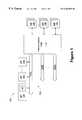
- FIG. 1is a simplified block diagram of a computer system having multiple processor buses in accordance with the present invention
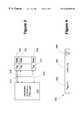
- FIG. 2is a simplified block diagram of a memory bank of the computer system of FIG. 1;
- FIG. 3is a simplified block diagram illustrating the interface between the distributed coherency filter and the DCF memory of FIG. 2;
- FIG. 4is a diagram illustrating the partitioning of an address received on the address bus of FIG. 2 .
- the computer system 100includes a plurality of processor buses 102 , each supporting one or more processors 104 . For clarity and ease of illustration, only the processors 104 associated with one of the processor buses 102 are shown. It is contemplated that the computer system 100 may have any number of processor buses 102 , with zero or more processors 104 on each processor bus 102 . One or more of the processors 104 has an associated cache memory 106 . Typically, all of the processors 104 will be of similar make and will each have an associated cache memory 106 .
- the computer system 100also includes one or more memory banks 108 . The specific number of processor buses 102 , processors 104 , and memory banks 108 is application dependent, and the present invention may be adapted for use with any number of these components.
- Interconnection logic 110couples the processor buses 102 to the memory banks 108 for communication therebetween.
- the specific construct of the interconnection logic 110is not material to the practice of the present invention, and, for clarity, is not discussed in further detail herein.
- the memory bank 108includes two main memories 200 , 201 .
- Two main memories 200 , 201are provided in the exemplary illustration, but it is contemplated that a different number of main memories 200 , 201 may be used, depending on the specific implementation.
- the main memories 200 , 201are commonly available dynamic random access memories (DRAM).
- the main memories 200 , 201are accessed by a memory address controller 202 .
- the memory address controller 202provides a memory address to the main memories 200 , 201 for accessing storage locations therein. Data used in conjunction with the accesses to the main memories 200 , 201 is held in a memory data buffer/multiplexer 204 .
- An address bus 206provides addresses to the memory address controller 202 , and data is transferred to and from the memory data buffer/multiplexer 204 on a data bus 208 .
- the memory bank 108also includes distributed coherency filter logic (DCF logic) 210 coupled to the address bus 206 in parallel with the memory address controller 202 .
- DCF logicdistributed coherency filter logic
- addresses provided on the address bus 206are generally simultaneously received by both the memory address controller 202 and the DCF logic 210 .
- the DCF logic 210interfaces with a DCF memory 212 for providing cache tag and state information (i.e., coherency information) pertaining to certain data stored in the main memories 200 , 201 .
- the nature of the interface between the DCF logic 210 and the DCF memory 212is described in greater detail in reference to FIG. 3 .
- the DCF memory 212is subdivided into blocks 300 , 302 , 304 , each of which is associated with a particular processor bus 102 .
- the block 300is associated with a first processor bus 102 A
- the block 302is associated with a second processor bus 102 B
- the block 304is associated with a final processor bus 102 N, where N is the number of processor buses in the computer system 100 .
- Each block 302 , 304 , 306maintains cache state information for the cache lines stored on its associated processor bus 102 (i.e., A, B, N, respectively).
- the DCF memory 212is a high-speed SRAM.
- the DCF memory 212is accessed based on a direct mapping of at least a portion of the address.
- An address 400includes a tag portion 402 , an index portion 404 , and a cache line size portion 406 .
- the index portion 404is used to access the DCF memory 212 , and accordingly, the number of bits in the index portion 404 determines the number of cache lines that can be addressed.
- the number of bits in the cache line size portion 406determines the number of bytes in a cache line.
- the address 400is 32 bits.
- the index portion 404is 15 bits, corresponding to 32K cache lines, and the cache line size portion 406 is 6 bits, corresponding to a cache line size of 64 bytes.
- the number of bits in the address 400 , the number of bits in the index portion 404 , and the number of bits in the cache line size portion 406are application dependent variables.
- the DCF logic 210fans out the index portion 404 of the address 400 to each of the blocks 300 , 302 , 304 in parallel to determine the status of the corresponding cache line. Because the DCF logic 210 accesses the blocks 300 , 302 , 304 in parallel, the status of the cache line on all of the processor buses 102 may be determined simultaneously. Again, a single transaction on the address bus 206 may be used to retrieve data from the main memories 200 , 201 , if required, and to check the status of the cache line on all of the processor buses 102 for that particular cache line address. Prior art techniques typically require multiple transactions to achieve such a result, thus reducing their efficiency.
- the DCF logic 210is accessed on every cacheable memory reference targeting the memory bank 108 . Based on the status retrieved from the DCF memory 212 , the DCF logic 210 issues transactions to retrieve, invalidate, or change the status of the cache line.
- the addressis provided to the DCF logic 210 and the memory address controller 202 in parallel.
- the memory address controller 202begins the process of retrieving the associated line of data from the main memories 200 , 201 , while the DCF logic 210 determines the status of any corresponding cache lines across all of the processor buses 102 . If the request misses the DCF logic 210 , a separate transaction to the memory address controller 202 is not required, and, in fact, some of the latency associated with retrieving the line of data from the main memories 200 , 201 is hidden by the parallel access.
- the original requestis completed by the memory address controller 202 and the associated memory data buffer/multiplexer 204 .
- the memory address controller 202receives the appropriate line while the DCF logic 210 updates the tag 402 in the block 302 to that of the requesting address 400 and changes the state of the line in the block 302 to owned. If another processor bus 102 indicates that the cache line is in a shared state, the state of the line in the block 302 is changed to shared and the response to the requesting processor 104 on the processor bus 102 B includes a shared indicator.
- the DCF memory 212is updated to reflect the new owner.
- the modified dataneed not be written back to the 200 , 201 , but rather, the data may be transferred from one processor bus 102 to another processor bus 102 via the interconnection logic 110 .
- an invalidation transaction or transactionsmay be multicast to the affected processor buses 102 to invalidate the cache line, and the DCF memory 212 is updated for the affected processor buses 102 , accordingly.
- the DCF memory 212is then updated to indicate that the cache line is owned by the requesting processor bus 102 B.
- the technique for maintaining cache coherency described hereinhas numerous advantages. Because the DCF logic 210 tracks cache lines using a subset of the address 400 (i.e., based on the index portion 404 ), only the most active cache lines are included. As a result, the size of the DCF memory 212 may be much smaller than the large array required for the directory based approach. Because all of the tags and states on the processor buses 102 are checked by the DCF logic 210 in parallel, the state of a particular cache line is known for the whole system 100 at once. Also, since each memory bank 108 has its own DCF logic 210 , the contention for access to any particular cache line is greatly reduced. As a result, the bandwidth is available to read and update the DCF memory 212 even during periods of high access rates, because the accesses are spread across multiple memory banks 108 .
Landscapes
- Engineering & Computer Science (AREA)
- Theoretical Computer Science (AREA)
- Physics & Mathematics (AREA)
- General Engineering & Computer Science (AREA)
- General Physics & Mathematics (AREA)
- Memory System Of A Hierarchy Structure (AREA)
Abstract
Description
Claims (39)
Priority Applications (1)
| Application Number | Priority Date | Filing Date | Title |
|---|---|---|---|
| US09/311,082US6304945B1 (en) | 1999-05-13 | 1999-05-13 | Method and apparatus for maintaining cache coherency in a computer system having multiple processor buses |
Applications Claiming Priority (1)
| Application Number | Priority Date | Filing Date | Title |
|---|---|---|---|
| US09/311,082US6304945B1 (en) | 1999-05-13 | 1999-05-13 | Method and apparatus for maintaining cache coherency in a computer system having multiple processor buses |
Publications (1)
| Publication Number | Publication Date |
|---|---|
| US6304945B1true US6304945B1 (en) | 2001-10-16 |
Family
ID=23205319
Family Applications (1)
| Application Number | Title | Priority Date | Filing Date |
|---|---|---|---|
| US09/311,082Expired - LifetimeUS6304945B1 (en) | 1999-05-13 | 1999-05-13 | Method and apparatus for maintaining cache coherency in a computer system having multiple processor buses |
Country Status (1)
| Country | Link |
|---|---|
| US (1) | US6304945B1 (en) |
Cited By (54)
| Publication number | Priority date | Publication date | Assignee | Title |
|---|---|---|---|---|
| US20030065843A1 (en)* | 2001-09-28 | 2003-04-03 | Jones Phillip M. | Next snoop predictor in a host controller |
| US20030135696A1 (en)* | 2002-01-17 | 2003-07-17 | Rankin Linda J. | Pseudo least-recently-used (PLRU) replacement method for a multi-node snoop filter |
| US6598123B1 (en)* | 2000-06-28 | 2003-07-22 | Intel Corporation | Snoop filter line replacement for reduction of back invalidates in multi-node architectures |
| US20030231649A1 (en)* | 2002-06-13 | 2003-12-18 | Awoseyi Paul A. | Dual purpose method and apparatus for performing network interface and security transactions |
| US20040019891A1 (en)* | 2002-07-25 | 2004-01-29 | Koenen David J. | Method and apparatus for optimizing performance in a multi-processing system |
| GB2403560A (en)* | 2003-07-02 | 2005-01-05 | Advanced Risc Mach Ltd | Memory bus within a coherent multi-processing system |
| US6842827B2 (en) | 2002-01-02 | 2005-01-11 | Intel Corporation | Cache coherency arrangement to enhance inbound bandwidth |
| US6868481B1 (en)* | 2000-10-31 | 2005-03-15 | Hewlett-Packard Development Company, L.P. | Cache coherence protocol for a multiple bus multiprocessor system |
| US20050144399A1 (en)* | 2003-12-24 | 2005-06-30 | Nec Corporation | Multiprocessor system, and consistency control device and consistency control method in multiprocessor system |
| US20080104330A1 (en)* | 2006-10-26 | 2008-05-01 | Freescale Semiconductor, Inc. | System and method for reporting cache coherency state retained within a cache hierarchy of a processing node |
| US20090031087A1 (en)* | 2007-07-26 | 2009-01-29 | Gaither Blaine D | Mask usable for snoop requests |
| US20090158022A1 (en)* | 2007-12-13 | 2009-06-18 | Dell Products L.P. | Snoop filter optimization |
| US20090164737A1 (en)* | 2007-12-21 | 2009-06-25 | Freescale Semiconductor, Inc. | System and method for processing potentially self-inconsistent memory transactions |
| US20100049876A1 (en)* | 2005-04-27 | 2010-02-25 | Solarflare Communications, Inc. | Packet validation in virtual network interface architecture |
| US20100057932A1 (en)* | 2006-07-10 | 2010-03-04 | Solarflare Communications Incorporated | Onload network protocol stacks |
| US20100135324A1 (en)* | 2006-11-01 | 2010-06-03 | Solarflare Communications Inc. | Driver level segmentation |
| US20100161847A1 (en)* | 2008-12-18 | 2010-06-24 | Solarflare Communications, Inc. | Virtualised interface functions |
| US20110023042A1 (en)* | 2008-02-05 | 2011-01-27 | Solarflare Communications Inc. | Scalable sockets |
| US20110029734A1 (en)* | 2009-07-29 | 2011-02-03 | Solarflare Communications Inc | Controller Integration |
| US20110087774A1 (en)* | 2009-10-08 | 2011-04-14 | Solarflare Communications Inc | Switching api |
| US20110149966A1 (en)* | 2009-12-21 | 2011-06-23 | Solarflare Communications Inc | Header Processing Engine |
| US20110173514A1 (en)* | 2003-03-03 | 2011-07-14 | Solarflare Communications, Inc. | Data protocol |
| US8533740B2 (en) | 2005-03-15 | 2013-09-10 | Solarflare Communications, Inc. | Data processing system with intercepting instructions |
| US8543729B2 (en) | 2007-11-29 | 2013-09-24 | Solarflare Communications, Inc. | Virtualised receive side scaling |
| US8612536B2 (en) | 2004-04-21 | 2013-12-17 | Solarflare Communications, Inc. | User-level stack |
| US8635353B2 (en) | 2005-06-15 | 2014-01-21 | Solarflare Communications, Inc. | Reception according to a data transfer protocol of data directed to any of a plurality of destination entities |
| US8650569B2 (en) | 2005-03-10 | 2014-02-11 | Solarflare Communications, Inc. | User-level re-initialization instruction interception |
| US8737431B2 (en) | 2004-04-21 | 2014-05-27 | Solarflare Communications, Inc. | Checking data integrity |
| US8763018B2 (en) | 2011-08-22 | 2014-06-24 | Solarflare Communications, Inc. | Modifying application behaviour |
| US8782642B2 (en) | 2005-03-15 | 2014-07-15 | Solarflare Communications, Inc. | Data processing system with data transmit capability |
| US8817784B2 (en) | 2006-02-08 | 2014-08-26 | Solarflare Communications, Inc. | Method and apparatus for multicast packet reception |
| US8855137B2 (en) | 2004-03-02 | 2014-10-07 | Solarflare Communications, Inc. | Dual-driver interface |
| US8868780B2 (en) | 2005-03-30 | 2014-10-21 | Solarflare Communications, Inc. | Data processing system with routing tables |
| US8954613B2 (en) | 2002-09-16 | 2015-02-10 | Solarflare Communications, Inc. | Network interface and protocol |
| US8959095B2 (en) | 2005-10-20 | 2015-02-17 | Solarflare Communications, Inc. | Hashing algorithm for network receive filtering |
| US8996644B2 (en) | 2010-12-09 | 2015-03-31 | Solarflare Communications, Inc. | Encapsulated accelerator |
| US9003053B2 (en) | 2011-09-22 | 2015-04-07 | Solarflare Communications, Inc. | Message acceleration |
| US9008113B2 (en) | 2010-12-20 | 2015-04-14 | Solarflare Communications, Inc. | Mapped FIFO buffering |
| US9210140B2 (en) | 2009-08-19 | 2015-12-08 | Solarflare Communications, Inc. | Remote functionality selection |
| US9258390B2 (en) | 2011-07-29 | 2016-02-09 | Solarflare Communications, Inc. | Reducing network latency |
| US9300599B2 (en) | 2013-05-30 | 2016-03-29 | Solarflare Communications, Inc. | Packet capture |
| US9384071B2 (en) | 2011-03-31 | 2016-07-05 | Solarflare Communications, Inc. | Epoll optimisations |
| US9391841B2 (en) | 2012-07-03 | 2016-07-12 | Solarflare Communications, Inc. | Fast linkup arbitration |
| US9391840B2 (en) | 2012-05-02 | 2016-07-12 | Solarflare Communications, Inc. | Avoiding delayed data |
| US9426124B2 (en) | 2013-04-08 | 2016-08-23 | Solarflare Communications, Inc. | Locked down network interface |
| US9600429B2 (en) | 2010-12-09 | 2017-03-21 | Solarflare Communications, Inc. | Encapsulated accelerator |
| US9674318B2 (en) | 2010-12-09 | 2017-06-06 | Solarflare Communications, Inc. | TCP processing for devices |
| US9686117B2 (en) | 2006-07-10 | 2017-06-20 | Solarflare Communications, Inc. | Chimney onload implementation of network protocol stack |
| US9948533B2 (en) | 2006-07-10 | 2018-04-17 | Solarflare Communitations, Inc. | Interrupt management |
| US10015104B2 (en) | 2005-12-28 | 2018-07-03 | Solarflare Communications, Inc. | Processing received data |
| US10394751B2 (en) | 2013-11-06 | 2019-08-27 | Solarflare Communications, Inc. | Programmed input/output mode |
| US10505747B2 (en) | 2012-10-16 | 2019-12-10 | Solarflare Communications, Inc. | Feed processing |
| US10742604B2 (en) | 2013-04-08 | 2020-08-11 | Xilinx, Inc. | Locked down network interface |
| US10873613B2 (en) | 2010-12-09 | 2020-12-22 | Xilinx, Inc. | TCP processing for devices |
Citations (5)
| Publication number | Priority date | Publication date | Assignee | Title |
|---|---|---|---|---|
| US5535116A (en)* | 1993-05-18 | 1996-07-09 | Stanford University | Flat cache-only multi-processor architectures |
| US5848434A (en)* | 1996-12-09 | 1998-12-08 | Intel Corporation | Method and apparatus for caching state information within a directory-based coherency memory system |
| US5897656A (en) | 1996-09-16 | 1999-04-27 | Corollary, Inc. | System and method for maintaining memory coherency in a computer system having multiple system buses |
| US6049845A (en)* | 1997-11-05 | 2000-04-11 | Unisys Corporation | System and method for providing speculative arbitration for transferring data |
| US6078997A (en)* | 1996-12-09 | 2000-06-20 | Intel Corporation | Directory-based coherency system for maintaining coherency in a dual-ported memory system |
- 1999
- 1999-05-13USUS09/311,082patent/US6304945B1/ennot_activeExpired - Lifetime
Patent Citations (5)
| Publication number | Priority date | Publication date | Assignee | Title |
|---|---|---|---|---|
| US5535116A (en)* | 1993-05-18 | 1996-07-09 | Stanford University | Flat cache-only multi-processor architectures |
| US5897656A (en) | 1996-09-16 | 1999-04-27 | Corollary, Inc. | System and method for maintaining memory coherency in a computer system having multiple system buses |
| US5848434A (en)* | 1996-12-09 | 1998-12-08 | Intel Corporation | Method and apparatus for caching state information within a directory-based coherency memory system |
| US6078997A (en)* | 1996-12-09 | 2000-06-20 | Intel Corporation | Directory-based coherency system for maintaining coherency in a dual-ported memory system |
| US6049845A (en)* | 1997-11-05 | 2000-04-11 | Unisys Corporation | System and method for providing speculative arbitration for transferring data |
Cited By (120)
| Publication number | Priority date | Publication date | Assignee | Title |
|---|---|---|---|---|
| US6598123B1 (en)* | 2000-06-28 | 2003-07-22 | Intel Corporation | Snoop filter line replacement for reduction of back invalidates in multi-node architectures |
| US6704845B2 (en) | 2000-06-28 | 2004-03-09 | Intel Corporation | Snoop filter line replacement for reduction of back invalidates in multi-node architectures |
| US20050177688A1 (en)* | 2000-10-31 | 2005-08-11 | Gaither Blain D. | Cache coherence protocol for a multiple bus multiprocessor system |
| US7373457B2 (en)* | 2000-10-31 | 2008-05-13 | Hewlett-Packard Development Company, L.P. | Cache coherence protocol for a multiple bus multiprocessor system |
| US6868481B1 (en)* | 2000-10-31 | 2005-03-15 | Hewlett-Packard Development Company, L.P. | Cache coherence protocol for a multiple bus multiprocessor system |
| US20030065843A1 (en)* | 2001-09-28 | 2003-04-03 | Jones Phillip M. | Next snoop predictor in a host controller |
| US6829665B2 (en)* | 2001-09-28 | 2004-12-07 | Hewlett-Packard Development Company, L.P. | Next snoop predictor in a host controller |
| US6842827B2 (en) | 2002-01-02 | 2005-01-11 | Intel Corporation | Cache coherency arrangement to enhance inbound bandwidth |
| US6857048B2 (en)* | 2002-01-17 | 2005-02-15 | Intel Corporation | Pseudo least-recently-used (PLRU) replacement method for a multi-node snoop filter |
| US20030135696A1 (en)* | 2002-01-17 | 2003-07-17 | Rankin Linda J. | Pseudo least-recently-used (PLRU) replacement method for a multi-node snoop filter |
| US20030231649A1 (en)* | 2002-06-13 | 2003-12-18 | Awoseyi Paul A. | Dual purpose method and apparatus for performing network interface and security transactions |
| US20040019891A1 (en)* | 2002-07-25 | 2004-01-29 | Koenen David J. | Method and apparatus for optimizing performance in a multi-processing system |
| US7143412B2 (en) | 2002-07-25 | 2006-11-28 | Hewlett-Packard Development Company, L.P. | Method and apparatus for optimizing performance in a multi-processing system |
| US9112752B2 (en) | 2002-09-16 | 2015-08-18 | Solarflare Communications, Inc. | Network interface and protocol |
| US8954613B2 (en) | 2002-09-16 | 2015-02-10 | Solarflare Communications, Inc. | Network interface and protocol |
| US9043671B2 (en) | 2003-03-03 | 2015-05-26 | Solarflare Communications, Inc. | Data protocol |
| US20110173514A1 (en)* | 2003-03-03 | 2011-07-14 | Solarflare Communications, Inc. | Data protocol |
| GB2403560A (en)* | 2003-07-02 | 2005-01-05 | Advanced Risc Mach Ltd | Memory bus within a coherent multi-processing system |
| US7162590B2 (en) | 2003-07-02 | 2007-01-09 | Arm Limited | Memory bus within a coherent multi-processing system having a main portion and a coherent multi-processing portion |
| US20050005072A1 (en)* | 2003-07-02 | 2005-01-06 | Arm Limited | Memory bus within a coherent multi-processing system |
| US20050144399A1 (en)* | 2003-12-24 | 2005-06-30 | Nec Corporation | Multiprocessor system, and consistency control device and consistency control method in multiprocessor system |
| US11182317B2 (en) | 2004-03-02 | 2021-11-23 | Xilinx, Inc. | Dual-driver interface |
| US11119956B2 (en) | 2004-03-02 | 2021-09-14 | Xilinx, Inc. | Dual-driver interface |
| US8855137B2 (en) | 2004-03-02 | 2014-10-07 | Solarflare Communications, Inc. | Dual-driver interface |
| US9690724B2 (en) | 2004-03-02 | 2017-06-27 | Solarflare Communications, Inc. | Dual-driver interface |
| US8737431B2 (en) | 2004-04-21 | 2014-05-27 | Solarflare Communications, Inc. | Checking data integrity |
| US8612536B2 (en) | 2004-04-21 | 2013-12-17 | Solarflare Communications, Inc. | User-level stack |
| US9063771B2 (en) | 2005-03-10 | 2015-06-23 | Solarflare Communications, Inc. | User-level re-initialization instruction interception |
| US8650569B2 (en) | 2005-03-10 | 2014-02-11 | Solarflare Communications, Inc. | User-level re-initialization instruction interception |
| US8533740B2 (en) | 2005-03-15 | 2013-09-10 | Solarflare Communications, Inc. | Data processing system with intercepting instructions |
| US9552225B2 (en) | 2005-03-15 | 2017-01-24 | Solarflare Communications, Inc. | Data processing system with data transmit capability |
| US8782642B2 (en) | 2005-03-15 | 2014-07-15 | Solarflare Communications, Inc. | Data processing system with data transmit capability |
| US10397103B2 (en) | 2005-03-30 | 2019-08-27 | Solarflare Communications, Inc. | Data processing system with routing tables |
| US8868780B2 (en) | 2005-03-30 | 2014-10-21 | Solarflare Communications, Inc. | Data processing system with routing tables |
| US9729436B2 (en) | 2005-03-30 | 2017-08-08 | Solarflare Communications, Inc. | Data processing system with routing tables |
| US9912665B2 (en) | 2005-04-27 | 2018-03-06 | Solarflare Communications, Inc. | Packet validation in virtual network interface architecture |
| US8380882B2 (en) | 2005-04-27 | 2013-02-19 | Solarflare Communications, Inc. | Packet validation in virtual network interface architecture |
| US10924483B2 (en) | 2005-04-27 | 2021-02-16 | Xilinx, Inc. | Packet validation in virtual network interface architecture |
| US20100049876A1 (en)* | 2005-04-27 | 2010-02-25 | Solarflare Communications, Inc. | Packet validation in virtual network interface architecture |
| US10445156B2 (en) | 2005-06-15 | 2019-10-15 | Solarflare Communications, Inc. | Reception according to a data transfer protocol of data directed to any of a plurality of destination entities |
| US8635353B2 (en) | 2005-06-15 | 2014-01-21 | Solarflare Communications, Inc. | Reception according to a data transfer protocol of data directed to any of a plurality of destination entities |
| US8645558B2 (en) | 2005-06-15 | 2014-02-04 | Solarflare Communications, Inc. | Reception according to a data transfer protocol of data directed to any of a plurality of destination entities for data extraction |
| US10055264B2 (en) | 2005-06-15 | 2018-08-21 | Solarflare Communications, Inc. | Reception according to a data transfer protocol of data directed to any of a plurality of destination entities |
| US9043380B2 (en) | 2005-06-15 | 2015-05-26 | Solarflare Communications, Inc. | Reception according to a data transfer protocol of data directed to any of a plurality of destination entities |
| US11210148B2 (en) | 2005-06-15 | 2021-12-28 | Xilinx, Inc. | Reception according to a data transfer protocol of data directed to any of a plurality of destination entities |
| US8959095B2 (en) | 2005-10-20 | 2015-02-17 | Solarflare Communications, Inc. | Hashing algorithm for network receive filtering |
| US9594842B2 (en) | 2005-10-20 | 2017-03-14 | Solarflare Communications, Inc. | Hashing algorithm for network receive filtering |
| US10015104B2 (en) | 2005-12-28 | 2018-07-03 | Solarflare Communications, Inc. | Processing received data |
| US10104005B2 (en) | 2006-01-10 | 2018-10-16 | Solarflare Communications, Inc. | Data buffering |
| US9083539B2 (en) | 2006-02-08 | 2015-07-14 | Solarflare Communications, Inc. | Method and apparatus for multicast packet reception |
| US8817784B2 (en) | 2006-02-08 | 2014-08-26 | Solarflare Communications, Inc. | Method and apparatus for multicast packet reception |
| US10382248B2 (en) | 2006-07-10 | 2019-08-13 | Solarflare Communications, Inc. | Chimney onload implementation of network protocol stack |
| US20100057932A1 (en)* | 2006-07-10 | 2010-03-04 | Solarflare Communications Incorporated | Onload network protocol stacks |
| US9948533B2 (en) | 2006-07-10 | 2018-04-17 | Solarflare Communitations, Inc. | Interrupt management |
| US8489761B2 (en) | 2006-07-10 | 2013-07-16 | Solarflare Communications, Inc. | Onload network protocol stacks |
| US9686117B2 (en) | 2006-07-10 | 2017-06-20 | Solarflare Communications, Inc. | Chimney onload implementation of network protocol stack |
| US20080104330A1 (en)* | 2006-10-26 | 2008-05-01 | Freescale Semiconductor, Inc. | System and method for reporting cache coherency state retained within a cache hierarchy of a processing node |
| US7502893B2 (en) | 2006-10-26 | 2009-03-10 | Freescale Semiconductor, Inc. | System and method for reporting cache coherency state retained within a cache hierarchy of a processing node |
| US20100135324A1 (en)* | 2006-11-01 | 2010-06-03 | Solarflare Communications Inc. | Driver level segmentation |
| US9077751B2 (en) | 2006-11-01 | 2015-07-07 | Solarflare Communications, Inc. | Driver level segmentation |
| US20090031087A1 (en)* | 2007-07-26 | 2009-01-29 | Gaither Blaine D | Mask usable for snoop requests |
| US7765363B2 (en) | 2007-07-26 | 2010-07-27 | Hewlett-Packard Development Company, L.P. | Mask usable for snoop requests |
| US8543729B2 (en) | 2007-11-29 | 2013-09-24 | Solarflare Communications, Inc. | Virtualised receive side scaling |
| US7996626B2 (en) | 2007-12-13 | 2011-08-09 | Dell Products L.P. | Snoop filter optimization |
| US20090158022A1 (en)* | 2007-12-13 | 2009-06-18 | Dell Products L.P. | Snoop filter optimization |
| US20090164737A1 (en)* | 2007-12-21 | 2009-06-25 | Freescale Semiconductor, Inc. | System and method for processing potentially self-inconsistent memory transactions |
| US9026742B2 (en) | 2007-12-21 | 2015-05-05 | Freescale Semiconductor, Inc. | System and method for processing potentially self-inconsistent memory transactions |
| US20110023042A1 (en)* | 2008-02-05 | 2011-01-27 | Solarflare Communications Inc. | Scalable sockets |
| US9304825B2 (en) | 2008-02-05 | 2016-04-05 | Solarflare Communications, Inc. | Processing, on multiple processors, data flows received through a single socket |
| US20100161847A1 (en)* | 2008-12-18 | 2010-06-24 | Solarflare Communications, Inc. | Virtualised interface functions |
| US8447904B2 (en) | 2008-12-18 | 2013-05-21 | Solarflare Communications, Inc. | Virtualised interface functions |
| US20110029734A1 (en)* | 2009-07-29 | 2011-02-03 | Solarflare Communications Inc | Controller Integration |
| US9256560B2 (en) | 2009-07-29 | 2016-02-09 | Solarflare Communications, Inc. | Controller integration |
| US9210140B2 (en) | 2009-08-19 | 2015-12-08 | Solarflare Communications, Inc. | Remote functionality selection |
| US20110087774A1 (en)* | 2009-10-08 | 2011-04-14 | Solarflare Communications Inc | Switching api |
| US8423639B2 (en) | 2009-10-08 | 2013-04-16 | Solarflare Communications, Inc. | Switching API |
| US9124539B2 (en) | 2009-12-21 | 2015-09-01 | Solarflare Communications, Inc. | Header processing engine |
| US8743877B2 (en) | 2009-12-21 | 2014-06-03 | Steven L. Pope | Header processing engine |
| US20110149966A1 (en)* | 2009-12-21 | 2011-06-23 | Solarflare Communications Inc | Header Processing Engine |
| US11134140B2 (en) | 2010-12-09 | 2021-09-28 | Xilinx, Inc. | TCP processing for devices |
| US9674318B2 (en) | 2010-12-09 | 2017-06-06 | Solarflare Communications, Inc. | TCP processing for devices |
| US9880964B2 (en) | 2010-12-09 | 2018-01-30 | Solarflare Communications, Inc. | Encapsulated accelerator |
| US9600429B2 (en) | 2010-12-09 | 2017-03-21 | Solarflare Communications, Inc. | Encapsulated accelerator |
| US9892082B2 (en) | 2010-12-09 | 2018-02-13 | Solarflare Communications Inc. | Encapsulated accelerator |
| US10515037B2 (en) | 2010-12-09 | 2019-12-24 | Solarflare Communications, Inc. | Encapsulated accelerator |
| US8996644B2 (en) | 2010-12-09 | 2015-03-31 | Solarflare Communications, Inc. | Encapsulated accelerator |
| US10873613B2 (en) | 2010-12-09 | 2020-12-22 | Xilinx, Inc. | TCP processing for devices |
| US11876880B2 (en) | 2010-12-09 | 2024-01-16 | Xilinx, Inc. | TCP processing for devices |
| US11132317B2 (en) | 2010-12-09 | 2021-09-28 | Xilinx, Inc. | Encapsulated accelerator |
| US10572417B2 (en) | 2010-12-09 | 2020-02-25 | Xilinx, Inc. | Encapsulated accelerator |
| US9800513B2 (en) | 2010-12-20 | 2017-10-24 | Solarflare Communications, Inc. | Mapped FIFO buffering |
| US9008113B2 (en) | 2010-12-20 | 2015-04-14 | Solarflare Communications, Inc. | Mapped FIFO buffering |
| US9384071B2 (en) | 2011-03-31 | 2016-07-05 | Solarflare Communications, Inc. | Epoll optimisations |
| US10671458B2 (en) | 2011-03-31 | 2020-06-02 | Xilinx, Inc. | Epoll optimisations |
| US10021223B2 (en) | 2011-07-29 | 2018-07-10 | Solarflare Communications, Inc. | Reducing network latency |
| US9456060B2 (en) | 2011-07-29 | 2016-09-27 | Solarflare Communications, Inc. | Reducing network latency |
| US10425512B2 (en) | 2011-07-29 | 2019-09-24 | Solarflare Communications, Inc. | Reducing network latency |
| US10469632B2 (en) | 2011-07-29 | 2019-11-05 | Solarflare Communications, Inc. | Reducing network latency |
| US9258390B2 (en) | 2011-07-29 | 2016-02-09 | Solarflare Communications, Inc. | Reducing network latency |
| US10713099B2 (en) | 2011-08-22 | 2020-07-14 | Xilinx, Inc. | Modifying application behaviour |
| US11392429B2 (en) | 2011-08-22 | 2022-07-19 | Xilinx, Inc. | Modifying application behaviour |
| US8763018B2 (en) | 2011-08-22 | 2014-06-24 | Solarflare Communications, Inc. | Modifying application behaviour |
| US9003053B2 (en) | 2011-09-22 | 2015-04-07 | Solarflare Communications, Inc. | Message acceleration |
| US9391840B2 (en) | 2012-05-02 | 2016-07-12 | Solarflare Communications, Inc. | Avoiding delayed data |
| US10498602B2 (en) | 2012-07-03 | 2019-12-03 | Solarflare Communications, Inc. | Fast linkup arbitration |
| US9882781B2 (en) | 2012-07-03 | 2018-01-30 | Solarflare Communications, Inc. | Fast linkup arbitration |
| US9391841B2 (en) | 2012-07-03 | 2016-07-12 | Solarflare Communications, Inc. | Fast linkup arbitration |
| US11095515B2 (en) | 2012-07-03 | 2021-08-17 | Xilinx, Inc. | Using receive timestamps to update latency estimates |
| US11108633B2 (en) | 2012-07-03 | 2021-08-31 | Xilinx, Inc. | Protocol selection in dependence upon conversion time |
| US11374777B2 (en) | 2012-10-16 | 2022-06-28 | Xilinx, Inc. | Feed processing |
| US10505747B2 (en) | 2012-10-16 | 2019-12-10 | Solarflare Communications, Inc. | Feed processing |
| US9426124B2 (en) | 2013-04-08 | 2016-08-23 | Solarflare Communications, Inc. | Locked down network interface |
| US10999246B2 (en) | 2013-04-08 | 2021-05-04 | Xilinx, Inc. | Locked down network interface |
| US10212135B2 (en) | 2013-04-08 | 2019-02-19 | Solarflare Communications, Inc. | Locked down network interface |
| US10742604B2 (en) | 2013-04-08 | 2020-08-11 | Xilinx, Inc. | Locked down network interface |
| US9300599B2 (en) | 2013-05-30 | 2016-03-29 | Solarflare Communications, Inc. | Packet capture |
| US11023411B2 (en) | 2013-11-06 | 2021-06-01 | Xilinx, Inc. | Programmed input/output mode |
| US11249938B2 (en) | 2013-11-06 | 2022-02-15 | Xilinx, Inc. | Programmed input/output mode |
| US11809367B2 (en) | 2013-11-06 | 2023-11-07 | Xilinx, Inc. | Programmed input/output mode |
| US10394751B2 (en) | 2013-11-06 | 2019-08-27 | Solarflare Communications, Inc. | Programmed input/output mode |
Similar Documents
| Publication | Publication Date | Title |
|---|---|---|
| US6304945B1 (en) | Method and apparatus for maintaining cache coherency in a computer system having multiple processor buses | |
| KR100318789B1 (en) | System and method for managing cache in a multiprocessor data processing system | |
| US8015365B2 (en) | Reducing back invalidation transactions from a snoop filter | |
| US6725341B1 (en) | Cache line pre-load and pre-own based on cache coherence speculation | |
| US5893150A (en) | Efficient allocation of cache memory space in a computer system | |
| US6289420B1 (en) | System and method for increasing the snoop bandwidth to cache tags in a multiport cache memory subsystem | |
| US7827354B2 (en) | Victim cache using direct intervention | |
| US7310708B2 (en) | Cache system with groups of lines and with coherency for both single lines and groups of lines | |
| US8171223B2 (en) | Method and system to increase concurrency and control replication in a multi-core cache hierarchy | |
| US20070136535A1 (en) | System and Method for Reducing Unnecessary Cache Operations | |
| US7305523B2 (en) | Cache memory direct intervention | |
| US20020169935A1 (en) | System of and method for memory arbitration using multiple queues | |
| US6915396B2 (en) | Fast priority determination circuit with rotating priority | |
| JP2006277762A (en) | Partitioned sparse directory for distributed shared memory multiprocessor systems | |
| US20020078304A1 (en) | System and method for allocating a directory entry for use in multiprocessor-node data processing systems | |
| US5809526A (en) | Data processing system and method for selective invalidation of outdated lines in a second level memory in response to a memory request initiated by a store operation | |
| US7281092B2 (en) | System and method of managing cache hierarchies with adaptive mechanisms | |
| US7117312B1 (en) | Mechanism and method employing a plurality of hash functions for cache snoop filtering | |
| US7325102B1 (en) | Mechanism and method for cache snoop filtering | |
| US5809537A (en) | Method and system for simultaneous processing of snoop and cache operations | |
| US6950906B2 (en) | System for and method of operating a cache | |
| US7024520B2 (en) | System and method enabling efficient cache line reuse in a computer system | |
| US6397303B1 (en) | Data processing system, cache, and method of cache management including an O state for memory-consistent cache lines | |
| US6356982B1 (en) | Dynamic mechanism to upgrade o state memory-consistent cache lines |
Legal Events
| Date | Code | Title | Description |
|---|---|---|---|
| AS | Assignment | Owner name:COMPAQ COMPUTER CORPORATION, TEXAS Free format text:ASSIGNMENT OF ASSIGNORS INTEREST;ASSIGNOR:KOENEN, DAVID J.;REEL/FRAME:009966/0643 Effective date:19990510 | |
| STCF | Information on status: patent grant | Free format text:PATENTED CASE | |
| AS | Assignment | Owner name:COMPAQ INFORMATION TECHNOLOGIES GROUP, L.P., TEXAS Free format text:ASSIGNMENT OF ASSIGNORS INTEREST;ASSIGNOR:COMPAQ COMPUTER CORPORATION;REEL/FRAME:012471/0377 Effective date:20010620 | |
| AS | Assignment | Owner name:HEWLETT-PACKARD DEVELOPMENT COMPANY, L.P., TEXAS Free format text:CHANGE OF NAME;ASSIGNOR:COMPAQ INFORMATION TECHNOLOGIES GROUP, LP;REEL/FRAME:015000/0305 Effective date:20021001 | |
| FPAY | Fee payment | Year of fee payment:4 | |
| FPAY | Fee payment | Year of fee payment:8 | |
| FPAY | Fee payment | Year of fee payment:12 | |
| AS | Assignment | Owner name:HEWLETT PACKARD ENTERPRISE DEVELOPMENT LP, TEXAS Free format text:ASSIGNMENT OF ASSIGNORS INTEREST;ASSIGNOR:HEWLETT-PACKARD DEVELOPMENT COMPANY, L.P.;REEL/FRAME:037079/0001 Effective date:20151027 |