US6304923B1 - Method for prioritizing data transfer request by comparing a latency identifier value received from an I/O device with a predetermined range of values - Google Patents
Method for prioritizing data transfer request by comparing a latency identifier value received from an I/O device with a predetermined range of valuesDownload PDFInfo
- Publication number
- US6304923B1 US6304923B1US09/172,923US17292398AUS6304923B1US 6304923 B1US6304923 B1US 6304923B1US 17292398 AUS17292398 AUS 17292398AUS 6304923 B1US6304923 B1US 6304923B1
- Authority
- US
- United States
- Prior art keywords
- latency
- values
- data transfer
- identifier
- latency identifier
- Prior art date
- Legal status (The legal status is an assumption and is not a legal conclusion. Google has not performed a legal analysis and makes no representation as to the accuracy of the status listed.)
- Expired - Lifetime
Links
Images


Classifications
- G—PHYSICS
- G06—COMPUTING OR CALCULATING; COUNTING
- G06F—ELECTRIC DIGITAL DATA PROCESSING
- G06F13/00—Interconnection of, or transfer of information or other signals between, memories, input/output devices or central processing units
- G06F13/14—Handling requests for interconnection or transfer
- G06F13/16—Handling requests for interconnection or transfer for access to memory bus
- G06F13/18—Handling requests for interconnection or transfer for access to memory bus based on priority control
- G—PHYSICS
- G06—COMPUTING OR CALCULATING; COUNTING
- G06F—ELECTRIC DIGITAL DATA PROCESSING
- G06F13/00—Interconnection of, or transfer of information or other signals between, memories, input/output devices or central processing units
- G06F13/38—Information transfer, e.g. on bus
- G06F13/42—Bus transfer protocol, e.g. handshake; Synchronisation
- G06F13/4204—Bus transfer protocol, e.g. handshake; Synchronisation on a parallel bus
- G06F13/4234—Bus transfer protocol, e.g. handshake; Synchronisation on a parallel bus being a memory bus
- G06F13/4243—Bus transfer protocol, e.g. handshake; Synchronisation on a parallel bus being a memory bus with synchronous protocol
Definitions
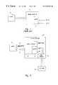
- This inventionrelates generally to controlling data transfer between a memory and a device in a computer system, and more particularly, to prioritizing service of multiple data transfer requests.
- a memory controller 10includes arbiter circuitry 12 that receives a plurality of signals indicative of requests for data transfer operations—commonly known as priority requests PREQ ⁇ -PREQ M. Each of these priority request signals corresponds to a device requesting to write data to or read data from a main memory 14 .
- Example devicesinclude a microprocessor and input/output (I/O) devices, such as peripheral component interconnect (PCI) bus devices, industry standard architecture (ISA) bus devices, integrated drive electronics (IDE) devices, accelerated graphics port (AGP) devices, small computer system interface (SCSI) devices, and universal serial bus (USB) devices, to name just a few examples.
- the arbiter 12prioritizes the various priority requests, and the memory controller 10 correspondingly initiates and controls the data transfer operations.
- the priority requestsare simply queued by the arbiter 12 , with the requested data transfer operations occurring on a first-come first-served basis.
- Certain of today's computer systemscan reorder some data transfer operations, such as by providing “read around write” capability.
- certain computer systemsallow various write operations to be reordered or combined to minimize the frequency of write operations to the memory subsystem.
- Some computer systemsprovide fixed service priorities, in which priority requests from some devices (e.g., the CPU) always receive service prior to priority requests from other devices.
- a video display devicetypically requires regular refresh of the display. The display refresh must occur regularly and timely to avoid undesirable artifacts showing on the display.
- a software-based modemrequires timely transfer of coder/decoder (CODEC) data in order to avoid corruption of the modem data.
- CDECcoder/decoder
- today's computer systemsinclude separately dedicated memories or device buffers.
- the video display in today's computer systemscommonly has a separately dedicated video memory and associated video memory controller.
- software-based modemshave a large CODEC data buffers for storing received data and transmit data.
- a methodfor controlling data transfer operations between a memory and a device in a computer system.
- the methodincludes receiving a data transfer request and a latency identifier value corresponding with a maximum time interval for servicing the data transfer request.
- the methodfurther includes waiting for a time interval no greater than the maximum time interval and then servicing the data transfer request.
- the latency identifier valuemay be successively modified and compared to a predetermined value, with servicing of the data transfer request then being initiated on the basis of that comparison.
- Multiple latency identifiers corresponding with data transfer requests from multiple computer system devicesmay be received, with one or more of the multiple latency identifiers being successively modified as time goes on. Comparing the multiple latency identifiers may be performed to identify a most urgent data transfer request. The latency identifier value corresponding with the most urgent data transfer request may then be compared to a predetermined range of values. If it is determined that this latency identifier value falls within the predetermined range of values, then servicing of the most urgent data transfer request is initiated.
- FIG. 1is a functional block diagram depicting a memory and a memory controller in accordance with the prior art.
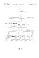
- FIG. 2is a functional block diagram depicting a computer system in accordance with an embodiment of the present invention.
- FIG. 3is a functional block diagram depicting certain details of a system controller include e computer system shown in FIG. 2 .
- FIG. 4is a functional block diagram depicting certain details of a memory controller included within the system controller shown in FIG. 3 .
- FIG. 5is a signal timing diagram depicting the sequence and timing of certain signals applied to and produced by the memory controller shown in FIG. 4 .
- FIG. 6is a part functional block, part schematic diagram depicting a portion of an arbiter circuit included within the memory controller shown in FIG. 4 .
- FIG. 7is a functional block diagram depicting a memory control state machine included within the memory controller shown in FIG. 4 .
- FIG. 8is a state diagram depicting the operations of the memory control state machine shown in FIG. 7 .
- FIG. 2shows a computer system 20 in accordance with an embodiment of the present invention.
- a microprocessor 22is coupled with a system controller 26 by a processor bus 24 that carries address, data, and control signals therebetween.
- the system controller 26includes a memory controller 28 for accessing a main memory 30 via a memory address/control bus 32 and a memory data bus 34 .
- the address/control bus 32may itself be separate, parallel address and control signal paths, or the address and control signals may be provided serially, or in some other suitable combination.
- the memory 30may include any of a wide variety of suitable memory devices.
- Example memory devicesinclude dynamic random access memory (DRAM) devices such as synchronous DRAMs, SyncLink DRAMs, or Direct RAMBUS DRAMs.
- DRAMdynamic random access memory
- the system controller 26also functions as a bridge circuit (sometimes called a North bridge) between the processor bus 24 and a system bus, such as I/O bus 36 .
- the I/O bus 36may itself be a combination of one or more bus systems with associated interface circuitry (e.g., AGP bus and PCI bus with connected SCSI and ISA bus systems).
- Multiple I/O devices 38 - 46are coupled with the I/O bus 36 .
- a data input device 38such as a keyboard, a mouse, etc., is coupled with the I/O bus 36 .
- a data output device 40such as a printer, is coupled with the I/O bus 36 .
- a visual display device 42is another data output device that is coupled with the I/O bus 36 .
- a data storage device 42such as disk drive, tape drive, CD-ROM drive, etc., is coupled with the I/O bus 36 .
- a communications device 46such as a modem, local area network (LAN) interface, etc., is coupled with the I/O bus 36 .
- expansion slots 48are provided for future accommodation of other I/O devices not selected during the original design of the computer system 20 .
- FIG. 2depicts the various I/O devices 38 - 46 as being coupled with the system controller 26 via a single shared I/O bus 36
- one or more of the I/O devicesmay have a separately dedicated interface connection to the system controller 26 .
- one or more of the I/O devices 38 - 46may be coupled with the system controller 26 via a multiple bus and bridge network.
- one or more of the I/O devices 38 - 46may be coupled with the system controller 26 partly through a shared bus system and partly through separately dedicated signal line connections. Indeed, those skilled in the art will understand the depiction of FIG. 2 to encompass any of a wide variety of suitable interconnection structures between the memory 30 , the memory controller 28 , and the I/O devices 38 - 46 .
- FIG. 3shows the connection between the memory controller 28 and a representative I/O device 50 at a device interface 52 integrated within the system controller 26 .
- the device interface 52may be a separately dedicated connection for the particular I/O device 50 , a shared bus interface, or other suitable signal interface circuitry.
- the I/O device 50desires access to the memory 30
- the device interface 52applies a data transfer request signal REQ to the memory controller 28 , as is done in conventional computer systems.
- the memory controller 28includes arbiter circuitry 54 that receives the REQ signal. In contrast with conventional computer systems, the arbiter 54 also receives a latency identification value corresponding to the particular I/O device 50 .
- the latency identification valuemay itself be provided by the I/O device 50 , may be hard-coded into the device interface 52 , or may be provided as a software ID in system configuration space, as will be understood by those skilled in the art.
- the memory controller 28also receives an address corresponding to the location in the memory 30 that the I/O device 50 wishes to access.
- the latency identification valueprovides the arbiter 54 with information concerning the maximum time interval during which the requested data transfer operation must be performed. As will be described in detail below, the memory controller 28 and arbiter 54 ensure that the requested data transfer operations occur within the maximum allowable latency period. Thus, in accordance with embodiments of the present invention, I/O devices with particular latency requirements need not have separately dedicated memory subsystems or buffers to ensure timely satisfaction of their data flow rate requirements.
- FIG. 3depicts only the single representative interface 52 between the memory controller 28 and the single representative I/O device 50 .
- a plurality of such interfacesmay be provided to handle the wide variety of data transfer operations between the main memory 30 and a plurality of other devices included within the computer system.
- a single interfacemay provide much of the signal routing for multiple devices, but with separate latency identification values for each of the devices using the interface.
- FIG. 4shows the memory controller 28 and arbiter 54 receiving a plurality of data transfer request signals REQ ⁇ -REQ N, together with associated latency identification values Latency ⁇ -Latency N and memory address locations Address ⁇ -Address N.
- the particular embodiment depicted in FIG. 4also shows the memory controller 28 receiving a priority request signal PREQ and associated Priority Address.
- the memory controller 28can include conventional priority arbitration as well as the novel latency-tagged arbitration.
- the logic circuitry associated with conventional priority request arbitration schemesis located “upstream” from the memory controller 28 .
- the memory controller 28asserts respective acknowledge signals ACK[ ⁇ :N] to the device interface 52 , and a priority acknowledge signal PACK to the conventional priority arbitration circuitry or device interface, to acknowledge the particular data transfer request being serviced and to initiate associated data transfer operations.
- a timing diagramdepicts the corresponding signal sequence and timing.
- a data transfer request signalis depicted as REQ x, which may be any of the above-described latency-tagged requests or conventional priority request (PREQ).
- the request signal REQ xwill remain asserted until service of the data transfer request has begun, which the memory controller 28 indicates with an asserted acknowledge pulse ACK x (or PACK).
- the memory controller 28also provides the various well-known memory control signals necessary to accomplish the requested data transfer operation, which are depicted in the timing diagram of FIG. 5 as MEMCYCLE x.
- a memory controller 28 in accordance with the present inventionreceives a data transfer request signal and an associated latency identification value.
- the memory controller 28is free to service other requests for data transfer operations subject to the requirement that the latency-tagged request is serviced within a maximum time interval corresponding to the latency identification value.
- Those skilled in the artwill be able to implement such a memory controller and associated arbitration scheme in any of a number of suitable ways.
- One such implementationis described in connection with FIGS. 6-8.
- FIGS. 6-8show arbitration between two latency-tagged requests REQ ⁇ and REQ 1 and a single conventional priority request PREQ.
- FIGS. 6-8show arbitration between two latency-tagged requests REQ ⁇ and REQ 1 and a single conventional priority request PREQ.
- a synchronous down counter 60loads the Latency ⁇ value at a counter input IN and produces a decremented latency value at a counter output OUT.
- Signals derived from the request signal REQ ⁇are applied to Preset and Load inputs of the counter 60 .
- REQ ⁇is deasserted, an inverter 62 then applies a corresponding asserted Preset signal, thereby maintaining the output produced by the counter 60 at a maximum, non-decrementing level.
- the Preset signalWhen, however, the REQ ⁇ signal is asserted, the Preset signal is deasserted and an asserted Load pulse is applied to the counter 60 through a synchronous latch 64 and AND gate 66 , thereby loading the latency identification value Latency ⁇ into the counter.
- the counter 60is a synchronous counter, sampling various input signal states at times referenced to a system clock signal CLK.
- a reduced frequency clock signal CLK ⁇ Mis applied to the decrementing control input DEC of the counter 60 for successively decrementing the latency value produced at the counter output OUT.
- the reduced frequency clock signal CLK ⁇ Mis preferably derived from the system clock signal CLK and has a frequency associated with a typical memory cycle time. For example, if a typical memory cycle requires M cycles of the system clock, the reduced frequency clock signal would have one-Mth the frequency of the system clock.
- Such a reduced frequency clock signalis readily provided by, for example, applying the system clock signal CLK to a conventional “divide-by-M counter,” with the “Carry” output of such counter then providing the reduced frequency clock signal CLK ⁇ M.
- the data transfer request signal REQ I and the corresponding latency identification value Latency 1are applied to a synchronous down counter and preset/load logic circuitry (not shown) of essentially the same configuration as shown in FIG. 6 and as described above in connection with REQ ⁇ .
- the latency values produced at the counter outputsare then applied to the inputs of a first comparator 68 and to the inputs of a multiplexer 70 .
- the first comparator 68produces an output signal as a function of the comparison of the latency values, which signal is then used as a selection control signal for the multiplexer 70 .
- the multiplexer 70then passes whichever of the latency values is the lowest value.
- the signal output by the first comparator 68also functions as a service priority signal Service ⁇ / ⁇ overscore (Service 1 ) ⁇ with a logic state that indicates which of the requests has current priority for service.
- a second comparator 72compares the latency value passed by the multiplexer 70 to a predetermined value, which may be selected to correspond with a lowest acceptable latency value after which the requested data transfer must be initiated. In the event the lowest latency value output by the multiplexer 70 is less than or equal to this predetermined value, the comparator 72 asserts an override priority signal OVR.
- a memory control state machine 74receives the override priority signal OVR, the service priority signal Service ⁇ overscore (/Service 1 ) ⁇ , the latency-tagged request signals REQ ⁇ and REQ 1 , and the conventional priority request signal PREQ.
- the memory control state machine 74produces the various well-known memory control signals required to access the main memory 30 (see FIGS. 4 and 5) described above.
- the memory control state machine 74also provides the acknowledge pulses ACK ⁇ , ACK 1 , PACK to acknowledge the respective requests and initiate associated data transfer operations.
- FIG. 8is a state diagram depicting the operations performed by the memory control state machine 74 of FIG. 7 .
- the particular implementation of the memory control state machine 74may be accomplished by any of a wide variety of approaches, including a microprocessor or controller executing software instructions, or hard-wired logic circuitry, to name a few examples.
- REQ ⁇is always given priority over REQ 1 , absent override priority.
- the priority request PREQis always serviced before the latency-tagged request REQ ⁇ or REQ 1 , absent override priority. Since the override functionality ensures the latency-tagged data transfer requests will be serviced in a timely fashion, providing a default preference for the conventional priority requests provides regular and timely service of these data transfer requests as well.
- the Legendidentifies the various signal state combinations A-D that result in transitions from one to another of the operating states of the memory control state machine 74 .
- the “/” positioned at the beginning of a signal nameindicates that the signal is deasserted.
- the “+” symbolindicates a logic “OR” combination of signal states, and the “.” indicates a logic “AND” combination of signal states, with conventional order-of-operations rules applying.
- the signal state combination Athen corresponds to deasserted REQ ⁇ AND deasserted REQ 1 AND deasserted PREQ.
- the signal state combination Bcorresponds to deasserted PREQ AND asserted REQ ⁇ OR asserted OVR AND asserted SRVC ⁇ .
- the signal state combination Ccorresponds to deasserted PREQ AND deasserted REQ ⁇ AND asserted REQ 1 OR asserted OVR AND asserted SRVC 1 .
- the signal state combination Dcorresponds to asserted PREQ AND deasserted OVR.
- the signal state combination Acauses the memory control state machine 74 to transition to or remain in an IDLE operating state 80 .
- the signal state combination Bcauses the memory control state machine 74 to transition to or continue in a SERVICE REQ ⁇ operating state 82 , in which the memory control state machine asserts the acknowledge signal ACK ⁇ and applies the requisite memory control signals to the memory 30 to provide the requested data transfer.
- the signal state combination Ccauses the memory control state machine 74 to transition to or continue in a SERVICE REQ 1 operating state 84 , in which the memory control state machine asserts the acknowledge signal ACK 1 and applies the requisite memory control signals to the memory 30 to provide the requested data transfer.
- the signal state combination Dcauses the memory control state machine 74 to transition to or continue in a SERVICE PREQ operating state 86 , in which the memory control state machine asserts the acknowledge signal PACK and applies the requisite memory control signals to the memory 30 to provide the requested data transfer.
- FIG. 8can be readily modified to represent the operation of the memory control state machine 74 receiving multiple latency-tagged requests REQ ⁇ -REQ N and multiple conventional priority requests PREQ ⁇ -PREQ M.
- various signal state combinations causing transition in operating statescan be modified during operation of the memory control state machine 74 to accomplish rotating default priorities (i.e., ordering memory accesses absent a latency override priority condition) or other arbitration schemes in addition to the latency-tagged arbitration method and circuitry described above.
Landscapes
- Engineering & Computer Science (AREA)
- Theoretical Computer Science (AREA)
- Physics & Mathematics (AREA)
- General Engineering & Computer Science (AREA)
- General Physics & Mathematics (AREA)
- Bus Control (AREA)
Abstract
Description
Claims (16)
Priority Applications (1)
| Application Number | Priority Date | Filing Date | Title |
|---|---|---|---|
| US09/172,923US6304923B1 (en) | 1998-10-14 | 1998-10-14 | Method for prioritizing data transfer request by comparing a latency identifier value received from an I/O device with a predetermined range of values |
Applications Claiming Priority (1)
| Application Number | Priority Date | Filing Date | Title |
|---|---|---|---|
| US09/172,923US6304923B1 (en) | 1998-10-14 | 1998-10-14 | Method for prioritizing data transfer request by comparing a latency identifier value received from an I/O device with a predetermined range of values |
Publications (1)
| Publication Number | Publication Date |
|---|---|
| US6304923B1true US6304923B1 (en) | 2001-10-16 |
Family
ID=22629767
Family Applications (1)
| Application Number | Title | Priority Date | Filing Date |
|---|---|---|---|
| US09/172,923Expired - LifetimeUS6304923B1 (en) | 1998-10-14 | 1998-10-14 | Method for prioritizing data transfer request by comparing a latency identifier value received from an I/O device with a predetermined range of values |
Country Status (1)
| Country | Link |
|---|---|
| US (1) | US6304923B1 (en) |
Cited By (21)
| Publication number | Priority date | Publication date | Assignee | Title |
|---|---|---|---|---|
| US20020188809A1 (en)* | 1999-01-19 | 2002-12-12 | Arm Limited | Memory control within data processing systems |
| US6731687B1 (en)* | 1999-10-22 | 2004-05-04 | Intel Corporation | Dynamic line balancing scheme for providing inter-packet squelch |
| US20040172500A1 (en)* | 2003-01-24 | 2004-09-02 | Hynix Semiconductor Inc. | Serial bus controller using nonvolatile ferroelectric memory |
| US20040199677A1 (en)* | 2001-12-18 | 2004-10-07 | International Business Machines Corporation | Systems, methods, and computer program products to improve performance of ported applications, such as database |
| US20040268030A1 (en)* | 2003-06-30 | 2004-12-30 | Cheung Frank Nam Go | Efficient memory controller |
| US20050182878A1 (en)* | 2004-01-19 | 2005-08-18 | Stmicroelectronics S.A. | Hierarchized arbitration method |
| US20060146722A1 (en)* | 2004-12-30 | 2006-07-06 | Jean-Francois Dube | Altering latency for network testing |
| US20060149874A1 (en)* | 2004-12-30 | 2006-07-06 | Ganasan J Prakash Subramaniam | Method and apparatus of reducing transfer latency in an SOC interconnect |
| US20060190691A1 (en)* | 2005-02-03 | 2006-08-24 | Nicolas Chauve | Die-to-die interconnect interface and protocol for stacked semiconductor dies |
| CN1299211C (en)* | 2003-12-23 | 2007-02-07 | 凌华科技股份有限公司 | System and method for realizing high-speed real-time data recording |
| US20070067507A1 (en)* | 2003-12-19 | 2007-03-22 | Shohji Ohtsubo | Recording device control apparatus |
| US20070195821A1 (en)* | 2006-02-21 | 2007-08-23 | Lih-Chung Kuo | Apparatus, system, and computer readable medium for reducing data transmission overhead |
| US20070283066A1 (en)* | 2006-06-01 | 2007-12-06 | Telefonaktiebolaget Lm Ericsson (Publ) | Arbiter diagnostic apparatus and method |
| US20080059674A1 (en)* | 2006-09-01 | 2008-03-06 | Jiaxiang Shi | Apparatus and method for chained arbitration of a plurality of inputs |
| US7373438B1 (en)* | 2002-06-13 | 2008-05-13 | Network Appliance, Inc. | System and method for reprioritizing high-latency input/output operations |
| CN100397323C (en)* | 2005-06-28 | 2008-06-25 | 群联电子股份有限公司 | Virtual USB interface flash memory storage device with high-speed peripheral component interconnection bus |
| US20080294824A1 (en)* | 2007-05-21 | 2008-11-27 | Via Technologies, Inc. | Device information management systems and methods |
| US7478025B1 (en)* | 2003-04-18 | 2009-01-13 | Unisys Corporation | System and method to support dynamic partitioning of units to a shared resource |
| US7596647B1 (en)* | 2006-09-18 | 2009-09-29 | Nvidia Corporation | Urgency based arbiter |
| US20090276269A1 (en)* | 2008-05-05 | 2009-11-05 | Oracle International Corp | Software identifier based correlation |
| US20110010511A1 (en)* | 2009-07-09 | 2011-01-13 | Kabushiki Kaisha Toshiba | Interleave control device, interleave control method, and memory system |
Citations (11)
| Publication number | Priority date | Publication date | Assignee | Title |
|---|---|---|---|---|
| US5278967A (en) | 1990-08-31 | 1994-01-11 | International Business Machines Corporation | System for providing gapless data transfer from page-mode dynamic random access memories |
| US5394541A (en)* | 1990-07-17 | 1995-02-28 | Sun Microsystems, Inc. | Programmable memory timing method and apparatus for programmably generating generic and then type specific memory timing signals |
| US5506968A (en)* | 1992-12-28 | 1996-04-09 | At&T Global Information Solutions Company | Terminating access of an agent to a shared resource when a timer, started after a low latency agent requests access, reaches a predetermined value |
| US5555383A (en) | 1994-11-07 | 1996-09-10 | International Business Machines Corporation | Peripheral component interconnect bus system having latency and shadow timers |
| WO1997029432A1 (en)* | 1996-02-09 | 1997-08-14 | Intel Corporation | Apparatus for programmably defining the access latency |
| US5818464A (en) | 1995-08-17 | 1998-10-06 | Intel Corporation | Method and apparatus for arbitrating access requests to a shared computer system memory by a graphics controller and memory controller |
| US5862355A (en)* | 1996-09-12 | 1999-01-19 | Telxon Corporation | Method and apparatus for overriding bus prioritization scheme |
| US5862353A (en) | 1997-03-25 | 1999-01-19 | International Business Machines Corporation | Systems and methods for dynamically controlling a bus |
| US5956493A (en)* | 1996-03-08 | 1999-09-21 | Advanced Micro Devices, Inc. | Bus arbiter including programmable request latency counters for varying arbitration priority |
| US5996037A (en) | 1997-06-03 | 1999-11-30 | Lsi Logic Corporation | System and method for arbitrating multi-function access to a system bus |
| US6078976A (en) | 1997-06-24 | 2000-06-20 | Matsushita Electric Industrial Co., Ltd. | Bridge device that prevents decrease in the data transfer efficiency of buses |
- 1998
- 1998-10-14USUS09/172,923patent/US6304923B1/ennot_activeExpired - Lifetime
Patent Citations (11)
| Publication number | Priority date | Publication date | Assignee | Title |
|---|---|---|---|---|
| US5394541A (en)* | 1990-07-17 | 1995-02-28 | Sun Microsystems, Inc. | Programmable memory timing method and apparatus for programmably generating generic and then type specific memory timing signals |
| US5278967A (en) | 1990-08-31 | 1994-01-11 | International Business Machines Corporation | System for providing gapless data transfer from page-mode dynamic random access memories |
| US5506968A (en)* | 1992-12-28 | 1996-04-09 | At&T Global Information Solutions Company | Terminating access of an agent to a shared resource when a timer, started after a low latency agent requests access, reaches a predetermined value |
| US5555383A (en) | 1994-11-07 | 1996-09-10 | International Business Machines Corporation | Peripheral component interconnect bus system having latency and shadow timers |
| US5818464A (en) | 1995-08-17 | 1998-10-06 | Intel Corporation | Method and apparatus for arbitrating access requests to a shared computer system memory by a graphics controller and memory controller |
| WO1997029432A1 (en)* | 1996-02-09 | 1997-08-14 | Intel Corporation | Apparatus for programmably defining the access latency |
| US5956493A (en)* | 1996-03-08 | 1999-09-21 | Advanced Micro Devices, Inc. | Bus arbiter including programmable request latency counters for varying arbitration priority |
| US5862355A (en)* | 1996-09-12 | 1999-01-19 | Telxon Corporation | Method and apparatus for overriding bus prioritization scheme |
| US5862353A (en) | 1997-03-25 | 1999-01-19 | International Business Machines Corporation | Systems and methods for dynamically controlling a bus |
| US5996037A (en) | 1997-06-03 | 1999-11-30 | Lsi Logic Corporation | System and method for arbitrating multi-function access to a system bus |
| US6078976A (en) | 1997-06-24 | 2000-06-20 | Matsushita Electric Industrial Co., Ltd. | Bridge device that prevents decrease in the data transfer efficiency of buses |
Cited By (38)
| Publication number | Priority date | Publication date | Assignee | Title |
|---|---|---|---|---|
| US20020188809A1 (en)* | 1999-01-19 | 2002-12-12 | Arm Limited | Memory control within data processing systems |
| US6684302B2 (en)* | 1999-01-19 | 2004-01-27 | Arm Limited | Bus arbitration circuit responsive to latency of access requests and the state of the memory circuit |
| US6731687B1 (en)* | 1999-10-22 | 2004-05-04 | Intel Corporation | Dynamic line balancing scheme for providing inter-packet squelch |
| US7310689B2 (en)* | 2001-12-18 | 2007-12-18 | International Business Machines Corporation | Bypassing disk I/O operations when porting a computer application from one operating system to a different operating system |
| US20040199677A1 (en)* | 2001-12-18 | 2004-10-07 | International Business Machines Corporation | Systems, methods, and computer program products to improve performance of ported applications, such as database |
| US7783787B1 (en)* | 2002-06-13 | 2010-08-24 | Netapp, Inc. | System and method for reprioritizing high-latency input/output operations |
| US7373438B1 (en)* | 2002-06-13 | 2008-05-13 | Network Appliance, Inc. | System and method for reprioritizing high-latency input/output operations |
| US7609540B2 (en)* | 2003-01-24 | 2009-10-27 | Hynix Semiconductor Inc. | Serial bus controller using nonvolatile ferroelectric memory |
| US7038929B2 (en)* | 2003-01-24 | 2006-05-02 | Hynix Semiconductor Inc. | Serial bus controller using nonvolatile ferroelectric memory |
| US20040172500A1 (en)* | 2003-01-24 | 2004-09-02 | Hynix Semiconductor Inc. | Serial bus controller using nonvolatile ferroelectric memory |
| US20070263424A1 (en)* | 2003-01-24 | 2007-11-15 | Kang Hee B | Serial bus controller using nonvolatile ferroelectric memory |
| US7478025B1 (en)* | 2003-04-18 | 2009-01-13 | Unisys Corporation | System and method to support dynamic partitioning of units to a shared resource |
| US20040268030A1 (en)* | 2003-06-30 | 2004-12-30 | Cheung Frank Nam Go | Efficient memory controller |
| US7370169B2 (en)* | 2003-06-30 | 2008-05-06 | Raytheon Company | Efficient memory controller |
| US20070067507A1 (en)* | 2003-12-19 | 2007-03-22 | Shohji Ohtsubo | Recording device control apparatus |
| US7644193B2 (en)* | 2003-12-19 | 2010-01-05 | Panasonic Corporation | Recording device control apparatus |
| CN1299211C (en)* | 2003-12-23 | 2007-02-07 | 凌华科技股份有限公司 | System and method for realizing high-speed real-time data recording |
| US20050182878A1 (en)* | 2004-01-19 | 2005-08-18 | Stmicroelectronics S.A. | Hierarchized arbitration method |
| US7315909B2 (en)* | 2004-01-19 | 2008-01-01 | Stmicroelectronics S.A. | Hierarchized arbitration method |
| US20060149874A1 (en)* | 2004-12-30 | 2006-07-06 | Ganasan J Prakash Subramaniam | Method and apparatus of reducing transfer latency in an SOC interconnect |
| US20060146722A1 (en)* | 2004-12-30 | 2006-07-06 | Jean-Francois Dube | Altering latency for network testing |
| US7593345B2 (en)* | 2004-12-30 | 2009-09-22 | Finisar Corporation | Altering latency for network testing |
| US7263566B2 (en)* | 2004-12-30 | 2007-08-28 | Qualcomm Incorporated | Method and apparatus of reducing transfer latency in an SOC interconnect |
| US20060190691A1 (en)* | 2005-02-03 | 2006-08-24 | Nicolas Chauve | Die-to-die interconnect interface and protocol for stacked semiconductor dies |
| US7743172B2 (en)* | 2005-02-03 | 2010-06-22 | Texas Instruments Incorporated | Die-to-die interconnect interface and protocol for stacked semiconductor dies |
| CN100397323C (en)* | 2005-06-28 | 2008-06-25 | 群联电子股份有限公司 | Virtual USB interface flash memory storage device with high-speed peripheral component interconnection bus |
| US20070195821A1 (en)* | 2006-02-21 | 2007-08-23 | Lih-Chung Kuo | Apparatus, system, and computer readable medium for reducing data transmission overhead |
| US20070283066A1 (en)* | 2006-06-01 | 2007-12-06 | Telefonaktiebolaget Lm Ericsson (Publ) | Arbiter diagnostic apparatus and method |
| US8468283B2 (en)* | 2006-06-01 | 2013-06-18 | Telefonaktiebolaget Lm Ericsson (Publ) | Arbiter diagnostic apparatus and method |
| US20080059674A1 (en)* | 2006-09-01 | 2008-03-06 | Jiaxiang Shi | Apparatus and method for chained arbitration of a plurality of inputs |
| US7596647B1 (en)* | 2006-09-18 | 2009-09-29 | Nvidia Corporation | Urgency based arbiter |
| US7603503B1 (en) | 2006-09-18 | 2009-10-13 | Nvidia Corporation | Efficiency based arbiter |
| US7882292B1 (en) | 2006-09-18 | 2011-02-01 | Nvidia Corporation | Urgency based arbiter |
| US20080294824A1 (en)* | 2007-05-21 | 2008-11-27 | Via Technologies, Inc. | Device information management systems and methods |
| US20090276269A1 (en)* | 2008-05-05 | 2009-11-05 | Oracle International Corp | Software identifier based correlation |
| US9953143B2 (en)* | 2008-05-05 | 2018-04-24 | Oracle International Corporation | Software identifier based correlation |
| US20110010511A1 (en)* | 2009-07-09 | 2011-01-13 | Kabushiki Kaisha Toshiba | Interleave control device, interleave control method, and memory system |
| US8145858B2 (en)* | 2009-07-09 | 2012-03-27 | Kabushiki Kaisha Toshiba | Interleave control device, interleave control method, and memory system |
Similar Documents
| Publication | Publication Date | Title |
|---|---|---|
| US6304923B1 (en) | Method for prioritizing data transfer request by comparing a latency identifier value received from an I/O device with a predetermined range of values | |
| US6073199A (en) | History-based bus arbitration with hidden re-arbitration during wait cycles | |
| US5621897A (en) | Method and apparatus for arbitrating for a bus to enable split transaction bus protocols | |
| US6266718B1 (en) | Apparatus for controlling data transfer operations between a memory and devices having respective latencies | |
| US5581782A (en) | Computer system with distributed bus arbitration scheme for symmetric and priority agents | |
| US5119480A (en) | Bus master interface circuit with transparent preemption of a data transfer operation | |
| US5590299A (en) | Multiprocessor system bus protocol for optimized accessing of interleaved storage modules | |
| US5794072A (en) | Timing method and apparatus for interleaving PIO and DMA data transfers | |
| EP0518037A2 (en) | Bus arbitration system | |
| US5717873A (en) | Deadlock avoidance mechanism and method for multiple bus topology | |
| US6134625A (en) | Method and apparatus for providing arbitration between multiple data streams | |
| US6598104B1 (en) | Smart retry system that reduces wasted bus transactions associated with master retries | |
| US6694397B2 (en) | Request queuing system for a PCI bridge | |
| JP3290650B2 (en) | Memory controller | |
| US6425037B1 (en) | Information processing system, bus arbiter, and bus controlling method | |
| JP2574976B2 (en) | Method and system for converting a central arbiter to a slave arbiter | |
| KR100480605B1 (en) | Method of controlling transmitting buffer and receiving buffer of network controller, and the network controller | |
| US5943483A (en) | Method and apparatus for controlling access to a bus in a data processing system | |
| US6247087B1 (en) | Bus system for shadowing registers | |
| US6085261A (en) | Method and apparatus for burst protocol in a data processing system | |
| US5802330A (en) | Computer system including a plurality of real time peripheral devices having arbitration control feedback mechanisms | |
| JPS6237428B2 (en) | ||
| US5748203A (en) | Computer system architecture that incorporates display memory into system memory | |
| US6026455A (en) | Architecture and method for providing guaranteed access for a retrying bus master to a data transfer bridge connecting two buses in a computer system | |
| US5983025A (en) | Computer system buffers for providing concurrency and avoid deadlock conditions between CPU accesses, local bus accesses, and memory accesses |
Legal Events
| Date | Code | Title | Description |
|---|---|---|---|
| AS | Assignment | Owner name:MICRON ELECTRONICS, INC., IDAHO Free format text:ASSIGNMENT OF ASSIGNORS INTEREST;ASSIGNOR:KLEIN, DEAN A.;REEL/FRAME:009669/0527 Effective date:19981120 | |
| AS | Assignment | Owner name:MICRON TECHNOLOGY, INC., IOWA Free format text:ASSIGNMENT OF ASSIGNORS INTEREST;ASSIGNOR:MICRON ELECTRONICS, INC.;REEL/FRAME:010763/0572 Effective date:20000317 | |
| FEPP | Fee payment procedure | Free format text:PAYOR NUMBER ASSIGNED (ORIGINAL EVENT CODE: ASPN); ENTITY STATUS OF PATENT OWNER: LARGE ENTITY | |
| STCF | Information on status: patent grant | Free format text:PATENTED CASE | |
| FEPP | Fee payment procedure | Free format text:PAYER NUMBER DE-ASSIGNED (ORIGINAL EVENT CODE: RMPN); ENTITY STATUS OF PATENT OWNER: LARGE ENTITY Free format text:PAYOR NUMBER ASSIGNED (ORIGINAL EVENT CODE: ASPN); ENTITY STATUS OF PATENT OWNER: LARGE ENTITY | |
| FPAY | Fee payment | Year of fee payment:4 | |
| FPAY | Fee payment | Year of fee payment:8 | |
| AS | Assignment | Owner name:ROUND ROCK RESEARCH, LLC,NEW YORK Free format text:ASSIGNMENT OF ASSIGNORS INTEREST;ASSIGNOR:MICRON TECHNOLOGY, INC.;REEL/FRAME:023786/0416 Effective date:20091223 Owner name:ROUND ROCK RESEARCH, LLC, NEW YORK Free format text:ASSIGNMENT OF ASSIGNORS INTEREST;ASSIGNOR:MICRON TECHNOLOGY, INC.;REEL/FRAME:023786/0416 Effective date:20091223 | |
| FPAY | Fee payment | Year of fee payment:12 |