US6304921B1 - System for serial peripheral interface with embedded addressing circuit for providing portion of an address for peripheral devices - Google Patents
System for serial peripheral interface with embedded addressing circuit for providing portion of an address for peripheral devicesDownload PDFInfo
- Publication number
- US6304921B1 US6304921B1US09/206,711US20671198AUS6304921B1US 6304921 B1US6304921 B1US 6304921B1US 20671198 AUS20671198 AUS 20671198AUS 6304921 B1US6304921 B1US 6304921B1
- Authority
- US
- United States
- Prior art keywords
- output
- input
- coupled
- flipflop
- storage elements
- Prior art date
- Legal status (The legal status is an assumption and is not a legal conclusion. Google has not performed a legal analysis and makes no representation as to the accuracy of the status listed.)
- Expired - Fee Related
Links
Images

Classifications
- G—PHYSICS
- G06—COMPUTING OR CALCULATING; COUNTING
- G06F—ELECTRIC DIGITAL DATA PROCESSING
- G06F12/00—Accessing, addressing or allocating within memory systems or architectures
- G06F12/02—Addressing or allocation; Relocation
- G06F12/06—Addressing a physical block of locations, e.g. base addressing, module addressing, memory dedication
- G06F12/0646—Configuration or reconfiguration
- G06F12/0669—Configuration or reconfiguration with decentralised address assignment
- G06F12/0676—Configuration or reconfiguration with decentralised address assignment the address being position dependent
Definitions
- the present inventionrelates in general to a microcontroller interface to peripherals and, more particularly, to a serial peripheral interface with an embedded addressing scheme.
- Microcontrollers and other microprocessorsare used in a myriad of applications to control external devices.
- a microcontrollermay control the various system functions of a vehicle.
- a microprocessorcontrols peripheral chips in a computer system.
- the microcontrollercommunicates with the external device through a serial peripheral interface (SPI).
- SPIserial peripheral interface
- the microcontrollertypically has an SPI and the external device has an SPI.
- the SPIis a standard that handles the communication protocol, signal level compatibility, data transfer, clocking, handshaking, and control and status interchange.
- the microcontrollerhas a serial output and chip select coupled to a peripheral device.
- the chip selectenables the peripheral device to receive control data at its serial input from the serial output of the microcontroller.
- the control dataconfigures or controls the peripheral device.
- the chip selectis routed to a multiplexer having one input and several selectable outputs, one for each peripheral device.
- An address signal from the microcontrollerselects one of the multiplexer outputs to enable the desired peripheral device.
- the selectable chip select solutionadds components and complexity, i.e. the multiplexer and addressing, to the overall design.
- the peripheral devicesare cascaded with the serial output of one device coupled to the serial input of the next device in the chain.
- the serial output from the microcontrolleris coupled to the serial input of the first peripheral device in the chain.
- the chip selectenables all peripheral devices.
- the peripheral devicesare addressed by the control data bits.
- the control data from the microcontrolleris serially clocked through each peripheral device in the chain so that the first control data output ends up in the last peripheral device and the last control data output ends up in the first peripheral device. If there are four cascaded peripheral devices and each device receives 8 bits of control data, then the microcontroller provides 32 bits of data over 32 clocks.
- the disadvantage of cascading the peripheral devices with a common chip selectis the communication latency of writing long strings of control data bits to address and configure the peripheral devices.
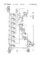
- FIG. 1is a block diagram of a microcontroller communicating with peripheral devices
- FIG. 2illustrates further detail of the serial peripheral interface portion of the peripheral device.
- an electrical system 10including a microcontroller or other electronic control circuit 12 having its serial output (SO) on conductor 14 and its chip select ( ⁇ overscore (CS) ⁇ ) output on conductor 16 .
- Microcontroller 12communicates with peripheral devices (PD) in electrical system 10 .
- PDperipheral devices
- microcontroller 12sends configuration and control data signals to the PDs to setup or modify their function or operation.
- microcontroller 12is one integrated circuit (IC) residing in a control module.
- the PDsinclude smart power drivers implemented as separate ICs also residing in the control module, or in other modules, that control vehicle functions.
- One PDcontrols the fuel injectors, another PD controls transmission solenoids, and so on.
- Conductor 14is coupled to the serial input (SI) of PD 20 .
- the SO of PD 20is coupled to the SI of PD 22 .
- the SO of PD 22is coupled to the SI of PD 24 .
- the SO of PD 24is coupled back to the SI of microcontroller 12 on conductor 26 .
- PDs 20 , 22 , and 24are like-peripheral devices in that they are physically similar in construction and operation.
- Conductor 14is also coupled to the SI of PD 30 .
- the SO of PD 30is coupled to the SI of PD 32 .
- the SO of PD 32is coupled to the SI of PD 34 .
- the SO of PD 34is coupled back to the SI of microcontroller 12 on conductor 26 .
- PDs 30 , 32 , and 34are like-peripheral devices, but may be unlike PDS 20 , 22 , and 24 .
- Conductor 14is further coupled to the SI of PD 40 .
- the SO of PD 40is coupled to the SI of PD 42 .
- the SO of PD 42is coupled to the SI of PD 44 .
- the SO of PD 44is coupled back to the SI of microcontroller 12 on conductor 26 .
- PDs 40 , 42 , and 44are like-peripheral devices, but unlike PDs 20 , 22 , and 24 and PDs 30 , 32 , and 34 .
- Conductor 14is also coupled to the SI of PD 50 , and the SO of PD 50 is coupled back to the SI of microcontroller 12 on conductor 26 .
- PD 50is unlike PDs 20 , 22 , and 24 and PDs 30 , 32 , and 34 .
- Conductor 16connects the ⁇ overscore (CS) ⁇ output of microcontroller 12 to the chip select inputs of all PDs.
- Resistor 52is a logic device coupled between the SI of PD 22 and power supply conductor 54 operating at ground potential for establishing a logic level on the SI of PD 22 .
- resistor 56is a logic device coupled between the SI of PD 24 and power supply conductor 54 for establishing a logic level on the SI of PD 24 .
- Resistors 52 and 56are pull-down devices to set a logic zero on the SI of PD 22 and PD 24 , respectively, when the SIs of PD 20 and PD 22 are not driven by the SOs of the previous PDs.
- Resistor 58is coupled between the SI of PD 32 and power supply conductor 54 .
- Resistor 60is coupled between the SI of PD 34 and power supply conductor 54 .
- Resistors 58 and 60are pull-down devices to set a logic zero on the SI of PD 32 and PD 34 , respectively, when the SIs of PD 30 and PD 32 are not driven by the SOs of the previous PDs.
- Resistor 66is coupled between the SI of PD 44 and power supply conductor 64 .
- Resistors 62 and 66are pull-up devices to set a logic one on the SI of PD 42 and PD 44 , respectively, when the SIs of PD 40 and PD 42 are not driven by the SOs of the previous PDs.
- Resistor 68operates as a pull-up on conductor 26 .
- Microcontroller 12also includes an SPI to communicate with the SPI in the PDs.
- the SPIis an 8-bit register with serial control data being input to the SI and being output from the SO of each SPI.
- PD 20includes an 8-bit device status register 70 with bit assignments as follows:
- bit 7device data start bit 1
- the device status register 70 and flipflop chain 72 - 86can be extended for additional device status/control bits and address bits.
- the contents of device status register 70are loaded into the parallel load (PL) inputs of flipflops 72 - 86 or other suitable storage elements.
- Bit 0is loaded into flipflop 72
- bit 1is loaded into flipflop 74
- bit 2is loaded into flipflop 76 , and so on.
- microcontroller 12is addressing PD 20 with a control data bit sequence “01011111”.
- the first three control data bits “010”represent the complete address of PD 20 , i.e. one address bit “0” and two device data start bits “10”.
- the next five control data bits “11111”represent the configuration and control data that set or modify the function and/or operation of PD 20 .
- Microcontroller 12places the first control data bit “0” on conductor 14 .
- the ⁇ overscore (CS) ⁇ signal on conductor 16goes to logic zero to enable the PDs.
- the system clock (SYSCLK) operating at say 2 MHzis enabled only when the ⁇ overscore (CS) ⁇ signal is logic zero.
- the first control data bitis read into flipflop 72 .
- the prior contents of flipflop 72( ⁇ overscore (data start bit 1 ) ⁇ ) is passed along to flipflop 74
- the prior contents of flipflop 74( ⁇ overscore (data start bit 1 ) ⁇ ) is passed along to flipflop 76 .
- the contents of flipflops 78 - 86remain unchanged because their clock inputs are not asserted.
- the prior contents of flipflop 76i.e. bit 2 “don't care” parallel loaded from device status register 70 ) is lost.
- the value of the first control data bit on conductor 14is also applied to one input of exclusive-NOR gate 90 .
- a second input of exclusive-NOR gate 90receives a device address bit from device address register 92 . If the value of the first control data bit on conductor 14 is the same as the device address bit then the output of exclusive-NOR gate 90 is logic one. Otherwise, the output of exclusive-NOR gate 90 is logic zero.
- bits 0 - 7represent the control data bits sent by microcontroller 12 . Note that the address bit 0 is the inverse of the data start bit 1 .
- device address register 92contains a logic zero as per table 1. The device address bit matches bit 0 on conductor 14 and the output of exclusive-NOR gate 90 is logic one. Before ⁇ overscore (CS) ⁇ is asserted, i.e. ⁇ overscore (CS) ⁇ is logic one, the Q-output of flipflop 94 is reset to logic zero. When ⁇ overscore (CS) ⁇ is logic one, the output of inverter 97 is logic zero which resets the ⁇ overscore (Q) ⁇ -output of flipflop 96 to logic one and the Q-output of flipflop 108 to logic zero.
- the logic one from the ⁇ overscore (Q) ⁇ -output of flipflop 96resets the Q-output of flipflop 102 to logic zero.
- the logic zero from the ⁇ overscore (Q) ⁇ -output of flipflop 108resets the Q-output of flipflop 110 to logic zero.
- ⁇ overscore (CS) ⁇is asserted as a logic zero, the resets are removed from flipflops 94 , 96 , and 108 allowing each to change state with the next set signal or clock signal.
- the first SYSCLK signal to the set input of flipflop 94sets its Q-output to logic one, which clocks flipflop 96 to store the logic one from exclusive-NOR gate 90 .
- the ⁇ overscore (Q) ⁇ -output of flipflop 96goes to logic zero and releases the reset on flipflop 102 .
- PDs 20 , 22 , 24 , 30 , 32 , and 34all have the ⁇ overscore (Q) ⁇ -output of flipflop 96 set to logic zero.
- the device address bit in device address register 92 of PDs 40 , 42 , 44 , and 50are set to logic one as per table 1.
- PDs 40 , 42 , 44 , and 50have the ⁇ overscore (Q) ⁇ -output of flipflop 96 set to logic one because the logic one control data bit on conductor 14 does not match the device address bit in device address register 92 of the respective devices.
- Microcontroller 12places the second control data bit (bit 1 ) with value “1” on conductor 14 .
- the second rising edge of SYSCLKshifts the second control data bit into flipflop 72 , and shifts the first control data bit into flipflop 74 , and shifts the prior contents of flipflop 74 ( ⁇ overscore (data start bit 1 ) ⁇ ) into flipflop 76 .
- device data start bit register 98is preset to logic one to identify with the device data start bit 1 of PD 20 according to table 1.
- Exclusive-NOR gate 100receives the device data start bit in register 98 and the contents of flipflop 74 , which is the first control data bit (address bit).
- the embedded addressing rule of the present embodimentdictates that the address bit is the inverse of the data start bit 1 . Therefore, at the second SYSCLK, the inputs of exclusive-NOR gate 100 are different and its output is logic zero. The Q-output of flipflop 102 remains at logic zero.
- Microcontroller 12places the third control data bit (bit 2 ) with value “0” on conductor 14 .
- the third rising edge of SYSCLKshifts the third control data bit into flipflop 72 , and shifts the second control data bit into flipflop 74 , and shifts the prior contents of flipflop 74 (address bit) into flipflop 76 .
- Exclusive-NOR gate 100receives the device data start bit in register 98 and the contents of flipflop 74 , which is the second control data bit (device data start bit 1 ). For PD 20 , the device data start bit in register 98 matches the device data start bit 1 in flipflop 74 . The output of exclusive-NOR gate 100 goes to logic one. RS flipflop 102 sets its Q-output to logic one.
- device data start bit register 104is preset to logic zero to identify with the device data start bit 2 of PD 20 according to table 1.
- Exclusive-NOR gate 106receives the device data start bit in register 104 and the contents of flipflop 72 , which by the third SYSCLK is the second control data bit (device data start bit 2 ).
- the device data start bit in register 104matches the device data start bit 2 in flipflop 72 , and the output of exclusive-NOR gate 106 goes to logic one.
- the logic one from the Q-output of flipflop 102clocks flipflop 108 and latches the logic one from its data input to its Q-output.
- the logic one on the Q-output of flipflop 108releases the reset on flipflop 110 .
- the addressing of PD 20is complete when the Q-output of flip-flop 108 goes to logic one. No other PD in the system will have its corresponding flip-flop 108 latching a logic one.
- the address “010” sent in the first three control data bits to the PDsuniquely identifies the string of PDs starting with PD 20 .
- flip-flop 110During the first three SYSCLK periods before the Q-output of flip-flop 108 switches to logic one, the reset input of flip-flop 110 is held at logic zero.
- the data input of flip-flop 110receives a fixed logic one from a positive power supply conductor operating at V DD .
- AND gate 112receives the SYSCLK on one input and the output of flipflop 110 on its other input.
- flipflop 110is held in reset, its Q-output remains at logic zero, and the output of AND gate 112 is logic zero thereby inhibiting any SYSCLK from reaching the clock inputs of flipflop 78 - 86 .
- the logic zero from the Q-output of flipflop 110also disables tri-state output driver 114 .
- flipflop 110When the address is complete and the Q-output of flipflop 108 goes to logic one, the reset input of flipflop 110 is released. The third falling edge of SYSCLK inverted by inverter 116 latches the logic one at the data input of flipflop 110 to its Q-output. With a logic one from flipflop 110 , AND gate 112 passes the SYSCLK signal to the clock inputs of flipflops 78 - 86 . The logic one from flipflop 110 also enables tri-state output driver 114 .
- PD 22receives a series of control data bits.
- the first control data bitis generated by the pull-down resistor 52 in FIG. 1 .
- the pull-down resistor 52provides a logic zero address bit for PD 22 as per table 1.
- the second and third control bitswhich are clocked into flipflops 72 - 86 of PD 22 on the fourth and fifth rising edges of SYSCLK, are the values originally loaded into flipflops 84 and 86 of PD 20 .
- the next SYSCLK periodclocks in the logic zero address bit hard-wired by resistor 52 on the SI of PD 22 into flipflop 72 of PD 22 .
- a comparisonis made of the address bit with the contents of register 92 in PD 22 as described for PD 20 .
- the next SYSCLK periodsshift in the device data start bit 1 and bit 2 from flipflops 84 and 86 of PD 20 into flipflops 74 and 76 of PD 22 as described for PD 20 .
- address bit and device data start bitsmatch the contents of registers 92 , 98 , and 104 of PD 22 , then flipflop 110 of PD 22 enables AND gate 112 of PD 22 to pass SYSCLK and to enable tri-state output buffer 114 to shift out the contents of flipflops 78 - 86 of PD 22 .
- address bit and device data start bitswill match the contents of registers 92 , 98 , and 104 of PD 22 because the resistor 52 is specifically hard-wired as a pull-down device to match the device address bit of PD 22 and flipflops 84 and 86 of PD 20 are specifically loaded with the device data start bits of PD 22 .
- a logic gate or other logic deviceinstead of a pull-up or pull-down device, could provide a logic level as the address bit to the second and later PDs in the chain.
- the embedded addressing scheme provided by the present inventionreduces the latency and overhead of writing long strings of control data to cascaded like-peripheral devices by using the pull-up or pull-down device as the address bit and the device data start bits stored in the last two flipflops of the previous PD in order to address the next PD in the chain.
- Another advantage of the present inventionis that the SPI of each PD is constructed in a similar manner.
- the address variationrelies on selecting the proper pull-up or pull-down on the SI of the PD and loading the last two flipflops of the previous PD with the appropriate device data start bit values for the next PD.
- the embedded addressing processis similar for PD 24 .
- the address bit and device data start bits sent to the SI of PD 24matches the contents of registers 92 , 98 , and 104 of PD 24 because the resistor 56 is specifically hard-wired as a pull-down device to match the device address bit of PD 24 and flipflops 84 and 86 of PD 22 are specifically loaded with the device data start bits of PD 24 .
- Microcontroller 12provides the address bit and device data start bits for the first PD in the string, i.e. PD 30 or PD 40 . If the complete address matches, then the first PD shifts out the device data start bits for the next PD in the string.
- the address bitis provided by the pull-up or pull-down device hard-wired on the SI of the next PD.
- the device data start bitsare provided by right-most flipflops of the previous PD.
- flipflop 110 of that next PDenables SYSCLK to enable tri-state output buffer 114 and shift out the contents of flipflops 78 - 86 .
- the device control bitsare clocked from conductor 14 into the SPI, the contents of the device status register 70 as parallel loaded into flipflops 72 - 86 are clocked out and sent back to microcontroller 12 .
- the device control bitsare loaded from the output of flipflops 72 - 86 into device control register 118 of each PD to control its operation after ⁇ overscore (CS) ⁇ returns to logic one.
- the device status bits sent back to microcontroller 12provide information about the PD, for example, whether a fault or error condition existed with the PD. If the PD is shut down, then that status code is sent back to microcontroller 12 to let it know that the device control bits sent to the PD are ineffective.
- the present inventionuses a microcontroller 12 to provide the address bit and device data start bits for the first PD in a string of PDs in a chain.
- Multiple chains of PDsoperate under control of a single serial output and chip select of the microcontroller.
- Each chain of PDshas like-peripheral devices.
- Each PDincludes a string of flipflops. The contents of a device status register are loaded into the flipflops. If the complete address matches, then the first PD shifts out the device data start bits for the next PD in the string.
- the address bit for the next PDis provided by the pull-up or pull-down device hard-wired on the SI of the next PD.
- the device data start bits for the next PDare provided by right-most flipflops of the previous PD. If the address bit and device data start bits match the contents of the device registers of the next PD, then that next PD enables SYSCLK to shift out the contents of flipflops. As the device control bits are clocked from conductor 14 into the SPI, the contents of the device status register are clocked out and sent back to the microcontroller.
- the present inventionprovides for like-peripheral devices to be cascaded while unlike-devices are addressed in parallel.
Landscapes
- Engineering & Computer Science (AREA)
- Theoretical Computer Science (AREA)
- Physics & Mathematics (AREA)
- General Engineering & Computer Science (AREA)
- General Physics & Mathematics (AREA)
- Information Transfer Systems (AREA)
Abstract
Description
| TABLE 1 | |||
| Address | Data Start Bits | Peripheral Data Bits | |
| Devices | bit0 | bit1 | bit2 | bit3 | bit4 | bit5 | bit6 | bit7 |
| 0 | 1 | 0 | data | data | data | data | ||
| PD | ||||||||
| 22 | 0 | 1 | 0 | data | data | data | data | |
| PD | ||||||||
| 24 | 0 | 1 | 0 | data | data | data | data | |
| PD | ||||||||
| 30 | 0 | 1 | 1 | data | data | data | data | |
| PD | ||||||||
| 32 | 0 | 1 | 1 | data | data | data | data | |
| PD | ||||||||
| 34 | 0 | 1 | 1 | data | data | data | data | |
| PD | ||||||||
| 40 | 1 | 0 | 0 | data | data | data | data | |
| PD | ||||||||
| 42 | 1 | 0 | 0 | data | data | data | data | |
| PD | ||||||||
| 44 | 1 | 0 | 0 | data | data | data | data | |
| PD | ||||||||
| 50 | 1 | 0 | 1 | data | data | data | data | data |
Claims (18)
Priority Applications (1)
| Application Number | Priority Date | Filing Date | Title |
|---|---|---|---|
| US09/206,711US6304921B1 (en) | 1998-12-07 | 1998-12-07 | System for serial peripheral interface with embedded addressing circuit for providing portion of an address for peripheral devices |
Applications Claiming Priority (1)
| Application Number | Priority Date | Filing Date | Title |
|---|---|---|---|
| US09/206,711US6304921B1 (en) | 1998-12-07 | 1998-12-07 | System for serial peripheral interface with embedded addressing circuit for providing portion of an address for peripheral devices |
Publications (1)
| Publication Number | Publication Date |
|---|---|
| US6304921B1true US6304921B1 (en) | 2001-10-16 |
Family
ID=22767608
Family Applications (1)
| Application Number | Title | Priority Date | Filing Date |
|---|---|---|---|
| US09/206,711Expired - Fee RelatedUS6304921B1 (en) | 1998-12-07 | 1998-12-07 | System for serial peripheral interface with embedded addressing circuit for providing portion of an address for peripheral devices |
Country Status (1)
| Country | Link |
|---|---|
| US (1) | US6304921B1 (en) |
Cited By (58)
| Publication number | Priority date | Publication date | Assignee | Title |
|---|---|---|---|---|
| US20020141438A1 (en)* | 2001-02-09 | 2002-10-03 | Smith J. Howard | Data communication controller and method |
| US20030123473A1 (en)* | 2001-12-28 | 2003-07-03 | Masahito Satoh | Variable time division multiplex transmission system |
| US20030128702A1 (en)* | 2001-12-28 | 2003-07-10 | Masahito Satoh | Communication method and apparatus for assigning device identifier |
| US20040037220A1 (en)* | 2001-12-14 | 2004-02-26 | Andreas Junger | Method of data transmission and a transmission and reception device in a distributed system |
| DE10336807A1 (en)* | 2003-08-11 | 2005-03-17 | Siemens Ag | Serial interface functionality expansion method for e.g. mobile radio frequency devices, uses chip selection line for programming subsequent units via main units |
| US20050114553A1 (en)* | 2001-04-02 | 2005-05-26 | Lada Henry F. | Handheld option pack interface |
| US20070076502A1 (en)* | 2005-09-30 | 2007-04-05 | Pyeon Hong B | Daisy chain cascading devices |
| US20070076479A1 (en)* | 2005-09-30 | 2007-04-05 | Mosaid Technologies Incorporated | Multiple independent serial link memory |
| US20070153576A1 (en)* | 2005-09-30 | 2007-07-05 | Hakjune Oh | Memory with output control |
| US20070230253A1 (en)* | 2006-03-29 | 2007-10-04 | Jin-Ki Kim | Non-volatile semiconductor memory with page erase |
| US20070233917A1 (en)* | 2006-03-28 | 2007-10-04 | Mosaid Technologies Incorporated | Apparatus and method for establishing device identifiers for serially interconnected devices |
| US20070233903A1 (en)* | 2006-03-28 | 2007-10-04 | Hong Beom Pyeon | Daisy chain cascade configuration recognition technique |
| US20070234071A1 (en)* | 2006-03-28 | 2007-10-04 | Mosaid Technologies Incorporated | Asynchronous ID generation |
| US20070233939A1 (en)* | 2006-03-31 | 2007-10-04 | Mosaid Technologies Incorporated | Flash memory system control scheme |
| US20080049505A1 (en)* | 2006-08-22 | 2008-02-28 | Mosaid Technologies Incorporated | Scalable memory system |
| US20080080492A1 (en)* | 2006-09-29 | 2008-04-03 | Mosaid Technologies Incorporated | Packet based ID generation for serially interconnected devices |
| US20080123423A1 (en)* | 2006-11-27 | 2008-05-29 | Mosaid Technologies Incorporated | Non-volatile memory serial core architecture |
| US20080140948A1 (en)* | 2006-12-06 | 2008-06-12 | Mosaid Technologies Incorporated | Apparatus and method for producing device identifiers for serially interconnected devices of mixed type |
| US20080140899A1 (en)* | 2006-12-06 | 2008-06-12 | Mosaid Technologies Incorporated | Address assignment and type recognition of serially interconnected memory devices of mixed type |
| US20080137467A1 (en)* | 2006-12-06 | 2008-06-12 | Mosaid Technologies Incorporated | Apparatus and method for capturing serial input data |
| US20080137461A1 (en)* | 2006-12-12 | 2008-06-12 | Hong Beom Pyeon | Memory system and method with serial and parallel modes |
| US20080140916A1 (en)* | 2006-12-06 | 2008-06-12 | Mosaid Technologies Incorporated | System and method of operating memory devices of mixed type |
| US20080155179A1 (en)* | 2006-12-06 | 2008-06-26 | Mosaid Technologies Incorporated | Apparatus and method for producing ids for interconnected devices of mixed type |
| US20080155185A1 (en)* | 2006-12-20 | 2008-06-26 | Jin-Ki Kim | Hybrid solid-state memory system having volatile and non-volatile memory |
| US20080155219A1 (en)* | 2006-12-20 | 2008-06-26 | Mosaid Technologies Incorporated | Id generation apparatus and method for serially interconnected devices |
| US20080168296A1 (en)* | 2006-12-06 | 2008-07-10 | Hakjune Oh | Apparatus and method for communicating with semiconductor devices of a serial interconnection |
| US20080181214A1 (en)* | 2006-12-06 | 2008-07-31 | Mosaid Technologies Incorporated | Apparatus and method for producing device identifiers for serially interconnected devices of mixed type |
| US20080183928A1 (en)* | 2007-01-29 | 2008-07-31 | Microsemi Corp. - Analog Mixed Signal Group Ltd. | Addressable Serial Peripheral Interface |
| US20080192649A1 (en)* | 2006-12-06 | 2008-08-14 | Mosaid Technologies Incorporated | Apparatus and method for producing identifiers regardless of mixed device type in a serial interconnection |
| US20080195613A1 (en)* | 2007-02-13 | 2008-08-14 | Mosaid Technologies Incorporated | Apparatus and method for identifying device types of series-connected devices of mixed type |
| US20080198682A1 (en)* | 2007-02-16 | 2008-08-21 | Mosaid Technologies Incorporated | Semiconductor device and method for selection and de-selection of memory devices interconnected in series |
| US20080201496A1 (en)* | 2007-02-16 | 2008-08-21 | Peter Gillingham | Reduced pin count interface |
| US20080209110A1 (en)* | 2007-02-22 | 2008-08-28 | Mosaid Technologies Incorporated | Apparatus and method of page program operation for memory devices with mirror back-up of data |
| US20080209108A1 (en)* | 2007-02-22 | 2008-08-28 | Hong Beom Pyeon | System and method of page buffer operation for memory devices |
| US20080205187A1 (en)* | 2007-02-22 | 2008-08-28 | Mosaid Technologies Incorporated | Data flow control in multiple independent port |
| US20080226004A1 (en)* | 2007-03-12 | 2008-09-18 | Hakjune Oh | Methods and apparatus for clock signal synchronization in a configuration of series-connected semiconductor devices |
| US20080297805A1 (en)* | 2006-12-21 | 2008-12-04 | Honeywell International, Inc. | Spectral balancing system and method for reducing noise in fiber optic gyroscopes |
| US20090021992A1 (en)* | 2007-07-18 | 2009-01-22 | Hakjune Oh | Memory with data control |
| US20090129184A1 (en)* | 2007-11-15 | 2009-05-21 | Mosaid Technologies Incorporated | Methods and systems for failure isolation and data recovery in a configuration of series-connected semiconductor devices |
| US20090138768A1 (en)* | 2007-11-23 | 2009-05-28 | Mosaid Technologies Incorporated | Data channel test apparatus and method thereof |
| US20090154285A1 (en)* | 2007-12-14 | 2009-06-18 | Mosaid Technologies Incorporated | Memory controller with flexible data alignment to clock |
| US20090154629A1 (en)* | 2007-12-14 | 2009-06-18 | Mosaid Technologies Incorporated | Clock reproducing and timing method in a system having a plurality of devices |
| US20090161451A1 (en)* | 2007-12-20 | 2009-06-25 | Mosaid Technologies Incorporated | Dual function compatible non-volatile memory device |
| US20090175081A1 (en)* | 2008-01-07 | 2009-07-09 | Mosaid Technologies Incorporated | Nand flash memory having multiple cell substrates |
| US20100011174A1 (en)* | 2008-07-08 | 2010-01-14 | Mosaid Technologies Incorporated | Mixed data rates in memory devices and systems |
| US20100083027A1 (en)* | 2008-09-30 | 2010-04-01 | Mosaid Technologies Incorporated | Serial-connected memory system with output delay adjustment |
| US20100083028A1 (en)* | 2008-09-30 | 2010-04-01 | Mosaid Technologies Incorporated | Serial-connected memory system with duty cycle correction |
| US20100117788A1 (en)* | 2007-04-26 | 2010-05-13 | Freescale Semiconductor, Inc. | Diagnosis for mixed signal device for use in a distributed system |
| US20100157715A1 (en)* | 2008-12-18 | 2010-06-24 | Hong-Beom Pyeon | Semiconductor device with main memory unit and auxiliary memory unit requiring preset operation |
| US20100161877A1 (en)* | 2008-12-18 | 2010-06-24 | Hong Beom Pyeon | Device and method for transferring data to a non-volatile memory device |
| US7747833B2 (en) | 2005-09-30 | 2010-06-29 | Mosaid Technologies Incorporated | Independent link and bank selection |
| US20110016279A1 (en)* | 2009-07-16 | 2011-01-20 | Mosaid Technologies Incorporated | Simultaneous read and write data transfer |
| US7904639B2 (en) | 2006-08-22 | 2011-03-08 | Mosaid Technologies Incorporated | Modular command structure for memory and memory system |
| US8594110B2 (en) | 2008-01-11 | 2013-11-26 | Mosaid Technologies Incorporated | Ring-of-clusters network topologies |
| US20140089548A1 (en)* | 2012-09-26 | 2014-03-27 | Ronald Norman Prusia | Systems, Methods, and Articles of Manufacture To Stream Data |
| US20140115212A1 (en)* | 2012-10-23 | 2014-04-24 | Seiko Epson Corporation | Serial communication circuit, integrated circuit device, physical quantity measuring device, electronic apparatus, moving object, and serial communication method |
| CN106021044A (en)* | 2016-05-10 | 2016-10-12 | 中国电子科技集团公司第三十八研究所 | Reusable SPI (Serial Peripheral Interface) bus protocol module verification environment platform and verification method thereof |
| US11948629B2 (en) | 2005-09-30 | 2024-04-02 | Mosaid Technologies Incorporated | Non-volatile memory device with concurrent bank operations |
Citations (11)
| Publication number | Priority date | Publication date | Assignee | Title |
|---|---|---|---|---|
| US3881174A (en)* | 1974-01-18 | 1975-04-29 | Process Computer Systems Inc | Peripheral interrupt apparatus for digital computer system |
| US4815034A (en)* | 1981-03-18 | 1989-03-21 | Mackey Timothy I | Dynamic memory address system for I/O devices |
| US4918657A (en)* | 1987-03-18 | 1990-04-17 | Nec Corporation | Semiconductor memory device provided with an improved precharge and enable control circuit |
| US5404460A (en)* | 1994-01-28 | 1995-04-04 | Vlsi Technology, Inc. | Method for configuring multiple identical serial I/O devices to unique addresses through a serial bus |
| US5408612A (en)* | 1992-09-09 | 1995-04-18 | Digital Equipment Corporation | Microprocessor system for selectively accessing a processor internal register when the processor has control of the bus and partial address identifying the register |
| US5475854A (en)* | 1994-01-28 | 1995-12-12 | Vlsi Technology, Inc. | Serial bus I/O system and method for serializing interrupt requests and DMA requests in a computer system |
| US5828899A (en)* | 1996-01-04 | 1998-10-27 | Compaq Computer Corporation | System for peripheral devices recursively generating unique addresses based on the number of devices connected dependent upon the relative position to the port |
| US5864715A (en)* | 1996-06-21 | 1999-01-26 | Emc Corporation | System for automatically terminating a daisy-chain peripheral bus with either single-ended or differential termination network depending on peripheral bus signals and peripheral device interfaces |
| US5922056A (en)* | 1997-03-03 | 1999-07-13 | International Business Machines Corporation | Computer system with peripheral device characteristic sensing and automatic communications speed setting |
| US5926648A (en)* | 1996-08-22 | 1999-07-20 | Zilog, Inc. | I/O port and RAM memory addressing technique |
| US5991830A (en)* | 1996-01-04 | 1999-11-23 | Compaq Computer Corp. | Apparatus and method for coupling multiple peripheral devices to a single port of a computer |
- 1998
- 1998-12-07USUS09/206,711patent/US6304921B1/ennot_activeExpired - Fee Related
Patent Citations (11)
| Publication number | Priority date | Publication date | Assignee | Title |
|---|---|---|---|---|
| US3881174A (en)* | 1974-01-18 | 1975-04-29 | Process Computer Systems Inc | Peripheral interrupt apparatus for digital computer system |
| US4815034A (en)* | 1981-03-18 | 1989-03-21 | Mackey Timothy I | Dynamic memory address system for I/O devices |
| US4918657A (en)* | 1987-03-18 | 1990-04-17 | Nec Corporation | Semiconductor memory device provided with an improved precharge and enable control circuit |
| US5408612A (en)* | 1992-09-09 | 1995-04-18 | Digital Equipment Corporation | Microprocessor system for selectively accessing a processor internal register when the processor has control of the bus and partial address identifying the register |
| US5404460A (en)* | 1994-01-28 | 1995-04-04 | Vlsi Technology, Inc. | Method for configuring multiple identical serial I/O devices to unique addresses through a serial bus |
| US5475854A (en)* | 1994-01-28 | 1995-12-12 | Vlsi Technology, Inc. | Serial bus I/O system and method for serializing interrupt requests and DMA requests in a computer system |
| US5828899A (en)* | 1996-01-04 | 1998-10-27 | Compaq Computer Corporation | System for peripheral devices recursively generating unique addresses based on the number of devices connected dependent upon the relative position to the port |
| US5991830A (en)* | 1996-01-04 | 1999-11-23 | Compaq Computer Corp. | Apparatus and method for coupling multiple peripheral devices to a single port of a computer |
| US5864715A (en)* | 1996-06-21 | 1999-01-26 | Emc Corporation | System for automatically terminating a daisy-chain peripheral bus with either single-ended or differential termination network depending on peripheral bus signals and peripheral device interfaces |
| US5926648A (en)* | 1996-08-22 | 1999-07-20 | Zilog, Inc. | I/O port and RAM memory addressing technique |
| US5922056A (en)* | 1997-03-03 | 1999-07-13 | International Business Machines Corporation | Computer system with peripheral device characteristic sensing and automatic communications speed setting |
Cited By (190)
| Publication number | Priority date | Publication date | Assignee | Title |
|---|---|---|---|---|
| US20020141438A1 (en)* | 2001-02-09 | 2002-10-03 | Smith J. Howard | Data communication controller and method |
| US20050114553A1 (en)* | 2001-04-02 | 2005-05-26 | Lada Henry F. | Handheld option pack interface |
| US20040037220A1 (en)* | 2001-12-14 | 2004-02-26 | Andreas Junger | Method of data transmission and a transmission and reception device in a distributed system |
| US20030123473A1 (en)* | 2001-12-28 | 2003-07-03 | Masahito Satoh | Variable time division multiplex transmission system |
| US20030128702A1 (en)* | 2001-12-28 | 2003-07-10 | Masahito Satoh | Communication method and apparatus for assigning device identifier |
| US7830906B2 (en)* | 2001-12-28 | 2010-11-09 | Texas Instruments Incorporated | Variable time division multiplex transmission system |
| US20080069151A1 (en)* | 2001-12-28 | 2008-03-20 | Texas Instruments Incorporated | Variable time division multiplex transmission system |
| DE10336807A1 (en)* | 2003-08-11 | 2005-03-17 | Siemens Ag | Serial interface functionality expansion method for e.g. mobile radio frequency devices, uses chip selection line for programming subsequent units via main units |
| DE10336807B4 (en)* | 2003-08-11 | 2010-12-09 | Palm, Inc. (n.d.Ges. d. Staates Delaware), Sunnyvale | Method and device for extending the functionality of a serial interface and a mobile device using the method and a mobile device comprising the device |
| US20070109833A1 (en)* | 2005-09-30 | 2007-05-17 | Pyeon Hong B | Daisy chain cascading devices |
| US20070076502A1 (en)* | 2005-09-30 | 2007-04-05 | Pyeon Hong B | Daisy chain cascading devices |
| US9240227B2 (en) | 2005-09-30 | 2016-01-19 | Conversant Intellectual Property Management Inc. | Daisy chain cascading devices |
| US8427897B2 (en) | 2005-09-30 | 2013-04-23 | Mosaid Technologies Incorporated | Memory with output control |
| US7515471B2 (en) | 2005-09-30 | 2009-04-07 | Mosaid Technologies Incorporated | Memory with output control |
| US11600323B2 (en) | 2005-09-30 | 2023-03-07 | Mosaid Technologies Incorporated | Non-volatile memory device with concurrent bank operations |
| US20070153576A1 (en)* | 2005-09-30 | 2007-07-05 | Hakjune Oh | Memory with output control |
| US8738879B2 (en) | 2005-09-30 | 2014-05-27 | Conversant Intellectual Property Managament Inc. | Independent link and bank selection |
| US8000144B2 (en) | 2005-09-30 | 2011-08-16 | Mosaid Technologies Incorporated | Method and system for accessing a flash memory device |
| US20080279003A1 (en)* | 2005-09-30 | 2008-11-13 | Mosaid Technologies Incorporated | Multiple independent serial link memory |
| US11948629B2 (en) | 2005-09-30 | 2024-04-02 | Mosaid Technologies Incorporated | Non-volatile memory device with concurrent bank operations |
| US20070076479A1 (en)* | 2005-09-30 | 2007-04-05 | Mosaid Technologies Incorporated | Multiple independent serial link memory |
| US8654601B2 (en) | 2005-09-30 | 2014-02-18 | Mosaid Technologies Incorporated | Memory with output control |
| US9230654B2 (en) | 2005-09-30 | 2016-01-05 | Conversant Intellectual Property Management Inc. | Method and system for accessing a flash memory device |
| US7826294B2 (en) | 2005-09-30 | 2010-11-02 | Mosaid Technologies Incorporated | Memory with output control |
| US7652922B2 (en) | 2005-09-30 | 2010-01-26 | Mosaid Technologies Incorporated | Multiple independent serial link memory |
| US20110179245A1 (en)* | 2005-09-30 | 2011-07-21 | Mosaid Technologies Incorporated | Independent link and bank selection |
| US8199598B2 (en) | 2005-09-30 | 2012-06-12 | Mosaid Technologies Incorporated | Memory with output control |
| US8743610B2 (en) | 2005-09-30 | 2014-06-03 | Conversant Intellectual Property Management Inc. | Method and system for accessing a flash memory device |
| US20100199057A1 (en)* | 2005-09-30 | 2010-08-05 | Mosaid Technologies Incorporated | Independent link and bank selection |
| US20100182838A1 (en)* | 2005-09-30 | 2010-07-22 | Mosaid Technologies Incorporated | Flash memory device with data output control |
| US7945755B2 (en) | 2005-09-30 | 2011-05-17 | Mosaid Technologies Incorporated | Independent link and bank selection |
| US7747833B2 (en) | 2005-09-30 | 2010-06-29 | Mosaid Technologies Incorporated | Independent link and bank selection |
| US7719892B2 (en) | 2005-09-30 | 2010-05-18 | Mosaid Technologies Incorproated | Flash memory device with data output control |
| US8285960B2 (en) | 2005-09-30 | 2012-10-09 | Mosaid Technologies Incorporated | Independent link and bank selection |
| US8069328B2 (en) | 2006-03-28 | 2011-11-29 | Mosaid Technologies Incorporated | Daisy chain cascade configuration recognition technique |
| US20070234071A1 (en)* | 2006-03-28 | 2007-10-04 | Mosaid Technologies Incorporated | Asynchronous ID generation |
| US8364861B2 (en) | 2006-03-28 | 2013-01-29 | Mosaid Technologies Incorporated | Asynchronous ID generation |
| US8335868B2 (en) | 2006-03-28 | 2012-12-18 | Mosaid Technologies Incorporated | Apparatus and method for establishing device identifiers for serially interconnected devices |
| US20070233917A1 (en)* | 2006-03-28 | 2007-10-04 | Mosaid Technologies Incorporated | Apparatus and method for establishing device identifiers for serially interconnected devices |
| US20070233903A1 (en)* | 2006-03-28 | 2007-10-04 | Hong Beom Pyeon | Daisy chain cascade configuration recognition technique |
| US8559237B2 (en) | 2006-03-29 | 2013-10-15 | Mosaid Technologies Incorporated | Non-volatile semiconductor memory with page erase |
| US20110069551A1 (en)* | 2006-03-29 | 2011-03-24 | Mosaid Technologies Incorporated | Non-Volatile Semiconductor Memory with Page Erase |
| US7872921B2 (en) | 2006-03-29 | 2011-01-18 | Mosaid Technologies Incorporated | Non-volatile semiconductor memory with page erase |
| US20070230253A1 (en)* | 2006-03-29 | 2007-10-04 | Jin-Ki Kim | Non-volatile semiconductor memory with page erase |
| US7995401B2 (en) | 2006-03-29 | 2011-08-09 | Mosaid Technologies Incorporated | Non-volatile semiconductor memory with page erase |
| US8213240B2 (en) | 2006-03-29 | 2012-07-03 | Mosaid Technologies Incorporated | Non-volatile semiconductor memory with page erase |
| US7551492B2 (en) | 2006-03-29 | 2009-06-23 | Mosaid Technologies, Inc. | Non-volatile semiconductor memory with page erase |
| US20070233939A1 (en)* | 2006-03-31 | 2007-10-04 | Mosaid Technologies Incorporated | Flash memory system control scheme |
| US20100325353A1 (en)* | 2006-03-31 | 2010-12-23 | Mosaid Technologies Incorporated | Flash memory system control scheme |
| US7802064B2 (en) | 2006-03-31 | 2010-09-21 | Mosaid Technologies Incorporated | Flash memory system control scheme |
| US8671252B2 (en) | 2006-08-22 | 2014-03-11 | Mosaid Technologies Incorporated | Scalable memory system |
| US20080049505A1 (en)* | 2006-08-22 | 2008-02-28 | Mosaid Technologies Incorporated | Scalable memory system |
| US7904639B2 (en) | 2006-08-22 | 2011-03-08 | Mosaid Technologies Incorporated | Modular command structure for memory and memory system |
| US8407395B2 (en) | 2006-08-22 | 2013-03-26 | Mosaid Technologies Incorporated | Scalable memory system |
| US20110131383A1 (en)* | 2006-08-22 | 2011-06-02 | Mosaid Technologies Incorporated | Modular command structure for memory and memory system |
| US8700818B2 (en) | 2006-09-29 | 2014-04-15 | Mosaid Technologies Incorporated | Packet based ID generation for serially interconnected devices |
| US20080080492A1 (en)* | 2006-09-29 | 2008-04-03 | Mosaid Technologies Incorporated | Packet based ID generation for serially interconnected devices |
| US8879351B2 (en) | 2006-11-27 | 2014-11-04 | Conversant Intellectual Property Management Inc. | Non-volatile memory bank and page buffer therefor |
| US20110013455A1 (en)* | 2006-11-27 | 2011-01-20 | Mosaid Technologies Incorporated | Non-volatile memory serial core architecture |
| US20080123423A1 (en)* | 2006-11-27 | 2008-05-29 | Mosaid Technologies Incorporated | Non-volatile memory serial core architecture |
| US7817470B2 (en) | 2006-11-27 | 2010-10-19 | Mosaid Technologies Incorporated | Non-volatile memory serial core architecture |
| US8289805B2 (en) | 2006-11-27 | 2012-10-16 | Mosaid Technologies Incorporated | Non-volatile memory bank and page buffer therefor |
| US20080168296A1 (en)* | 2006-12-06 | 2008-07-10 | Hakjune Oh | Apparatus and method for communicating with semiconductor devices of a serial interconnection |
| US7925854B2 (en) | 2006-12-06 | 2011-04-12 | Mosaid Technologies Incorporated | System and method of operating memory devices of mixed type |
| US8694692B2 (en) | 2006-12-06 | 2014-04-08 | Mosaid Technologies Incorporated | Apparatus and method for producing device identifiers for serially interconnected devices of mixed type |
| US8230147B2 (en) | 2006-12-06 | 2012-07-24 | Mosaid Technologies Incorporated | Apparatus and method for communicating with semiconductor devices of a serial interconnection |
| US8271758B2 (en) | 2006-12-06 | 2012-09-18 | Mosaid Technologies Incorporated | Apparatus and method for producing IDS for interconnected devices of mixed type |
| US8331361B2 (en) | 2006-12-06 | 2012-12-11 | Mosaid Technologies Incorporated | Apparatus and method for producing device identifiers for serially interconnected devices of mixed type |
| US7752364B2 (en) | 2006-12-06 | 2010-07-06 | Mosaid Technologies Incorporated | Apparatus and method for communicating with semiconductor devices of a serial interconnection |
| US20080192649A1 (en)* | 2006-12-06 | 2008-08-14 | Mosaid Technologies Incorporated | Apparatus and method for producing identifiers regardless of mixed device type in a serial interconnection |
| US8195839B2 (en) | 2006-12-06 | 2012-06-05 | Mosaid Technologies Incorporated | Apparatus and method for producing identifiers regardless of mixed device type in a serial interconnection |
| US20080181214A1 (en)* | 2006-12-06 | 2008-07-31 | Mosaid Technologies Incorporated | Apparatus and method for producing device identifiers for serially interconnected devices of mixed type |
| US8433874B2 (en) | 2006-12-06 | 2013-04-30 | Mosaid Technologies Incorporated | Address assignment and type recognition of serially interconnected memory devices of mixed type |
| US20110185086A1 (en)* | 2006-12-06 | 2011-07-28 | Mosaid Technologies Incorporated | Apparatus and method for producing device identifiers for serially interconnected devices of mixed type |
| US20110087823A9 (en)* | 2006-12-06 | 2011-04-14 | Mosaid Technologies Incorporated | Apparatus and method for producing ids for interconnected devices of mixed type |
| US20080155179A1 (en)* | 2006-12-06 | 2008-06-26 | Mosaid Technologies Incorporated | Apparatus and method for producing ids for interconnected devices of mixed type |
| US8819377B2 (en) | 2006-12-06 | 2014-08-26 | Mosaid Technologies Incorporated | System and method of operating memory devices of mixed type |
| US7818464B2 (en) | 2006-12-06 | 2010-10-19 | Mosaid Technologies Incorporated | Apparatus and method for capturing serial input data |
| US20100268853A1 (en)* | 2006-12-06 | 2010-10-21 | Mosaid Technologies Incorporated | Apparatus and method for communicating with semiconductor devices of a serial interconnection |
| US8549250B2 (en) | 2006-12-06 | 2013-10-01 | Mosaid Technologies Incorporated | Apparatus and method for producing IDs for interconnected devices of mixed type |
| US20080140916A1 (en)* | 2006-12-06 | 2008-06-12 | Mosaid Technologies Incorporated | System and method of operating memory devices of mixed type |
| US8904046B2 (en) | 2006-12-06 | 2014-12-02 | Conversant Intellectual Property Management Inc. | Apparatus and method for capturing serial input data |
| US20080137467A1 (en)* | 2006-12-06 | 2008-06-12 | Mosaid Technologies Incorporated | Apparatus and method for capturing serial input data |
| US20080140899A1 (en)* | 2006-12-06 | 2008-06-12 | Mosaid Technologies Incorporated | Address assignment and type recognition of serially interconnected memory devices of mixed type |
| US7853727B2 (en) | 2006-12-06 | 2010-12-14 | Mosaid Technologies Incorporated | Apparatus and method for producing identifiers regardless of mixed device type in a serial interconnection |
| US20080140948A1 (en)* | 2006-12-06 | 2008-06-12 | Mosaid Technologies Incorporated | Apparatus and method for producing device identifiers for serially interconnected devices of mixed type |
| US20100332685A1 (en)* | 2006-12-06 | 2010-12-30 | Mosaid Technologies Incorporated | Apparatus and method for capturing serial input data |
| US8626958B2 (en) | 2006-12-06 | 2014-01-07 | Mosaid Technologies Incorporated | Apparatus and method for producing device identifiers for serially interconnected devices of mixed type |
| US8010709B2 (en) | 2006-12-06 | 2011-08-30 | Mosaid Technologies Incorporated | Apparatus and method for producing device identifiers for serially interconnected devices of mixed type |
| US20110032932A2 (en)* | 2006-12-06 | 2011-02-10 | Hong Beom Pyeon | Apparatus and method for producing device identifiers for serially interconnected devices of mixed type |
| US20110016236A1 (en)* | 2006-12-06 | 2011-01-20 | Mosaid Technologies Incorporated | Apparatus and method for producing identifiers regardless of mixed device type in a serial interconnection |
| US20110153974A1 (en)* | 2006-12-06 | 2011-06-23 | Mosaid Technologies Incorporated | System and method of operating memory devices of mixed type |
| US7529149B2 (en) | 2006-12-12 | 2009-05-05 | Mosaid Technologies Incorporated | Memory system and method with serial and parallel modes |
| US20080137461A1 (en)* | 2006-12-12 | 2008-06-12 | Hong Beom Pyeon | Memory system and method with serial and parallel modes |
| US20090185442A1 (en)* | 2006-12-12 | 2009-07-23 | Mosaid Technologies Incorporated | Memory system and method with serial and parallel modes |
| US8169849B2 (en) | 2006-12-12 | 2012-05-01 | Mosaid Technologies Incorporated | Memory system and method with serial and parallel modes |
| US8670262B2 (en) | 2006-12-20 | 2014-03-11 | Mosaid Technologies Incorporated | Hybrid solid-state memory system having volatile and non-volatile memory |
| US20110153973A1 (en)* | 2006-12-20 | 2011-06-23 | Mosaid Technologies Incorporated | Hybrid solid-state memory system having volatile and non-volatile memory |
| US20080155185A1 (en)* | 2006-12-20 | 2008-06-26 | Jin-Ki Kim | Hybrid solid-state memory system having volatile and non-volatile memory |
| US7924635B2 (en) | 2006-12-20 | 2011-04-12 | Mosaid Technologies Incorporated | Hybrid solid-state memory system having volatile and non-volatile memory |
| US20080155219A1 (en)* | 2006-12-20 | 2008-06-26 | Mosaid Technologies Incorporated | Id generation apparatus and method for serially interconnected devices |
| US8984249B2 (en) | 2006-12-20 | 2015-03-17 | Novachips Canada Inc. | ID generation apparatus and method for serially interconnected devices |
| US7554855B2 (en) | 2006-12-20 | 2009-06-30 | Mosaid Technologies Incorporated | Hybrid solid-state memory system having volatile and non-volatile memory |
| US20090279366A1 (en)* | 2006-12-20 | 2009-11-12 | Mosaid Technologies Incorporated | Hybrid solid-state memory system having volatile and non-volatile memory |
| US20080297805A1 (en)* | 2006-12-21 | 2008-12-04 | Honeywell International, Inc. | Spectral balancing system and method for reducing noise in fiber optic gyroscopes |
| US7586619B2 (en) | 2006-12-21 | 2009-09-08 | Honeywell International, Inc. | Spectral balancing system and method for reducing noise in fiber optic gyroscopes |
| US7761633B2 (en) | 2007-01-29 | 2010-07-20 | Microsemi Corp. - Analog Mixed Signal Group Ltd. | Addressable serial peripheral interface |
| US20080183928A1 (en)* | 2007-01-29 | 2008-07-31 | Microsemi Corp. - Analog Mixed Signal Group Ltd. | Addressable Serial Peripheral Interface |
| US20080215778A1 (en)* | 2007-02-13 | 2008-09-04 | Mosaid Technologies Incorporated | Apparatus and method for identifying device type of serially interconnected devices |
| US8230129B2 (en) | 2007-02-13 | 2012-07-24 | Mosaid Technologies Incorporated | Apparatus and method for identifying device types of series-connected devices of mixed type |
| US20080195613A1 (en)* | 2007-02-13 | 2008-08-14 | Mosaid Technologies Incorporated | Apparatus and method for identifying device types of series-connected devices of mixed type |
| US7991925B2 (en) | 2007-02-13 | 2011-08-02 | Mosaid Technologies Incorporated | Apparatus and method for identifying device types of series-connected devices of mixed type |
| US8010710B2 (en) | 2007-02-13 | 2011-08-30 | Mosaid Technologies Incorporated | Apparatus and method for identifying device type of serially interconnected devices |
| US7751272B2 (en) | 2007-02-16 | 2010-07-06 | Mosaid Technologies Incorporated | Semiconductor device and method for selection and de-selection of memory devices interconnected in series |
| US20080198682A1 (en)* | 2007-02-16 | 2008-08-21 | Mosaid Technologies Incorporated | Semiconductor device and method for selection and de-selection of memory devices interconnected in series |
| US20080201496A1 (en)* | 2007-02-16 | 2008-08-21 | Peter Gillingham | Reduced pin count interface |
| US8122202B2 (en) | 2007-02-16 | 2012-02-21 | Peter Gillingham | Reduced pin count interface |
| US8886871B2 (en) | 2007-02-22 | 2014-11-11 | Conversant Intellectual Property Management Incorporated | Apparatus and method of page program operation for memory devices with mirror back-up of data |
| US7796462B2 (en) | 2007-02-22 | 2010-09-14 | Mosaid Technologies Incorporated | Data flow control in multiple independent port |
| US8046527B2 (en) | 2007-02-22 | 2011-10-25 | Mosaid Technologies Incorporated | Apparatus and method for using a page buffer of a memory device as a temporary cache |
| US8060691B2 (en) | 2007-02-22 | 2011-11-15 | Mosaid Technologies Incorporated | Apparatus and method of page program operation for memory devices with mirror back-up of data |
| US20080205187A1 (en)* | 2007-02-22 | 2008-08-28 | Mosaid Technologies Incorporated | Data flow control in multiple independent port |
| US8086785B2 (en) | 2007-02-22 | 2011-12-27 | Mosaid Technologies Incorporated | System and method of page buffer operation for memory devices |
| US8493808B2 (en) | 2007-02-22 | 2013-07-23 | Mosaid Technologies Incorporated | Data flow control in multiple independent port |
| US20080209108A1 (en)* | 2007-02-22 | 2008-08-28 | Hong Beom Pyeon | System and method of page buffer operation for memory devices |
| US20080209110A1 (en)* | 2007-02-22 | 2008-08-28 | Mosaid Technologies Incorporated | Apparatus and method of page program operation for memory devices with mirror back-up of data |
| US20080205168A1 (en)* | 2007-02-22 | 2008-08-28 | Mosaid Technologies Incorporated | Apparatus and method for using a page buffer of a memory device as a temporary cache |
| US8159893B2 (en) | 2007-02-22 | 2012-04-17 | Mosaid Technologies Incorporated | Data flow control in multiple independent port |
| US20110131445A1 (en)* | 2007-02-22 | 2011-06-02 | Mosaid Technologies Incorporated | Apparatus and Method of PAGE Program Operation for Memory Devices with Mirror Back-Up of Data |
| US7774537B2 (en) | 2007-02-22 | 2010-08-10 | Mosaid Technologies Incorporated | Apparatus and method of page program operation for memory devices with mirror back-up of data |
| US8880780B2 (en) | 2007-02-22 | 2014-11-04 | Conversant Intellectual Property Management Incorporated | Apparatus and method for using a page buffer of a memory device as a temporary cache |
| US8843694B2 (en) | 2007-02-22 | 2014-09-23 | Conversant Intellectual Property Management Inc. | System and method of page buffer operation for memory devices |
| US20100275056A1 (en)* | 2007-02-22 | 2010-10-28 | Mosaid Technologies Incorporated | Apparatus and method of page program operation for memory devices with mirror back-up of data |
| US7908429B2 (en) | 2007-02-22 | 2011-03-15 | Mosaid Technologies Incorporated | Apparatus and method of page program operation for memory devices with mirror back-up of data |
| US20110060934A1 (en)* | 2007-03-12 | 2011-03-10 | Hakjune Oh | Methods and apparatus for clock signal synchronization in a configuration of series-connected semiconductor devices |
| US20080226004A1 (en)* | 2007-03-12 | 2008-09-18 | Hakjune Oh | Methods and apparatus for clock signal synchronization in a configuration of series-connected semiconductor devices |
| US8713344B2 (en) | 2007-03-12 | 2014-04-29 | Mosaid Technologies Incorporated | Methods and apparatus for clock signal synchronization in a configuration of series connected semiconductor devices |
| US7865756B2 (en) | 2007-03-12 | 2011-01-04 | Mosaid Technologies Incorporated | Methods and apparatus for clock signal synchronization in a configuration of series-connected semiconductor devices |
| US8421587B2 (en)* | 2007-04-26 | 2013-04-16 | Freescale Semiconductor, Inc. | Diagnosis for mixed signal device for use in a distributed system |
| US20100117788A1 (en)* | 2007-04-26 | 2010-05-13 | Freescale Semiconductor, Inc. | Diagnosis for mixed signal device for use in a distributed system |
| US20100202224A1 (en)* | 2007-07-18 | 2010-08-12 | Hakjune Oh | Memory with data control |
| US7688652B2 (en) | 2007-07-18 | 2010-03-30 | Mosaid Technologies Incorporated | Storage of data in memory via packet strobing |
| US20090021992A1 (en)* | 2007-07-18 | 2009-01-22 | Hakjune Oh | Memory with data control |
| US8144528B2 (en) | 2007-07-18 | 2012-03-27 | Mosaid Technologies Incorporated | Memory with data control |
| US8825966B2 (en) | 2007-08-22 | 2014-09-02 | Mosaid Technologies Incorporated | Reduced pin count interface |
| US7836340B2 (en) | 2007-11-15 | 2010-11-16 | Mosaid Technologies Incorporated | Methods and systems for failure isolation and data recovery in a configuration of series-connected semiconductor devices |
| US20090129184A1 (en)* | 2007-11-15 | 2009-05-21 | Mosaid Technologies Incorporated | Methods and systems for failure isolation and data recovery in a configuration of series-connected semiconductor devices |
| US20110060937A1 (en)* | 2007-11-15 | 2011-03-10 | Schuetz Roland | Methods and systems for failure isolation and data recovery in a configuration of series-connected semiconductor devices |
| US8443233B2 (en) | 2007-11-15 | 2013-05-14 | Mosaid Technologies Incorporated | Methods and systems for failure isolation and data recovery in a configuration of series-connected semiconductor devices |
| US20090265589A2 (en)* | 2007-11-23 | 2009-10-22 | Mosaid Technologies Incorporated | Data channel test apparatus and method thereof |
| US7913128B2 (en) | 2007-11-23 | 2011-03-22 | Mosaid Technologies Incorporated | Data channel test apparatus and method thereof |
| US20090138768A1 (en)* | 2007-11-23 | 2009-05-28 | Mosaid Technologies Incorporated | Data channel test apparatus and method thereof |
| US20110154137A1 (en)* | 2007-11-23 | 2011-06-23 | Mosaid Technologies Incorporated | Data channel test apparatus and method thereof |
| US8392767B2 (en) | 2007-11-23 | 2013-03-05 | Mosaid Technologies Incorporated | Data channel test apparatus and method thereof |
| US8837655B2 (en) | 2007-12-14 | 2014-09-16 | Conversant Intellectual Property Management Inc. | Memory controller with flexible data alignment to clock |
| US8467486B2 (en) | 2007-12-14 | 2013-06-18 | Mosaid Technologies Incorporated | Memory controller with flexible data alignment to clock |
| US20090154629A1 (en)* | 2007-12-14 | 2009-06-18 | Mosaid Technologies Incorporated | Clock reproducing and timing method in a system having a plurality of devices |
| US20090154285A1 (en)* | 2007-12-14 | 2009-06-18 | Mosaid Technologies Incorporated | Memory controller with flexible data alignment to clock |
| US8781053B2 (en) | 2007-12-14 | 2014-07-15 | Conversant Intellectual Property Management Incorporated | Clock reproducing and timing method in a system having a plurality of devices |
| US8837237B2 (en) | 2007-12-20 | 2014-09-16 | Conversant Intellectual Property Management Inc. | Dual function compatible non-volatile memory device |
| US8559261B2 (en) | 2007-12-20 | 2013-10-15 | Mosaid Technologies Incorporated | Dual function compatible non-volatile memory device |
| US20090161451A1 (en)* | 2007-12-20 | 2009-06-25 | Mosaid Technologies Incorporated | Dual function compatible non-volatile memory device |
| US7983099B2 (en) | 2007-12-20 | 2011-07-19 | Mosaid Technologies Incorporated | Dual function compatible non-volatile memory device |
| US8270244B2 (en) | 2007-12-20 | 2012-09-18 | Mosaid Technologies Incorporated | Dual function compatible non-volatile memory device |
| US20090175081A1 (en)* | 2008-01-07 | 2009-07-09 | Mosaid Technologies Incorporated | Nand flash memory having multiple cell substrates |
| US7940572B2 (en) | 2008-01-07 | 2011-05-10 | Mosaid Technologies Incorporated | NAND flash memory having multiple cell substrates |
| US8582372B2 (en) | 2008-01-07 | 2013-11-12 | Mosaid Technologies Incorporated | NAND flash memory having multiple cell substrates |
| US9070461B2 (en) | 2008-01-07 | 2015-06-30 | Conversant Intellectual Property Management Inc. | NAND flash memory having multiple cell substrates |
| US20110170352A1 (en)* | 2008-01-07 | 2011-07-14 | Mosaid Technologies Incorporated | Nand flash memory having multiple cell substrates |
| US8594110B2 (en) | 2008-01-11 | 2013-11-26 | Mosaid Technologies Incorporated | Ring-of-clusters network topologies |
| US8902910B2 (en) | 2008-01-11 | 2014-12-02 | Conversant Intellectual Property Management Inc. | Ring-of-clusters network topologies |
| US8139390B2 (en) | 2008-07-08 | 2012-03-20 | Mosaid Technologies Incorporated | Mixed data rates in memory devices and systems |
| US20100011174A1 (en)* | 2008-07-08 | 2010-01-14 | Mosaid Technologies Incorporated | Mixed data rates in memory devices and systems |
| US20100083028A1 (en)* | 2008-09-30 | 2010-04-01 | Mosaid Technologies Incorporated | Serial-connected memory system with duty cycle correction |
| US20100083027A1 (en)* | 2008-09-30 | 2010-04-01 | Mosaid Technologies Incorporated | Serial-connected memory system with output delay adjustment |
| US8181056B2 (en) | 2008-09-30 | 2012-05-15 | Mosaid Technologies Incorporated | Serial-connected memory system with output delay adjustment |
| US8161313B2 (en) | 2008-09-30 | 2012-04-17 | Mosaid Technologies Incorporated | Serial-connected memory system with duty cycle correction |
| US8037235B2 (en) | 2008-12-18 | 2011-10-11 | Mosaid Technologies Incorporated | Device and method for transferring data to a non-volatile memory device |
| US8194481B2 (en) | 2008-12-18 | 2012-06-05 | Mosaid Technologies Incorporated | Semiconductor device with main memory unit and auxiliary memory unit requiring preset operation |
| US20100161877A1 (en)* | 2008-12-18 | 2010-06-24 | Hong Beom Pyeon | Device and method for transferring data to a non-volatile memory device |
| US20100157715A1 (en)* | 2008-12-18 | 2010-06-24 | Hong-Beom Pyeon | Semiconductor device with main memory unit and auxiliary memory unit requiring preset operation |
| US8898415B2 (en) | 2009-07-16 | 2014-11-25 | Conversant Intellectual Property Management Inc. | Simultaneous read and write data transfer |
| US8521980B2 (en) | 2009-07-16 | 2013-08-27 | Mosaid Technologies Incorporated | Simultaneous read and write data transfer |
| US20110016279A1 (en)* | 2009-07-16 | 2011-01-20 | Mosaid Technologies Incorporated | Simultaneous read and write data transfer |
| US8909833B2 (en)* | 2012-09-26 | 2014-12-09 | The United States Of America As Represented By The Secretary Of The Navy | Systems, methods, and articles of manufacture to stream data |
| US20140089548A1 (en)* | 2012-09-26 | 2014-03-27 | Ronald Norman Prusia | Systems, Methods, and Articles of Manufacture To Stream Data |
| US20140115212A1 (en)* | 2012-10-23 | 2014-04-24 | Seiko Epson Corporation | Serial communication circuit, integrated circuit device, physical quantity measuring device, electronic apparatus, moving object, and serial communication method |
| US9720876B2 (en)* | 2012-10-23 | 2017-08-01 | Seiko Epson Corporation | Serial communication circuit, integrated circuit device, physical quantity measuring device, electronic apparatus, moving object, and serial communication method |
| CN106021044A (en)* | 2016-05-10 | 2016-10-12 | 中国电子科技集团公司第三十八研究所 | Reusable SPI (Serial Peripheral Interface) bus protocol module verification environment platform and verification method thereof |
| CN106021044B (en)* | 2016-05-10 | 2019-05-31 | 中国电子科技集团公司第三十八研究所 | Reusable spi bus protocol module verification environment platform and its verification method |
Similar Documents
| Publication | Publication Date | Title |
|---|---|---|
| US6304921B1 (en) | System for serial peripheral interface with embedded addressing circuit for providing portion of an address for peripheral devices | |
| US5881281A (en) | Method and apparatus for automatically loading configuration data on reset into a host adapter integrated circuit | |
| US5818350A (en) | High performance method of and system for selecting one of a plurality of IC chip while requiring minimal select lines | |
| US6690191B2 (en) | Bi-directional output buffer | |
| US5329179A (en) | Arrangement for parallel programming of in-system programmable IC logical devices | |
| US8325866B2 (en) | Selection circuit enabling clock/mode or mode/clock signals | |
| KR100196091B1 (en) | Peripheral unit selection system | |
| US6696316B2 (en) | Integrated circuit (IC) package with a microcontroller having an n-bit bus and up to n-pins coupled to the microcontroller | |
| US7080266B2 (en) | Single wire network for sending data in predetermined periods and next register address immediately thereafter and storing data in register identified in last cycle | |
| US5465106A (en) | Generic driver interface card | |
| US5974476A (en) | On-chip input/output device having programmable I/O unit being configured based upon internal configuration circuit | |
| JPH08137430A (en) | Semiconductor integrated circuit | |
| JP2001043700A (en) | Semiconductor storage device | |
| US7426586B2 (en) | Configurable input/output terminals | |
| JP2578144B2 (en) | Parallel data port selection method and device | |
| JPH11288330A (en) | Integrated circuit with setting function | |
| JPH05289976A (en) | Device for recognizing hardware identification data | |
| JPS648384B2 (en) | ||
| KR100186320B1 (en) | Dual mode counter | |
| US6360295B1 (en) | Serially loadable digital electronic memory and method of loading the same | |
| JPH06141052A (en) | Data transfer method and data reception circuit | |
| JP2933814B2 (en) | I/O module switching device | |
| JPH06177730A (en) | Reset circuit and integrated circuit including the same | |
| KR880002509Y1 (en) | Network interface circuit of personal computer | |
| JPH0561708A (en) | Semiconductor integrator |
Legal Events
| Date | Code | Title | Description |
|---|---|---|---|
| AS | Assignment | Owner name:MOTOROLA, INC., ILLINOIS Free format text:ASSIGNMENT OF ASSIGNORS INTEREST;ASSIGNOR:ROOKE, ALAN M.;REEL/FRAME:009639/0733 Effective date:19981118 | |
| AS | Assignment | Owner name:FREESCALE SEMICONDUCTOR, INC., TEXAS Free format text:ASSIGNMENT OF ASSIGNORS INTEREST;ASSIGNOR:MOTOROLA, INC.;REEL/FRAME:015698/0657 Effective date:20040404 Owner name:FREESCALE SEMICONDUCTOR, INC.,TEXAS Free format text:ASSIGNMENT OF ASSIGNORS INTEREST;ASSIGNOR:MOTOROLA, INC.;REEL/FRAME:015698/0657 Effective date:20040404 | |
| FPAY | Fee payment | Year of fee payment:4 | |
| AS | Assignment | Owner name:CITIBANK, N.A. AS COLLATERAL AGENT, NEW YORK Free format text:SECURITY AGREEMENT;ASSIGNORS:FREESCALE SEMICONDUCTOR, INC.;FREESCALE ACQUISITION CORPORATION;FREESCALE ACQUISITION HOLDINGS CORP.;AND OTHERS;REEL/FRAME:018855/0129 Effective date:20061201 Owner name:CITIBANK, N.A. AS COLLATERAL AGENT, NEW YORK Free format text:SECURITY AGREEMENT;ASSIGNORS:FREESCALE SEMICONDUCTOR, INC.;FREESCALE ACQUISITION CORPORATION;FREESCALE ACQUISITION HOLDINGS CORP.;AND OTHERS;REEL/FRAME:018855/0129B Effective date:20061201 Owner name:CITIBANK, N.A. AS COLLATERAL AGENT,NEW YORK Free format text:SECURITY AGREEMENT;ASSIGNORS:FREESCALE SEMICONDUCTOR, INC.;FREESCALE ACQUISITION CORPORATION;FREESCALE ACQUISITION HOLDINGS CORP.;AND OTHERS;REEL/FRAME:018855/0129 Effective date:20061201 Owner name:CITIBANK, N.A. AS COLLATERAL AGENT, NEW YORK Free format text:SECURITY AGREEMENT;ASSIGNORS:FREESCALE SEMICONDUCTOR, INC.;FREESCALE ACQUISITION CORPORATION;FREESCALE ACQUISITION HOLDINGS CORP.;AND OTHERS;REEL/FRAME:018855/0129C Effective date:20061201 | |
| REMI | Maintenance fee reminder mailed | ||
| LAPS | Lapse for failure to pay maintenance fees | ||
| STCH | Information on status: patent discontinuation | Free format text:PATENT EXPIRED DUE TO NONPAYMENT OF MAINTENANCE FEES UNDER 37 CFR 1.362 | |
| FP | Lapsed due to failure to pay maintenance fee | Effective date:20091016 | |
| AS | Assignment | Owner name:FREESCALE SEMICONDUCTOR, INC., TEXAS Free format text:PATENT RELEASE;ASSIGNOR:CITIBANK, N.A., AS COLLATERAL AGENT;REEL/FRAME:037354/0225 Effective date:20151207 |