US6304486B1 - Sensing time control device and method - Google Patents
Sensing time control device and methodDownload PDFInfo
- Publication number
- US6304486B1 US6304486B1US09/468,422US46842299AUS6304486B1US 6304486 B1US6304486 B1US 6304486B1US 46842299 AUS46842299 AUS 46842299AUS 6304486 B1US6304486 B1US 6304486B1
- Authority
- US
- United States
- Prior art keywords
- memory cell
- content
- verification operation
- page buffer
- set signal
- Prior art date
- Legal status (The legal status is an assumption and is not a legal conclusion. Google has not performed a legal analysis and makes no representation as to the accuracy of the status listed.)
- Expired - Lifetime
Links
Images


Classifications
- G—PHYSICS
- G11—INFORMATION STORAGE
- G11C—STATIC STORES
- G11C16/00—Erasable programmable read-only memories
- G11C16/02—Erasable programmable read-only memories electrically programmable
- G11C16/06—Auxiliary circuits, e.g. for writing into memory
- G11C16/34—Determination of programming status, e.g. threshold voltage, overprogramming or underprogramming, retention
- G11C16/3436—Arrangements for verifying correct programming or erasure
- G11C16/344—Arrangements for verifying correct erasure or for detecting overerased cells
- G11C16/3445—Circuits or methods to verify correct erasure of nonvolatile memory cells
- G—PHYSICS
- G11—INFORMATION STORAGE
- G11C—STATIC STORES
- G11C16/00—Erasable programmable read-only memories
- G—PHYSICS
- G11—INFORMATION STORAGE
- G11C—STATIC STORES
- G11C16/00—Erasable programmable read-only memories
- G11C16/02—Erasable programmable read-only memories electrically programmable
- G11C16/06—Auxiliary circuits, e.g. for writing into memory
- G11C16/34—Determination of programming status, e.g. threshold voltage, overprogramming or underprogramming, retention
- G11C16/3436—Arrangements for verifying correct programming or erasure
- G11C16/3454—Arrangements for verifying correct programming or for detecting overprogrammed cells
- G11C16/3459—Circuits or methods to verify correct programming of nonvolatile memory cells
Definitions
- This inventionrelates generally to semiconductor devices, and more particularly to a flash memory device, especially NAND-type flash memory devices with page buffers.
- a NAND type flash memory devicegenerally includes a memory cell array, an x-decoder, a y-decoder, a high voltage circuit, a state machine circuit, an address register, a data register and sense amplifier circuit and an I/O register and buffer.
- memory cellsare organized into memory cell strings.
- Each memory cell stringincludes a number of memory cells coupled in series.
- each memory cell stringcontains an equal number of memory cells for any given memory cell array.
- the memory cell stringsserve as basic building blocks of the memory cell array in a typical NAND type flash memory device.
- a number of memory cell stringsare coupled in series to form a column.
- the memory cell stringsare coupled to each other on a bit line.
- Each bit lineis coupled to the data register and sense amplifier circuit.
- the data register and sense amplifier circuitincludes a number of page buffers. One page buffer is coupled to each bit line and is used during read, program and verification operations of the memory cells which are coupled to each bit line.
- the memory cell arrayis also organized into a number of rows, which are also called pages.
- Each page of memory cellsincludes an equal number of memory cells.
- the memory cells on each pageare coupled together on a word line.
- a number of adjacent pagesare organized into a memory cell block.
- Each memory cell blockincludes as many pages as there are memory cells in the memory cell string. Thus, each memory cell block includes a number of adjacent memory cell strings.
- each memory cellis a floating gate that can be negatively charged with electrons.
- a charge status of the floating gateindicates whether the corresponding memory cell represents a logic high or a logic low. For example, if the floating gate is in a negatively charged state, the memory cell represents a logic low. If the floating gate is in a discharged state, the memory cell represents a logic high.
- a program operationelectrons are injected into the floating gates of memory cells that are currently in a discharged state but are desired to be in a negatively charged state.
- an erase operationelectrons are removed from the floating gates of memory cells that are in a negatively charged state.
- a programmed memory cellrepresents a logic low while an erased memory cell represents a logic high.
- memory cells in one memory cell blockare erased simultaneously during each erase operation while memory cells in each page are programmed simultaneously during each program operation.
- the memory cellsare programmed or erased, they are verified to ensure that programming or erasing, respectively, has been performed correctly.
- the memory cellsare checked during a program verification operation to determine if an adequate number of electrons have been injected into the floating gates of the programmed memory cells.
- the memory cellsare checked during an erase verification operation to determine if electrons have been successfully removed from the floating gates of the erased memory cells.
- a voltage at a threshold voltage node in each page bufferis checked.
- the voltage at the threshold voltage nodevaries depending on the charge status of the memory cell whose content is being verified. If the memory cell has been programmed correctly, i.e., if the floating gate of the memory cell has been negatively charged properly, a threshold voltage is reached at the threshold voltage node. If the memory cell has not been programmed correctly, the threshold voltage is not reached.
- a set signalwhich is activated after a pre-programmed delay, is generally used to initiate the program verification operation.
- the set signal with the programmed delayis typically generated by a timer sequence in the state machine circuit.
- the pre-programmed delayis too long, speed of the flash memory device is adversely affected because of an unnecessary additional waiting period. If the pre-programmed delay is too short, the program verification operation may be attempted before the threshold voltage is reached even if the memory cell that is being verified has been programmed correctly. In other words, if the program verification operation is performed too early, the verification may erroneously fail. If it is performed too late, an unnecessary additional delay may slow down the speed of the flash memory device.
- the present inventionprovides a sensing time control device and method that uses a measurement of a pre-programmed reference memory cell to ascertain the time it takes for a threshold voltage node to reach a threshold voltage.
- One embodiment of the present inventionis a method of performing a program verification operation.
- a reference memory cell and a memory cellare programmed.
- a set signalis generated using a content of the reference memory cell.
- the program verification operation for the memory cellis initiated using the set signal.
- Another embodiment of the present inventionis a method of performing a program verification operation wherein the reference memory cell is coupled to a reference page buffer and the memory cell is coupled to a data page buffer.
- the reference page bufferis used to read and store a content of the reference memory cell and the data page buffer is used to read and store a content of the memory cell.
- Yet another embodiment of the present inventionis a method of performing a program verification operation when a first program verification operation fails.
- the memory cellis re-programmed and the set signal is re-generated with the content of the reference memory cell.
- the set signalis used to initiate another program verification operation of the memory cell.
- Yet another embodiment of the present inventionis a method of performing an erase verification operation.
- a reference memory cellis programmed and a memory cell is erased.
- a set signalis generated using a content of the reference memory cell.
- the erase verification operation for the memory cellis initiated using the set signal.
- Yet another embodiment of the present inventionis a method of performing an erase verification operation when a first erase verification operation fails.
- the memory cellis re-erased and the set signal is re-generated with the content of the reference memory cell.
- the set signalis used to initiate another erase verification operation of the memory cell.
- Yet another embodiment of the present inventionis a method of performing a program verification operation wherein a plurality of memory cells are programmed.
- Yet another embodiment of the present inventionis a method of performing an erase verification operation wherein a plurality of memory cells are erased.
- Yet another embodiment of the present inventionis a method of verifying a content of a memory cell comprising programming a reference memory cell, sensing a content of the reference memory cell and verifying the content of the memory cell when the content of the reference memory cell has been sensed.
- Yet another embodiment of the present inventionis a method of providing a set signal to a page buffer associated with a memory cell.
- a reference memory cell coupled to a reference page bufferis programmed.
- a voltage of a node in the reference page bufferis set based on the content of the reference memory cell. The voltage at the node is provided to the page buffer as the set signal.
- Yet another embodiment of the present inventionis a sensing time control circuit comprising a reference page buffer and a plurality of data page buffers.
- the reference page bufferreceives a set initiation signal and generates a set signal.
- the plurality of data page buffersreceive the set signal and store contents of a plurality of memory cells. Each of the plurality of data page buffers stores a content of an associated one of the plurality of memory cells.
- Yet another embodiment of the present inventionis a NAND type flash memory device which includes a memory cell array with a plurality of rows and a plurality of columns of memory cells as well as following components.
- An x-decoderselects the plurality of rows of memory cells and a y-decoder selects the plurality of columns of memory cells.
- a data register and sense amplifier circuitreads and programs the plurality of rows and the plurality of columns of memory cells.
- An I/O register and bufferis coupled to the data register and sense amplifier circuit. The I/O register and buffer provides an external interface of the NAND type flash memory device.
- a high voltage circuitprovides program, read and erase voltages to the x-decoder.
- a state machine circuitprovides control signals to the data register and sense amplifier circuit.
- An address registerprovides an address to be decoded to the x-decoder and the y-decoder.
- FIG. 1is a block diagram of a flash memory device using the sensing time control device and method of the present invention
- FIG. 2is a block diagram of a memory cell array and an associated data register and sense amplifier circuit
- FIG. 3is a block diagram that shows interface between a reference page buffer and an i th page buffer.
- FIG. 4is a page buffer associated with an i th bit line of the data register and sense amplifier circuit
- FIG. 5is a page buffer associated with a reference bit line of the data register and sense amplifier circuit
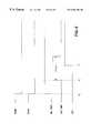
- FIG. 6is a timing diagram that shows voltage level changes of different signals with respect to each other during a program verification operation.
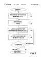
- FIG. 7is a flow diagram of a process of performing a program verification operation.
- FIG. 1is a block diagram of a flash memory device which uses a sensing time control device and method of the present invention.
- a memory cell array 1is comprised of rows and columns of memory cells. The rows of memory cells are generally referred to as word lines and the columns of memory cells are generally referred to as bit lines.
- the memory cells in the memory cell arrayare addressable with first and second x-decoders 11 and 13 and first and second y-decoders 7 and 9 .
- the memory cell arrayincludes a number of memory cell blocks, each of which contains a number of rows of memory cells.
- the first x-decoderis used to select a first group of memory cell blocks while the second x-decoder is used to select a second group of memory cell blocks.
- the first x-decoderis used to select even numbered memory cell blocks, i.e., memory cell blocks 0 , 2 , 4 , etc.
- the second x-decoderis used to selected odd numbered memory cell blocks, i.e., memory cell blocks 1 , 3 , 5 , etc.
- the first y-decoderis used to select a first group of columns of memory cells while the second y-decoder is used to select a second group of columns of memory cells.
- nis the number of columns of memory cells in a memory cell array
- the first y-decoderis used to select the first group of n/2 columns of memory cells while the second y-decoder is used to select the second group of n/2 columns of memory cells.
- the first and second x-decoders and the first and second y-decodersreceive memory addresses from an address register 21 .
- the memory addressesare decoded by the first and second x-decoders to select rows of memory cells for read, program, erase and verification operations.
- the memory addressesare also decoded by the first and second y-decoders to select columns of memory cells for read, program, erase and verification operations.
- a high voltage circuit 17provides voltages to the first and second x-decoders 11 and 13 to apply to selected memory cells. Different levels of voltages are provided to the memory cells for different operations. The levels of voltages which should be provided to the memory cells during different operations are well known in the art.
- first and second data register and sense amplifier circuits 3 , 5interface, respectively, with first and second groups of columns of memory cells.
- the first and second data register and sense amplifier circuitsread and store data from selected memory cells.
- the datais transferred from the first and second data register and sense amplifier circuits to an I/O register and buffer 15 to be transferred out of the flash memory device.
- the first and second data register and sense amplifier circuitsreceive data to be written to selected memory cells from the I/O register and buffer 15 .
- a state machine circuit 19supplies control signals to the data register and sense amplifier circuits 3 and 5 .
- the state machine circuitcontrols the timing of signals which are used during the program verification and the erase verification operations.
- FIG. 2is a block diagram of a memory cell array 33 having 4096 columns of memory cells, and a representation of a data register and sense amplifier circuit 31 containing page buffers.
- Each column of memory cellsis associated with a corresponding bit line. Each bit line is coupled to a corresponding page buffer.
- the memory cell array 33also includes a column of reference memory cells.
- the column of reference memory cellsis associated with a reference bit line, which is coupled to a reference page buffer 35 d .
- the memory cell array 33may further include additional columns of memory cells.
- the data register and sense amplifier circuit 31may further include additional page buffers that are associated with the additional columns of memory cells.
- the first data register and sense amplifier circuit 3includes page buffers associated with the first group of 2048 columns of memory cells
- the second data register and sense amplifier circuit 5includes page buffers associated with the second group of 2048 columns of memory cells.
- the data register and sense amplifier circuit 31represents a combination of both the first and the second data register and sense amplifier circuits 3 and 5 .
- the data register and sense amplifier circuit 31 of FIG. 2includes all 4096 page buffers, each page buffer being associated with one of the 4096 columns of memory cells, from both the first and the second data register and sense amplifier circuits.
- each memory cell stringincludes sixteen memory cells, a first select gate transistor and a second select gate transistor. In each memory cell string, the memory cells and the first and second select gate transistors are coupled in series.
- the first and second select gate transistorsare at the beginning and the end of each memory cell string.
- the first select gate transistorreceives a first select gate signal SG 1 , and turns on upon assertion of the first select gate signal SG 1 .
- the first select gate transistor of a particular memory cell stringis turned on, that particular memory cell string is selected for communications with the associated page buffer.
- the second select gate transistorreceives a second select gate signal SG 2 and turns on upon assertion of the second select gate signal SG 2 .
- a source of the second select gate transistoris coupled to a Vss voltage.
- the memory cell array 33includes 4096 bit lines and a reference bit line. A drain of each of the first select gate transistors is coupled to the bit line associated with the memory cell string that includes the first select gate transistor.
- the memory cell strings 37 a-crepresent a first memory cell block comprised of 4096 adjacent memory cell strings. Since there are 1024 memory cell blocks in the flash memory device of the present invention, the memory cell strings 39 a-c represent a 1024th memory cell block comprised of 4096 adjacent memory cell strings. Thus, each of the 4096 adjacent memory cell strings in each memory cell block is coupled to the associated one of the 4096 bit lines.
- a row of memory cells, which is associated with a word line,may be read or programmed at the same time.
- the row of memory cells that is associated with a word lineis also called a page.
- the first and second x-decodersselect each memory cell block by providing the select gate signals SG 1 and SG 2 , which are applied at the first and second select gate transistors, respectively. Further, the first and second x-decoders select each page in the selected memory cell block by providing appropriate voltages at word lines 1 through 16 , each word line being associated with a page. The first x-decoder selects even memory cell block 0 , 2 , 4 . . . 1022 . The second x-decoder selects odd memory cell blocks 1 , 3 , 5 . . . 1023 .
- the first and second y-decodersselect columns, each of which includes 1024 memory cell strings which are coupled together on a bit line.
- the first y-decoderselects bit lines 0 - 255 , 512 - 767 , 1024 - 1279 , 1536 - 1791 , 2048 - 2303 , 2560 - 2815 , 3072 - 3327 and 3584 - 3839 .
- the second y-decoderselects bit line 256 - 511 , 768 - 1023 , 1280 - 1535 , 1792 - 2047 , 2304 - 2559 , 2816 - 3071 , 3328 - 3583 and 3840 - 4095 .
- the data register and sense amplifier circuit 31receives a program signal PGM, a bit line control signal BL_CTRL, a set initiation signal SET_INIT and a bias signal BIAS from the state machine circuit (shown in FIG. 1 ). These control signals are provided by the state machine circuit, and are used by the page buffers and the reference page buffer during read, program and verification operations.
- the reference page buffer 35 dreceives the set initiation signal SET_INIT from the state machine circuit and provides a set signal to each of the page buffers 35 a-c.
- FIG. 3is a block diagram illustrating an interface between an i th page buffer 32 and the reference page buffer 34 .
- Both the i th page buffer and the reference page bufferreceive the program signal PGM, the bit line control signal BL_CTRL and the bias signal BIAS.
- the reference page bufferalso receives the set initiation signal SET_INIT.
- the reference page buffergenerates a set signal SET which is provided to the i th page buffer.
- the i th page buffer and the reference page bufferare coupled to an i th bit line and the reference bit line, respectively.
- the i th page bufferserves as an interface between the i th bit line and the I/O register and buffer over the data I/O interface.
- the reference page bufferserves as an interface between the reference bit line and the I/O register and buffer over the reference data I/O interface.
- FIG. 4is a page buffer associated with an i th bit line BL i.
- a drain of a bias transistor 41is coupled to Vcc.
- a gate of the bias transistor 41is coupled to the bias signal BIAS.
- a source of the bias transistoris coupled to the i th bit line BL i. Accordingly, the bias signal BIAS controls a magnitude of a current flowing through the i th bit line BL i. If the bias signal BIAS is not asserted, approximately no current flows through the i th bit line BL i since the bias transistor is then turned off and approximately no current will flow through the bias transistor regardless of the programming status of a selected memory cell.
- the bias signal BIASis set low when it is asserted since the bias transistor 41 is a p-type transistor.
- Each bit line of a NAND type flash memory deviceis generally coupled to a bit line control transistor which is located between the bit line and an associated page buffer.
- a bit line control transistor coupled to a particular bit lineis turned on for the read and program operations of memory cells on the particular bit line. Otherwise, if the bit line control transistor is turned off, the associated page buffer is generally unable to perform the read operation or the program operation.
- a bit line control transistor 53is located between the i th bit line BL i and the page buffer with a source of the bit line control transistor 53 coupled to the i th bit line BL i and a drain of the bit line control transistor 53 coupled to the source of the bias transistor 41 .
- the bit line control transistor 53controls whether the i th bit line BL i is allowed to conduct current.
- the bit line control signal BL_CTRLis asserted to turn on the bit line control transistor 53 .
- the coupling of the source of the bias transistor 41 and the drain of the bit line control transistor 53form a node A.
- a data I/O lineis coupled to node A via a program transistor 43 .
- a source of the program transistor 43is coupled to the source of the bias transistor 41 at the node A and a drain of the program transistor 43 is coupled to the data I/O line.
- the program signal PGMis provided to a gate of the program transistor 43 .
- the program signal PGMis asserted and turns on the program transistor 43 .
- the program signal PGMgoes high when it is asserted.
- appropriate voltages applied to a selected row of memory cells, i.e., a pagedata from the I/O register and buffer over a data I/O line is applied to the i th bit line BL i through the program transistor 43 and the control transistor 53 and written to the selected memory cell of the i th bit line BL i on the selected page.
- the appropriate voltages that should be applied to the memory cells during program operationsare well known in the art.
- the program operationis completed, the data that is written is verified to enhance reliability during a program verification operation.
- the program signal PGMis not asserted. In the described embodiment, the program signal PGM stays low when it is not asserted.
- a set transistor 51 , a threshold transistor 49 and inverters 45 , 47are used during the program verification operation and the erase verification operation to check whether programming or erasing, respectively, has been performed satisfactorily.
- a source of the set transistor 51is coupled to a Vss voltage and a gate of the set transistor receives the set signal SET.
- the set signal SETWhen the set signal SET is asserted, the set transistor 51 is turned on and the Vss voltage is applied to a source of the threshold transistor 49 which is coupled to a drain of the set transistor 51 .
- the set signal SETstays high when it is asserted.
- a drain of the threshold transistor 49which forms a node B, is coupled to an input of the inverter 47 and an output of the inverter 45 .
- An output of the inverter 47is coupled to an input of the inverter 45 .
- the inverters 45 and 47form a latch.
- the latchPrior to the program verification operation or the erase verification operation, the latch is preset to a logic high at node B by applying a logic high preset voltage PRESET.
- the data I/O linehas an output of a logic low.
- the data I/O lineis coupled to an inverter (not shown), and therefore, the data received by the I/O register and buffer is a logic high when node B is at a logic high.
- non-inverted datais provided to the I/O register and buffer.
- the particular memory cellis not programmed, i.e., the particular memory cell contains a logic high.
- node B of the page bufferbecomes a logic high when the page buffer reads the particular memory cell.
- an output of a latch coupled at an input to node Bbecomes a logic low.
- the inverteris provided, therefore, at the output of the latch to re-invert the inverted data from the particular memory cell.
- the non-inverted data from the particular memory cellis provided to the I/O register and buffer.
- Both the bias transistor 41 and the bit line control transistor 53are turned on during the program and erase verification operations. If a selected memory cell during the program verification operation does not contain any charge, i.e., the memory cell is erased or not programmed, a current flows through the i th bit line BL i. Similarly during the erase verification operation, if all the memory cells of a selected memory cell block on the i th bit line BL i have been erased successfully, i.e., discharged of electrons, a current flows through the i th bit line BL i.
- a threshold voltage node A between the source of the bias transistor 41 and the drain of the bit line control transistor 53is pulled low since there is a voltage drop across the bias transistor 41 .
- the voltage at the threshold voltage node Awill be insufficient to turn on the threshold transistor 49 .
- the threshold transistor 49is not turned on, the Vss voltage from the set transistor 51 is not applied at node B. Therefore during the program verification operation, when the selected memory cell has not been programmed, a content of the latch at node B remains the same and the data I/O line provides a logic high to the I/O register and buffer through an inverter (not shown).
- the erase verification operationwhen all the memory cells of a bit line in a memory cell block have been erased, the data I/O line provides a logic high to the I/O register and buffer through an inverter (not shown).
- the threshold voltage node A between the source of the bias transistor 41 and the drain of the bit line control transistor 53is pulled high since there is no voltage drop across the bias transistor 41 .
- the voltage at the threshold voltage node Awill be sufficient to turn on the threshold transistor 49 .
- the threshold transistor 49is turned on, the Vss voltage from the set transistor 51 is applied at node B. Therefore, when the selected memory cell has been programmed, the content of the latch at node B changes to a logic low and the data I/O line provides a logic low to the I/O register and buffer through the inverter (not shown).
- the voltage at the threshold node Areaches a threshold voltage level that is enough to turn on the threshold transistor 49 .
- the sufficient time required for the threshold node A to reach the threshold voltage levelis dependent on such factors as temperature and a relative position of the selected memory cell within the memory cell array.
- the set signal SETis asserted when a pre-programmed memory cell which is positioned similarly to the selected memory cell is accurately measured.
- the set signal SETis provided to the set transistor 51 after a sufficient time is allowed for an accurate measurement of the pre-programmed memory cell which is similarly positioned as the selected memory cell.
- the set signal SETis provided by a reference page buffer associated with a reference bit line REF BL.
- the reference page bufferis shown in FIG. 5.
- a structure of the reference page bufferis similar to a structure of the page buffer associated with the i th bit line BL i.
- the reference page bufferincludes a bias transistor 61 , a program transistor 63 , inverters 65 , 67 , a threshold transistor 69 , a set initiation transistor 71 and the bit line control transistor 73 .
- the set initiation transistor 71receives a set initiation signal SET_INIT from the state machine circuit (shown in FIG. 1 ).
- the set initiation signal SET_INITis generated by the state machine circuit and provided to the set initiation transistor shortly after the end of the program operation.
- the state machine circuitgenerates the set initiation signal SET_INIT when a program operation is completed and a program voltage applied at a word line is reduced to a program verification voltage.
- the latch including inverters 65 and 67is preset to a logic high using a preset signal PRESET at node B between an output of the inverter 65 and a drain of the threshold transistor 69 .
- the set signal SETtherefore, is preset to a logic low since the logic high voltage at node B is inverted by the inverter 67 before being provided as the set signal SET.
- a reference memory cell at the word line on the reference bit lineis pre-programmed to a logic low, i.e., the floating gate of the reference memory cell has been negatively charged with electrons.
- a voltage level at the threshold voltage node A between a source of a bias transistor 61 and a drain of a bit line control transistor 73will reflect the condition of a programmed memory cell. In other words, since a floating gate of the reference memory cell has been negatively charged, no current will flow on the reference bit line.
- a threshold transistor 69receives a voltage at the gate that is sufficient to turn on the threshold transistor 69 .
- the Vss voltageis applied at node B and the output of the inverter 67 will be a logic high.
- This output of the inverter 67is the set signal SET which is provided to the set transistor 51 (shown in FIG. 4) to initiate program or erase verification operation.
- the timing of program verification operation or erase verification operationis controlled by the set initiation signal provided to the reference page buffer, and more importantly, by a programmed reference memory cell sensing time of the reference page buffer.
- FIG. 6is a timing diagram which shows relative timing of voltage transitions between different signals used during a program verification operation.
- the program signal PGMstays at a logic high.
- the state machine circuitlowers the level of the program signal to a logic low. With the logic low being applied at the gate of the program transistor, the voltage level at the threshold voltage node A is dependent upon statuses of the bias signal BIAS, the bit line control signal BL_CTRL and the floating gate of the memory cell on the bit line of the selected word line.
- the bias signal BIASWhen the program signal PGM goes to a logic low at time t a , the bias signal BIAS reaches a logic low as well. Since the bias transistor of a page buffer is a p-type transistor, the logic low bias signal BIAS applied at the gate of the bias transistor turns on the bias transistor, making it ready for a current to flow through. If no current flows through the bias transistor when it is turned on, voltage at the source of the bias transistor, and therefore the threshold voltage node A, approaches the level of voltage Vcc applied at the gate of the bias transistor. However, when current flows through the bias transistor, a voltage drop across it prevents the voltage at the threshold voltage node A from approaching Vcc.
- bit line control signal BL_CTRLgoes high and turns on the bit line control transistor. If the respective memory cell has been programmed, no current flows through the bit line and the voltage level at the threshold voltage node A approaches Vcc. If the respective memory cell has not been programmed, a current flows through the bit line and the voltage level at the threshold voltage node A does not approach Vcc.
- Both the bias signal BIAS and the bit line control signal BL_CTRLare applied at both the data bit lines and the reference bit line substantially simultaneously. Therefore, the threshold voltage at the threshold voltage node A for both the data bit lines and the reference bit line would be adjusted at the same time.
- the set initiation signal SET_INITis applied at the set transistor of the reference page buffer at time t b .
- the set initiation signal SET_INITis a pulse of about 1.0 ⁇ s in duration as shown in FIG. 6 . With the pulse held high, once the threshold voltage at the threshold voltage node A reaches a sufficient level to turn on the threshold transistor of the reference page buffer, the set signal SET is generated by the reference page buffer at time t c .
- the threshold voltage at the threshold voltage node Awill be reached and the data I/O line associated with the page buffer will be switched to a logic high. If, however, the corresponding memory cell has not been programmed, the threshold transistor does not turn on and the latches will remain at the preset value where it has been preset to a logic high at node B, and therefore a logic low at the data I/O line.
- the content of a respective memory cellis stored in the latch including the inverters 45 and 47 .
- the content of the latch at the node B (shown in FIG. 4) in each page bufferis then compared with the data in the I/O register and buffer. If the contents of the latches in the data register and sense amplifier circuit match the contents of the I/O register and buffer, the program operation has been completed successfully and no further programming is needed. Otherwise, the page that failed to pass the program verification operation is re-programmed.
- FIG. 7is a flow diagram of a process of programming and verifying a page of memory cells.
- the process in step 81programs a reference memory cell to a charged status.
- the process in step 83programs a page during one program operation.
- the process in step 85latches a content of the reference memory cell programmed in step 81 and outputs the content as the set signal.
- the set signal generated in step 85is used by the process in step 87 to latch the contents of the memory cells in the page programmed in step 83 .
- step 89compares the contents of the latches of the page buffers against corresponding data stored in the I/O register and buffer for verification of programming. If the contents of the page buffers match the corresponding data, the process returns. If the content of any page buffer does not match the corresponding data, the process once again performs the program operation of the page of step 83 and the steps for program verification.
- the present inventionprovides a sensing time control device and method for reducing data sensing latency and improving data sensing reliability.
Landscapes
- Read Only Memory (AREA)
Abstract
Description
Claims (36)
Priority Applications (6)
| Application Number | Priority Date | Filing Date | Title |
|---|---|---|---|
| US09/468,422US6304486B1 (en) | 1999-12-20 | 1999-12-20 | Sensing time control device and method |
| KR1020000041281AKR100609669B1 (en) | 1999-12-20 | 2000-07-19 | Sensing time control device and method |
| DE10037037ADE10037037B4 (en) | 1999-12-20 | 2000-07-27 | Acquisition time control device and method |
| JP2000339076AJP2001176276A (en) | 1999-12-20 | 2000-11-07 | Method for performing program verification operation, method for performing erase verification operation, detection time control circuit, and flash memory device |
| TW089127227ATW499679B (en) | 1999-12-20 | 2000-12-30 | Sensing time control device and method |
| JP2009109864AJP2009170098A (en) | 1999-12-20 | 2009-04-28 | Method for performing program verify operation, method for performing erase verify operation, and detection time control circuit |
Applications Claiming Priority (1)
| Application Number | Priority Date | Filing Date | Title |
|---|---|---|---|
| US09/468,422US6304486B1 (en) | 1999-12-20 | 1999-12-20 | Sensing time control device and method |
Publications (1)
| Publication Number | Publication Date |
|---|---|
| US6304486B1true US6304486B1 (en) | 2001-10-16 |
Family
ID=23859752
Family Applications (1)
| Application Number | Title | Priority Date | Filing Date |
|---|---|---|---|
| US09/468,422Expired - LifetimeUS6304486B1 (en) | 1999-12-20 | 1999-12-20 | Sensing time control device and method |
Country Status (5)
| Country | Link |
|---|---|
| US (1) | US6304486B1 (en) |
| JP (2) | JP2001176276A (en) |
| KR (1) | KR100609669B1 (en) |
| DE (1) | DE10037037B4 (en) |
| TW (1) | TW499679B (en) |
Cited By (92)
| Publication number | Priority date | Publication date | Assignee | Title |
|---|---|---|---|---|
| US20030151955A1 (en)* | 2000-03-10 | 2003-08-14 | Kabushiki Kaisha Toshiba | Semiconductor memory device including page latch circuit |
| US6621741B2 (en)* | 2002-01-30 | 2003-09-16 | Fujitsu Limited | System for programming verification |
| US20030210576A1 (en)* | 2002-05-13 | 2003-11-13 | Sang-Won Hwang | Programmable memory devices with latching buffer circuit and methods for operating the same |
| US6735114B1 (en)* | 2003-02-04 | 2004-05-11 | Advanced Micro Devices, Inc. | Method of improving dynamic reference tracking for flash memory unit |
| US20040218438A1 (en)* | 2003-04-30 | 2004-11-04 | Chang-Ho Do | Memory device with test mode for controlling of bitline sensing margin time |
| EP1335290A3 (en)* | 2002-01-29 | 2004-11-10 | Matsushita Electric Industrial Co., Ltd. | A memory device with an error correction function |
| US20060203566A1 (en)* | 2004-12-27 | 2006-09-14 | Infineon Technologies Ag | Nonvolatile memory device for storing data and method for erasing or programming the same |
| US20060218339A1 (en)* | 2003-05-20 | 2006-09-28 | Infineon Technologies Ag | Device and method for treating a state of a memory |
| US20070002624A1 (en)* | 2005-06-29 | 2007-01-04 | Hynix Semiconductor Inc. | Flash memory device for reducing error occurrence ratio in program operation and method of controlling program operation thereof |
| US20070030735A1 (en)* | 2005-07-28 | 2007-02-08 | Luca Crippa | Page buffer circuit and method for multi-level NAND programmable memories |
| EP1752989A1 (en)* | 2005-07-28 | 2007-02-14 | STMicroelectronics S.r.l. | NAND flash memory with erase verify based on shorter delay before sensing |
| US20070133304A1 (en)* | 2005-12-08 | 2007-06-14 | Elite Semiconductor Memory Technology Inc. | Method and apparatus for determining sensing timing of flash memory |
| US20070171729A1 (en)* | 2006-01-26 | 2007-07-26 | Micron Technology, Inc. | Memory block erasing in a flash memory device |
| KR100769782B1 (en) | 2006-04-20 | 2007-10-24 | 주식회사 하이닉스반도체 | Flash memory devices |
| US20080065823A1 (en)* | 2004-05-20 | 2008-03-13 | Stmicroelectronics S.R.L. | Method of transferring data in an electrically programmable memory |
| US20080181001A1 (en)* | 2007-01-24 | 2008-07-31 | Anobit Technologies | Memory device with negative thresholds |
| US20080212368A1 (en)* | 2007-01-23 | 2008-09-04 | Samsung Electronics Co., Ltd. | Data verification method and semiconductor memory |
| US20080239825A1 (en)* | 2007-03-30 | 2008-10-02 | Nec Electronics Corporation | Floating gate memory device with improved reference current generation |
| US20090141551A1 (en)* | 2007-11-29 | 2009-06-04 | Hynix Semiconductor Inc. | Method for performing erasing operation in nonvolatile memory device |
| US7593263B2 (en) | 2006-12-17 | 2009-09-22 | Anobit Technologies Ltd. | Memory device with reduced reading latency |
| US7672170B2 (en) | 2007-01-25 | 2010-03-02 | Samsung Electronics Co., Ltd | Flash memory device and program method thereof |
| US7697326B2 (en) | 2006-05-12 | 2010-04-13 | Anobit Technologies Ltd. | Reducing programming error in memory devices |
| US20100097849A1 (en)* | 2008-10-17 | 2010-04-22 | Samsung Electronics Co., Ltd. | Variable resistance memory device performing program and verification operation |
| CN101042924B (en)* | 2006-03-24 | 2010-05-12 | 晶豪科技股份有限公司 | Method and device for determining sensing time of flash memory element |
| US7773413B2 (en) | 2007-10-08 | 2010-08-10 | Anobit Technologies Ltd. | Reliable data storage in analog memory cells in the presence of temperature variations |
| US7821826B2 (en) | 2006-10-30 | 2010-10-26 | Anobit Technologies, Ltd. | Memory cell readout using successive approximation |
| US7864573B2 (en) | 2008-02-24 | 2011-01-04 | Anobit Technologies Ltd. | Programming analog memory cells for reduced variance after retention |
| US7900102B2 (en) | 2006-12-17 | 2011-03-01 | Anobit Technologies Ltd. | High-speed programming of memory devices |
| US7924613B1 (en) | 2008-08-05 | 2011-04-12 | Anobit Technologies Ltd. | Data storage in analog memory cells with protection against programming interruption |
| US7924587B2 (en) | 2008-02-21 | 2011-04-12 | Anobit Technologies Ltd. | Programming of analog memory cells using a single programming pulse per state transition |
| US7924648B2 (en) | 2006-11-28 | 2011-04-12 | Anobit Technologies Ltd. | Memory power and performance management |
| US7925936B1 (en) | 2007-07-13 | 2011-04-12 | Anobit Technologies Ltd. | Memory device with non-uniform programming levels |
| US7975192B2 (en) | 2006-10-30 | 2011-07-05 | Anobit Technologies Ltd. | Reading memory cells using multiple thresholds |
| US7995388B1 (en) | 2008-08-05 | 2011-08-09 | Anobit Technologies Ltd. | Data storage using modified voltages |
| US8001320B2 (en) | 2007-04-22 | 2011-08-16 | Anobit Technologies Ltd. | Command interface for memory devices |
| US8000141B1 (en) | 2007-10-19 | 2011-08-16 | Anobit Technologies Ltd. | Compensation for voltage drifts in analog memory cells |
| US8000135B1 (en) | 2008-09-14 | 2011-08-16 | Anobit Technologies Ltd. | Estimation of memory cell read thresholds by sampling inside programming level distribution intervals |
| US8050086B2 (en) | 2006-05-12 | 2011-11-01 | Anobit Technologies Ltd. | Distortion estimation and cancellation in memory devices |
| US8059457B2 (en) | 2008-03-18 | 2011-11-15 | Anobit Technologies Ltd. | Memory device with multiple-accuracy read commands |
| US8060806B2 (en) | 2006-08-27 | 2011-11-15 | Anobit Technologies Ltd. | Estimation of non-linear distortion in memory devices |
| US8068360B2 (en) | 2007-10-19 | 2011-11-29 | Anobit Technologies Ltd. | Reading analog memory cells using built-in multi-threshold commands |
| US8085586B2 (en) | 2007-12-27 | 2011-12-27 | Anobit Technologies Ltd. | Wear level estimation in analog memory cells |
| US20120030441A1 (en)* | 2010-07-29 | 2012-02-02 | Takahiro Yamashita | Semiconductor memory device detecting error |
| US8151166B2 (en) | 2007-01-24 | 2012-04-03 | Anobit Technologies Ltd. | Reduction of back pattern dependency effects in memory devices |
| US8151163B2 (en) | 2006-12-03 | 2012-04-03 | Anobit Technologies Ltd. | Automatic defect management in memory devices |
| US8156403B2 (en) | 2006-05-12 | 2012-04-10 | Anobit Technologies Ltd. | Combined distortion estimation and error correction coding for memory devices |
| US8156398B2 (en) | 2008-02-05 | 2012-04-10 | Anobit Technologies Ltd. | Parameter estimation based on error correction code parity check equations |
| US8169825B1 (en) | 2008-09-02 | 2012-05-01 | Anobit Technologies Ltd. | Reliable data storage in analog memory cells subjected to long retention periods |
| US8174905B2 (en) | 2007-09-19 | 2012-05-08 | Anobit Technologies Ltd. | Programming orders for reducing distortion in arrays of multi-level analog memory cells |
| US8174857B1 (en) | 2008-12-31 | 2012-05-08 | Anobit Technologies Ltd. | Efficient readout schemes for analog memory cell devices using multiple read threshold sets |
| US8209588B2 (en) | 2007-12-12 | 2012-06-26 | Anobit Technologies Ltd. | Efficient interference cancellation in analog memory cell arrays |
| US8208304B2 (en) | 2008-11-16 | 2012-06-26 | Anobit Technologies Ltd. | Storage at M bits/cell density in N bits/cell analog memory cell devices, M>N |
| US8225181B2 (en) | 2007-11-30 | 2012-07-17 | Apple Inc. | Efficient re-read operations from memory devices |
| US8228701B2 (en) | 2009-03-01 | 2012-07-24 | Apple Inc. | Selective activation of programming schemes in analog memory cell arrays |
| US8230300B2 (en) | 2008-03-07 | 2012-07-24 | Apple Inc. | Efficient readout from analog memory cells using data compression |
| US8234545B2 (en) | 2007-05-12 | 2012-07-31 | Apple Inc. | Data storage with incremental redundancy |
| US8238157B1 (en) | 2009-04-12 | 2012-08-07 | Apple Inc. | Selective re-programming of analog memory cells |
| US8239735B2 (en) | 2006-05-12 | 2012-08-07 | Apple Inc. | Memory Device with adaptive capacity |
| US8239734B1 (en) | 2008-10-15 | 2012-08-07 | Apple Inc. | Efficient data storage in storage device arrays |
| US8248831B2 (en) | 2008-12-31 | 2012-08-21 | Apple Inc. | Rejuvenation of analog memory cells |
| US8259506B1 (en) | 2009-03-25 | 2012-09-04 | Apple Inc. | Database of memory read thresholds |
| US8259497B2 (en) | 2007-08-06 | 2012-09-04 | Apple Inc. | Programming schemes for multi-level analog memory cells |
| US8261159B1 (en) | 2008-10-30 | 2012-09-04 | Apple, Inc. | Data scrambling schemes for memory devices |
| US8270246B2 (en) | 2007-11-13 | 2012-09-18 | Apple Inc. | Optimized selection of memory chips in multi-chips memory devices |
| US8369141B2 (en) | 2007-03-12 | 2013-02-05 | Apple Inc. | Adaptive estimation of memory cell read thresholds |
| US8400858B2 (en) | 2008-03-18 | 2013-03-19 | Apple Inc. | Memory device with reduced sense time readout |
| US8429493B2 (en) | 2007-05-12 | 2013-04-23 | Apple Inc. | Memory device with internal signap processing unit |
| US8456905B2 (en) | 2007-12-16 | 2013-06-04 | Apple Inc. | Efficient data storage in multi-plane memory devices |
| US8479080B1 (en) | 2009-07-12 | 2013-07-02 | Apple Inc. | Adaptive over-provisioning in memory systems |
| US8482978B1 (en) | 2008-09-14 | 2013-07-09 | Apple Inc. | Estimation of memory cell read thresholds by sampling inside programming level distribution intervals |
| US8495465B1 (en) | 2009-10-15 | 2013-07-23 | Apple Inc. | Error correction coding over multiple memory pages |
| US20130208538A1 (en)* | 2012-02-10 | 2013-08-15 | SK Hynix Inc. | Nonvolatile semiconductor memory apparatus and data sensing method thereof |
| US8527819B2 (en) | 2007-10-19 | 2013-09-03 | Apple Inc. | Data storage in analog memory cell arrays having erase failures |
| US8572423B1 (en) | 2010-06-22 | 2013-10-29 | Apple Inc. | Reducing peak current in memory systems |
| US8572311B1 (en) | 2010-01-11 | 2013-10-29 | Apple Inc. | Redundant data storage in multi-die memory systems |
| US8595591B1 (en) | 2010-07-11 | 2013-11-26 | Apple Inc. | Interference-aware assignment of programming levels in analog memory cells |
| US8645794B1 (en) | 2010-07-31 | 2014-02-04 | Apple Inc. | Data storage in analog memory cells using a non-integer number of bits per cell |
| US8677054B1 (en) | 2009-12-16 | 2014-03-18 | Apple Inc. | Memory management schemes for non-volatile memory devices |
| US8694854B1 (en) | 2010-08-17 | 2014-04-08 | Apple Inc. | Read threshold setting based on soft readout statistics |
| US8694853B1 (en) | 2010-05-04 | 2014-04-08 | Apple Inc. | Read commands for reading interfering memory cells |
| US8694814B1 (en) | 2010-01-10 | 2014-04-08 | Apple Inc. | Reuse of host hibernation storage space by memory controller |
| US8832354B2 (en) | 2009-03-25 | 2014-09-09 | Apple Inc. | Use of host system resources by memory controller |
| US8856475B1 (en) | 2010-08-01 | 2014-10-07 | Apple Inc. | Efficient selection of memory blocks for compaction |
| US20140347932A1 (en)* | 2011-08-25 | 2014-11-27 | Micron Technology, Inc. | Memory with three transistor memory cell device |
| US8924661B1 (en) | 2009-01-18 | 2014-12-30 | Apple Inc. | Memory system including a controller and processors associated with memory devices |
| US8949684B1 (en) | 2008-09-02 | 2015-02-03 | Apple Inc. | Segmented data storage |
| US9021181B1 (en) | 2010-09-27 | 2015-04-28 | Apple Inc. | Memory management for unifying memory cell conditions by using maximum time intervals |
| US9104580B1 (en) | 2010-07-27 | 2015-08-11 | Apple Inc. | Cache memory for hybrid disk drives |
| US10777287B2 (en) | 2018-06-14 | 2020-09-15 | Fujitsu Limited | Memory control apparatus, information processing apparatus, and memory control method |
| US11556416B2 (en) | 2021-05-05 | 2023-01-17 | Apple Inc. | Controlling memory readout reliability and throughput by adjusting distance between read thresholds |
| US11847342B2 (en) | 2021-07-28 | 2023-12-19 | Apple Inc. | Efficient transfer of hard data and confidence levels in reading a nonvolatile memory |
| US12040010B2 (en) | 2022-04-21 | 2024-07-16 | Sandisk Technologies Llc | IR drop compensation for sensing memory |
Families Citing this family (2)
| Publication number | Priority date | Publication date | Assignee | Title |
|---|---|---|---|---|
| JP5537366B2 (en)* | 2009-10-01 | 2014-07-02 | 株式会社半導体エネルギー研究所 | Driving method of semiconductor device |
| KR101525907B1 (en) | 2011-09-05 | 2015-06-04 | 니폰덴신뎅와 가부시키가이샤 | Nitride semiconductor structure and method of preparing the same |
Citations (3)
| Publication number | Priority date | Publication date | Assignee | Title |
|---|---|---|---|---|
| US5675537A (en)* | 1996-08-22 | 1997-10-07 | Advanced Micro Devices, Inc. | Erase method for page mode multiple bits-per-cell flash EEPROM |
| US5754475A (en)* | 1996-06-24 | 1998-05-19 | Advanced Micro Devices, Inc. | Bit line discharge method for reading a multiple bits-per-cell flash EEPROM |
| US6046934A (en)* | 1999-01-12 | 2000-04-04 | Macronix International Co., Ltd. | Method and device for multi-level programming of a memory cell |
Family Cites Families (7)
| Publication number | Priority date | Publication date | Assignee | Title |
|---|---|---|---|---|
| GB8923037D0 (en)* | 1989-10-12 | 1989-11-29 | Inmos Ltd | Timing control for a memory |
| JPH0652695A (en)* | 1992-07-31 | 1994-02-25 | Fujitsu Ltd | Semiconductor storage device |
| JPH06176568A (en)* | 1992-12-07 | 1994-06-24 | Fujitsu Ltd | Semiconductor memory |
| JPH08190796A (en)* | 1995-01-09 | 1996-07-23 | Mitsubishi Denki Semiconductor Software Kk | Flash memory having data refresh function and data refresh method for flash memory |
| JP3542225B2 (en)* | 1996-03-19 | 2004-07-14 | 株式会社日立製作所 | Semiconductor device |
| JPH09320286A (en)* | 1996-05-24 | 1997-12-12 | Nec Corp | Semiconductor memory |
| KR100255957B1 (en)* | 1997-07-29 | 2000-05-01 | 윤종용 | Semiconductor memory device with electrically erasable and programmable memory cells |
- 1999
- 1999-12-20USUS09/468,422patent/US6304486B1/ennot_activeExpired - Lifetime
- 2000
- 2000-07-19KRKR1020000041281Apatent/KR100609669B1/ennot_activeExpired - Lifetime
- 2000-07-27DEDE10037037Apatent/DE10037037B4/ennot_activeExpired - Fee Related
- 2000-11-07JPJP2000339076Apatent/JP2001176276A/enactivePending
- 2000-12-30TWTW089127227Apatent/TW499679B/ennot_activeIP Right Cessation
- 2009
- 2009-04-28JPJP2009109864Apatent/JP2009170098A/enactivePending
Patent Citations (3)
| Publication number | Priority date | Publication date | Assignee | Title |
|---|---|---|---|---|
| US5754475A (en)* | 1996-06-24 | 1998-05-19 | Advanced Micro Devices, Inc. | Bit line discharge method for reading a multiple bits-per-cell flash EEPROM |
| US5675537A (en)* | 1996-08-22 | 1997-10-07 | Advanced Micro Devices, Inc. | Erase method for page mode multiple bits-per-cell flash EEPROM |
| US6046934A (en)* | 1999-01-12 | 2000-04-04 | Macronix International Co., Ltd. | Method and device for multi-level programming of a memory cell |
Cited By (133)
| Publication number | Priority date | Publication date | Assignee | Title |
|---|---|---|---|---|
| US6999353B2 (en) | 2000-03-10 | 2006-02-14 | Kabushiki Kaisha Toshiba | Semiconductor memory device including page latch circuit |
| US20050052930A1 (en)* | 2000-03-10 | 2005-03-10 | Kabushiki Kaisha Toshiba | Semiconductor memory device including page latch circuit |
| US20030151955A1 (en)* | 2000-03-10 | 2003-08-14 | Kabushiki Kaisha Toshiba | Semiconductor memory device including page latch circuit |
| US6731538B2 (en)* | 2000-03-10 | 2004-05-04 | Kabushiki Kaisha Toshiba | Semiconductor memory device including page latch circuit |
| US6826116B2 (en) | 2000-03-10 | 2004-11-30 | Kabushiki Kaisha Toshiba | Semiconductor memory device including page latch circuit |
| US20040141375A1 (en)* | 2000-03-10 | 2004-07-22 | Kabushiki Kaisha Toshiba | Semiconductor memory device including page latch circuit |
| EP1335290A3 (en)* | 2002-01-29 | 2004-11-10 | Matsushita Electric Industrial Co., Ltd. | A memory device with an error correction function |
| US6621741B2 (en)* | 2002-01-30 | 2003-09-16 | Fujitsu Limited | System for programming verification |
| US6826082B2 (en)* | 2002-05-13 | 2004-11-30 | Samsung Electronics Co., Ltd. | Programmable memory devices with latching buffer circuit and methods for operating the same |
| US20030210576A1 (en)* | 2002-05-13 | 2003-11-13 | Sang-Won Hwang | Programmable memory devices with latching buffer circuit and methods for operating the same |
| US6735114B1 (en)* | 2003-02-04 | 2004-05-11 | Advanced Micro Devices, Inc. | Method of improving dynamic reference tracking for flash memory unit |
| US20040218438A1 (en)* | 2003-04-30 | 2004-11-04 | Chang-Ho Do | Memory device with test mode for controlling of bitline sensing margin time |
| US6980476B2 (en) | 2003-04-30 | 2005-12-27 | Hynix Semiconductor Inc | Memory device with test mode for controlling of bitline sensing margin time |
| CN100409362C (en)* | 2003-04-30 | 2008-08-06 | 海力士半导体有限公司 | Memory device with test mode for controlling of bitline sensing margin time |
| US20060218339A1 (en)* | 2003-05-20 | 2006-09-28 | Infineon Technologies Ag | Device and method for treating a state of a memory |
| US7328302B2 (en) | 2003-05-20 | 2008-02-05 | Infineon Technologies Ag | Device and method for treating a state of a memory |
| US7471576B2 (en)* | 2004-05-20 | 2008-12-30 | Osama Khouri | Method of transferring data in an electrically programmable memory |
| US20080065823A1 (en)* | 2004-05-20 | 2008-03-13 | Stmicroelectronics S.R.L. | Method of transferring data in an electrically programmable memory |
| US7274595B2 (en)* | 2004-12-27 | 2007-09-25 | Infineon Technologies Ag | Nonvolatile memory device for storing data and method for erasing or programming the same |
| US20060203566A1 (en)* | 2004-12-27 | 2006-09-14 | Infineon Technologies Ag | Nonvolatile memory device for storing data and method for erasing or programming the same |
| US7885113B2 (en) | 2005-06-29 | 2011-02-08 | Hynix Semiconductor Inc | Method of controlling a program control of a flash memory device |
| US20070002624A1 (en)* | 2005-06-29 | 2007-01-04 | Hynix Semiconductor Inc. | Flash memory device for reducing error occurrence ratio in program operation and method of controlling program operation thereof |
| US20090285025A1 (en)* | 2005-06-29 | 2009-11-19 | Hynix Semiconductor Inc. | Method of Controlling a Program Control of a Flash Memory Device |
| US7366014B2 (en) | 2005-07-28 | 2008-04-29 | Stmicroelectronics S.R.L. | Double page programming system and method |
| US20070030732A1 (en)* | 2005-07-28 | 2007-02-08 | Rino Micheloni | Double page programming system and method |
| US20070030730A1 (en)* | 2005-07-28 | 2007-02-08 | Stmicroelectronics S.R.I. | Nand flash memory with erase verify based on shorter evaluation time |
| US7336538B2 (en) | 2005-07-28 | 2008-02-26 | Stmicroelectronics S.R.L. | Page buffer circuit and method for multi-level NAND programmable memories |
| US20070030735A1 (en)* | 2005-07-28 | 2007-02-08 | Luca Crippa | Page buffer circuit and method for multi-level NAND programmable memories |
| US7362616B2 (en) | 2005-07-28 | 2008-04-22 | Stmicroelectronics S.R.L. | NAND flash memory with erase verify based on shorter evaluation time |
| EP1752989A1 (en)* | 2005-07-28 | 2007-02-14 | STMicroelectronics S.r.l. | NAND flash memory with erase verify based on shorter delay before sensing |
| US7263004B2 (en) | 2005-12-08 | 2007-08-28 | Elite Semiconductor Memory Technology Inc. | Method and apparatus for determining sensing timing of flash memory |
| US20070133304A1 (en)* | 2005-12-08 | 2007-06-14 | Elite Semiconductor Memory Technology Inc. | Method and apparatus for determining sensing timing of flash memory |
| US7263006B2 (en) | 2006-01-26 | 2007-08-28 | Micron Technology, Inc. | Memory block erasing in a flash memory device |
| US20070171729A1 (en)* | 2006-01-26 | 2007-07-26 | Micron Technology, Inc. | Memory block erasing in a flash memory device |
| CN101042924B (en)* | 2006-03-24 | 2010-05-12 | 晶豪科技股份有限公司 | Method and device for determining sensing time of flash memory element |
| KR100769782B1 (en) | 2006-04-20 | 2007-10-24 | 주식회사 하이닉스반도체 | Flash memory devices |
| US7564724B2 (en) | 2006-04-20 | 2009-07-21 | Hynix Semiconductor Inc. | Flash memory device |
| US20070247928A1 (en)* | 2006-04-20 | 2007-10-25 | Hynix Semiconductor Inc. | Flash memory device |
| US8599611B2 (en) | 2006-05-12 | 2013-12-03 | Apple Inc. | Distortion estimation and cancellation in memory devices |
| US8570804B2 (en) | 2006-05-12 | 2013-10-29 | Apple Inc. | Distortion estimation and cancellation in memory devices |
| US8239735B2 (en) | 2006-05-12 | 2012-08-07 | Apple Inc. | Memory Device with adaptive capacity |
| US8050086B2 (en) | 2006-05-12 | 2011-11-01 | Anobit Technologies Ltd. | Distortion estimation and cancellation in memory devices |
| US8156403B2 (en) | 2006-05-12 | 2012-04-10 | Anobit Technologies Ltd. | Combined distortion estimation and error correction coding for memory devices |
| US7697326B2 (en) | 2006-05-12 | 2010-04-13 | Anobit Technologies Ltd. | Reducing programming error in memory devices |
| US8060806B2 (en) | 2006-08-27 | 2011-11-15 | Anobit Technologies Ltd. | Estimation of non-linear distortion in memory devices |
| US8145984B2 (en) | 2006-10-30 | 2012-03-27 | Anobit Technologies Ltd. | Reading memory cells using multiple thresholds |
| US7975192B2 (en) | 2006-10-30 | 2011-07-05 | Anobit Technologies Ltd. | Reading memory cells using multiple thresholds |
| US7821826B2 (en) | 2006-10-30 | 2010-10-26 | Anobit Technologies, Ltd. | Memory cell readout using successive approximation |
| USRE46346E1 (en) | 2006-10-30 | 2017-03-21 | Apple Inc. | Reading memory cells using multiple thresholds |
| US7924648B2 (en) | 2006-11-28 | 2011-04-12 | Anobit Technologies Ltd. | Memory power and performance management |
| US8151163B2 (en) | 2006-12-03 | 2012-04-03 | Anobit Technologies Ltd. | Automatic defect management in memory devices |
| US7593263B2 (en) | 2006-12-17 | 2009-09-22 | Anobit Technologies Ltd. | Memory device with reduced reading latency |
| US7900102B2 (en) | 2006-12-17 | 2011-03-01 | Anobit Technologies Ltd. | High-speed programming of memory devices |
| US20080212368A1 (en)* | 2007-01-23 | 2008-09-04 | Samsung Electronics Co., Ltd. | Data verification method and semiconductor memory |
| US7768827B2 (en)* | 2007-01-23 | 2010-08-03 | Samsung Electronics Co., Ltd. | Data verification method and semiconductor memory |
| US7751240B2 (en) | 2007-01-24 | 2010-07-06 | Anobit Technologies Ltd. | Memory device with negative thresholds |
| US8151166B2 (en) | 2007-01-24 | 2012-04-03 | Anobit Technologies Ltd. | Reduction of back pattern dependency effects in memory devices |
| US20080181001A1 (en)* | 2007-01-24 | 2008-07-31 | Anobit Technologies | Memory device with negative thresholds |
| US7881107B2 (en) | 2007-01-24 | 2011-02-01 | Anobit Technologies Ltd. | Memory device with negative thresholds |
| US7672170B2 (en) | 2007-01-25 | 2010-03-02 | Samsung Electronics Co., Ltd | Flash memory device and program method thereof |
| US8369141B2 (en) | 2007-03-12 | 2013-02-05 | Apple Inc. | Adaptive estimation of memory cell read thresholds |
| US20080239825A1 (en)* | 2007-03-30 | 2008-10-02 | Nec Electronics Corporation | Floating gate memory device with improved reference current generation |
| US7599221B2 (en)* | 2007-03-30 | 2009-10-06 | Nec Electronics Corporation | Floating gate memory device with improved reference current generation |
| US8001320B2 (en) | 2007-04-22 | 2011-08-16 | Anobit Technologies Ltd. | Command interface for memory devices |
| US8234545B2 (en) | 2007-05-12 | 2012-07-31 | Apple Inc. | Data storage with incremental redundancy |
| US8429493B2 (en) | 2007-05-12 | 2013-04-23 | Apple Inc. | Memory device with internal signap processing unit |
| US7925936B1 (en) | 2007-07-13 | 2011-04-12 | Anobit Technologies Ltd. | Memory device with non-uniform programming levels |
| US8259497B2 (en) | 2007-08-06 | 2012-09-04 | Apple Inc. | Programming schemes for multi-level analog memory cells |
| US8174905B2 (en) | 2007-09-19 | 2012-05-08 | Anobit Technologies Ltd. | Programming orders for reducing distortion in arrays of multi-level analog memory cells |
| US7773413B2 (en) | 2007-10-08 | 2010-08-10 | Anobit Technologies Ltd. | Reliable data storage in analog memory cells in the presence of temperature variations |
| US8068360B2 (en) | 2007-10-19 | 2011-11-29 | Anobit Technologies Ltd. | Reading analog memory cells using built-in multi-threshold commands |
| US8527819B2 (en) | 2007-10-19 | 2013-09-03 | Apple Inc. | Data storage in analog memory cell arrays having erase failures |
| US8000141B1 (en) | 2007-10-19 | 2011-08-16 | Anobit Technologies Ltd. | Compensation for voltage drifts in analog memory cells |
| US8270246B2 (en) | 2007-11-13 | 2012-09-18 | Apple Inc. | Optimized selection of memory chips in multi-chips memory devices |
| US20090141551A1 (en)* | 2007-11-29 | 2009-06-04 | Hynix Semiconductor Inc. | Method for performing erasing operation in nonvolatile memory device |
| US7830717B2 (en)* | 2007-11-29 | 2010-11-09 | Hynix Semiconductor Inc. | Method for performing erasing operation in nonvolatile memory device |
| US8225181B2 (en) | 2007-11-30 | 2012-07-17 | Apple Inc. | Efficient re-read operations from memory devices |
| US8209588B2 (en) | 2007-12-12 | 2012-06-26 | Anobit Technologies Ltd. | Efficient interference cancellation in analog memory cell arrays |
| US8456905B2 (en) | 2007-12-16 | 2013-06-04 | Apple Inc. | Efficient data storage in multi-plane memory devices |
| US8085586B2 (en) | 2007-12-27 | 2011-12-27 | Anobit Technologies Ltd. | Wear level estimation in analog memory cells |
| US8156398B2 (en) | 2008-02-05 | 2012-04-10 | Anobit Technologies Ltd. | Parameter estimation based on error correction code parity check equations |
| US7924587B2 (en) | 2008-02-21 | 2011-04-12 | Anobit Technologies Ltd. | Programming of analog memory cells using a single programming pulse per state transition |
| US7864573B2 (en) | 2008-02-24 | 2011-01-04 | Anobit Technologies Ltd. | Programming analog memory cells for reduced variance after retention |
| US8230300B2 (en) | 2008-03-07 | 2012-07-24 | Apple Inc. | Efficient readout from analog memory cells using data compression |
| US8400858B2 (en) | 2008-03-18 | 2013-03-19 | Apple Inc. | Memory device with reduced sense time readout |
| US8059457B2 (en) | 2008-03-18 | 2011-11-15 | Anobit Technologies Ltd. | Memory device with multiple-accuracy read commands |
| US8498151B1 (en) | 2008-08-05 | 2013-07-30 | Apple Inc. | Data storage in analog memory cells using modified pass voltages |
| US7995388B1 (en) | 2008-08-05 | 2011-08-09 | Anobit Technologies Ltd. | Data storage using modified voltages |
| US7924613B1 (en) | 2008-08-05 | 2011-04-12 | Anobit Technologies Ltd. | Data storage in analog memory cells with protection against programming interruption |
| US8949684B1 (en) | 2008-09-02 | 2015-02-03 | Apple Inc. | Segmented data storage |
| US8169825B1 (en) | 2008-09-02 | 2012-05-01 | Anobit Technologies Ltd. | Reliable data storage in analog memory cells subjected to long retention periods |
| US8482978B1 (en) | 2008-09-14 | 2013-07-09 | Apple Inc. | Estimation of memory cell read thresholds by sampling inside programming level distribution intervals |
| US8000135B1 (en) | 2008-09-14 | 2011-08-16 | Anobit Technologies Ltd. | Estimation of memory cell read thresholds by sampling inside programming level distribution intervals |
| US8239734B1 (en) | 2008-10-15 | 2012-08-07 | Apple Inc. | Efficient data storage in storage device arrays |
| US8644061B2 (en) | 2008-10-17 | 2014-02-04 | Samsung Electronics Co., Ltd. | Variable resistance memory device performing program and verification operation |
| US20100097849A1 (en)* | 2008-10-17 | 2010-04-22 | Samsung Electronics Co., Ltd. | Variable resistance memory device performing program and verification operation |
| US8261159B1 (en) | 2008-10-30 | 2012-09-04 | Apple, Inc. | Data scrambling schemes for memory devices |
| US8208304B2 (en) | 2008-11-16 | 2012-06-26 | Anobit Technologies Ltd. | Storage at M bits/cell density in N bits/cell analog memory cell devices, M>N |
| US8248831B2 (en) | 2008-12-31 | 2012-08-21 | Apple Inc. | Rejuvenation of analog memory cells |
| US8397131B1 (en) | 2008-12-31 | 2013-03-12 | Apple Inc. | Efficient readout schemes for analog memory cell devices |
| US8174857B1 (en) | 2008-12-31 | 2012-05-08 | Anobit Technologies Ltd. | Efficient readout schemes for analog memory cell devices using multiple read threshold sets |
| US8924661B1 (en) | 2009-01-18 | 2014-12-30 | Apple Inc. | Memory system including a controller and processors associated with memory devices |
| US8228701B2 (en) | 2009-03-01 | 2012-07-24 | Apple Inc. | Selective activation of programming schemes in analog memory cell arrays |
| US8832354B2 (en) | 2009-03-25 | 2014-09-09 | Apple Inc. | Use of host system resources by memory controller |
| US8259506B1 (en) | 2009-03-25 | 2012-09-04 | Apple Inc. | Database of memory read thresholds |
| US8238157B1 (en) | 2009-04-12 | 2012-08-07 | Apple Inc. | Selective re-programming of analog memory cells |
| US8479080B1 (en) | 2009-07-12 | 2013-07-02 | Apple Inc. | Adaptive over-provisioning in memory systems |
| US8495465B1 (en) | 2009-10-15 | 2013-07-23 | Apple Inc. | Error correction coding over multiple memory pages |
| US8677054B1 (en) | 2009-12-16 | 2014-03-18 | Apple Inc. | Memory management schemes for non-volatile memory devices |
| US8694814B1 (en) | 2010-01-10 | 2014-04-08 | Apple Inc. | Reuse of host hibernation storage space by memory controller |
| US8572311B1 (en) | 2010-01-11 | 2013-10-29 | Apple Inc. | Redundant data storage in multi-die memory systems |
| US8677203B1 (en) | 2010-01-11 | 2014-03-18 | Apple Inc. | Redundant data storage schemes for multi-die memory systems |
| US8694853B1 (en) | 2010-05-04 | 2014-04-08 | Apple Inc. | Read commands for reading interfering memory cells |
| US8572423B1 (en) | 2010-06-22 | 2013-10-29 | Apple Inc. | Reducing peak current in memory systems |
| US8595591B1 (en) | 2010-07-11 | 2013-11-26 | Apple Inc. | Interference-aware assignment of programming levels in analog memory cells |
| US9104580B1 (en) | 2010-07-27 | 2015-08-11 | Apple Inc. | Cache memory for hybrid disk drives |
| US8856614B2 (en)* | 2010-07-29 | 2014-10-07 | Kabushiki Kaisha Toshiba | Semiconductor memory device detecting error |
| US20120030441A1 (en)* | 2010-07-29 | 2012-02-02 | Takahiro Yamashita | Semiconductor memory device detecting error |
| US8767459B1 (en) | 2010-07-31 | 2014-07-01 | Apple Inc. | Data storage in analog memory cells across word lines using a non-integer number of bits per cell |
| US8645794B1 (en) | 2010-07-31 | 2014-02-04 | Apple Inc. | Data storage in analog memory cells using a non-integer number of bits per cell |
| US8856475B1 (en) | 2010-08-01 | 2014-10-07 | Apple Inc. | Efficient selection of memory blocks for compaction |
| US8694854B1 (en) | 2010-08-17 | 2014-04-08 | Apple Inc. | Read threshold setting based on soft readout statistics |
| US9021181B1 (en) | 2010-09-27 | 2015-04-28 | Apple Inc. | Memory management for unifying memory cell conditions by using maximum time intervals |
| US20140347932A1 (en)* | 2011-08-25 | 2014-11-27 | Micron Technology, Inc. | Memory with three transistor memory cell device |
| US9767904B2 (en)* | 2011-08-25 | 2017-09-19 | Micron Technology, Inc. | Memory with three transistor memory cell device |
| US10014053B2 (en) | 2011-08-25 | 2018-07-03 | Micron Technology, Inc. | Methods for backup sequence using three transistor memory cell devices |
| US10141056B2 (en) | 2011-08-25 | 2018-11-27 | Micron Technology, Inc. | Memories including multiple arrays of non-volatile memory cells selectively connected to sense circuitry using different numbers of data lines |
| US9093169B2 (en)* | 2012-02-10 | 2015-07-28 | SK Hynix Inc. | Nonvolatile semiconductor memory apparatus and data sensing method thereof |
| US20130208538A1 (en)* | 2012-02-10 | 2013-08-15 | SK Hynix Inc. | Nonvolatile semiconductor memory apparatus and data sensing method thereof |
| US10777287B2 (en) | 2018-06-14 | 2020-09-15 | Fujitsu Limited | Memory control apparatus, information processing apparatus, and memory control method |
| US11556416B2 (en) | 2021-05-05 | 2023-01-17 | Apple Inc. | Controlling memory readout reliability and throughput by adjusting distance between read thresholds |
| US11847342B2 (en) | 2021-07-28 | 2023-12-19 | Apple Inc. | Efficient transfer of hard data and confidence levels in reading a nonvolatile memory |
| US12040010B2 (en) | 2022-04-21 | 2024-07-16 | Sandisk Technologies Llc | IR drop compensation for sensing memory |
Also Published As
| Publication number | Publication date |
|---|---|
| KR20010069992A (en) | 2001-07-25 |
| KR100609669B1 (en) | 2006-08-09 |
| TW499679B (en) | 2002-08-21 |
| DE10037037B4 (en) | 2008-04-03 |
| JP2009170098A (en) | 2009-07-30 |
| JP2001176276A (en) | 2001-06-29 |
| DE10037037A1 (en) | 2001-06-21 |
Similar Documents
| Publication | Publication Date | Title |
|---|---|---|
| US6304486B1 (en) | Sensing time control device and method | |
| US6031760A (en) | Semiconductor memory device and method of programming the same | |
| US7633804B2 (en) | Adjusting programming or erase voltage pulses in response to the number of programming or erase failures | |
| JP3898349B2 (en) | Semiconductor memory device | |
| US5428569A (en) | Non-volatile semiconductor memory device | |
| US5778440A (en) | Floating gate memory device and method for terminating a program load cycle upon detecting a predetermined address/data pattern | |
| US7362616B2 (en) | NAND flash memory with erase verify based on shorter evaluation time | |
| KR100471167B1 (en) | Semiconductor memory device having page buffer for verifying programmed memory device | |
| US5959882A (en) | Nonvolatile semiconductor memory device and data writing method therefor | |
| USRE44978E1 (en) | Method of verifying programming of a nonvolatile memory device | |
| US6865112B2 (en) | Non-volatile semiconductor memory device in which one page is set for a plurality of memory cell arrays | |
| USRE44350E1 (en) | Nonvolatile semiconductor memory including multi-threshold voltage memory cells including voltage ranges indicating either an erase state or a two or more program state | |
| US8605512B2 (en) | Nonvolatile semiconductor memory device and method of operating a nonvolatile memory device | |
| JPH097380A (en) | Nonvolatile semiconductor memory device | |
| US5428580A (en) | Nonvolatile semiconductor memory having an address-transition-detection circuit | |
| US7394700B2 (en) | Programming methods for a nonvolatile memory device using a Y-scan operation during a verify read operation | |
| JP3404712B2 (en) | Nonvolatile semiconductor memory device and writing method thereof | |
| JP2000048582A (en) | Semiconductor storage device | |
| US7274595B2 (en) | Nonvolatile memory device for storing data and method for erasing or programming the same | |
| KR20120005828A (en) | How Nonvolatile Memory Devices Work | |
| JPH11261034A (en) | Nonvolatile semiconductor memory device |
Legal Events
| Date | Code | Title | Description |
|---|---|---|---|
| AS | Assignment | Owner name:FUJITSU LIMITED, JAPAN Free format text:ASSIGNMENT OF ASSIGNORS INTEREST;ASSIGNOR:YANO, MASARU;REEL/FRAME:010709/0721 Effective date:20000329 | |
| STCF | Information on status: patent grant | Free format text:PATENTED CASE | |
| FEPP | Fee payment procedure | Free format text:PAYOR NUMBER ASSIGNED (ORIGINAL EVENT CODE: ASPN); ENTITY STATUS OF PATENT OWNER: LARGE ENTITY | |
| FPAY | Fee payment | Year of fee payment:4 | |
| AS | Assignment | Owner name:FUJITSU MICROELECTRONICS LIMITED, JAPAN Free format text:ASSIGNMENT OF ASSIGNORS INTEREST;ASSIGNOR:FUJITSU LIMITED;REEL/FRAME:021965/0746 Effective date:20081104 | |
| FPAY | Fee payment | Year of fee payment:8 | |
| AS | Assignment | Owner name:FUJITSU SEMICONDUCTOR LIMITED,JAPAN Free format text:CHANGE OF NAME;ASSIGNOR:FUJITSU MICROELECTRONICS LIMITED;REEL/FRAME:024597/0507 Effective date:20100401 | |
| FPAY | Fee payment | Year of fee payment:12 | |
| AS | Assignment | Owner name:SOCIONEXT INC., JAPAN Free format text:ASSIGNMENT OF ASSIGNORS INTEREST;ASSIGNOR:FUJITSU SEMICONDUCTOR LIMITED;REEL/FRAME:035508/0637 Effective date:20150302 |