US6303961B1 - Complementary semiconductor devices - Google Patents
Complementary semiconductor devicesDownload PDFInfo
- Publication number
- US6303961B1 US6303961B1US09/069,215US6921598AUS6303961B1US 6303961 B1US6303961 B1US 6303961B1US 6921598 AUS6921598 AUS 6921598AUS 6303961 B1US6303961 B1US 6303961B1
- Authority
- US
- United States
- Prior art keywords
- well
- channel
- region
- type
- major surface
- Prior art date
- Legal status (The legal status is an assumption and is not a legal conclusion. Google has not performed a legal analysis and makes no representation as to the accuracy of the status listed.)
- Expired - Lifetime
Links
Images


Classifications
- H—ELECTRICITY
- H10—SEMICONDUCTOR DEVICES; ELECTRIC SOLID-STATE DEVICES NOT OTHERWISE PROVIDED FOR
- H10D—INORGANIC ELECTRIC SEMICONDUCTOR DEVICES
- H10D30/00—Field-effect transistors [FET]
- H10D30/60—Insulated-gate field-effect transistors [IGFET]
- H10D30/64—Double-diffused metal-oxide semiconductor [DMOS] FETs
- H10D30/66—Vertical DMOS [VDMOS] FETs
- H10D30/667—Vertical DMOS [VDMOS] FETs having substrates comprising insulating layers, e.g. SOI-VDMOS transistors
- H—ELECTRICITY
- H10—SEMICONDUCTOR DEVICES; ELECTRIC SOLID-STATE DEVICES NOT OTHERWISE PROVIDED FOR
- H10D—INORGANIC ELECTRIC SEMICONDUCTOR DEVICES
- H10D10/00—Bipolar junction transistors [BJT]
- H10D10/01—Manufacture or treatment
- H10D10/041—Manufacture or treatment of thin-film BJTs
- H—ELECTRICITY
- H10—SEMICONDUCTOR DEVICES; ELECTRIC SOLID-STATE DEVICES NOT OTHERWISE PROVIDED FOR
- H10D—INORGANIC ELECTRIC SEMICONDUCTOR DEVICES
- H10D10/00—Bipolar junction transistors [BJT]
- H10D10/311—Thin-film BJTs
- H—ELECTRICITY
- H10—SEMICONDUCTOR DEVICES; ELECTRIC SOLID-STATE DEVICES NOT OTHERWISE PROVIDED FOR
- H10D—INORGANIC ELECTRIC SEMICONDUCTOR DEVICES
- H10D12/00—Bipolar devices controlled by the field effect, e.g. insulated-gate bipolar transistors [IGBT]
- H10D12/01—Manufacture or treatment
- H—ELECTRICITY
- H10—SEMICONDUCTOR DEVICES; ELECTRIC SOLID-STATE DEVICES NOT OTHERWISE PROVIDED FOR
- H10D—INORGANIC ELECTRIC SEMICONDUCTOR DEVICES
- H10D12/00—Bipolar devices controlled by the field effect, e.g. insulated-gate bipolar transistors [IGBT]
- H10D12/411—Insulated-gate bipolar transistors [IGBT]
- H10D12/421—Insulated-gate bipolar transistors [IGBT] on insulating layers or insulating substrates, e.g. thin-film IGBTs
- H—ELECTRICITY
- H10—SEMICONDUCTOR DEVICES; ELECTRIC SOLID-STATE DEVICES NOT OTHERWISE PROVIDED FOR
- H10D—INORGANIC ELECTRIC SEMICONDUCTOR DEVICES
- H10D18/00—Thyristors
- H10D18/01—Manufacture or treatment
- H10D18/031—Manufacture or treatment of lateral or planar thyristors
- H—ELECTRICITY
- H10—SEMICONDUCTOR DEVICES; ELECTRIC SOLID-STATE DEVICES NOT OTHERWISE PROVIDED FOR
- H10D—INORGANIC ELECTRIC SEMICONDUCTOR DEVICES
- H10D18/00—Thyristors
- H10D18/251—Lateral thyristors
- H—ELECTRICITY
- H10—SEMICONDUCTOR DEVICES; ELECTRIC SOLID-STATE DEVICES NOT OTHERWISE PROVIDED FOR
- H10D—INORGANIC ELECTRIC SEMICONDUCTOR DEVICES
- H10D18/00—Thyristors
- H10D18/60—Gate-turn-off devices
- H—ELECTRICITY
- H10—SEMICONDUCTOR DEVICES; ELECTRIC SOLID-STATE DEVICES NOT OTHERWISE PROVIDED FOR
- H10D—INORGANIC ELECTRIC SEMICONDUCTOR DEVICES
- H10D30/00—Field-effect transistors [FET]
- H10D30/60—Insulated-gate field-effect transistors [IGFET]
- H10D30/64—Double-diffused metal-oxide semiconductor [DMOS] FETs
- H10D30/65—Lateral DMOS [LDMOS] FETs
- H10D30/657—Lateral DMOS [LDMOS] FETs having substrates comprising insulating layers, e.g. SOI-LDMOS transistors
- H—ELECTRICITY
- H10—SEMICONDUCTOR DEVICES; ELECTRIC SOLID-STATE DEVICES NOT OTHERWISE PROVIDED FOR
- H10D—INORGANIC ELECTRIC SEMICONDUCTOR DEVICES
- H10D86/00—Integrated devices formed in or on insulating or conducting substrates, e.g. formed in silicon-on-insulator [SOI] substrates or on stainless steel or glass substrates
- H10D86/201—Integrated devices formed in or on insulating or conducting substrates, e.g. formed in silicon-on-insulator [SOI] substrates or on stainless steel or glass substrates the substrates comprising an insulating layer on a semiconductor body, e.g. SOI
Definitions
- the present inventionrelates to semiconductor devices and, more particularly, to a metal-oxide semiconductor device that has an improved compatibility for use in a CMOS device and may be integrated on a chip with a DMOS of opposite-type conductivity.
- MOSFETmetal-oxide semiconductor field effect transistor
- CMOScomplementary metal-oxide semiconductor field effect transistor
- CMOS devicesprovide significant advantages in terms of their low power consumption, but they generally require more complex processing as compared with NMOS devices. Also, with present technology, CMOS structures have been confined to low voltage devices operable at less than 5V.
- N-channel DMOS or IGBT devices operating at medium (10-100) and high (>100) voltagesmay be made to be complementary with p-channel DMOS devices, but presently this is achieved by separately fabricating the complementary p-channel devices, using different processing steps, which then may be coupled to the n-channel devices.
- CMOS devicesare not integrated simultaneously on one chip.
- FIG. 1Athere is shown a cross-sectional view of a prior art n-channel MOS device, without double diffusion.
- the characteristic features of this basic devicecomprise a p-type semiconductor substrate 12 having a major surface 14 , within which are disposed two n+ regions or bodies 16 a , 16 b , forming a source and drain, respectively.
- a gate electrode 20typically fabricated with polysilicon or a combination of polysilicon and silicide (MoSi 2 ), separated from surface 14 by a layer of gate oxide 22 .
- Field oxide layer 24isolates the source and drain, and a protective layer of glass 34 , typically boron phosphorus silicate glass, is disposed over the device.
- a further silicon nitride layermay be disposed over the glass.
- the channel 23is defined by the upper portion of the substrate 12 , which underlies gate 20 .
- FIG. 1Ashows an n-channel device (NMOS), but a p-channel device (PMOS) may be formed following the same schematic by substituting p for n and reversing the polarity of the charges.
- FIG. 1Billustrates a basic CMOS structure involving NMOS and PMOS devices integrated on the same chip, following the structure for the MOS of FIG. 1 A and using like character numerals to refer to like features.
- Metallization region 35typically fabricated with aluminum, may be deposited over the device and etched as desired (as shown), for interconnection of the device structures.
- the gate of the NMOS device 30may be connected to the gate of the PMOS device 40 .
- a conductive conduit 38having contact V G , is shown schematically with hatched lines interconnecting the gates.
- a p-tub or well 18is implanted in the n-substrate, enabling formation of the complementary devices in substrate 12 .
- p-type regionsgenerally are formed by implantation with boron ions, and n-type regions by implantation with arsenic or phosphorus ions. Because of the p-tub 18 and the processing needed to make the PMOS, the number of steps for fabricating the basic CMOS of FIG. 1B is essentially double that for the NMOS of FIG. 1 A.
- FIG. 2Athere is shown a basic embodiment of a double-diffused, n-channel MOS, again with like numerals used to refer to like features as compared with FIGS. 1A-1B.
- Substrate 12 of n-type conductivityis disposed within a chip 100 and isolated from it by a layer of dielectric material 102 , such as silicon dioxide.
- the substrate 12has a major surface 14 on which active components are disposed, e.g., gate electrode 20 insulated by gate oxide layer 22 .
- the device here showncomprises spaced-apart, plural source regions connected in parallel.
- Source regionscomprise first doped regions 17 of n-type conductivity, connected by source electrodes 21 , and second doped regions 19 of p-type conductivity formed within substrate 12 .
- a region of p+ type conductivity 25may be implanted beneath source contacts 21 , interposed between each of the doped bodies comprising the source regions, as also described in U.S. Pat. No. 5,541,429, “Dielectrically Isolated Semiconductor Devices Having Improved Characteristics,” issued Sep. 17, 1996 to M. A. Shibib, the inventor herein, assigned to AT&T Corp., a predecessor of the assignee herein, which is incorporated herein by reference.
- the second doped regions 19extend further laterally under gate electrode 20 than first doped regions 17 .
- the portions 23 of the second doped regions 19 extending beyond the first regions 17 beneath the gate oxidecomprise the channel regions of the device, and the substrate beneath the surface portion comprises a drain region.
- a doped body 26 of n+ conductivityforms a supplemental drain region in contact with drain electrode 27 .
- a heavily-doped region 28may extend laterally along the bottom of the substrate and then vertically upwardly to drain electrode 27 . This channel 28 provides a low resistance path for current to the drain electrode for controlling the current as the DMOS devices typically are used in applications involving high voltages and currents.
- the Insulated Gate Bipolar Transistorscan be identical to the DMOS devices illustrated in FIG. 2A, except that certain high conductivity regions are of opposite type conductivity to that of the substrate 12 .
- FIG. 3Ashows a prior art n-channel IGBT device, wherein doped regions 76 , 77 are of opposite conductivity to the substrate.
- CMOScomplementary to n-channel DMOS and IGBT devices
- a CMOSsuch as illustrated in FIG. 1B may be fabricated by implantation or diffusion of the doped regions in the n-type substrate.
- this CMOSwould not be self-aligned or double-diffused. This results in a less efficient device and need for a larger device to achieve the same performance parameters than if the complementary p-channel device were double-diffused.
- CMOS devicesare available for applications of up to 5 volts.
- 0 to 10 voltsis considered low voltage
- 10 to 100 voltsis considered medium voltage
- devices operating at above 100 voltsare considered high voltage devices.
- Complementary DMOS and IGBT structuresmay be built on separate chips and interconnected, but fabricating complementary p-channel structures involves processes and technologies differing from those used for the n-channel DMOS and IGBT structures.
- To make a p-channel device complementary to an n-channel DMOS devicetypically the fabrication processes are reversed on a separate chip, that is, instead of an n-type substrate, a p-type substrate is used.
- An n-well or tubmay be implanted or infused into the substrate, and p+ bodies are implanted into the n-well. While this produces a double-diffused, efficient device operating at medium or high voltage, the process is time consuming.
- CMOS technologies involving DMOS devicesbeyond the need to use separate chips and technologies, involves use of the p-type base regions.
- P-type substratesare expensive to form and often call for processing steps incompatible with standard fabrication procedures which are generally based upon n-well implantation processes.
- the inventionhas utility for better optimizing the features of various devices in integrated circuits of the type described above and in reducing the processing steps for fabricating a variety of MOS and bipolar complementary devices.
- the inventionprovides a cost-effective method of fabricating a complementary high voltage MOS and bipolar structure on the same chip and with the same substrate as a DMOS of opposite-type conductivity. Further advantages may appear more fully upon considering the description given below.
- a complementary p-channel DMOS devicemay be fabricated on the same chip as an n-channel DMOS portion by adding one step to the process of fabricating an n-channel DMOS, the step comprising the addition of an n-type body.
- a lateral p-wellis interposed between the n-type substrate of the p-channel device and the added n-type body, the lateral p-well being in contact with the drain region of the p-channel DMOS.
- one embodiment of the improved devicecomprises a substrate of a first conductivity type and first doping concentration with a major surface.
- a lateral lower well of a second conductivity typeis disposed in the substrate.
- the lower wellhas an upper boundary which is contiguous the major surface and defines a drain region.
- a first conductive region defining a gateis disposed on a portion of the major surface; the gate has a substantially vertical edge defining an opening to the major surface, and it is in contact with the lower well.
- a first upper wellis disposed in the lower well, the first upper well being of the first conductivity type and surrounded on at least a portion of the sides by the lower well.
- a channel in the first upper wellextends to the major surface and is in conductive relation with the gate.
- At least two impurity regionsare disposed in the first upper well. At least one of them is of the first conductivity type, and another is of the second conductivity type. The impurity region of the second conductivity type is in direct contact with the channel for the flow of current of the second conductivity type to the lower well.
- a second conductive regionis disposed on the major surface in contact with the at least two impurity regions.
- a second upper well of the second conductivity typealso is disposed in the lower well, defining a drain extension or supplemental drain region, and it is separated from the first upper well by the lower well.
- At least one impurity bodyis disposed in the second upper well, and a third conductive region is disposed on the major surface in contact with this impurity body.
- a complementary p-channel DMOS, IGBT, or quasi-vertical p-n-p devicecan be simultaneously integrated on the same chip as a double-diffused n-channel MOS, and vice versa.
- the inventionencompasses a doubly-diffused CMOS device for medium voltage applications.
- FIG. 1Ais a cross-sectional view of a portion of a prior art MOS device showing basic device features
- FIG. 1Bis a cross-sectional view of a prior art CMOS having PMOS and NMOS portions
- FIG. 2Ais a cross-sectional view of a prior art n-channel DMOS device
- FIG. 2Bis a cross-sectional view of an inventive p-channel DMOS device complementary to the n-channel device of FIG. 2A;
- FIG. 3Ais a cross-sectional view of a prior art n-channel IGBT device
- FIG. 3Bis a cross-sectional view of an inventive p-channel IGBT device complementary to the n-channel device of FIG. 3A;
- FIG. 4Ais a cross-sectional view of a prior art n-p-n transistor
- FIG. 4Bis a cross-sectional view of an inventive p-n-p transistor complementary to the device of FIG. 4A;
- FIGS. 5A and 5Billustrate cross-sectional views of alternate embodiments of inventive CMOS structures with the threshold voltages of the PMOS and NMOS portions matching the threshold voltages of high voltage p-channel DMOS and n-channel DMOS, respectively;
- FIGS. 6A and 6Billustrate cross-sectional views of alternate embodiments of inventive p-channel DMOS (FIG. 6A) and IGBT (FIG. 6B) devices;
- FIGS. 7A and 7Billustrate cross-sectional views of vertical (FIG. 7A) and lateral (FIG. 7 B), gate-turn-off (GTO) thyristors that may be realized following the inventive process;
- FIGS. 8A-8Nare cross-sectional views showing illustrative processing steps for making a portion of an inventive MOS device.
- a complementary p-channel DMOS devicemay be fabricated by adding one step to the fabrication process for making an n-channel DMOS, thus providing an efficient process for making a p-channel DMOS and enabling the fabrication of complementary NMOS and PMOS devices simultaneously on the same chip using the same n-type substrate.
- the discoveryinvolves use of a lateral p-well above the n-type substrate, in contact with the drain region of the device, and an additional, inventive n-body disposed in the p-well.
- This discoveryhas applicability to complementary MOS devices in general, including n- and p-channel devices referred to as DMOS, PMOS, IGBT, DGDMOS, and p-n-p transistors.
- any n-channel devicemay be formed as a p-channel device by substituting the regions of conductivity and reversing the polarity of the charges, i.e., substituting p+ for n ⁇ and vice versa.
- the specific references herein to n-channel and p-channel regionsare for purposes of illustration, as the concepts and device features specifically described herein may apply equally to devices of opposite-type conductivity.
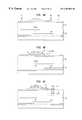
- FIG. 2Billustrates a cross-sectional view of an inventive MOS having enhanced compatibility for use in a CMOS structure.
- the inventive p-channel DMOS device of FIG. 2Bis complementary to the n-channel device of FIG. 2A, and it may be fabricated on the same substrate 12 and integrated simultaneously on the same chip 100 as the complementary n-channel DMOS (FIG. 2 A).
- the general configuration and concepts illustrated in FIG. 2Amay be applied to fabricate analogous IGBT, p-n-p transistor, CMOS, or medium voltage PMOS devices, which are illustrated in FIGS. 3-7 and described further below.
- the substrate 12is of a first conductivity type, shown as n-type, and may be isolated from the chip 100 by a layer of oxide or dielectric material 102 , with a highly-doped n+ region 28 underlying the substrate, as with the DMOS of FIG. 2 A.
- the substrate 12also has a major surface 14 on which active components are disposed.
- the lower well 60has a first depth D 1 , thus terminating above the n-substrate to form a p-n junction.
- the upper boundary 64 of the lower wellis contiguous the major surface; that is, it is aligned with the major surface and thereby defines a portion of it.
- the upper area of the lower well adjacent the boundary 64may comprise a drain region.
- a first conductive region or gate electrode 70is disposed over a portion of the major surface 14 , insulated by oxide layer 72 of dielectric material.
- An edge of the gate electrode 74defines an opening to the major surface, i.e., region O R which is not covered by gate 70 .
- a first upper well 66is disposed in the lower well 60 , and is of the first conductivity type, i.e., shown as n-type conductivity, the same conductivity type as the substrate 12 , although it may have a different concentration of dopants than the substrate. It is surrounded by the p-well 60 , or in other words, it has a depth D 2 less than the depth D 1 of the p-well 60 , with a limited width at its upper surface area, contiguous the major surface, defining its boundary.
- the lateral p-well 60may surround the bottom and sides of the first upper well 66 , as shown in FIG. 2B, or it may abut only a side portion of the upper well 66 , as shown in FIGS. 6A-6B.
- An important considerationis that the p-well 60 define a path for the flow of current of the second conductivity type (shown as p-type), from a channel 73 portion to the drain region.
- the channel portion 73is located in the first upper well adjacent and extending to the major surface 14 and disposed outside the open region OR, i.e., aligned under gate electrode 70 .
- the channel 73is in conductive relation with the gate 70 .
- a plurality of impurity regionsare disposed in the first upper well. At least one of the impurity regions (e.g., 67 a ), is of the second conductivity type (i.e., p-type), so that a p-n junction is formed in the first upper well 66 .
- Impurity region 67 ais basically aligned under the open region O R .
- the first upper well 66extends laterally under gate electrode 70 , forming channel region 73
- the lower well 60extends even further laterally traversing the width of the gate electrode 70 and in contact with the drain extension.
- the impurity region of the second conductivity type(e.g., 67 a ) is in direct contact with the channel 73 , so that current of the second conductivity type (p-type) may flow in the channel toward drain region, i.e., adjacent the upper boundary of p-well 60 , thereby defining the p-channel device.
- Each of the impurity regionshas an impurity region depth D IR less than the second depth; in other words, each is bounded on at least a portion of its bottom by upper well region 66 .
- One or more of the impurity regionsalso may be surrounded on the sides by the upper well region 66 , or preferably they may have one or more common or overlapping sides, as shown and described, for example, in U.S. Pat. No. 5,541,429 (FIG. 2 ), or U.S. Pat. No. 5,591,657 (FIG. 18 ).
- a second conductive region 71may be disposed on the major surface and in contact with the impurity regions 67 a , 67 b . In the case of the DMOS p-channel device shown in FIG. 2B, second conductive region 71 defines a source electrode.
- the conductive region 71defines a cathode, and for a p-n-p transistor (FIG. 4 B), conductive region 71 defines an emitter contact and base contact.
- At least one second upper well 76is disposed in the lower p-well 60 , with the drain region of the lower p-well (i.e., adjacent the upper boundary of the p-well) interposed between the first and second upper wells.
- the second upper well 76is of the same conductivity and polarity as the p-well, but has a different doping concentration.
- the second upper well 76has a depth less than that of the first depth, which may be the same as the second depth D 2 but need not be.
- the second upper well 76is preferably surrounded by the p-well 60 on its bottom and sides, as shown.
- the first upper wellAs with the first upper well, it has an upper surface area contiguous the major surface 64 defining its width or outer boundary. At least one doped body 77 is disposed in the second upper well (the term “doped body” being used to distinguish this impurity region from the impurity region 67 in the first upper well).
- the doped body 77is of the second conductivity type (e.g., p-type), having a different doping concentration and polarity than the second upper well 76 , defining a supplemental drain region or drain extension.
- this doped body 77may be of the first conductivity type (n-type), to form an anode region (FIG. 3 B).
- this doped body 77is of the second conductivity type to form a collector region.
- a third conductive region 81is disposed on the major surface in contact with the at least one doped body 77 , for forming a drain contact (FIG. 2 B), an anode of an IGBT (FIG. 3 B), or a collector contact of a p-n-p transistor (FIG. 4 B).
- a conductive conduit(not shown) may connect the gate of the inventive complementary p-channel DMOS device to an n-channel MOS device (e.g., FIG. 2 B).
- a layer of protective glassmay be deposited over the device which may further be covered by a passivation layer of silicon nitride (not shown).
- FIG. 3Ais a cross-sectional view of an n-channel IGBT device
- FIG. 3Ais a cross-sectional view of an n-channel IGBT device
- FIG. 3Bshows a cross-sectional view of an inventive p-channel IGBT device complementary to the device of FIG. 3 A.
- the IGBT deviceis fabricated on n-type substrate 12 , as with the DMOS of FIGS. 2A-2B and the n-channel IGBT of FIG. 3 A.
- a lateral p-well layer 60is disposed over the substrate 12 .
- First conductive region 70comprises the gate, and impurity regions 67 a , 67 b , etc. of the first upper well layer 66 are connected via second conductive region 71 to form the cathode (C).
- Doped body 79 of the second upper well region 76is of opposite-type conductivity as compared with the second upper well 76 and lower well 60 , to form the anode region, with third conductive region 81 comprising the anode (A).
- FIGS. 4A and 4Bthere are shown cross-sectional views of an n-p-n transistor and inventive complementary p-n-p transistor, respectively.
- FIG. 4Bas in FIGS. 2B and 3B, a laterally diffused p-well layer 60 is shown.
- An inventive an n-body region 66 ′is formed (the base region of the p-n-p transistor), enabling the fabrication of the complementary device in n-type substrate 12 .
- the first upper wellhas first and second impurity regions 69 a , 69 b , for forming the emitter (E) and base (B), respectively, and the doped body 77 of the second upper well 76 forms a collector (C).
- First, second, and third conductive regions 70 ′, 71 ′, 4 and 81 ′,form collector (C), emitter (E), and base (B) contacts, which typically will extend above the top surface of the chip (not shown).
- FIGS. 5A and 5Bthere are illustrated cross-sectional views of alternate embodiments of inventive CMOS structures with the threshold voltages of the NMOS (200) and PMOS (300) portions matching the threshold voltages of the high voltage p-channel DMOS and n-channel DMOS, respectively.
- first, second, and third conductive regions70 ′′, 71 ′′, and 81 ′′
- form the gate, source, and drain contactsrespectively.
- the additional n-bodye.g., 66 ′, 66 ′′
- FIGS. 6A and 6Billustrate cross-sectional views of alternate embodiments of inventive p-channel DMOS (FIG. 6A) and IGBT (FIG. 6B) devices.
- the lateral p-well 60comprises a first portion 60 a and second portion 60 b , such that a portion of the bottom W B of the first upper well 66 abuts the substrate 12 , as opposed to being surrounded by the p-well 60 , as in FIGS. 2B and 3B.
- FIGS. 7A and 7Billustrate cross-sectional views of vertical (FIG. 7A) and lateral (FIG. 7 B), gate-turn-off (GTO) thyristors that may be realized following the inventive technology, wherein the p-well 60 ′′ surrounds the anode (A) of the device.
- Lateral GTO(FIG. 7 B), has a plurality of gate contacts 70 a , 70 b , 70 c.
- the inventive technologycan be applied to various complementary MOS and bipolar CMOS structures, with FIGS. 2A-7B showing illustrative embodiments, and each of the devices may be integrated on a chip 100 having an n-type base region or substrate 12 .
- the process for fabricating the inventive MOS devicesis cost-effective, uses chip area efficiently, and involves a short process cycle as compared with prior methods of fabricating complementary p-channel and CMOS structures.
- the processcan be implemented for all BiCDMOS products and push-pull stages (both analog and high voltage).
- the CMOS structuremay be integrated on a chip having threshold voltages comparable to medium and high voltage DMOS devices.
- the inventionis particularly advantageous in that it enables fabrication of a CMOS structure basically by adding one implantation step to present technology involving fabrication of n-channel devices.
- a known fabrication sequence for making an n-channel DMOS or n-p-n transistorcan be summarized as having the following masking steps: 1) deep n+ diffusion; 2) p-well body diffusion 3) field oxide formation; 4) gate oxide formation; 5) polysilicon deposition and etch (for gate formation); 6) p ⁇ type body implantation (to form the body of a double-diffused MOS or base of an n-p-n transistor); 7) p+ body implantation (to form the source or drain of the MOS or the emitter or collector region of the n-p-n transistor); 8) p-glass or boron phosphor silicate glass (BPSG) deposition; 9) contact etch; 10) metal deposition and etch; and 11) plasma nitride deposition and etch.
- BPSGboron phosphor silicate glass
- a p-channel complementary MOS and a BiCMOS devicemay be fabricated essentially by adding one implantation step to these steps and enhancing the lateral diffusion of one region (i.e., p-well of step 2, above).
- the added implantation stepinvolves an n-type body implantation (to form the n-body of a p-channel DMOS and IGBT, the base of a vertical p-n-p transistor, the gate of a vertical GTO thyristor, and threshold control implant for p-channel devices).
- the additional implantation stepadvantageously is performed after the polysilicon deposition and etch (e.g., after step 5, above).
- FIGS. 8A-8Nshow sequential masking steps for one process of fabricating a portion of the p-channel DMOS device falling within region 8 — 8 of FIG. 2 B.
- FIGS. 8A-8Nshow one way in which an inventive MOS may be fabricated for purposes of illustration, and that only a select portion of the device is shown (i.e., region 8 — 8 , FIG. 2 B), as reflected by bending vertical sides in each of these figures. It is understood this example is not limiting in nature and that variations may be made by one skilled in the art to fabricate other inventive MOS devices and transistors.
- a dielectrically-isolated substratehas been prepared applying principles known in the field.
- the preparation stepsmay include etching with KOH solution to form v-grooves, implantation of arsenic ions throughout the nonplanar surfaces, thermally growing of approximately two microns of isolation oxide on the substrate, and growing of a relatively thick (e.g., 250 ⁇ m) layer of polycrystalline silicon over the oxide.
- the wafermay then be flipped and polished to the required thickness to provide the substrate 62 of FIG. 8A, isolated by the layer of dielectric material 102 and having a highly-doped channel region 28 .
- Other substratesmay be used as well and altered based on the device application, as is known in the field.
- the first masking stepinvolves deep n+ diffusion, generally accomplished with phosphorus or arsenic ions to place a sinker diffusion in selected areas to define regions of contact enhancement to the n-type region.
- An oxide layer(not shown), also may be formed on the device also to aid in defining the regions of contact enhancement.
- the third and fourth stepsare illustrated. They involve depositing a blanket layer of oxides 24 and a confined gate oxide layer 72 over the substrate 62 , to form the field oxide layer and gate oxide layers, having desired thicknesses.
- the oxide layerscomprise silicon dioxide, but other materials may be used as well, as are known in the field.
- thin oxide regionsdefine the active region (A R ) of the device.
- FIG. 8Eillustrates the next masking step of depositing a polysilicon layer 70 over a portion of the major surface to define a gate electrode.
- the polysiliconmay be deposited using low pressure CVD and may be doped to n+ type conductivity using one of several techniques, such as ion implantation or in situ doping with phosphorus. However, the polysilicon layer also may be undoped or doped with a p-type conductivity.
- the polysiliconmay be patterned by plasma etching through a photoresist mask, overlying oxide layers 24 , 72 . It has vertical edge 74 extending beyond gate oxide layer 72 , which is useful in defining an open area O R , a self-alignment tool in forming doped bodies within the substrate.
- the sixth masking stepcomprises implanting or diffusing n-type dopants in the p-well region 60 , using vertical edge 74 of the polysilicon layer as an alignment body (FIG. 8 F), and then laterally diffusing the dopants to form the n-body 66 (FIGS. 8 G- 8 H).
- the oxide layeris sufficiently thin that n- and p-type ions may pass through it and penetrate the major surface 64 , thereby forming underlying doped regions 66 , 76 , etc.
- the lateral diffusionmay be performed by annealing the structure at elevated temperatures, as is known to those skilled in the field.
- the p-body 76may then be formed, as illustrated with FIGS. 8G and 8H, which likewise may be accomplished by implanting p-type ions (e.g., with boron).
- the next masking stepsinvolve implantation of p-type and n-type ions (FIG. 8 I), to form the p+ and n+ impurity bodies, 67 a , 67 b , etc., and p+ doped body 77 (FIG. 8 J).
- FIG. 8Kshows impurity bodies 67 a , 67 b , separated by a portion of the upper well 66 , though preferably the bodies will be overlapping as in FIG. 2 B.
- the n+ impurity 67may be implanted before the p+ region 77 , or vice versa.
- the p-well 60may be implanted and diffused after implantation of the first upper well or n-type body 66 , so that it is interposed between the source and drain regions but does not fully underlie the first upper well 66 , as shown in FIGS. 6A-6B.
- An important considerationis that the p-well 60 be diffused or implanted laterally to be interposed between portions of the first and second upper wells 66 , 76 .
- a layer of protective glass 90(FIG. 8 J), may be deposited on the structure.
- a blanket layer of boron phosphorus silicate glassmay be deposited by LPCVD over the exposed upper surfaces and densified.
- the glassmay then be anisotropically patterned by applying a plasma etch through openings in a photoresist mask (not shown). This etchant step may be applied to simultaneously etch away portions of field oxide layer directly beneath the etched portions of the glass 90 .
- etching of the glass and/or field oxide layerforms contact windows 91 , 92 , 93 a , 93 b (FIG. 8 K), above portions of the impurity regions 67 a , 67 b , doped body 77 , and polysilicon layer 70 .
- a blanket layer of metale.g., aluminum
- metale.g., aluminum
- Portions of the metal layermay be removed by plasma etching (i.e., with a photoresist mask), outside the area of the contact windows to form terminals 71 , 81 , 89 (FIG. 8 M).
- the terminalsenable electrical coupling of the doped regions 67 , 77 , and polysilicon gate 70 , as well as coupling of the p-channel and n-channel gates of the CMOS, if desired.
- the terminalsmay be interconnected by additional metallization to other circuits in an integrated circuit, shown schematically in FIG.
- nitride 104such as silicon nitride, may be deposited on the exposed upper surface of the structure and removed at portions (not shown) using a plasma etch through a photoresist mask (not shown), for making interconnections between the circuits. This nitride layer provides a passivation layer.
- this processing sequenceis similar to that for fabricating an n-channel DMOS, such as, for example, the sequence described in the symposium article, except that the p-well layer implanted into the device is disposed under the gate electrode and an additional n-body is implanted.
- opposite conductivity semiconductor devicescan be constructed by interchanging the n-doped regions with p-doped regions, and vice versa.
- Other dielectric materials or protective dielectricsmay replace silicon dioxide, glass, and silicon nitride; other conductive electrodes may replace polysilicon; and other conductive terminals may replace aluminum terminals.
- the passivation layermay be omitted, thereby reducing the processing steps.
- the processing of wafers to simultaneously form a plurality of individual, dielectrically isolated DMOS devices within integrated circuitsis well known, and it is to be appreciated that one skilled in the art may apply and modify such methods to simultaneously fabricate a plurality of the inventive devices described herein.
- other configurations of the p+ regions and n+ source regionsmay be contemplated and other diffusion techniques applied, which still would fall within the scope of the present invention. Additional details and preferred methods and materials for performing various process steps are set forth in the above-cited patents which have been incorporated herein by reference.
Landscapes
- Insulated Gate Type Field-Effect Transistor (AREA)
Abstract
Description
Claims (2)
Priority Applications (1)
| Application Number | Priority Date | Filing Date | Title |
|---|---|---|---|
| US09/069,215US6303961B1 (en) | 1998-04-29 | 1998-04-29 | Complementary semiconductor devices |
Applications Claiming Priority (1)
| Application Number | Priority Date | Filing Date | Title |
|---|---|---|---|
| US09/069,215US6303961B1 (en) | 1998-04-29 | 1998-04-29 | Complementary semiconductor devices |
Publications (1)
| Publication Number | Publication Date |
|---|---|
| US6303961B1true US6303961B1 (en) | 2001-10-16 |
Family
ID=22087475
Family Applications (1)
| Application Number | Title | Priority Date | Filing Date |
|---|---|---|---|
| US09/069,215Expired - LifetimeUS6303961B1 (en) | 1998-04-29 | 1998-04-29 | Complementary semiconductor devices |
Country Status (1)
| Country | Link |
|---|---|
| US (1) | US6303961B1 (en) |
Cited By (22)
| Publication number | Priority date | Publication date | Assignee | Title |
|---|---|---|---|---|
| US6624471B2 (en)* | 2000-09-21 | 2003-09-23 | Stmicroelectronics S.R.L. | Lateral DMOS transistor with first and second drain electrodes in respective contact with high-and low-concentration portions of a drain region |
| US6642579B2 (en)* | 2001-08-28 | 2003-11-04 | International Business Machines Corporation | Method of reducing the extrinsic body resistance in a silicon-on-insulator body contacted MOSFET |
| US20040063291A1 (en)* | 2002-09-29 | 2004-04-01 | Williams Richard K. | Modular bipolar-CMOS-DMOS analog integrated circuit & power transistor technology |
| WO2004030105A1 (en)* | 2002-09-30 | 2004-04-08 | Koninklijke Philips Electronics N.V. | Lateral insulated gate bipolar pmos device |
| US20040159859A1 (en)* | 2003-02-07 | 2004-08-19 | Renesas Technology Corp. | Semiconductor device |
| US20060237780A1 (en)* | 2005-04-25 | 2006-10-26 | Semiconductor Components Industries, Llc | Semiconductor device having screening electrode and method |
| US20060240625A1 (en)* | 2005-04-25 | 2006-10-26 | Semiconductor Components Industries, Llc | Power semiconductor device having improved performance and method |
| US20070075375A1 (en)* | 2005-08-12 | 2007-04-05 | Jeno Tihanyi | Field effect semiconductor component and method for its production |
| US20080014687A1 (en)* | 2006-07-11 | 2008-01-17 | Vora Madhukar B | Oxide isolated metal silicon-gate JFET |
| US20080167196A1 (en)* | 2000-02-06 | 2008-07-10 | Stefan Dickopf | Surface for the immobilization of ligands |
| US20080237703A1 (en)* | 2007-03-28 | 2008-10-02 | Taiwan Semiconductor Manufacturing Co., Ltd. | High voltage semiconductor devices and methods for fabricating the same |
| US20080278279A1 (en)* | 2007-05-11 | 2008-11-13 | System General Corp. | Semiconductor structure with high breakdown voltage and resistance and method for manufacturing the same |
| US20080299751A1 (en)* | 2007-06-01 | 2008-12-04 | Mohammed Tanvir Quddus | Schottky diode and method therefor |
| US20100230749A1 (en)* | 2009-03-12 | 2010-09-16 | System General Corporation | Semiconductor devices and formation methods thereof |
| US20130168766A1 (en)* | 2011-12-30 | 2013-07-04 | Dongbu Hitek Co., Ltd. | Drain extended mos transistor and method for fabricating the same |
| TWI463660B (en)* | 2008-11-14 | 2014-12-01 | Semiconductor Components Ind | Semiconductor device having trench mask electrode structure |
| US20150091051A1 (en)* | 2013-09-30 | 2015-04-02 | Infineon Technologies Ag | Semiconductor Device and Method for Forming a Semiconductor Device |
| US9147727B2 (en) | 2013-09-30 | 2015-09-29 | Infineon Technologies Ag | Semiconductor device and method for forming a semiconductor device |
| US9171916B1 (en)* | 2011-10-13 | 2015-10-27 | Maxim Integrated Products, Inc. | LDMOS with thick interlayer-dielectric layer |
| US9257504B2 (en) | 2002-09-29 | 2016-02-09 | Advanced Analogic Technologies Incorporated | Isolation structures for semiconductor devices |
| CN108962979A (en)* | 2018-09-12 | 2018-12-07 | 长江存储科技有限责任公司 | High tension apparatus and semiconductor devices |
| US11043486B2 (en)* | 2018-11-07 | 2021-06-22 | Vanguard International Semiconductor Corporation | ESD protection devices |
Citations (12)
| Publication number | Priority date | Publication date | Assignee | Title |
|---|---|---|---|---|
| JPH02304983A (en)* | 1989-05-19 | 1990-12-18 | Fuji Electric Co Ltd | P-channel insulated gate type bipolar transistor |
| US5171699A (en) | 1990-10-03 | 1992-12-15 | Texas Instruments Incorporated | Vertical DMOS transistor structure built in an N-well CMOS-based BiCMOS process and method of fabrication |
| US5374569A (en) | 1992-09-21 | 1994-12-20 | Siliconix Incorporated | Method for forming a BiCDMOS |
| US5381031A (en) | 1993-12-22 | 1995-01-10 | At&T Corp. | Semiconductor device with reduced high voltage termination area and high breakdown voltage |
| US5517046A (en)* | 1993-11-19 | 1996-05-14 | Micrel, Incorporated | High voltage lateral DMOS device with enhanced drift region |
| US5541409A (en) | 1994-07-08 | 1996-07-30 | The United States Of America As Represented By The Secretary Of The Air Force | High resolution retarding potential analyzer |
| US5541429A (en) | 1993-12-28 | 1996-07-30 | At&T Corp. | High voltage semiconductor device having improved electrical ruggedness and reduced cell pitch |
| US5557125A (en) | 1993-12-08 | 1996-09-17 | Lucent Technologies Inc. | Dielectrically isolated semiconductor devices having improved characteristics |
| US5576570A (en)* | 1993-08-19 | 1996-11-19 | Sony Corporation | Semiconductor device having CMOS circuit |
| US5591657A (en) | 1993-10-26 | 1997-01-07 | Fuji Electric Co., Ltd. | Semiconductor apparatus manufacturing method employing gate side wall self-aligning for masking |
| US5670396A (en) | 1995-11-21 | 1997-09-23 | Lucent Technologies Inc. | Method of forming a DMOS-controlled lateral bipolar transistor |
| US5677558A (en)* | 1995-03-03 | 1997-10-14 | Analog Devices, Inc. | Low dropout linear regulator |
- 1998
- 1998-04-29USUS09/069,215patent/US6303961B1/ennot_activeExpired - Lifetime
Patent Citations (12)
| Publication number | Priority date | Publication date | Assignee | Title |
|---|---|---|---|---|
| JPH02304983A (en)* | 1989-05-19 | 1990-12-18 | Fuji Electric Co Ltd | P-channel insulated gate type bipolar transistor |
| US5171699A (en) | 1990-10-03 | 1992-12-15 | Texas Instruments Incorporated | Vertical DMOS transistor structure built in an N-well CMOS-based BiCMOS process and method of fabrication |
| US5374569A (en) | 1992-09-21 | 1994-12-20 | Siliconix Incorporated | Method for forming a BiCDMOS |
| US5576570A (en)* | 1993-08-19 | 1996-11-19 | Sony Corporation | Semiconductor device having CMOS circuit |
| US5591657A (en) | 1993-10-26 | 1997-01-07 | Fuji Electric Co., Ltd. | Semiconductor apparatus manufacturing method employing gate side wall self-aligning for masking |
| US5517046A (en)* | 1993-11-19 | 1996-05-14 | Micrel, Incorporated | High voltage lateral DMOS device with enhanced drift region |
| US5557125A (en) | 1993-12-08 | 1996-09-17 | Lucent Technologies Inc. | Dielectrically isolated semiconductor devices having improved characteristics |
| US5381031A (en) | 1993-12-22 | 1995-01-10 | At&T Corp. | Semiconductor device with reduced high voltage termination area and high breakdown voltage |
| US5541429A (en) | 1993-12-28 | 1996-07-30 | At&T Corp. | High voltage semiconductor device having improved electrical ruggedness and reduced cell pitch |
| US5541409A (en) | 1994-07-08 | 1996-07-30 | The United States Of America As Represented By The Secretary Of The Air Force | High resolution retarding potential analyzer |
| US5677558A (en)* | 1995-03-03 | 1997-10-14 | Analog Devices, Inc. | Low dropout linear regulator |
| US5670396A (en) | 1995-11-21 | 1997-09-23 | Lucent Technologies Inc. | Method of forming a DMOS-controlled lateral bipolar transistor |
Cited By (67)
| Publication number | Priority date | Publication date | Assignee | Title |
|---|---|---|---|---|
| US20080167196A1 (en)* | 2000-02-06 | 2008-07-10 | Stefan Dickopf | Surface for the immobilization of ligands |
| US6624471B2 (en)* | 2000-09-21 | 2003-09-23 | Stmicroelectronics S.R.L. | Lateral DMOS transistor with first and second drain electrodes in respective contact with high-and low-concentration portions of a drain region |
| US6642579B2 (en)* | 2001-08-28 | 2003-11-04 | International Business Machines Corporation | Method of reducing the extrinsic body resistance in a silicon-on-insulator body contacted MOSFET |
| US7602023B2 (en) | 2002-09-29 | 2009-10-13 | Advanced Analogic Technologies, Inc. | Modular bipolar-CMOS-DMOS analog integrated circuit and power transistor technology |
| US7608895B2 (en) | 2002-09-29 | 2009-10-27 | Advanced Analogic Technologies, Inc. | Modular CMOS analog integrated circuit and power technology |
| US6855985B2 (en)* | 2002-09-29 | 2005-02-15 | Advanced Analogic Technologies, Inc. | Modular bipolar-CMOS-DMOS analog integrated circuit & power transistor technology |
| US10074716B2 (en) | 2002-09-29 | 2018-09-11 | Skyworks Solutions (Hong Kong) Limited | Saucer-shaped isolation structures for semiconductor devices |
| US9905640B2 (en) | 2002-09-29 | 2018-02-27 | Skyworks Solutions (Hong Kong) Limited | Isolation structures for semiconductor devices including trenches containing conductive material |
| US20060157818A1 (en)* | 2002-09-29 | 2006-07-20 | Advanced Analogic Technologies, Inc. | Modular bipolar-CMOS-DMOS analog integrated circuit and power transistor technology |
| US9257504B2 (en) | 2002-09-29 | 2016-02-09 | Advanced Analogic Technologies Incorporated | Isolation structures for semiconductor devices |
| US7602024B2 (en) | 2002-09-29 | 2009-10-13 | Advanced Analogic Technologies, Inc. | Modular bipolar-CMOS-DMOS analog integrated circuit and power transistor technology |
| US7135738B2 (en)* | 2002-09-29 | 2006-11-14 | Advanced Analogic Technologies, Inc. | Modular bipolar-CMOS-DMOS analog integrated circuit and power transistor technology |
| US7745883B2 (en) | 2002-09-29 | 2010-06-29 | Advanced Analogic Technologies, Inc. | Modular bipolar-CMOS-DMOS analog integrated circuit and power transistor technology |
| US7202536B2 (en) | 2002-09-29 | 2007-04-10 | Advanced Analogic Technologies, Inc. | Modular bipolar-CMOS-DMOS analog integrated circuit and power transistor technology |
| US7211863B2 (en)* | 2002-09-29 | 2007-05-01 | Advanced Analogic Technologies, Inc. | Modular bipolar-CMOS-DMOS analog integrated circuit and power transistor technology |
| US7265434B2 (en) | 2002-09-29 | 2007-09-04 | Advanced Analogic Technologies, Inc. | Modular bipolar-CMOS-DMOS analog integrated circuit and power transistor technology |
| US7573105B2 (en) | 2002-09-29 | 2009-08-11 | Advanced Analogic Technologies, Inc. | Modular bipolar-CMOS-DMOS analog integrated circuit and power transistor technology |
| US7279399B2 (en)* | 2002-09-29 | 2007-10-09 | Advanced Analogic Technologies, Inc. | Method of forming isolated pocket in a semiconductor substrate |
| US20070272986A1 (en)* | 2002-09-29 | 2007-11-29 | Advanced Analogic Technologies, Inc. | Modular bipolar-CMOS-DMOS analog integrated circuit and power transistor technology |
| US7605433B2 (en) | 2002-09-29 | 2009-10-20 | Advanced Analogic Technologies, Inc. | Modular bipolar-CMOS-DMOS analog integrated circuit and power transistor technology |
| US20080023762A1 (en)* | 2002-09-29 | 2008-01-31 | Advanced Analogic Technologies, Inc. | Modular bipolar-CMOS-DMOS analog integrated circuit and power transistor technology |
| US20080061377A1 (en)* | 2002-09-29 | 2008-03-13 | Advanced Analogic Technologies, Inc. | Modular bipolar-CMOS-DMOS analog integrated circuit and power transistor technology |
| US20080061376A1 (en)* | 2002-09-29 | 2008-03-13 | Advanced Analogic Technologies, Inc. | Modular bipolar-CMOS-DMOS analog integrated circuit & power transistor technology |
| US20080061375A1 (en)* | 2002-09-29 | 2008-03-13 | Advanced Analogic Technologies, Inc. | Modular bipolar-CMOS-DMOS analog integrated circuit and power transistor technology |
| US7605432B2 (en) | 2002-09-29 | 2009-10-20 | Advanced Analogic Technologies, Inc. | Modular bipolar-CMOS-DMOS analog integrated circuit and power transistor technology |
| US20080116513A1 (en)* | 2002-09-29 | 2008-05-22 | Advanced Analogic Technologies, Inc. | Modular bipolar-CMOS-DMOS analog integrated circuit and power transistor technology |
| US20040063291A1 (en)* | 2002-09-29 | 2004-04-01 | Williams Richard K. | Modular bipolar-CMOS-DMOS analog integrated circuit & power transistor technology |
| WO2004030105A1 (en)* | 2002-09-30 | 2004-04-08 | Koninklijke Philips Electronics N.V. | Lateral insulated gate bipolar pmos device |
| US20040159859A1 (en)* | 2003-02-07 | 2004-08-19 | Renesas Technology Corp. | Semiconductor device |
| US7777294B2 (en) | 2003-02-07 | 2010-08-17 | Renesas Technology Corp. | Semiconductor device including a high-breakdown voltage MOS transistor |
| US7002210B2 (en)* | 2003-02-07 | 2006-02-21 | Renesas Technology Corp. | Semiconductor device including a high-breakdown voltage MOS transistor |
| US20060027880A1 (en)* | 2003-02-07 | 2006-02-09 | Renesas Technology Corp | Semiconductor device including a high-breakdown voltage MOS transistor |
| US20060240625A1 (en)* | 2005-04-25 | 2006-10-26 | Semiconductor Components Industries, Llc | Power semiconductor device having improved performance and method |
| CN1855543B (en)* | 2005-04-25 | 2010-05-12 | 半导体元件工业有限责任公司 | Power semiconductor device with improved performance and method thereof |
| US20060237780A1 (en)* | 2005-04-25 | 2006-10-26 | Semiconductor Components Industries, Llc | Semiconductor device having screening electrode and method |
| US7446354B2 (en)* | 2005-04-25 | 2008-11-04 | Semiconductor Components Industries, L.L.C. | Power semiconductor device having improved performance and method |
| TWI421948B (en)* | 2005-04-25 | 2014-01-01 | Semiconductor Components Ind | Power semiconductor device with improved performance and method thereof |
| TWI420675B (en)* | 2005-04-25 | 2013-12-21 | Semiconductor Components Ind | Semiconductor device with mask electrode and method thereof |
| US7276747B2 (en)* | 2005-04-25 | 2007-10-02 | Semiconductor Components Industries, L.L.C. | Semiconductor device having screening electrode and method |
| KR101293927B1 (en)* | 2005-04-25 | 2013-08-08 | 세미컨덕터 콤포넨츠 인더스트리즈 엘엘씨 | Semiconductor device having screening electrode and method |
| US20070075375A1 (en)* | 2005-08-12 | 2007-04-05 | Jeno Tihanyi | Field effect semiconductor component and method for its production |
| US7633101B2 (en) | 2006-07-11 | 2009-12-15 | Dsm Solutions, Inc. | Oxide isolated metal silicon-gate JFET |
| US7713804B2 (en) | 2006-07-11 | 2010-05-11 | Suvolta, Inc. | Method of forming an oxide isolated metal silicon-gate JFET |
| WO2008008764A3 (en)* | 2006-07-11 | 2008-05-08 | Dsm Solutions Inc | Oxide isolated metal silicon-gate jfet |
| US20080014687A1 (en)* | 2006-07-11 | 2008-01-17 | Vora Madhukar B | Oxide isolated metal silicon-gate JFET |
| US20090142889A1 (en)* | 2006-07-11 | 2009-06-04 | Dsm Solutions, Inc. | Oxide Isolated Metal Silicon-Gate JFET |
| US7602037B2 (en)* | 2007-03-28 | 2009-10-13 | Taiwan Semiconductor Manufacturing Co., Ltd. | High voltage semiconductor devices and methods for fabricating the same |
| US20080237703A1 (en)* | 2007-03-28 | 2008-10-02 | Taiwan Semiconductor Manufacturing Co., Ltd. | High voltage semiconductor devices and methods for fabricating the same |
| US8492801B2 (en)* | 2007-05-11 | 2013-07-23 | System General Corp. | Semiconductor structure with high breakdown voltage and resistance |
| US20080278279A1 (en)* | 2007-05-11 | 2008-11-13 | System General Corp. | Semiconductor structure with high breakdown voltage and resistance and method for manufacturing the same |
| TWI384617B (en)* | 2007-05-11 | 2013-02-01 | System General Corp | Semiconductor structure with high breakdown voltage and high resistance value and manufacturing method thereof |
| US8168466B2 (en)* | 2007-06-01 | 2012-05-01 | Semiconductor Components Industries, Llc | Schottky diode and method therefor |
| US20080299751A1 (en)* | 2007-06-01 | 2008-12-04 | Mohammed Tanvir Quddus | Schottky diode and method therefor |
| TWI463660B (en)* | 2008-11-14 | 2014-12-01 | Semiconductor Components Ind | Semiconductor device having trench mask electrode structure |
| US20100230749A1 (en)* | 2009-03-12 | 2010-09-16 | System General Corporation | Semiconductor devices and formation methods thereof |
| US9184097B2 (en)* | 2009-03-12 | 2015-11-10 | System General Corporation | Semiconductor devices and formation methods thereof |
| US9171916B1 (en)* | 2011-10-13 | 2015-10-27 | Maxim Integrated Products, Inc. | LDMOS with thick interlayer-dielectric layer |
| US20130168766A1 (en)* | 2011-12-30 | 2013-07-04 | Dongbu Hitek Co., Ltd. | Drain extended mos transistor and method for fabricating the same |
| US8569138B2 (en)* | 2011-12-30 | 2013-10-29 | Dongbu Hitek Co., Ltd. | Drain extended MOS transistor and method for fabricating the same |
| US9147727B2 (en) | 2013-09-30 | 2015-09-29 | Infineon Technologies Ag | Semiconductor device and method for forming a semiconductor device |
| US9082629B2 (en)* | 2013-09-30 | 2015-07-14 | Infineon Technologies Ag | Semiconductor device and method for forming a semiconductor device |
| US9515066B2 (en) | 2013-09-30 | 2016-12-06 | Infineon Technologies Ag | Semiconductor device having an insulated gate bipolar transistor arrangement and a method for forming such a semiconductor device |
| US20150091051A1 (en)* | 2013-09-30 | 2015-04-02 | Infineon Technologies Ag | Semiconductor Device and Method for Forming a Semiconductor Device |
| US10475910B2 (en) | 2013-09-30 | 2019-11-12 | Infineon Technologies Ag | Semiconductor device having an insulated gate bipolar transistor arrangement |
| CN108962979A (en)* | 2018-09-12 | 2018-12-07 | 长江存储科技有限责任公司 | High tension apparatus and semiconductor devices |
| CN108962979B (en)* | 2018-09-12 | 2024-01-02 | 长江存储科技有限责任公司 | High voltage device and semiconductor device |
| US11043486B2 (en)* | 2018-11-07 | 2021-06-22 | Vanguard International Semiconductor Corporation | ESD protection devices |
Similar Documents
| Publication | Publication Date | Title |
|---|---|---|
| US6303961B1 (en) | Complementary semiconductor devices | |
| US5171699A (en) | Vertical DMOS transistor structure built in an N-well CMOS-based BiCMOS process and method of fabrication | |
| US6855985B2 (en) | Modular bipolar-CMOS-DMOS analog integrated circuit & power transistor technology | |
| KR100225411B1 (en) | Ldmos transistor device and method of manufacturing the same | |
| US5821144A (en) | Lateral DMOS transistor for RF/microwave applications | |
| US6380004B2 (en) | Process for manufacturing radhard power integrated circuit | |
| US20030119229A1 (en) | Method for fabricating a high-voltage high-power integrated circuit device | |
| JPH08227945A (en) | Formation of integrated circuit based on bicdmos process | |
| US5191401A (en) | MOS transistor with high breakdown voltage | |
| US6348382B1 (en) | Integration process to increase high voltage breakdown performance | |
| US5925916A (en) | Semiconductor processing method of providing electrical isolation between adjacent semiconductor diffusion regions of different field effect transistors and integrated circuitry having adjacent electrically isolated field effect transistors | |
| US6238959B1 (en) | Method of fabricating LDMOS transistor | |
| US7939402B1 (en) | Semiconductor apparatus comprising bipolar transistors and metal oxide semiconductor transistors and manufacturing method | |
| JPH10189978A (en) | Semiconductor integrated circuit device | |
| JP2001060634A (en) | Semiconductor device and manufacture thereof | |
| US7335549B2 (en) | Semiconductor device and method for fabricating the same | |
| EP0218084B1 (en) | Semiconductor device having a mos transistor and method of manufacturing the same | |
| KR100332115B1 (en) | Semiconductor power device and fabricating method thereof |
Legal Events
| Date | Code | Title | Description |
|---|---|---|---|
| AS | Assignment | Owner name:LUCENT TECHNOLOGIES, INC., NEW JERSEY Free format text:ASSIGNMENT OF ASSIGNORS INTEREST;ASSIGNOR:SHIBIB, MUHAMMED A.;REEL/FRAME:010298/0665 Effective date:19980714 | |
| STCF | Information on status: patent grant | Free format text:PATENTED CASE | |
| FPAY | Fee payment | Year of fee payment:4 | |
| FPAY | Fee payment | Year of fee payment:8 | |
| FPAY | Fee payment | Year of fee payment:12 | |
| AS | Assignment | Owner name:DEUTSCHE BANK AG NEW YORK BRANCH, AS COLLATERAL AG Free format text:PATENT SECURITY AGREEMENT;ASSIGNORS:LSI CORPORATION;AGERE SYSTEMS LLC;REEL/FRAME:032856/0031 Effective date:20140506 | |
| AS | Assignment | Owner name:AVAGO TECHNOLOGIES GENERAL IP (SINGAPORE) PTE. LTD Free format text:ASSIGNMENT OF ASSIGNORS INTEREST;ASSIGNOR:AGERE SYSTEMS LLC;REEL/FRAME:035365/0634 Effective date:20140804 | |
| AS | Assignment | Owner name:AGERE SYSTEMS LLC, PENNSYLVANIA Free format text:TERMINATION AND RELEASE OF SECURITY INTEREST IN PATENT RIGHTS (RELEASES RF 032856-0031);ASSIGNOR:DEUTSCHE BANK AG NEW YORK BRANCH, AS COLLATERAL AGENT;REEL/FRAME:037684/0039 Effective date:20160201 Owner name:LSI CORPORATION, CALIFORNIA Free format text:TERMINATION AND RELEASE OF SECURITY INTEREST IN PATENT RIGHTS (RELEASES RF 032856-0031);ASSIGNOR:DEUTSCHE BANK AG NEW YORK BRANCH, AS COLLATERAL AGENT;REEL/FRAME:037684/0039 Effective date:20160201 | |
| AS | Assignment | Owner name:BANK OF AMERICA, N.A., AS COLLATERAL AGENT, NORTH CAROLINA Free format text:PATENT SECURITY AGREEMENT;ASSIGNOR:AVAGO TECHNOLOGIES GENERAL IP (SINGAPORE) PTE. LTD.;REEL/FRAME:037808/0001 Effective date:20160201 Owner name:BANK OF AMERICA, N.A., AS COLLATERAL AGENT, NORTH Free format text:PATENT SECURITY AGREEMENT;ASSIGNOR:AVAGO TECHNOLOGIES GENERAL IP (SINGAPORE) PTE. LTD.;REEL/FRAME:037808/0001 Effective date:20160201 | |
| AS | Assignment | Owner name:AVAGO TECHNOLOGIES GENERAL IP (SINGAPORE) PTE. LTD., SINGAPORE Free format text:TERMINATION AND RELEASE OF SECURITY INTEREST IN PATENTS;ASSIGNOR:BANK OF AMERICA, N.A., AS COLLATERAL AGENT;REEL/FRAME:041710/0001 Effective date:20170119 Owner name:AVAGO TECHNOLOGIES GENERAL IP (SINGAPORE) PTE. LTD Free format text:TERMINATION AND RELEASE OF SECURITY INTEREST IN PATENTS;ASSIGNOR:BANK OF AMERICA, N.A., AS COLLATERAL AGENT;REEL/FRAME:041710/0001 Effective date:20170119 | |
| AS | Assignment | Owner name:BELL SEMICONDUCTOR, LLC, ILLINOIS Free format text:ASSIGNMENT OF ASSIGNORS INTEREST;ASSIGNORS:AVAGO TECHNOLOGIES GENERAL IP (SINGAPORE) PTE. LTD.;BROADCOM CORPORATION;REEL/FRAME:044886/0608 Effective date:20171208 | |
| AS | Assignment | Owner name:CORTLAND CAPITAL MARKET SERVICES LLC, AS COLLATERA Free format text:SECURITY INTEREST;ASSIGNORS:HILCO PATENT ACQUISITION 56, LLC;BELL SEMICONDUCTOR, LLC;BELL NORTHERN RESEARCH, LLC;REEL/FRAME:045216/0020 Effective date:20180124 | |
| AS | Assignment | Owner name:BELL NORTHERN RESEARCH, LLC, ILLINOIS Free format text:RELEASE BY SECURED PARTY;ASSIGNOR:CORTLAND CAPITAL MARKET SERVICES LLC;REEL/FRAME:059720/0719 Effective date:20220401 Owner name:BELL SEMICONDUCTOR, LLC, ILLINOIS Free format text:RELEASE BY SECURED PARTY;ASSIGNOR:CORTLAND CAPITAL MARKET SERVICES LLC;REEL/FRAME:059720/0719 Effective date:20220401 Owner name:HILCO PATENT ACQUISITION 56, LLC, ILLINOIS Free format text:RELEASE BY SECURED PARTY;ASSIGNOR:CORTLAND CAPITAL MARKET SERVICES LLC;REEL/FRAME:059720/0719 Effective date:20220401 |