US6303524B1 - High temperature short time curing of low dielectric constant materials using rapid thermal processing techniques - Google Patents
High temperature short time curing of low dielectric constant materials using rapid thermal processing techniquesDownload PDFInfo
- Publication number
- US6303524B1 US6303524B1US09/789,062US78906201AUS6303524B1US 6303524 B1US6303524 B1US 6303524B1US 78906201 AUS78906201 AUS 78906201AUS 6303524 B1US6303524 B1US 6303524B1
- Authority
- US
- United States
- Prior art keywords
- substrate
- temperature
- coating material
- heating
- curing
- Prior art date
- Legal status (The legal status is an assumption and is not a legal conclusion. Google has not performed a legal analysis and makes no representation as to the accuracy of the status listed.)
- Expired - Lifetime
Links
Images


Classifications
- H—ELECTRICITY
- H01—ELECTRIC ELEMENTS
- H01L—SEMICONDUCTOR DEVICES NOT COVERED BY CLASS H10
- H01L21/00—Processes or apparatus adapted for the manufacture or treatment of semiconductor or solid state devices or of parts thereof
- H01L21/02—Manufacture or treatment of semiconductor devices or of parts thereof
- H01L21/04—Manufacture or treatment of semiconductor devices or of parts thereof the devices having potential barriers, e.g. a PN junction, depletion layer or carrier concentration layer
- H01L21/18—Manufacture or treatment of semiconductor devices or of parts thereof the devices having potential barriers, e.g. a PN junction, depletion layer or carrier concentration layer the devices having semiconductor bodies comprising elements of Group IV of the Periodic Table or AIIIBV compounds with or without impurities, e.g. doping materials
- H01L21/30—Treatment of semiconductor bodies using processes or apparatus not provided for in groups H01L21/20 - H01L21/26
- H01L21/324—Thermal treatment for modifying the properties of semiconductor bodies, e.g. annealing, sintering
- H—ELECTRICITY
- H01—ELECTRIC ELEMENTS
- H01L—SEMICONDUCTOR DEVICES NOT COVERED BY CLASS H10
- H01L21/00—Processes or apparatus adapted for the manufacture or treatment of semiconductor or solid state devices or of parts thereof
- H01L21/02—Manufacture or treatment of semiconductor devices or of parts thereof
- H01L21/02104—Forming layers
- H01L21/02107—Forming insulating materials on a substrate
- H01L21/02109—Forming insulating materials on a substrate characterised by the type of layer, e.g. type of material, porous/non-porous, pre-cursors, mixtures or laminates
- H01L21/02112—Forming insulating materials on a substrate characterised by the type of layer, e.g. type of material, porous/non-porous, pre-cursors, mixtures or laminates characterised by the material of the layer
- H01L21/02118—Forming insulating materials on a substrate characterised by the type of layer, e.g. type of material, porous/non-porous, pre-cursors, mixtures or laminates characterised by the material of the layer carbon based polymeric organic or inorganic material, e.g. polyimides, poly cyclobutene or PVC
- H—ELECTRICITY
- H01—ELECTRIC ELEMENTS
- H01L—SEMICONDUCTOR DEVICES NOT COVERED BY CLASS H10
- H01L21/00—Processes or apparatus adapted for the manufacture or treatment of semiconductor or solid state devices or of parts thereof
- H01L21/02—Manufacture or treatment of semiconductor devices or of parts thereof
- H01L21/04—Manufacture or treatment of semiconductor devices or of parts thereof the devices having potential barriers, e.g. a PN junction, depletion layer or carrier concentration layer
- H01L21/18—Manufacture or treatment of semiconductor devices or of parts thereof the devices having potential barriers, e.g. a PN junction, depletion layer or carrier concentration layer the devices having semiconductor bodies comprising elements of Group IV of the Periodic Table or AIIIBV compounds with or without impurities, e.g. doping materials
- H01L21/30—Treatment of semiconductor bodies using processes or apparatus not provided for in groups H01L21/20 - H01L21/26
- H01L21/31—Treatment of semiconductor bodies using processes or apparatus not provided for in groups H01L21/20 - H01L21/26 to form insulating layers thereon, e.g. for masking or by using photolithographic techniques; After treatment of these layers; Selection of materials for these layers
- H01L21/3105—After-treatment
- H01L21/31058—After-treatment of organic layers
- H—ELECTRICITY
- H01—ELECTRIC ELEMENTS
- H01L—SEMICONDUCTOR DEVICES NOT COVERED BY CLASS H10
- H01L21/00—Processes or apparatus adapted for the manufacture or treatment of semiconductor or solid state devices or of parts thereof
- H01L21/02—Manufacture or treatment of semiconductor devices or of parts thereof
- H01L21/02104—Forming layers
- H01L21/02107—Forming insulating materials on a substrate
- H01L21/02225—Forming insulating materials on a substrate characterised by the process for the formation of the insulating layer
- H01L21/0226—Forming insulating materials on a substrate characterised by the process for the formation of the insulating layer formation by a deposition process
- H01L21/02282—Forming insulating materials on a substrate characterised by the process for the formation of the insulating layer formation by a deposition process liquid deposition, e.g. spin-coating, sol-gel techniques, spray coating
Definitions
- This inventionrelates to the formation of low dielectric constant (“low k”) layers suitable for use in semiconductor devices, and more particularly, to a method for curing low k dielectric materials using very short, relatively high temperature cycles.
- low klow dielectric constant
- Semiconductor chipsare used in many applications, including as processor chips for computers, as integrated circuits, and as flash memory for hand held computing devices, wireless telephones, and digital cameras. Regardless of the application, ideally a semiconductor chip holds as many circuits or memory cells as possible per unit area. In this way, the size, weight, and energy consumption of devices that use semiconductor chips are minimized, while nevertheless improving the memory capacity and computing power of the devices.
- the escalating requirements for high density and performance associated with ultra-large scale integration semiconductor devicesnecessitate design features of 0.18 micron and under, increased transistor and circuit speeds, high reliability, and increased manufacturing throughput.
- a common circuit component of semiconductor chipsis the transistor.
- ULSIultra-large-scale integrated
- a transistoris established by forming a polysilicon gate on a silicon substrate, and then forming a source region and a drain region side by side in the substrate beneath the gate by implanting appropriate dopant materials into the areas of the substrate that are to become the source and drain regions.
- the gateis insulated from the source and drain regions by a thin gate oxide layer. This generally-described structure cooperates to function as a transistor.
- a conventional method for forming patterned metal layerscomprises a subtractive etching or etch back step as the primary metal forming technique.
- Such a methodinvolves forming a first dielectric layer on a semiconductor substrate, typically a monocrystalline silicon (Si) wafer, with conductive contacts formed therein for electrical connection with at least one active region formed in or on the substrate, such as a source/drain region of a transistor.
- a metal layeris deposited on the first dielectric layer and patterned using photolithographic masking and etching techniques to form a desired conductive pattern comprising a metal feature separated by gaps, such as a plurality of metal lines with inter-wiring spacings therebetween.
- a dielectric layeris then applied to the resulting conductive pattern to fill in the gaps. The surface thereof is then planarized by conventional etching or chemical-mechanical polishing (CMP) techniques.
- CMPchemical-mechanical polishing
- a through-holeis then formed in the dielectric layer to expose a selected portion of an underlying metal feature.
- the exposed portion of the metal feature at the bottom of the through-holeserves as a contact pad.
- conductive materialsuch as a metal plug
- the drive to reduce the RC delay associated with the metal interconnect linesalso has led the industry to move away from the traditional aluminum (Al) interconnect metal lines in favor of copper (Cu) based metallization.
- Alaluminum
- Cucopper
- the sheet resistivity of copper-based metal linescan be half that of aluminum-based metal systems.
- copperdiffuses more easily into the inter-level dielectric at normal processing temperatures, thereby degrading the dielectric and weakening the isolation between adjacent metal lines. If the copper diffuses into the underlying silicon, then the device performance also will be degraded.
- a refractory barrier metal layere.g., tantalum, tantalum nitride, titanium, titanium nitride, tungsten or tungsten nitride
- a refractory barrier metal layere.g., tantalum, tantalum nitride, titanium, titanium nitride, tungsten or tungsten nitride
- Thick barrier layerscan result in higher metal line resistance than found in Al lines. Therefore, the thickness of the barrier layer must be minimized.
- low dielectric constantlow k
- the ILD films or layersmust normally be formed at relatively low temperatures in order to avoid damage to or destruction of underlying conductors. Lower processing temperatures can increase the time needed for layer formation leading to decreased manufacturing throughput.
- U.S. Pat. No. 6,066,574One prior process for applying low k materials to semiconductor substrates is shown in U.S. Pat. No. 6,066,574.
- a layer of low k material resin combined with a solvent or dispersant thereforis applied to a substrate by a spin coating process.
- the coated substrateis then baked at a relatively low temperature, such as 140° C. to 180° C., and for a time interval to sufficient to remove the solvent or dispersant from the coating material, such as from 30 to 90 seconds.
- the coated substrateis then cured at 250° C. to 350° C. for up to 90 seconds to initiate polymerization or cross-linking sufficient to convert the low k coating material to a low dielectric constant coating layer having the desired properties.
- the substrate with the low dielectric constant coating layer thereonis then subjected to a cool-down treatment for 30 to 90 seconds at a temperature in the range of 20° C. to 120° C.
- the method shown in U.S. Pat. No. 6,066,574makes use of hot plates as the heating means. Temperature ramp up and ramp down of the coated substrate is controlled by regulating the spacing between the hot plates and the substrate, and controlling the length of time the substrate is held at a certain spacing. For baking, curing and cooling the coated substrate, three hot plates of different temperatures are used. The substrate is processed sequentially by being transferred between the hot plates. In view of this transporting, the heating of the substrate is not controlled as precisely and rapidly as is desirable for substrates that include copper interconnects.
- Another known process for forming low k material layers on semiconductor substratesuses a quartz tube furnace and preheats the coated substrate for 15 to 60 minutes at temperatures from 325° C. to 350° C., then cures the coated substrate for 30 to 60 minutes at temperatures from 400° to 450° C., preferably in a nitrogen atmosphere. See EP 0 971 400 A2.
- Such typical furnace curing processesplace severe demands on process integration. Long cure times result in decreased manufacturing throughput.
- increasing cure temperatures to reduce cure timescan cause damage to, or even destroy, underlying conductors.
- it is difficult to suppress copper diffusion for a long duration cureeven when the cure is carried out at a lower temperature. Nevertheless, higher curing temperatures can also lead to increased copper diffusion rates.
- Other deficiencies of the current processesinclude inadequate control of the thermal budget.
- U.S. Pat. No. 5,972,803discloses a curing method for low k dielectric materials using a heating lamp with optical radiation energy in rapid thermal processing (RTP) equipment. Although the curing is described as rapid, the curing times used are up to ten minutes, which is long enough to cause undesirable diffusion of metal interconnects sought to be avoided. The processing described would be particularly undesirable for copper interconnects. See also related U.S. Pat. No. 5,705,232.
- the inventionprovides in one embodiment a method for coating a surface of a substrate, such as a semiconductor wafer, with a layer of a low dielectric constant material, and curing the coating without substantial harm to the underlying interconnects.
- the methodcomprises the steps of (a) applying a layer of a coating material to the substrate to form a coated substrate; and (b) curing the coating by heating the coated substrate to an elevated temperature at a rapid heating rate of greater than about 20° C. per second.
- the coated substrateis held at the elevated temperature for a first time interval sufficient to convert the coating material to a low dielectric constant material of high thermal stability.
- the purpose of curing step (b)is mainly to initiate the chemical reaction(s) that produce films with high thermal stability.
- step (b)has very little or no effect on the dielectric constant, meaning that the k value remains nearly unaffected after the cure.
- a pre-heating or baking stepcan be carried out to evaporate any solvents remaining in the coating material.
- the baking step temperatureis lower than the elevated temperature.
- the first time interval of curing step (b)is generally shorter than that used in prior art methods.
- the first time intervalis preferably less than 30 seconds, more preferably less than 25 seconds, and under certain conditions even less than 20 seconds.
- the substrateis heated in a lamp-based RTP apparatus, wherein heating is by electromagnetic radiation, e.g., generated by tungsten halogen lamps, IR lamps, UV lamps, or a combination of such lamps.
- the electromagnetic radiation, or at least part of it,also can be generated by laser. Due to the high heating rate of the curing step, the first time interval for holding the coated substrate at an elevated temperature advantageously can be reduced. When heating is by UV radiation, the first time interval can be reduced to as short as 20 seconds.
- the present inventionalso can be carried out using “susceptor-based RTP” systems that do not employ lamps to achieve rapid heating rates.
- a “susceptor-based RTP” systemis described in U.S. Pat. No. 6,133,550.
- the waferis rapidly inserted into a furnace cavity maintained at a substantially constant processing temperature, controllably heated by electrical heating means, preferably resistor heating means. Due to the rapid insertion, the wafer rapidly heats to the desired process temperature.
- Temperature ramp-up and ramp-down rates or heating/cooling rates of about 30° C. per second up to about 75° C. per secondmay be achieved in these types of “susceptor-based RTP” systems, sometimes also called rapid insertion rapid thermal processors (“RIRTP”).
- RTPrapid insertion rapid thermal processors
- the first time interval of curing step (b)is sufficient to at least partially convert the coated material into a thermally stable low k material film. If the coated substrate is heated only once to the elevated temperature, without stepped intervals, the first time interval is selected such that within this time the material is fully converted.
- the present inventionalternately comprises temperature spiking processes, wherein the coated substrate is heated with a rapid heating rate, which is preferably higher than about 20° C. per second, then is cooled promptly after reaching the first temperature with a rapid cooling rate, which also is preferably higher than about 20° C. per second.
- the first time intervalmay be less than one second, depending upon the heating apparatus used. In current RTP equipment, heating rates up to 500° C. per second and cooling rates up to 150° C. per second can be achieved.
- the first time interval of curing step (b)is determined by the change from heating to cooling, and can even be reduced to below one second, such as about 0.2 second.
- the present inventionalso embraces temperature-time processes in which the coated substrate is heated to various elevated temperatures in a sequence of time intervals.
- the time intervalscan comprise intervals in which the substrate is cooled down to lower temperatures.
- Multiple spike processing, in which one spike is followed by at least one other spike,may be used.
- the time interval between two spike processesmeaning the time interval between subsequent rapid cooling and rapid heating, is preferably less than about 30 seconds, and can be as short as about 0.2 seconds, the minimum time for changeover from cooling to heating.
- itcan be sufficient for the coating material to be only partially converted into low k material within one spike process or within one time interval in which the substrate is heated to an elevated temperature because the coated material will be fully converted in a following time interval or spike process in the sequence.
- An elevated temperatureis selected within a temperature range embracing the lowest temperature at which curing of the coating material starts at the chosen process parameters and the highest temperature at which the coating material starts to decompose.
- Process parameters that may impact the chosen elevated temperature rangeinclude atmosphere content and pressure, coating material composition, heating rate, and spectrum of electromagnetic radiation selected for heating.
- the highest temperature in the temperature rangeis lower than the decomposition temperature of the coating material to account for the possibility that the heating will not be uniform across the substrate. This will ensure that the low k material does not decompose even if the temperature distribution across the substrate is not uniform.
- the elevated temperaturemay exceed the decomposition temperature for a short time, preferably less than one second, if the temperature ramp up and ramp down rates are higher than 50° C. per second.
- the heating rateis up to 50° C. per second, and the elevated curing temperature is within the range of 450° C. to 475° C.
- the curing time intervalis 60 seconds or less, most preferably about 30 seconds.
- the gas atmosphere in which the coated substrate is processedis dominated by an inert gas.
- molecular nitrogencan be used as the inert gas. Below 1100° C., nitrogen will not react with silicon or with most low k materials.
- noble gasesargon and helium
- the composition of the atmospherecan be changed by adding helium to the nitrogen gas.
- the thermal conductivitycan be increased by adding helium, which helps to speed the cooling rate. Only about ten percent (10%) helium by volume in the atmosphere is sufficient to nearly double the thermal conductivity of the atmosphere.
- the coating or low k materialdoes not react with molecular hydrogen gas, such gas also can be introduced to manipulate the thermal conductivity of the process atmosphere.
- added hydrogen gas or ammoniacan prevent oxidation of the coating material or of other layers or structures on the substrate.
- the present inventionalso offers the possibility of carrying out selective reactions while curing the coating material.
- exemplary selective reactionsinclude oxidation or reduction processes occurring at certain layers or films, or parts thereof, on the substrate.
- the process atmospherecan include an oxygen containing component and a hydrogen containing component (e.g., H 2 O, NO, N 2 O, O 2 , O 3 , H 2 , NH 3 ) in appropriate concentrations.
- the flow conditions of the coating material and/or the low k materialcan be influenced by the process gas, such as by adding H 2 O (in the form of steam) together with hydrogen to prevent oxidation reactions.
- the coated substratemay also be processed in a vacuum.
- the coated substratealso may be processed in a vacuum.
- the curing stepis performed in an environment composed substantially of nitrogen. Most preferably, the oxygen concentration in the curing environment is maintained below about 10 ppm.
- the inventive methodmay further comprise the step of (c) cooling the substrate coated with a low dielectric constant material to a temperature lower than the elevated temperature at a rapid cooling rate greater than about 20° C. per second.
- the methodmay also include the step of preheating or baking the coated substrate to a first temperature prior to curing so as to liberate substantially all of any added solvent or dispersant from the coating material.
- the inventive methodBy curing the low k dielectric materials using very short, relatively high temperature cycles instead of the conventionally used (lower temperature/longer time) thermal cycles of the prior art, the inventive method obtains advantages not found in the prior art.
- First, the inventive methodobtains equivalent curing in a shorter time. Shorter curing times result in higher throughput.
- the inventive methodreduces copper diffusion through the underlying refractory barrier metal layer. This allows for a thinner refractory barrier metal layer thickness to prevent copper diffusion.
- a thinner refractory barrier metal layertranslates to lower interconnect resistance because the contribution of the refractory barrier metal layer to the overall resistance is minimized. Overall, the throughput is increased and the costs are decreased because thinner barrier layers can be used.
- FIGS. 2A-2Fshows Fourier Transform Infrared spectroscopy (FTIR) spectra of FLARE films with cure conditions indicated;
- FIG. 3is a graph of Capacitance versus Bias (C-V) for a substrate coated with FLARE film and cured at 250° C. for 180 seconds.
- the coating materialis a low dielectric constant material (low k material) or resin, such as poly(arylene ethers) (e.g., FLARE sold by Honeywell Electronic Materials), polyimide-SSQ hybrids, hydrogen silsesquioxane (e.g., FOX and XLK from Dow Corning), methyl silsesquioxane (e.g., SSQ from Dow Corning), polyimides, fluorinated polyimides, poly(arylenes), cyclotenes, siloxanes, poly(norbonenes), Teflon FEP, Teflon-AF, Teflon (from E.
- low k materiallow dielectric constant material
- resinsuch as poly(arylene ethers) (e.g., FLARE sold by Honeywell Electronic Materials), polyimide-SSQ hybrids, hydrogen silsesquioxane (e.g., FOX and XLK from Dow Corning), methyl silsesquioxane (e.g.,
- any material that forms a film that can be spin coated to a substrate and which upon being cured, is converted to a low dielectric constant coating layer having the desired properties,may be suitable as the low k material. It is preferred that upon curing, the coating material would have a dielectric constant of below about 3.9, more preferably below about 3.0.
- the coating materialis combined with a suitable solvent or dispersant to facilitate processing.
- the solvent and/or dispersantis compatible with the coating material, and should not change the chemical structure of the coating material.
- the solventshould be sufficiently volatile and have a low boiling point.
- FLAREis sold in the form of a solution of poly(arylene ether) in a cyclohexanone solvent.
- Representative solvents that have been used with the coating materialsare cyclohexanone, cyclopentanone, n-methyl pyrollidone, isobutyl ketone, methyl siloxane, and fluorocarbon solvents.
- the low k coating materialmay be applied to one or more surfaces of a substrate.
- the substrateis a single crystal silicon semiconductor wafer.
- the semiconductor wafermay have at least one active device region formed therein or thereon.
- the substrate to be coatedmay comprise the patterned metal layers of a multilevel integrated semiconductor device.
- the semiconductor wafermay further comprise a plurality of copper interconnect lines separated from the interlayer dielectric by a refractory barrier layer formed from a material selected from the group consisting of, but not limited to, tantalum (Ta), tantalum nitride (TaN x ), titanium (Ti), titanium nitride (TiN x ), tungsten (W), and tungsten nitride (WN).
- the low k coating materialmay be applied to the substrate using a spin coating process.
- spin coatingthe substrate to be coated is mounted to a spinning plate.
- the coating materialis deposited through a nozzle directed at the center of the rapidly spinning substrate. Centrifugal force distributes the coating material over the substrate surface. Excess coating material is flung from the edge of the substrate.
- the spin coating apparatusoften is of the same type that is conventionally used to deposit photoresist. Spin coating methods are described, for example, in prior U.S. Pat. Nos. 5,238,878, 5,358,740, and 6,033,728.
- the substrateis heated to a first temperature in the range from 150° C. to 250° C. for a time interval sufficient to liberate substantially all of any solvent or dispersant, if present, from the coating material.
- Typical time intervals for such a pre-heating stepare from sixty seconds to three minutes.
- This pre-cure heating stepmay also involve a heating cycle, such as wherein the coated substrate is heated first to 150° C. and held for a short time (e.g., in the range of from 10 to 90 seconds), then to 200° C. and held for a short time as mentioned before, and finally to 250° C. and held for a short time as mentioned before.
- the coated substrateis then heated for curing.
- the cure temperature, or elevated temperatureshould be sufficient to convert the coating material to a low dielectric constant coating layer during the selected curing time, or within the cycle of multi-spike processing.
- the cure temperature usedapproaches the decomposition temperature of the selected low k material in the coating.
- the preferred elevated temperature, or cure temperatureis about 475° C.
- a cure temperature, or elevated temperature, above 475° C.could be used for low k materials that have better thermal stability than poly(arylene ether).
- the heating temperature for curingmay exceed the decomposition temperature for a very short interval during spike processing.
- Heating rates greater than about 20° C. per secondshould be used when heating the coated substrate to the elevated curing temperature. Most preferably, the heating rate should be greater than about 50° C. per second. Rapid heating for curing is an important aspect of the invention. Thermal curing cycles are preferably 60 seconds or shorter, more preferably about 30 seconds. However, exact curing time is a function of the selected coating material, cure temperature, process gas ambient atmosphere, time-temperature process conditions and heating conditions, such as with or without extra UV radiation.
- the substrateDuring the curing step, it is preferable to maintain the substrate in an environment in which the oxygen level is below about 10 ppm to avoid undesired oxidation.
- An inert gas environmentparticularly an atmosphere composed substantially of nitrogen, is most preferred.
- the substrate now coated with a low dielectric constant coating layermay then be controllably cooled to a temperature cool enough to permit the coated substrate to be removed safely from the apparatus without damage to the substrate or the coating.
- Controlled coolingpreferably is conducted rapidly, with cooling rates greater than about 20° C. per second. Most preferably, the cooling rate exceeds about 50° C. per second.
- the cooled temperature at which the coated substrate is removed from the heating apparatuspreferably is less than 300° C. If removed while still at a higher temperature, the cured film may oxidize when exposed to atmospheric oxygen.
- the chamber atmospheremay be maintained at atmospheric pressure or elevated pressure.
- the composition of the atmospheremay be varied during the different processing steps. For example, if the coated substrate is heated in a nitrogen gas atmosphere, other gases, such as helium, may be introduced to the atmosphere during the cooling step. Faster cooling is achieved by increasing thermal conductivity when helium is introduced. Only about 10% helium in the atmosphere is sufficient to nearly double the thermal conductivity of the atmosphere.
- the coating or low k dielectric materialdoes not react with molecular hydrogen gas, such gas could be introduced to vary the thermal conductivity of the processing atmosphere. Hydrogen gas and ammonia advantageously prevent oxidation of most coating materials and most layers on semiconductor substrates.
- the barrier layer thickness for the 130 nm generationshould be about 13 nm.
- the method of the present inventionreduces the diffusion of copper by about 50%, so that now a barrier layer of 6.5 nm will be adequate to prevent copper diffusion. If the structure consists of a 0.35 ⁇ m copper line deposited on a 6.5 nm thick tantalum (Ta) barrier layer, the reduction of potential copper diffusion translates to approximately a 11% decrease in line resistance (for the same overall dimensions of the metal+barrier layer).
- the effect of this on interconnect delayis the same as replacing SiO 2 by low k materials, such as fluorinated glass, as the inter-level dielectric.
- the heating and cooling ratesare greater than about 20° C. per second, more preferably, greater than about 50° C. per second. If the substrate takes a long time to reach the desired curing temperature, then the amount of parasitic diffusion taking place at the lower temperature during heating and cooling may be significant and could add to the diffusion taking place at the desired cure temperature, or elevated temperature.
- the coatingmay be applied, and the coated substrate may be heated and cooled in a single apparatus.
- the substratemay remain in a single chamber within the single apparatus during the coating, heating and cooling steps.
- the substratemay remain on a single holder during one or more of the various coating and curing processing steps.
- the coated substrateis heated rapidly to a first temperature, then immediately cooled. There is no intended dwell time at the elevated first temperature.
- the rapid heating and coolingare repeated in a multi-spike process.
- the spike temperatures for the different heating spikesmay be the same or may vary.
- a first spikecould be used to liberate the solvent from the coating.
- a second spikecould be used to enhance the adhesion of the coating.
- a third spikecould then be used to cure the coating film.
- a high temperature multi-spike processis useful if the activation energy for the processing step (such as solvent evaporation or film curing) is higher than that for the undesired side effect (such as copper diffusion or thermal degradation of the film).
- the maximum spike temperatureis limited by the temperature at which thermal degradation of the coating film starts to occur.
- the high temperatures, rapid heating rates and short time intervals of the inventive methodare best carried out in a rapid thermal processing (RTP) apparatus.
- RTPrapid thermal processing
- heat lampsare provided in an array around a quartz chamber.
- the heat lampsare generally tungsten-halogen lamps, but arc lamps, IR lamps, flash lamps, arc lamps, or any other source of visible and/or near infrared radiation or UV radiation may be used. Lasers may also be used in some applications.
- the radiation from the lampsis directed through the transparent portions of the quartz walls onto the flat surface(s) of the substrate held within the chamber.
- susceptor-based RTP systemsthat do not employ lamps to perform fast heating, or also a combination of heat lamps with susceptor-based RTP or RIRTP systems can be used.
- the RTP apparatusmay comprise UV radiation means, like flash lamps or arc lamps. If the coated substrate is illuminated and thus heated with UV radiation during the temperature ramp up, the process time necessary for curing the coated material can be reduced. The time reduction depends upon the intensity of the UV radiation, which is controllable as a function of time. If the substrate is a silicon wafer, preferably radiation in the visible and IR range, e.g., produced by tungsten halogen lamps, is used to heat the coated substrate and coating material.
- UV radiation meanslike flash lamps or arc lamps.
- UV radiationmainly has advantage when used for supporting cross-linking processes.
- UV illumination at predetermined temperatures of the coated substrateare applicable to the invention.
- a coated substrateis cured by a spike or multi-spike process, one of several UV flashes can be applied when the substrate reaches its peak temperature(s). The substrate peak temperature can be lowered, but the same curing efficiency can be achieved, if UV flashes are used.
- RTPhas been used mainly for front end semiconductor fabricating processes, such as rapid thermal annealing (RTA) and rapid thermal oxidation (RTO), since these benefit from one or more of the principal attributes, namely high temperature, short time processing in a highly controlled mini-environment with very high heating and cooling rates.
- Typical RTP treatmentssuch as, for example, described in prior U.S. Pat. Nos. 4,331,485, 4,356,384 and 4,680,451, involve heating the semiconductor substrate from room temperature to a prescribed elevated process temperature, such as from 200° C. to 1700° C. (for silicon up to 1250° C. only) in a matter of 1 to 300 seconds.
- RTP methodsmay be used to cure low-K coatings on a semiconductor substrate.
- the inventionuses high temperature curing cycles with rapid heating/cooling rates to obtain equivalent cure of low dielectric constant materials in reduced processing times. Diffusion of copper is minimized because it is not as temperature sensitive as low k curing reactions. In other words, the activation energy for the chemical reaction involved in low k curing is much higher than that of the diffusion of copper. A high temperature cure therefore enhances throughput by speeding the curing process, but suppresses some copper diffusion for the same level of cure.
- the following examplesare provided for illustration only, and should not be considered as limiting the scope of the invention.
- the coating material selected for the exampleswas a solution of poly(arylene ether) polymer in cyclohexanone solvent. This solution is sold by Honeywell Electronic Materials/Allied Signal under the tradename FLARE. When cured, the FLARE material has a known dielectric constant of 2.85.
- a 0.38 ⁇ m filmwas spin coated onto an 8′′ silicon semiconductor wafer substrate using highly controlled, state of the art deposition conditions such as shown in Table 1 to form a coated substrate.
- the coated substratewas then subjected to a multi-stage heating cycle in order to remove the cyclohexanone solvent.
- the coated substratewas first heated to 150° C. and held at that temperture in a nitrogen gas atmosphere for 60 seconds. Then, the coated substrate was heated to 200° C. and held for another for 60 seconds. Finally, the substrate was heated to 250° C. and held for 60 seconds.
- This solvent in FLARE coatingis known to have a boiling point of 155 ° C.
- the coated substratewas cleaved into smaller samples using a diamond scribe. These individual samples were cured under different conditions after placing them at the center of an 8′′ K-type thermocouple (T/c) wafer. T/c control was used for all experiments.
- Each of the small coated substrate sampleswas placed into a Mattson Technology HEATPULSE RTP chamber for curing. Previously, the chamber was confirmed to be leak tight by running a titanium coated wafer at 675° C. for 20 seconds and noting that there was no discoloration. The chamber interior held an environment composed substantially of nitrogen.
- Some of the sampleswere cured at an elevated temperature of 450° C., for a first time interval of 30 seconds. Other samples were cured at an elevated temperature of 450° C., for a first time interval of 60 seconds. The curing for still other samples was carried out at an elevated temperature of 475° C. for a first time interval of 15 seconds. Yet other samples were cured at an elevated temperature of 475° C. for a first time interval of 30 seconds.Yet other samples were cured at an elevated temperature of 450° C. for a first time interval of 30 seconds. Yet other samples were cured at an elevated temperature of 450° C. for a first time interval of 60 seconds. In all cases, the heating rate was greater than about 50° C. per second. Finally, some of the samples (comparison) were cured at an elevated temperature of 425° C. for a first time interval 180 seconds as comparable to prior art conditions.
- FTIRFourier Transform Infrared spectroscopy
- Table 2shows that 450° C./30 sec. and 475° C./15 sec. cure cycles achieve only a partial cure as evidenced by the existence of a small peak at the 2200 cm ⁇ 1 wavenumber.
- the 470° C./30 sec. and 450° C./60 sec. cure cyclesachieve the same level of curing as the sample simulating the prior art (425° C./80 sec.). These higher temperature cures have the advantage of faster cure times, and therefore increased manufacturing throughput.
- Table 3shows that using higher cure temperatures (elevated temperatures) helps to reduce diffusion of copper. With this result, thinner refractory barrier metal layers are sufficient to prevent undesired copper diffusion. For example, the required thickness of a TaN 0.62 barrier layer for a cure temperature of 475° C. for a first time interval of 30 seconds, Example L, would only be 14% of the thickness needed for a cure temperature of 400° C. for one hour. A thinner refractory barrier metal layer results in significant improvement in line resistance and also allows for improvements in manufacturing throughput.
- maximum cure temperatureis dictated by the decomposition temperature of the selected low k material.
- the decomposition temperatureis around 475° C.
- a cure temperature, or elevated temperature, above 475° C.could be used for other low k materials with better thermal stability than the FLARE material.
- both the heating and cooling ratesare greater than 20° C. per second, and more preferably, greater than 50° C. per second. If the substrate takes too long to reach the desired curing temperature, the amount of parasitic diffusion taking place at the lower temperature during heating and cooling will be significant, and could add to the diffusion taking place at the desired set point or cure temperature.
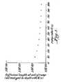
- FIG. 1is a graph showing the effect of ramp rate on the diffusion length at the end of the ramp for copper on TaN 0.62 .
- the graphshows that diffusion length is minimized at higher ramp rates. Further, it is shown that diffusion length is reduced by a factor of about 2 at the end of the temperature ramp up if the ramp is increased from about 20° C. per second to about 80° C. per second.
- Capacitance-Bias (C-V) curves of all post-cure coating materialswere determined using a mercury probe. The coating thickness was determined using the accumulation capacitance values and assuming a dielectric constant (k) of 2.85.
- FIG. 3is a Capacitance-Bias (C-V) curve of FLARE film at 250° C. for 180 seconds. The thickness of each sample was calculated to be 0.38 ⁇ m, which was in agreement with post-heating thickness calculated by the coating vendor. Therefore, none of the coating materials suffered a thickness loss after curing, which indicates that thermal decomposition, if any, was negligible for the cure cycles investigated.
Landscapes
- Engineering & Computer Science (AREA)
- Physics & Mathematics (AREA)
- Condensed Matter Physics & Semiconductors (AREA)
- General Physics & Mathematics (AREA)
- Manufacturing & Machinery (AREA)
- Computer Hardware Design (AREA)
- Microelectronics & Electronic Packaging (AREA)
- Power Engineering (AREA)
- Internal Circuitry In Semiconductor Integrated Circuit Devices (AREA)
- Inorganic Insulating Materials (AREA)
- Formation Of Insulating Films (AREA)
Abstract
Description
| TABLE 1 |
| Spin-coating Sequence |
| Step | Action | Time (sec.) | Speed (rpm) |
| 1 | Pre-dispense | 0.2 | 0 |
| 2 | Dispense | 3.0 | 3000 |
| 3 | Spread | 0.1 | 3000 |
| 4 | Thickness spin | 40.0 | 3000 |
| 5 | Backside rinse | 6.0 | 1500 |
| 6 | Edge-bead rinse | 4.0 | 1500 |
| 7 | Spin dry | 4.0 | 3000 |
| 8 | Spin dry/nozzle rinse | 1 | 3000 |
| TABLE 2 |
| Summary of FTIR Data |
| Cure Temperature | Time | |||
| (Elevated | (First Time | Absorbance peak | Fully | |
| Example | Temperature) | Interval) | at 2200 cm−1 | Cured |
| A | No cure | Bake only | 0.02 | No |
| B | 425° C. | 180 s | ˜0 | Yes |
| C | 450° C. | 30 s | 0.0077 | No |
| D | 450° C. | 60 s | ˜0 | Yes |
| E | 475° C. | 15 s | 0.0087 | No |
| F | 475° C. | 30 s | ˜0 | Yes |
| TABLE 3 |
| Diffusion Lengths for Diffusion of Copper Through Ta and TaNx |
| Cure Time | Diffusion | |||
| Diffusion Barrier | Example | Cure Temp | (sec.) | Length |
| Ta | G | 425° C. | 180 | 0.226381 |
| H | 450° C. | 60 | 0.13221 | |
| I | 475° C. | 30 | 0.094493 | |
| TaN0.62 | J | 425° C. | 180 | 0.260864 |
| K | 450° C. | 60 | 0.173842 | |
| L | 475° C. | 30 | 0.140532 | |
| TaN0.69 | M | 425° C. | 180 | 0.268202 |
| N | 450° C. | 60 | 0.183407 | |
| O | 475° C. | 30 | 0.15188 | |
| TaN0.85 | P | 425° C. | 180 | 0.279166 |
| Q | 450° C. | 60 | 0.19816 | |
| R | 475° C. | 30 | 0.169909 | |
| TaN0.99 | S | 425° C. | 180 | 0.286135 |
| T | 450° C. | 60 | 0.207822 | |
| U | 475° C. | 30 | 0.182052 | |
| TaN1.23 | V | 425° C. | 180 | 0.291476 |
| W | 450° C. | 60 | 0.215377 | |
| X | 475° C. | 30 | 0.191725 | |
Claims (34)
Priority Applications (7)
| Application Number | Priority Date | Filing Date | Title |
|---|---|---|---|
| US09/789,062US6303524B1 (en) | 2001-02-20 | 2001-02-20 | High temperature short time curing of low dielectric constant materials using rapid thermal processing techniques |
| AT02715628TATE369624T1 (en) | 2001-02-20 | 2002-01-24 | METHOD FOR HIGH-TEMPERATURE SHORT-TERM HARDENING OF LOW-DIELECTRICITY MATERIALS USING A FAST THERMAL PROCESS |
| PCT/IB2002/000210WO2002067314A2 (en) | 2001-02-20 | 2002-01-24 | High temperature short time curing of low dielectric constant materials using rapid thermal processing techniques |
| KR10-2003-7010829AKR20030074838A (en) | 2001-02-20 | 2002-01-24 | High temperature short time curing of low dielectric constant materials using rapid thermal processing techniques |
| EP02715628AEP1364397B1 (en) | 2001-02-20 | 2002-01-24 | High temperature short time curing of low dielectric constant materials using rapid thermal processing techniques |
| DE60221649TDE60221649T2 (en) | 2001-02-20 | 2002-01-24 | METHOD FOR HIGH-TEMPERATURE SHORT-TERMINATION OF MATERIALS WITH LOWER DIELECTRICITY CONSTANT USING A FAST THERMAL PROCESS |
| TW091101926ATW536759B (en) | 2001-02-20 | 2002-02-04 | High temperature short time curing of low dielectric constant materials using rapid thermal processing techniques |
Applications Claiming Priority (1)
| Application Number | Priority Date | Filing Date | Title |
|---|---|---|---|
| US09/789,062US6303524B1 (en) | 2001-02-20 | 2001-02-20 | High temperature short time curing of low dielectric constant materials using rapid thermal processing techniques |
Publications (1)
| Publication Number | Publication Date |
|---|---|
| US6303524B1true US6303524B1 (en) | 2001-10-16 |
Family
ID=25146475
Family Applications (1)
| Application Number | Title | Priority Date | Filing Date |
|---|---|---|---|
| US09/789,062Expired - LifetimeUS6303524B1 (en) | 2001-02-20 | 2001-02-20 | High temperature short time curing of low dielectric constant materials using rapid thermal processing techniques |
Country Status (7)
| Country | Link |
|---|---|
| US (1) | US6303524B1 (en) |
| EP (1) | EP1364397B1 (en) |
| KR (1) | KR20030074838A (en) |
| AT (1) | ATE369624T1 (en) |
| DE (1) | DE60221649T2 (en) |
| TW (1) | TW536759B (en) |
| WO (1) | WO2002067314A2 (en) |
Cited By (44)
| Publication number | Priority date | Publication date | Assignee | Title |
|---|---|---|---|---|
| US20030031793A1 (en)* | 2001-03-20 | 2003-02-13 | Mattson Technology, Inc. | Method for depositing a coating having a relatively high dielectric constant onto a substrate |
| US6667249B1 (en)* | 2002-03-20 | 2003-12-23 | Taiwan Semiconductor Manufacturing Company | Minimizing coating defects in low dielectric constant films |
| US20040025787A1 (en)* | 2002-04-19 | 2004-02-12 | Selbrede Steven C. | System for depositing a film onto a substrate using a low pressure gas precursor |
| US20040087122A1 (en)* | 2002-10-30 | 2004-05-06 | Taiwan Semiconductor Manufacturing Company | Adhesion enhancement between CVD dielectric and spin-on low-k silicate films |
| US20040099283A1 (en)* | 2002-11-26 | 2004-05-27 | Axcelis Technologies, Inc. | Drying process for low-k dielectric films |
| US20040104473A1 (en)* | 2002-06-25 | 2004-06-03 | Farnworth Warren M. | Semiconductor component having conductors with wire bondable metalization layers |
| US20050064726A1 (en)* | 2003-09-23 | 2005-03-24 | Jason Reid | Method of forming low-k dielectrics |
| US20060016786A1 (en)* | 2004-07-26 | 2006-01-26 | Bing-Yue Tsui | Method and apparatus for removing SiC or low k material film |
| US7018941B2 (en) | 2004-04-21 | 2006-03-28 | Applied Materials, Inc. | Post treatment of low k dielectric films |
| US20080063809A1 (en)* | 2006-09-08 | 2008-03-13 | Tokyo Electron Limited | Thermal processing system for curing dielectric films |
| US20080254619A1 (en)* | 2007-04-14 | 2008-10-16 | Tsang-Jung Lin | Method of fabricating a semiconductor device |
| US20090075491A1 (en)* | 2007-09-13 | 2009-03-19 | Tokyo Electron Limited | Method for curing a dielectric film |
| US20090226695A1 (en)* | 2008-03-06 | 2009-09-10 | Tokyo Electron Limited | Method for treating a dielectric film with infrared radiation |
| US20090227119A1 (en)* | 2008-03-06 | 2009-09-10 | Tokyo Electron Limited | Method for curing a porous low dielectric constant dielectric film |
| US20090226694A1 (en)* | 2008-03-06 | 2009-09-10 | Tokyo Electron Limited | POROUS SiCOH-CONTAINING DIELECTRIC FILM AND A METHOD OF PREPARING |
| US20090253080A1 (en)* | 2008-04-02 | 2009-10-08 | Dammel Ralph R | Photoresist Image-Forming Process Using Double Patterning |
| US20090253081A1 (en)* | 2008-04-02 | 2009-10-08 | David Abdallah | Process for Shrinking Dimensions Between Photoresist Pattern Comprising a Pattern Hardening Step |
| US7622378B2 (en) | 2005-11-09 | 2009-11-24 | Tokyo Electron Limited | Multi-step system and method for curing a dielectric film |
| US20100040838A1 (en)* | 2008-08-15 | 2010-02-18 | Abdallah David J | Hardmask Process for Forming a Reverse Tone Image |
| US20100065758A1 (en)* | 2008-09-16 | 2010-03-18 | Tokyo Electron Limited | Dielectric material treatment system and method of operating |
| US20100068897A1 (en)* | 2008-09-16 | 2010-03-18 | Tokyo Electron Limited | Dielectric treatment platform for dielectric film deposition and curing |
| US20100065759A1 (en)* | 2008-09-16 | 2010-03-18 | Tokyo Electron Limited | Dielectric treatment module using scanning ir radiation source |
| US20100183851A1 (en)* | 2009-01-21 | 2010-07-22 | Yi Cao | Photoresist Image-forming Process Using Double Patterning |
| US20100203299A1 (en)* | 2009-02-10 | 2010-08-12 | David Abdallah | Hardmask Process for Forming a Reverse Tone Image Using Polysilazane |
| US20100273277A1 (en)* | 2009-04-23 | 2010-10-28 | Micron Technology, Inc. | Rapid thermal processing systems and methods for treating microelectronic substrates |
| US7977256B2 (en) | 2008-03-06 | 2011-07-12 | Tokyo Electron Limited | Method for removing a pore-generating material from an uncured low-k dielectric film |
| US20110232677A1 (en)* | 2010-03-29 | 2011-09-29 | Tokyo Electron Limited | Method for cleaning low-k dielectrics |
| US20130084394A1 (en)* | 2010-05-28 | 2013-04-04 | Jsr Corporation | Insulation pattern-forming method and insulation pattern-forming material |
| US20140127901A1 (en)* | 2012-11-08 | 2014-05-08 | Taiwan Semiconductor Manufacturing Company, Ltd. | Low-k damage free integration scheme for copper interconnects |
| WO2021034882A1 (en)* | 2019-08-21 | 2021-02-25 | Ticona Llc | Polymer composition for use in an antenna system |
| US10985071B1 (en)* | 2019-10-30 | 2021-04-20 | United Microelectronics Corp. | Gate oxide forming process |
| RU2752125C1 (en)* | 2020-11-20 | 2021-07-23 | Федеральное государственное бюджетное образовательное учреждение высшего образования "Кабардино-Балкарский государственный университет им. Х.М. Бербекова" (КБГУ) | Method for manufacturing semiconductor device |
| US11258184B2 (en) | 2019-08-21 | 2022-02-22 | Ticona Llc | Antenna system including a polymer composition having a low dissipation factor |
| US11555113B2 (en) | 2019-09-10 | 2023-01-17 | Ticona Llc | Liquid crystalline polymer composition |
| US11646760B2 (en) | 2019-09-23 | 2023-05-09 | Ticona Llc | RF filter for use at 5G frequencies |
| US11721888B2 (en) | 2019-11-11 | 2023-08-08 | Ticona Llc | Antenna cover including a polymer composition having a low dielectric constant and dissipation factor |
| US11729908B2 (en) | 2020-02-26 | 2023-08-15 | Ticona Llc | Circuit structure |
| US11728559B2 (en) | 2021-02-18 | 2023-08-15 | Ticona Llc | Polymer composition for use in an antenna system |
| US11917753B2 (en) | 2019-09-23 | 2024-02-27 | Ticona Llc | Circuit board for use at 5G frequencies |
| US11912817B2 (en) | 2019-09-10 | 2024-02-27 | Ticona Llc | Polymer composition for laser direct structuring |
| US12142820B2 (en) | 2019-09-10 | 2024-11-12 | Ticona Llc | 5G system containing a polymer composition |
| US12209164B2 (en) | 2019-09-10 | 2025-01-28 | Ticona Llc | Polymer composition and film for use in 5G applications |
| US12294185B2 (en) | 2019-09-10 | 2025-05-06 | Ticona Llc | Electrical connector formed from a polymer composition having a low dielectric constant and dissipation factor |
| US12441879B2 (en) | 2020-08-18 | 2025-10-14 | Ticona Llc | Polymer composition for laser direct structuring |
Citations (17)
| Publication number | Priority date | Publication date | Assignee | Title |
|---|---|---|---|---|
| US4331485A (en) | 1980-03-03 | 1982-05-25 | Arnon Gat | Method for heat treating semiconductor material using high intensity CW lamps |
| US4356384A (en) | 1980-03-03 | 1982-10-26 | Arnon Gat | Method and means for heat treating semiconductor material using high intensity CW lamps |
| US4680451A (en) | 1985-07-29 | 1987-07-14 | A. G. Associates | Apparatus using high intensity CW lamps for improved heat treating of semiconductor wafers |
| US5238878A (en) | 1992-02-18 | 1993-08-24 | Nec Corporation | Film forming method by spin coating in production of semiconductor device |
| US5358740A (en) | 1992-06-24 | 1994-10-25 | Massachusetts Institute Of Technology | Method for low pressure spin coating and low pressure spin coating apparatus |
| WO1995032604A1 (en) | 1994-05-23 | 1995-11-30 | General Electric Company | Processing low dielectric constant materials for high speed electronics |
| US5705232A (en) | 1994-09-20 | 1998-01-06 | Texas Instruments Incorporated | In-situ coat, bake and cure of dielectric material processing system for semiconductor manufacturing |
| US5965047A (en) | 1997-10-24 | 1999-10-12 | Steag Ast | Rapid thermal processing (RTP) system with rotating substrate |
| US5972803A (en) | 1994-04-20 | 1999-10-26 | Texas Instruments Incorporated | High throughput optical curing process for semiconductor device manufacturing |
| EP0971400A2 (en) | 1998-07-10 | 2000-01-12 | Dow Corning Corporation | Method for producing low dielectric coatings from hydrogen silsesquioxane resin |
| US6033728A (en) | 1993-05-13 | 2000-03-07 | Fujitsu Limited | Apparatus for spin coating, a method for spin coating and a method for manufacturing semiconductor device |
| US6051512A (en) | 1997-04-11 | 2000-04-18 | Steag Rtp Systems | Apparatus and method for rapid thermal processing (RTP) of a plurality of semiconductor wafers |
| US6066574A (en) | 1998-11-06 | 2000-05-23 | Advanced Micro Devices, Inc. | Hot plate cure process for BCB low k interlevel dielectric |
| US6107357A (en) | 1999-11-16 | 2000-08-22 | International Business Machines Corporatrion | Dielectric compositions and method for their manufacture |
| US6133550A (en) | 1996-03-22 | 2000-10-17 | Sandia Corporation | Method and apparatus for thermal processing of semiconductor substrates |
| US6214748B1 (en)* | 1997-05-28 | 2001-04-10 | Dow Corning Toray Silicone Co. | Semiconductor device and method for the fabrication thereof |
| US6225238B1 (en)* | 1999-06-07 | 2001-05-01 | Allied Signal Inc | Low dielectric constant polyorganosilicon coatings generated from polycarbosilanes |
Family Cites Families (3)
| Publication number | Priority date | Publication date | Assignee | Title |
|---|---|---|---|---|
| US3619231A (en)* | 1965-10-15 | 1971-11-09 | Anchor Post Prod | Continuous metal coating process with fusible pulverulent materials |
| GB1549346A (en)* | 1975-05-12 | 1979-08-08 | Armco Inc | Method of coating elongated metallic members with a thermosetting plastics coating |
| JPH02303131A (en)* | 1989-05-18 | 1990-12-17 | Oki Electric Ind Co Ltd | Insulating film formation method |
- 2001
- 2001-02-20USUS09/789,062patent/US6303524B1/ennot_activeExpired - Lifetime
- 2002
- 2002-01-24ATAT02715628Tpatent/ATE369624T1/ennot_activeIP Right Cessation
- 2002-01-24WOPCT/IB2002/000210patent/WO2002067314A2/enactiveIP Right Grant
- 2002-01-24DEDE60221649Tpatent/DE60221649T2/ennot_activeExpired - Fee Related
- 2002-01-24EPEP02715628Apatent/EP1364397B1/ennot_activeExpired - Lifetime
- 2002-01-24KRKR10-2003-7010829Apatent/KR20030074838A/ennot_activeWithdrawn
- 2002-02-04TWTW091101926Apatent/TW536759B/ennot_activeIP Right Cessation
Patent Citations (17)
| Publication number | Priority date | Publication date | Assignee | Title |
|---|---|---|---|---|
| US4331485A (en) | 1980-03-03 | 1982-05-25 | Arnon Gat | Method for heat treating semiconductor material using high intensity CW lamps |
| US4356384A (en) | 1980-03-03 | 1982-10-26 | Arnon Gat | Method and means for heat treating semiconductor material using high intensity CW lamps |
| US4680451A (en) | 1985-07-29 | 1987-07-14 | A. G. Associates | Apparatus using high intensity CW lamps for improved heat treating of semiconductor wafers |
| US5238878A (en) | 1992-02-18 | 1993-08-24 | Nec Corporation | Film forming method by spin coating in production of semiconductor device |
| US5358740A (en) | 1992-06-24 | 1994-10-25 | Massachusetts Institute Of Technology | Method for low pressure spin coating and low pressure spin coating apparatus |
| US6033728A (en) | 1993-05-13 | 2000-03-07 | Fujitsu Limited | Apparatus for spin coating, a method for spin coating and a method for manufacturing semiconductor device |
| US5972803A (en) | 1994-04-20 | 1999-10-26 | Texas Instruments Incorporated | High throughput optical curing process for semiconductor device manufacturing |
| WO1995032604A1 (en) | 1994-05-23 | 1995-11-30 | General Electric Company | Processing low dielectric constant materials for high speed electronics |
| US5705232A (en) | 1994-09-20 | 1998-01-06 | Texas Instruments Incorporated | In-situ coat, bake and cure of dielectric material processing system for semiconductor manufacturing |
| US6133550A (en) | 1996-03-22 | 2000-10-17 | Sandia Corporation | Method and apparatus for thermal processing of semiconductor substrates |
| US6051512A (en) | 1997-04-11 | 2000-04-18 | Steag Rtp Systems | Apparatus and method for rapid thermal processing (RTP) of a plurality of semiconductor wafers |
| US6214748B1 (en)* | 1997-05-28 | 2001-04-10 | Dow Corning Toray Silicone Co. | Semiconductor device and method for the fabrication thereof |
| US5965047A (en) | 1997-10-24 | 1999-10-12 | Steag Ast | Rapid thermal processing (RTP) system with rotating substrate |
| EP0971400A2 (en) | 1998-07-10 | 2000-01-12 | Dow Corning Corporation | Method for producing low dielectric coatings from hydrogen silsesquioxane resin |
| US6066574A (en) | 1998-11-06 | 2000-05-23 | Advanced Micro Devices, Inc. | Hot plate cure process for BCB low k interlevel dielectric |
| US6225238B1 (en)* | 1999-06-07 | 2001-05-01 | Allied Signal Inc | Low dielectric constant polyorganosilicon coatings generated from polycarbosilanes |
| US6107357A (en) | 1999-11-16 | 2000-08-22 | International Business Machines Corporatrion | Dielectric compositions and method for their manufacture |
Non-Patent Citations (4)
| Title |
|---|
| Allied Signal FLARE(TM) Product Bulletin (2/99). |
| Allied Signal FLARE™ Product Bulletin (2/99). |
| Dow Chemical CYCLOTENE 4000 Series Advanced Eletronic Resins (Photo BCB) Revised: May 3, 1999 technical bulletin. |
| J. Lin and C. Lee, "Grain Boundary Diffusion of Copper in Tantabum Nitride Thin Films," J. Electrochem Soc., 146 (9) 3466-3471 (1999). |
Cited By (77)
| Publication number | Priority date | Publication date | Assignee | Title |
|---|---|---|---|---|
| US20030031793A1 (en)* | 2001-03-20 | 2003-02-13 | Mattson Technology, Inc. | Method for depositing a coating having a relatively high dielectric constant onto a substrate |
| US6884719B2 (en) | 2001-03-20 | 2005-04-26 | Mattson Technology, Inc. | Method for depositing a coating having a relatively high dielectric constant onto a substrate |
| US6667249B1 (en)* | 2002-03-20 | 2003-12-23 | Taiwan Semiconductor Manufacturing Company | Minimizing coating defects in low dielectric constant films |
| US20040025787A1 (en)* | 2002-04-19 | 2004-02-12 | Selbrede Steven C. | System for depositing a film onto a substrate using a low pressure gas precursor |
| US7132750B2 (en) | 2002-06-25 | 2006-11-07 | Micron Technology, Inc. | Semiconductor component having conductors with wire bondable metalization layers |
| US20040104473A1 (en)* | 2002-06-25 | 2004-06-03 | Farnworth Warren M. | Semiconductor component having conductors with wire bondable metalization layers |
| US6784544B1 (en) | 2002-06-25 | 2004-08-31 | Micron Technology, Inc. | Semiconductor component having conductors with wire bondable metalization layers |
| US20050017358A1 (en)* | 2002-06-25 | 2005-01-27 | Farnworth Warren M. | Semiconductor component having conductors with wire bondable metalization layers |
| US20070048999A1 (en)* | 2002-06-25 | 2007-03-01 | Farnworth Warren M | Method for fabricating semiconductor component having conductors and bonding pads with wire bondable surfaces and selected thickness |
| US6887787B2 (en) | 2002-06-25 | 2005-05-03 | Micron Technology, Inc. | Method for fabricating semiconductor components with conductors having wire bondable metalization layers |
| US20040087122A1 (en)* | 2002-10-30 | 2004-05-06 | Taiwan Semiconductor Manufacturing Company | Adhesion enhancement between CVD dielectric and spin-on low-k silicate films |
| US6812135B2 (en) | 2002-10-30 | 2004-11-02 | Taiwan Semiconductor Manufacturing Company, Ltd | Adhesion enhancement between CVD dielectric and spin-on low-k silicate films |
| US20040099283A1 (en)* | 2002-11-26 | 2004-05-27 | Axcelis Technologies, Inc. | Drying process for low-k dielectric films |
| US20050064726A1 (en)* | 2003-09-23 | 2005-03-24 | Jason Reid | Method of forming low-k dielectrics |
| US7622399B2 (en)* | 2003-09-23 | 2009-11-24 | Silecs Oy | Method of forming low-k dielectrics using a rapid curing process |
| US7018941B2 (en) | 2004-04-21 | 2006-03-28 | Applied Materials, Inc. | Post treatment of low k dielectric films |
| US20060016786A1 (en)* | 2004-07-26 | 2006-01-26 | Bing-Yue Tsui | Method and apparatus for removing SiC or low k material film |
| US7622378B2 (en) | 2005-11-09 | 2009-11-24 | Tokyo Electron Limited | Multi-step system and method for curing a dielectric film |
| US9184047B2 (en) | 2005-11-09 | 2015-11-10 | Tokyo Electron Limited | Multi-step system and method for curing a dielectric film |
| US10068765B2 (en)* | 2005-11-09 | 2018-09-04 | Tokyo Electron Limited | Multi-step system and method for curing a dielectric film |
| US8642488B2 (en) | 2005-11-09 | 2014-02-04 | Tokyo Electron Limited | Multi-step system and method for curing a dielectric film |
| CN103489813A (en)* | 2005-11-09 | 2014-01-01 | 东京毅力科创株式会社 | Multi-step system and method for curing a dielectric film |
| US9443725B2 (en) | 2005-11-09 | 2016-09-13 | Tokyo Electron Limited | Multi-step system and method for curing a dielectric film |
| US20100041248A1 (en)* | 2005-11-09 | 2010-02-18 | Tokyo Electron Limited | Multi-step system and method for curing a dielectric film |
| US20080063809A1 (en)* | 2006-09-08 | 2008-03-13 | Tokyo Electron Limited | Thermal processing system for curing dielectric films |
| US8956457B2 (en) | 2006-09-08 | 2015-02-17 | Tokyo Electron Limited | Thermal processing system for curing dielectric films |
| US20080254619A1 (en)* | 2007-04-14 | 2008-10-16 | Tsang-Jung Lin | Method of fabricating a semiconductor device |
| US20090075491A1 (en)* | 2007-09-13 | 2009-03-19 | Tokyo Electron Limited | Method for curing a dielectric film |
| US20090226694A1 (en)* | 2008-03-06 | 2009-09-10 | Tokyo Electron Limited | POROUS SiCOH-CONTAINING DIELECTRIC FILM AND A METHOD OF PREPARING |
| US7858533B2 (en) | 2008-03-06 | 2010-12-28 | Tokyo Electron Limited | Method for curing a porous low dielectric constant dielectric film |
| US20090227119A1 (en)* | 2008-03-06 | 2009-09-10 | Tokyo Electron Limited | Method for curing a porous low dielectric constant dielectric film |
| US20090226695A1 (en)* | 2008-03-06 | 2009-09-10 | Tokyo Electron Limited | Method for treating a dielectric film with infrared radiation |
| US7977256B2 (en) | 2008-03-06 | 2011-07-12 | Tokyo Electron Limited | Method for removing a pore-generating material from an uncured low-k dielectric film |
| US20090253080A1 (en)* | 2008-04-02 | 2009-10-08 | Dammel Ralph R | Photoresist Image-Forming Process Using Double Patterning |
| US20090253081A1 (en)* | 2008-04-02 | 2009-10-08 | David Abdallah | Process for Shrinking Dimensions Between Photoresist Pattern Comprising a Pattern Hardening Step |
| US20100040838A1 (en)* | 2008-08-15 | 2010-02-18 | Abdallah David J | Hardmask Process for Forming a Reverse Tone Image |
| US20100065759A1 (en)* | 2008-09-16 | 2010-03-18 | Tokyo Electron Limited | Dielectric treatment module using scanning ir radiation source |
| US20100068897A1 (en)* | 2008-09-16 | 2010-03-18 | Tokyo Electron Limited | Dielectric treatment platform for dielectric film deposition and curing |
| US20100065758A1 (en)* | 2008-09-16 | 2010-03-18 | Tokyo Electron Limited | Dielectric material treatment system and method of operating |
| US8895942B2 (en) | 2008-09-16 | 2014-11-25 | Tokyo Electron Limited | Dielectric treatment module using scanning IR radiation source |
| US20100183851A1 (en)* | 2009-01-21 | 2010-07-22 | Yi Cao | Photoresist Image-forming Process Using Double Patterning |
| US20100203299A1 (en)* | 2009-02-10 | 2010-08-12 | David Abdallah | Hardmask Process for Forming a Reverse Tone Image Using Polysilazane |
| US8084186B2 (en) | 2009-02-10 | 2011-12-27 | Az Electronic Materials Usa Corp. | Hardmask process for forming a reverse tone image using polysilazane |
| US20100273277A1 (en)* | 2009-04-23 | 2010-10-28 | Micron Technology, Inc. | Rapid thermal processing systems and methods for treating microelectronic substrates |
| US8426763B2 (en) | 2009-04-23 | 2013-04-23 | Micron Technology, Inc. | Rapid thermal processing systems and methods for treating microelectronic substrates |
| US8822877B2 (en) | 2009-04-23 | 2014-09-02 | Micron Technology, Inc. | Rapid thermal processing systems and methods for treating microelectronic substrates |
| US20110237080A1 (en)* | 2010-03-29 | 2011-09-29 | Tokyo Electron Limited | Method for integrating low-k dielectrics |
| TWI464805B (en)* | 2010-03-29 | 2014-12-11 | Tokyo Electron Ltd | Method for integrating low-k dielectrics |
| US9017933B2 (en) | 2010-03-29 | 2015-04-28 | Tokyo Electron Limited | Method for integrating low-k dielectrics |
| US8242460B2 (en) | 2010-03-29 | 2012-08-14 | Tokyo Electron Limited | Ultraviolet treatment apparatus |
| US20110233430A1 (en)* | 2010-03-29 | 2011-09-29 | Tokyo Electron Limited | Ultraviolet treatment apparatus |
| US20110232677A1 (en)* | 2010-03-29 | 2011-09-29 | Tokyo Electron Limited | Method for cleaning low-k dielectrics |
| US20130084394A1 (en)* | 2010-05-28 | 2013-04-04 | Jsr Corporation | Insulation pattern-forming method and insulation pattern-forming material |
| US9126231B2 (en)* | 2010-05-28 | 2015-09-08 | Jsr Corporation | Insulation pattern-forming method and insulation pattern-forming material |
| US20140127901A1 (en)* | 2012-11-08 | 2014-05-08 | Taiwan Semiconductor Manufacturing Company, Ltd. | Low-k damage free integration scheme for copper interconnects |
| WO2021034882A1 (en)* | 2019-08-21 | 2021-02-25 | Ticona Llc | Polymer composition for use in an antenna system |
| US11258184B2 (en) | 2019-08-21 | 2022-02-22 | Ticona Llc | Antenna system including a polymer composition having a low dissipation factor |
| US11637365B2 (en) | 2019-08-21 | 2023-04-25 | Ticona Llc | Polymer composition for use in an antenna system |
| US11705641B2 (en) | 2019-08-21 | 2023-07-18 | Ticoan Llc | Antenna system including a polymer composition having a low dissipation factor |
| US12136762B2 (en) | 2019-08-21 | 2024-11-05 | Ticona Llc | Polymer composition for use in an antenna system |
| US12428522B2 (en) | 2019-09-10 | 2025-09-30 | Ticona Llc | Polymer composition for laser direct structuring |
| US12294185B2 (en) | 2019-09-10 | 2025-05-06 | Ticona Llc | Electrical connector formed from a polymer composition having a low dielectric constant and dissipation factor |
| US11555113B2 (en) | 2019-09-10 | 2023-01-17 | Ticona Llc | Liquid crystalline polymer composition |
| US11912817B2 (en) | 2019-09-10 | 2024-02-27 | Ticona Llc | Polymer composition for laser direct structuring |
| US12209164B2 (en) | 2019-09-10 | 2025-01-28 | Ticona Llc | Polymer composition and film for use in 5G applications |
| US12142820B2 (en) | 2019-09-10 | 2024-11-12 | Ticona Llc | 5G system containing a polymer composition |
| US11646760B2 (en) | 2019-09-23 | 2023-05-09 | Ticona Llc | RF filter for use at 5G frequencies |
| US11917753B2 (en) | 2019-09-23 | 2024-02-27 | Ticona Llc | Circuit board for use at 5G frequencies |
| US12107617B2 (en) | 2019-09-23 | 2024-10-01 | Ticona Llc | RF filter for use at 5G frequencies |
| US10985071B1 (en)* | 2019-10-30 | 2021-04-20 | United Microelectronics Corp. | Gate oxide forming process |
| US11721888B2 (en) | 2019-11-11 | 2023-08-08 | Ticona Llc | Antenna cover including a polymer composition having a low dielectric constant and dissipation factor |
| US12035467B2 (en) | 2020-02-26 | 2024-07-09 | Ticona Llc | Circuit structure |
| US11729908B2 (en) | 2020-02-26 | 2023-08-15 | Ticona Llc | Circuit structure |
| US12441879B2 (en) | 2020-08-18 | 2025-10-14 | Ticona Llc | Polymer composition for laser direct structuring |
| RU2752125C1 (en)* | 2020-11-20 | 2021-07-23 | Федеральное государственное бюджетное образовательное учреждение высшего образования "Кабардино-Балкарский государственный университет им. Х.М. Бербекова" (КБГУ) | Method for manufacturing semiconductor device |
| US11728559B2 (en) | 2021-02-18 | 2023-08-15 | Ticona Llc | Polymer composition for use in an antenna system |
| US12230865B2 (en) | 2021-02-18 | 2025-02-18 | Ticona Llc | Polymer composition for use in an antenna system |
Also Published As
| Publication number | Publication date |
|---|---|
| WO2002067314A2 (en) | 2002-08-29 |
| DE60221649T2 (en) | 2008-05-21 |
| EP1364397A2 (en) | 2003-11-26 |
| WO2002067314A3 (en) | 2002-12-05 |
| TW536759B (en) | 2003-06-11 |
| DE60221649D1 (en) | 2007-09-20 |
| KR20030074838A (en) | 2003-09-19 |
| ATE369624T1 (en) | 2007-08-15 |
| EP1364397B1 (en) | 2007-08-08 |
Similar Documents
| Publication | Publication Date | Title |
|---|---|---|
| US6303524B1 (en) | High temperature short time curing of low dielectric constant materials using rapid thermal processing techniques | |
| US8242028B1 (en) | UV treatment of etch stop and hard mask films for selectivity and hermeticity enhancement | |
| US10068765B2 (en) | Multi-step system and method for curing a dielectric film | |
| US6080526A (en) | Integration of low-k polymers into interlevel dielectrics using controlled electron-beam radiation | |
| US7666754B2 (en) | Method and system for forming an air gap structure | |
| CN100530564C (en) | Method of sealing porous low-k dielectric materials | |
| JP3568537B2 (en) | Electron beam processed film for microelectronic structure | |
| KR100878170B1 (en) | Dual Frequency Plasma Chemical Vapor Deposition of Silicon Carbide Layers | |
| US9589892B2 (en) | Interconnect structure and method of forming the same | |
| US5457073A (en) | Multi-level interconnection CMOS devices with SOG | |
| US6559071B2 (en) | Process for producing dielectric thin films | |
| US20090075491A1 (en) | Method for curing a dielectric film | |
| US20060102977A1 (en) | Low temperature process for polysilazane oxidation/densification | |
| US20030008518A1 (en) | Method of avoiding dielectric layer deterioation with a low dielectric constant | |
| US7829268B2 (en) | Method for air gap formation using UV-decomposable materials | |
| US7557035B1 (en) | Method of forming semiconductor devices by microwave curing of low-k dielectric films | |
| US6268294B1 (en) | Method of protecting a low-K dielectric material | |
| KR100489456B1 (en) | Semiconductor device and its manufacturing method | |
| US20050153533A1 (en) | Semiconductor manufacturing method and semiconductor manufacturing apparatus | |
| US9004914B2 (en) | Method of and apparatus for active energy assist baking | |
| US20100301495A1 (en) | Semiconductor device and method for manufacturing same | |
| US20200203154A1 (en) | Oxidation reduction for sioc film | |
| Zhao et al. | A novel sub-half micron Al-Cu via plug interconnect using low dielectric constant material as inter-level dielectric |
Legal Events
| Date | Code | Title | Description |
|---|---|---|---|
| AS | Assignment | Owner name:MATTSON TECHNOLOGY, INC., CALIFORNIA Free format text:ASSIGNMENT OF ASSIGNORS INTEREST;ASSIGNORS:SHARANGPANI, RAHUL;TAY, SING-PIN;REEL/FRAME:011567/0033 Effective date:20010206 | |
| AS | Assignment | Owner name:MATTSON THERMAL PRODUCTS, INC., CALIFORNIA Free format text:ASSIGNMENT OF ASSIGNORS INTEREST;ASSIGNOR:MATTSON TECHNOLOGY, INC.;REEL/FRAME:012112/0355 Effective date:20010814 | |
| STCF | Information on status: patent grant | Free format text:PATENTED CASE | |
| FEPP | Fee payment procedure | Free format text:PAYOR NUMBER ASSIGNED (ORIGINAL EVENT CODE: ASPN); ENTITY STATUS OF PATENT OWNER: LARGE ENTITY | |
| FPAY | Fee payment | Year of fee payment:4 | |
| FPAY | Fee payment | Year of fee payment:8 | |
| FEPP | Fee payment procedure | Free format text:PAT HOLDER CLAIMS SMALL ENTITY STATUS, ENTITY STATUS SET TO SMALL (ORIGINAL EVENT CODE: LTOS); ENTITY STATUS OF PATENT OWNER: LARGE ENTITY | |
| FPAY | Fee payment | Year of fee payment:12 | |
| FEPP | Fee payment procedure | Free format text:ENTITY STATUS SET TO UNDISCOUNTED (ORIGINAL EVENT CODE: BIG.) | |
| AS | Assignment | Owner name:MATTSON TECHNOLOGY, INC., CALIFORNIA Free format text:CERTIFICATE OF DISSOLUTION;ASSIGNOR:MATTSON THERMAL PRODUCTS, INC.;REEL/FRAME:045405/0116 Effective date:20070202 | |
| AS | Assignment | Owner name:EAST WEST BANK, CALIFORNIA Free format text:SECURITY INTEREST;ASSIGNOR:MATTSON TECHNOLOGY, INC.;REEL/FRAME:046956/0348 Effective date:20180821 | |
| AS | Assignment | Owner name:MATTSON TECHNOLOGY, INC., CALIFORNIA Free format text:ASSIGNMENT OF ASSIGNORS INTEREST;ASSIGNOR:MATTSON TECHNOLOGY, INC.;REEL/FRAME:050582/0796 Effective date:20190925 Owner name:BEIJING E-TOWN SEMICONDUCTOR TECHNOLOGY, CO., LTD, Free format text:ASSIGNMENT OF ASSIGNORS INTEREST;ASSIGNOR:MATTSON TECHNOLOGY, INC.;REEL/FRAME:050582/0796 Effective date:20190925 Owner name:BEIJING E-TOWN SEMICONDUCTOR TECHNOLOGY, CO., LTD, CHINA Free format text:ASSIGNMENT OF ASSIGNORS INTEREST;ASSIGNOR:MATTSON TECHNOLOGY, INC.;REEL/FRAME:050582/0796 Effective date:20190925 | |
| AS | Assignment | Owner name:MATTSON TECHNOLOGY, INC., CALIFORNIA Free format text:RELEASE BY SECURED PARTY;ASSIGNOR:EAST WEST BANK;REEL/FRAME:055950/0452 Effective date:20210415 |