US6303479B1 - Method of manufacturing a short-channel FET with Schottky-barrier source and drain contacts - Google Patents
Method of manufacturing a short-channel FET with Schottky-barrier source and drain contactsDownload PDFInfo
- Publication number
- US6303479B1 US6303479B1US09/465,357US46535799AUS6303479B1US 6303479 B1US6303479 B1US 6303479B1US 46535799 AUS46535799 AUS 46535799AUS 6303479 B1US6303479 B1US 6303479B1
- Authority
- US
- United States
- Prior art keywords
- schottky
- channel
- semiconductor substrate
- source
- drain
- Prior art date
- Legal status (The legal status is an assumption and is not a legal conclusion. Google has not performed a legal analysis and makes no representation as to the accuracy of the status listed.)
- Expired - Lifetime
Links
- 238000004519manufacturing processMethods0.000titleclaimsabstractdescription38
- 238000000034methodMethods0.000claimsabstractdescription88
- 239000000758substrateSubstances0.000claimsabstractdescription62
- 239000002019doping agentSubstances0.000claimsabstractdescription53
- 239000004065semiconductorSubstances0.000claimsabstractdescription44
- 229910052751metalInorganic materials0.000claimsdescription40
- 239000002184metalSubstances0.000claimsdescription40
- 230000008569processEffects0.000claimsdescription24
- 229910021332silicideInorganic materials0.000claimsdescription18
- FVBUAEGBCNSCDD-UHFFFAOYSA-Nsilicide(4-)Chemical compound[Si-4]FVBUAEGBCNSCDD-UHFFFAOYSA-N0.000claimsdescription14
- 239000010408filmSubstances0.000claimsdescription11
- ZOXJGFHDIHLPTG-UHFFFAOYSA-NBoronChemical compound[B]ZOXJGFHDIHLPTG-UHFFFAOYSA-N0.000claimsdescription10
- KDLHZDBZIXYQEI-UHFFFAOYSA-NPalladiumChemical compound[Pd]KDLHZDBZIXYQEI-UHFFFAOYSA-N0.000claimsdescription10
- RQNWIZPPADIBDY-UHFFFAOYSA-Narsenic atomChemical compound[As]RQNWIZPPADIBDY-UHFFFAOYSA-N0.000claimsdescription10
- 229910052796boronInorganic materials0.000claimsdescription10
- BHEPBYXIRTUNPN-UHFFFAOYSA-Nhydridophosphorus(.) (triplet)Chemical compound[PH]BHEPBYXIRTUNPN-UHFFFAOYSA-N0.000claimsdescription10
- 229910052785arsenicInorganic materials0.000claimsdescription9
- APFVFJFRJDLVQX-UHFFFAOYSA-Nindium atomChemical compound[In]APFVFJFRJDLVQX-UHFFFAOYSA-N0.000claimsdescription9
- 229910052738indiumInorganic materials0.000claimsdescription8
- ZXEYZECDXFPJRJ-UHFFFAOYSA-N$l^{3}-silane;platinumChemical compound[SiH3].[Pt]ZXEYZECDXFPJRJ-UHFFFAOYSA-N0.000claimsdescription7
- 238000005530etchingMethods0.000claimsdescription7
- 229910021339platinum silicideInorganic materials0.000claimsdescription7
- 238000000151depositionMethods0.000claimsdescription6
- GYHNNYVSQQEPJS-UHFFFAOYSA-NGalliumChemical compound[Ga]GYHNNYVSQQEPJS-UHFFFAOYSA-N0.000claimsdescription5
- 229910052787antimonyInorganic materials0.000claimsdescription5
- WATWJIUSRGPENY-UHFFFAOYSA-Nantimony atomChemical compound[Sb]WATWJIUSRGPENY-UHFFFAOYSA-N0.000claimsdescription5
- 229910052733galliumInorganic materials0.000claimsdescription5
- 229910052741iridiumInorganic materials0.000claimsdescription5
- GKOZUEZYRPOHIO-UHFFFAOYSA-Niridium atomChemical compound[Ir]GKOZUEZYRPOHIO-UHFFFAOYSA-N0.000claimsdescription5
- 229910052763palladiumInorganic materials0.000claimsdescription5
- 229910052761rare earth metalInorganic materials0.000claimsdescription5
- 150000002910rare earth metalsChemical class0.000claimsdescription5
- 238000000059patterningMethods0.000claimsdescription4
- 230000001105regulatory effectEffects0.000claimsdescription4
- 239000010409thin filmSubstances0.000claimsdescription3
- 238000000137annealingMethods0.000claims2
- -1lndiumChemical compound0.000claims1
- 230000005669field effectEffects0.000abstractdescription4
- XUIMIQQOPSSXEZ-UHFFFAOYSA-NSiliconChemical compound[Si]XUIMIQQOPSSXEZ-UHFFFAOYSA-N0.000description28
- 229910052710siliconInorganic materials0.000description26
- 239000010703siliconSubstances0.000description26
- 239000007943implantSubstances0.000description21
- 125000001475halogen functional groupChemical group0.000description16
- 230000008901benefitEffects0.000description12
- 230000003071parasitic effectEffects0.000description12
- 230000004888barrier functionEffects0.000description11
- 239000012535impuritySubstances0.000description11
- 238000005516engineering processMethods0.000description8
- 230000009467reductionEffects0.000description7
- 238000011065in-situ storageMethods0.000description6
- 150000002739metalsChemical class0.000description5
- 229910052691ErbiumInorganic materials0.000description4
- 229910045601alloyInorganic materials0.000description4
- 239000000956alloySubstances0.000description4
- 125000004429atomChemical group0.000description4
- 238000013461designMethods0.000description4
- 230000000694effectsEffects0.000description4
- UYAHIZSMUZPPFV-UHFFFAOYSA-NerbiumChemical compound[Er]UYAHIZSMUZPPFV-UHFFFAOYSA-N0.000description4
- BASFCYQUMIYNBI-UHFFFAOYSA-NplatinumChemical compound[Pt]BASFCYQUMIYNBI-UHFFFAOYSA-N0.000description4
- 238000001228spectrumMethods0.000description4
- VLJQDHDVZJXNQL-UHFFFAOYSA-N4-methyl-n-(oxomethylidene)benzenesulfonamideChemical compoundCC1=CC=C(S(=O)(=O)N=C=O)C=C1VLJQDHDVZJXNQL-UHFFFAOYSA-N0.000description3
- 238000013459approachMethods0.000description3
- 238000010586diagramMethods0.000description3
- 230000008030eliminationEffects0.000description3
- 238000003379elimination reactionMethods0.000description3
- 238000005468ion implantationMethods0.000description3
- 238000001459lithographyMethods0.000description3
- 239000000463materialSubstances0.000description3
- 229910021340platinum monosilicideInorganic materials0.000description3
- 230000005855radiationEffects0.000description3
- KRHYYFGTRYWZRS-UHFFFAOYSA-NFluoraneChemical compoundFKRHYYFGTRYWZRS-UHFFFAOYSA-N0.000description2
- VYPSYNLAJGMNEJ-UHFFFAOYSA-NSilicium dioxideChemical compoundO=[Si]=OVYPSYNLAJGMNEJ-UHFFFAOYSA-N0.000description2
- 229910052697platinumInorganic materials0.000description2
- 238000011160researchMethods0.000description2
- 239000000126substanceSubstances0.000description2
- 230000026676system processEffects0.000description2
- 238000012935AveragingMethods0.000description1
- 229910018999CoSi2Inorganic materials0.000description1
- 206010010144Completed suicideDiseases0.000description1
- GRYLNZFGIOXLOG-UHFFFAOYSA-NNitric acidChemical compoundO[N+]([O-])=OGRYLNZFGIOXLOG-UHFFFAOYSA-N0.000description1
- RTAQQCXQSZGOHL-UHFFFAOYSA-NTitaniumChemical compound[Ti]RTAQQCXQSZGOHL-UHFFFAOYSA-N0.000description1
- 230000002547anomalous effectEffects0.000description1
- 230000003466anti-cipated effectEffects0.000description1
- QZPSXPBJTPJTSZ-UHFFFAOYSA-Naqua regiaChemical compoundCl.O[N+]([O-])=OQZPSXPBJTPJTSZ-UHFFFAOYSA-N0.000description1
- 230000009286beneficial effectEffects0.000description1
- 230000015572biosynthetic processEffects0.000description1
- 239000002800charge carrierSubstances0.000description1
- 238000006243chemical reactionMethods0.000description1
- 239000003795chemical substances by applicationSubstances0.000description1
- 229910017052cobaltInorganic materials0.000description1
- 239000010941cobaltSubstances0.000description1
- GUTLYIVDDKVIGB-UHFFFAOYSA-Ncobalt atomChemical compound[Co]GUTLYIVDDKVIGB-UHFFFAOYSA-N0.000description1
- 230000000295complement effectEffects0.000description1
- 239000004020conductorSubstances0.000description1
- 230000003247decreasing effectEffects0.000description1
- 230000007812deficiencyEffects0.000description1
- 230000002939deleterious effectEffects0.000description1
- 238000009792diffusion processMethods0.000description1
- 238000009826distributionMethods0.000description1
- 230000009977dual effectEffects0.000description1
- 238000005421electrostatic potentialMethods0.000description1
- 229960002050hydrofluoric acidDrugs0.000description1
- 239000012212insulatorSubstances0.000description1
- 208000013409limited attentionDiseases0.000description1
- 229910044991metal oxideInorganic materials0.000description1
- 150000004706metal oxidesChemical class0.000description1
- 238000001465metallisationMethods0.000description1
- 238000004377microelectronicMethods0.000description1
- 238000012986modificationMethods0.000description1
- 230000004048modificationEffects0.000description1
- 229910017604nitric acidInorganic materials0.000description1
- 238000012856packingMethods0.000description1
- 229910021420polycrystalline siliconInorganic materials0.000description1
- 229920005591polysiliconPolymers0.000description1
- 238000005036potential barrierMethods0.000description1
- 238000012545processingMethods0.000description1
- 230000008707rearrangementEffects0.000description1
- 230000003014reinforcing effectEffects0.000description1
- 235000012239silicon dioxideNutrition0.000description1
- 239000000377silicon dioxideSubstances0.000description1
- 238000004088simulationMethods0.000description1
- 238000006467substitution reactionMethods0.000description1
- 239000010936titaniumSubstances0.000description1
- 229910052719titaniumInorganic materials0.000description1
- 238000012546transferMethods0.000description1
- 230000005641tunnelingEffects0.000description1
- 238000009827uniform distributionMethods0.000description1
Images


Classifications
- H—ELECTRICITY
- H10—SEMICONDUCTOR DEVICES; ELECTRIC SOLID-STATE DEVICES NOT OTHERWISE PROVIDED FOR
- H10D—INORGANIC ELECTRIC SEMICONDUCTOR DEVICES
- H10D64/00—Electrodes of devices having potential barriers
- H10D64/60—Electrodes characterised by their materials
- H10D64/64—Electrodes comprising a Schottky barrier to a semiconductor
- H10D64/647—Schottky drain or source electrodes for IGFETs
- H—ELECTRICITY
- H10—SEMICONDUCTOR DEVICES; ELECTRIC SOLID-STATE DEVICES NOT OTHERWISE PROVIDED FOR
- H10D—INORGANIC ELECTRIC SEMICONDUCTOR DEVICES
- H10D30/00—Field-effect transistors [FET]
- H10D30/01—Manufacture or treatment
- H10D30/021—Manufacture or treatment of FETs having insulated gates [IGFET]
- H10D30/027—Manufacture or treatment of FETs having insulated gates [IGFET] of lateral single-gate IGFETs
- H10D30/0277—Manufacture or treatment of FETs having insulated gates [IGFET] of lateral single-gate IGFETs forming conductor-insulator-semiconductor or Schottky barrier source or drain regions
- H—ELECTRICITY
- H10—SEMICONDUCTOR DEVICES; ELECTRIC SOLID-STATE DEVICES NOT OTHERWISE PROVIDED FOR
- H10D—INORGANIC ELECTRIC SEMICONDUCTOR DEVICES
- H10D84/00—Integrated devices formed in or on semiconductor substrates that comprise only semiconducting layers, e.g. on Si wafers or on GaAs-on-Si wafers
- H10D84/01—Manufacture or treatment
- H10D84/0123—Integrating together multiple components covered by H10D12/00 or H10D30/00, e.g. integrating multiple IGBTs
- H10D84/0126—Integrating together multiple components covered by H10D12/00 or H10D30/00, e.g. integrating multiple IGBTs the components including insulated gates, e.g. IGFETs
- H10D84/0128—Manufacturing their channels
- H—ELECTRICITY
- H10—SEMICONDUCTOR DEVICES; ELECTRIC SOLID-STATE DEVICES NOT OTHERWISE PROVIDED FOR
- H10D—INORGANIC ELECTRIC SEMICONDUCTOR DEVICES
- H10D84/00—Integrated devices formed in or on semiconductor substrates that comprise only semiconducting layers, e.g. on Si wafers or on GaAs-on-Si wafers
- H10D84/01—Manufacture or treatment
- H10D84/0123—Integrating together multiple components covered by H10D12/00 or H10D30/00, e.g. integrating multiple IGBTs
- H10D84/0126—Integrating together multiple components covered by H10D12/00 or H10D30/00, e.g. integrating multiple IGBTs the components including insulated gates, e.g. IGFETs
- H10D84/013—Manufacturing their source or drain regions, e.g. silicided source or drain regions
- H—ELECTRICITY
- H10—SEMICONDUCTOR DEVICES; ELECTRIC SOLID-STATE DEVICES NOT OTHERWISE PROVIDED FOR
- H10D—INORGANIC ELECTRIC SEMICONDUCTOR DEVICES
- H10D84/00—Integrated devices formed in or on semiconductor substrates that comprise only semiconducting layers, e.g. on Si wafers or on GaAs-on-Si wafers
- H10D84/01—Manufacture or treatment
- H10D84/0123—Integrating together multiple components covered by H10D12/00 or H10D30/00, e.g. integrating multiple IGBTs
- H10D84/0126—Integrating together multiple components covered by H10D12/00 or H10D30/00, e.g. integrating multiple IGBTs the components including insulated gates, e.g. IGFETs
- H10D84/0135—Manufacturing their gate conductors
- H10D84/014—Manufacturing their gate conductors the gate conductors having different materials or different implants
- H—ELECTRICITY
- H10—SEMICONDUCTOR DEVICES; ELECTRIC SOLID-STATE DEVICES NOT OTHERWISE PROVIDED FOR
- H10D—INORGANIC ELECTRIC SEMICONDUCTOR DEVICES
- H10D84/00—Integrated devices formed in or on semiconductor substrates that comprise only semiconducting layers, e.g. on Si wafers or on GaAs-on-Si wafers
- H10D84/01—Manufacture or treatment
- H10D84/0123—Integrating together multiple components covered by H10D12/00 or H10D30/00, e.g. integrating multiple IGBTs
- H10D84/0126—Integrating together multiple components covered by H10D12/00 or H10D30/00, e.g. integrating multiple IGBTs the components including insulated gates, e.g. IGFETs
- H10D84/0165—Integrating together multiple components covered by H10D12/00 or H10D30/00, e.g. integrating multiple IGBTs the components including insulated gates, e.g. IGFETs the components including complementary IGFETs, e.g. CMOS devices
- H10D84/017—Manufacturing their source or drain regions, e.g. silicided source or drain regions
- H—ELECTRICITY
- H10—SEMICONDUCTOR DEVICES; ELECTRIC SOLID-STATE DEVICES NOT OTHERWISE PROVIDED FOR
- H10D—INORGANIC ELECTRIC SEMICONDUCTOR DEVICES
- H10D84/00—Integrated devices formed in or on semiconductor substrates that comprise only semiconducting layers, e.g. on Si wafers or on GaAs-on-Si wafers
- H10D84/01—Manufacture or treatment
- H10D84/0123—Integrating together multiple components covered by H10D12/00 or H10D30/00, e.g. integrating multiple IGBTs
- H10D84/0126—Integrating together multiple components covered by H10D12/00 or H10D30/00, e.g. integrating multiple IGBTs the components including insulated gates, e.g. IGFETs
- H10D84/0165—Integrating together multiple components covered by H10D12/00 or H10D30/00, e.g. integrating multiple IGBTs the components including insulated gates, e.g. IGFETs the components including complementary IGFETs, e.g. CMOS devices
- H10D84/0172—Manufacturing their gate conductors
- H10D84/0174—Manufacturing their gate conductors the gate conductors being silicided
- H—ELECTRICITY
- H10—SEMICONDUCTOR DEVICES; ELECTRIC SOLID-STATE DEVICES NOT OTHERWISE PROVIDED FOR
- H10D—INORGANIC ELECTRIC SEMICONDUCTOR DEVICES
- H10D84/00—Integrated devices formed in or on semiconductor substrates that comprise only semiconducting layers, e.g. on Si wafers or on GaAs-on-Si wafers
- H10D84/01—Manufacture or treatment
- H10D84/0123—Integrating together multiple components covered by H10D12/00 or H10D30/00, e.g. integrating multiple IGBTs
- H10D84/0126—Integrating together multiple components covered by H10D12/00 or H10D30/00, e.g. integrating multiple IGBTs the components including insulated gates, e.g. IGFETs
- H10D84/0165—Integrating together multiple components covered by H10D12/00 or H10D30/00, e.g. integrating multiple IGBTs the components including insulated gates, e.g. IGFETs the components including complementary IGFETs, e.g. CMOS devices
- H10D84/0172—Manufacturing their gate conductors
- H10D84/0177—Manufacturing their gate conductors the gate conductors having different materials or different implants
- H—ELECTRICITY
- H10—SEMICONDUCTOR DEVICES; ELECTRIC SOLID-STATE DEVICES NOT OTHERWISE PROVIDED FOR
- H10D—INORGANIC ELECTRIC SEMICONDUCTOR DEVICES
- H10D84/00—Integrated devices formed in or on semiconductor substrates that comprise only semiconducting layers, e.g. on Si wafers or on GaAs-on-Si wafers
- H10D84/01—Manufacture or treatment
- H10D84/02—Manufacture or treatment characterised by using material-based technologies
- H10D84/03—Manufacture or treatment characterised by using material-based technologies using Group IV technology, e.g. silicon technology or silicon-carbide [SiC] technology
- H10D84/038—Manufacture or treatment characterised by using material-based technologies using Group IV technology, e.g. silicon technology or silicon-carbide [SiC] technology using silicon technology, e.g. SiGe
- H—ELECTRICITY
- H10—SEMICONDUCTOR DEVICES; ELECTRIC SOLID-STATE DEVICES NOT OTHERWISE PROVIDED FOR
- H10D—INORGANIC ELECTRIC SEMICONDUCTOR DEVICES
- H10D84/00—Integrated devices formed in or on semiconductor substrates that comprise only semiconducting layers, e.g. on Si wafers or on GaAs-on-Si wafers
- H10D84/80—Integrated devices formed in or on semiconductor substrates that comprise only semiconducting layers, e.g. on Si wafers or on GaAs-on-Si wafers characterised by the integration of at least one component covered by groups H10D12/00 or H10D30/00, e.g. integration of IGFETs
- H10D84/86—Integrated devices formed in or on semiconductor substrates that comprise only semiconducting layers, e.g. on Si wafers or on GaAs-on-Si wafers characterised by the integration of at least one component covered by groups H10D12/00 or H10D30/00, e.g. integration of IGFETs of Schottky-barrier gate FETs
- H—ELECTRICITY
- H01—ELECTRIC ELEMENTS
- H01L—SEMICONDUCTOR DEVICES NOT COVERED BY CLASS H10
- H01L2924/00—Indexing scheme for arrangements or methods for connecting or disconnecting semiconductor or solid-state bodies as covered by H01L24/00
- H01L2924/0001—Technical content checked by a classifier
- H01L2924/0002—Not covered by any one of groups H01L24/00, H01L24/00 and H01L2224/00
- H—ELECTRICITY
- H10—SEMICONDUCTOR DEVICES; ELECTRIC SOLID-STATE DEVICES NOT OTHERWISE PROVIDED FOR
- H10D—INORGANIC ELECTRIC SEMICONDUCTOR DEVICES
- H10D30/00—Field-effect transistors [FET]
- H10D30/01—Manufacture or treatment
- H10D30/021—Manufacture or treatment of FETs having insulated gates [IGFET]
- H10D30/0212—Manufacture or treatment of FETs having insulated gates [IGFET] using self-aligned silicidation
Definitions
- the present inventionrelates generally to field of metal oxide semiconductor field effect transistors (MOSFETs), and has specific application to the fabrication of these devices in the context of an integrated circuit (IC).
- MOSFETsmetal oxide semiconductor field effect transistors
- MOSFETsMetal-Oxide-Semiconductor-Field-Effect-Transistors
- Lthe distance that charge carriers must travel to pass through the device, and a reduction in this length simultaneously implies higher current drives, reduced parasitic resistances and capacitances and improved high-frequency performance.
- a common figure-of-meritis the power-delay product, and this generalized measure of transistor performance improves as the cube of the inverse of the channel length (1/L 3 ). This explains the tremendous incentive that IC manufacturers have to reduce the channel length as much as manufacturing capabilities will allow.
- MOS transistorsbehave like switches. When ‘on’, they drive relatively large amounts of current, and when turned ‘off’ they are characterized by a certain amount of leakage current. As channel lengths are reduced, drive currents increase, which is beneficial for circuit performance as stated above. However, leakage currents increase as well. Leaky transistors contribute to quiescent power dissipation (the power dissipated by an IC when idle) and in extreme cases can affect the transfer of binary information during active operation. Device designers therefore have good reason to keep leakage currents low as channel lengths are reduced.
- MOS transistor leakage currentsare traditionally controlled by introducing controlled amounts of impurities (dopants) into the channel region of the device, and by tailoring the source/drain lateral and vertical doping distributions.
- dopantsimpurities
- these approachesare effective in shoring up the potential barrier internal to the MOS transistor and therefore reducing the leakage current, they can also contribute to degraded drive current and increased parasitic capacitance—the very items that channel length reduction is meant to improve.
- the channel and tailored source/drain dopantsare introduced, the manufacturing cost can be affected significantly. Given traditional MOS transistor design and architecture, there are only limited solutions to the trade-off between drive current, leakage current, parasitic capacitance and resistance, and manufacturing complexity/cost.
- the present inventionoffers a new relationship between these competing requirements, and makes possible MOS devices with characteristics that are not achievable with traditional (impurity doped) MOS architectures.
- the use of metal for the source and drain and a simple, uniformly implanted channel dopant profileprovides for improvements to device characteristics in terms of reduced parasitic capacitance, reduced statistical variations in these characteristics (especially as the channel length is decreased) and reduced manufacturing cost and complexity.
- FIG. 1illustrates an exemplary long-channel conventional MOS device ( 100 ) that comprises an impurity doped source ( 101 ), an impurity doped drain ( 102 ), a conventional MOS type gate stack ( 103 ), and a laterally uniform channel doping profile ( 104 ) in the substrate to assist in the control of source-to-drain leakage currents.
- Devicesare electrically isolated from each other via a field oxide ( 105 ).
- Such channel dopant profilesare common in devices with channel lengths down to approximately 200nanometers (nm).
- the exemplary short-channel MOS device ( 200 )has some elements similar to the long-channel MOS device ( 100 ).
- the structurecomprises a conventional impurity doped source ( 201 ) and drain ( 202 ) as well as a conventional MOS gate stack ( 203 ) (width ⁇ ⁇ 100 nm, corresponding to the channel length L).
- the structurefurther comprises shallow, impurity doped extensions for the source ( 208 ) and drain ( 209 ) electrodes which are used in conjunction with drain ( 206 ) and source ( 207 ) pocket doping as well as conventional channel doping ( 204 ) to control source to drain leakage currents.
- Source and drain electrodes ( 201 ) and ( 202 ) and their respective extensions ( 208 ) and ( 209 )are all of the same doping polarity (either N-type or P-type) and are of the opposite polarity from the channel ( 204 ) and pocket doping elements ( 206 ) and ( 207 ).
- a field oxide ( 205 )electrically isolates devices from each other.
- Halo/Pocket implants along with shallow source/drain extensionsadd complexity to the manufacturing process. At least two additional lithography steps, as well as the associated cleans, implants, metrology, etc. are required to implement these process steps. As lithography is one of the most (if not the most) expensive process modules in the production process, this is a significant increase in manufacturing cost. Halo and Pocket implants as well as shallow source/drain extensions can also add parasitic capacitance and a random statistical variation to device electrical characteristics.
- Q. T. Zhaois the next author to explicitly address the issue of channel doping to control leakage currents. His approach (uniform doping of the substrate to quite high levels (10 17 /cm 3 )) is well known to be non-optimal for short channel devices. Although he is successful in reducing leakage currents, he does so at the expense of increased source/drain-to-substrate capacitance. See Q. T. Zhao, F. Klinkhammer, M. Dolle, L. Kappius, S.
- W. Saitohreports on a device built on SOI substrates but does not discuss substrate doping in this context. See W. Saitoh, S. Yamagami, A. Itoh, M. Asada, “35 nm metal gate SOI-P-MOSFETs with PtSi Schottky source/drain”, Device Research Conference, Jun. 28-30, 1999, Santa Barbara, Calif. Paper II.A.6, page 30.
- the proposed inventionoffers a novel and non-obvious approach with many advantages over the current state-of-the-art.
- the objects of the present inventionare (among others) to circumvent the deficiencies in the prior art and affect one or more of the following objectives:
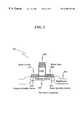
- an exemplary embodiment of the present invention( 300 ) consists simply of a conventional MOS gate stack ( 303 ) (gate electrode on silicon dioxide on a silicon substrate), metal source ( 301 ) and/or drain ( 302 ) electrodes, and channel dopants ( 304 ) that vary significantly in the vertical direction but not in the lateral direction.
- a field oxide ( 305 )electrically isolates devices from each other.
- the Schottky (or Schottky-like) barriers ( 307 , 308 ) that exist along the interface of the corresponding metal source/drain ( 301 , 302 ) and the silicon substrate ( 306 )act as an inherent pocket or halo implant and does so without added parasitic capacitance. It also eliminates the need for shallow source/drain extensions as the metal source/drain is by its nature shallow and highly conductive. Significant reductions in manufacturing complexity are therefore achieved by simultaneous elimination of the halo/pocket implants and the source/drain extensions. These are also major advantages over conventionally-architected-channel MOS devices.
- the metal source/drain(which replaces the conventional impurity doped source/drain) has a natural, very consistent and atomically abrupt Schottky barrier ( 307 , 308 ) with the silicon substrate ( 306 ) whose position and magnitude are independent of channel length, and because this barrier essentially plays the role of the halo/pocket implant (making these implants unnecessary), statistical variations due to random placement of atoms during the source/drain and halo/pocket implants are essentially eliminated. This fact remains true and even becomes more true as the channel length is reduced.
- the metal source/drain MOS architectureAnother benefit of the metal source/drain MOS architecture is the unconditional elimination of the parasitic bipolar gain.
- the parasitic bipolar gainis a direct result of using opposite doping types for the source/drain and substrate regions, and can result in latch-up and other deleterious effects.
- the source/drain electrodesare constructed of metal, this parasitic gain is eliminated. This makes the metal source/drain architecture ideal for (among other things) high-radiation environments.
- FIG. 1illustrates a prior art long channel, impurity doped source/drain device
- FIG. 2illustrates a prior art short channel, impurity doped source/drain device with pocket implants and source/drain extensions
- FIG. 3illustrates an exemplary embodiment of the present invention as applied to a short channel, metal source/drain device without pocket implants
- FIG. 4illustrates an exemplary embodiment of the present invention process fabrication step using an implanted silicon substrate with approximately 200 ⁇ screen oxide
- FIG. 5illustrates an exemplary embodiment of the present invention process fabrication step using a patterned in-situ doped silicon film on thin gate oxide
- FIG. 6illustrates an exemplary embodiment of the present invention process fabrication step using a formation of thin oxide sidewalls, and exposure of silicon in the gate, source and drain areas;
- FIG. 7illustrates an exemplary embodiment of the present invention process fabrication step using a metal deposition and silicidation anneal.
- FIG. 8illustrates an exemplary embodiment of the present invention process fabrication step using a removal of unreacted metal from the sidewalls
- FIG. 9illustrates an exemplary embodiment of the present invention process fabrication resulting structure.
- In-situ phosphorous doped silicon, Erbium silicide and Indium channel implantsare used for the N-type device for the gate electrode, source/drain electrodes and channel doping respectively.
- the P-type devicesmake use of in-situ Boron doped silicon, Platinum Silicide and Arsenic channel implants.
- the channel dopant concentrationsvary significantly in the vertical direction but not in the lateral direction. Gate lengths are typically ⁇ 100 nm, but may be longer;
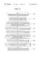
- FIG. 10illustrates an exemplary general system process flowchart showing a method of producing superior MOSFET devices
- FIG. 11illustrates an exemplary detailed system process flowchart showing a method of producing superior MOSFET devices.
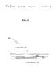
- the present inventionmay be aptly described in terms of exemplary system block diagrams and procedural flowcharts. While these items are sufficient to instruct one of ordinary skill in the art the teachings of the present invention, they should not be strictly construed as limiting the scope of the present invention.
- system block diagramsmay be combined and rearranged with no loss of generality, and procedural steps may be added or subtracted, and rearranged in order to achieve the same effect with no loss of teaching generality.
- the present invention as depicted in the attached exemplary system block diagrams and procedural flowchartsis for teaching purposes only and may be reworked by one skilled in the art depending on the intended target application.
- predetermined regionwill be defined to encompass the area centered at the heart of the active device (MOSFET).
- MOSFETactive device
- all the process steps mentioned in the context of a MOSFETwill create a gate, source/drain, and/or channel doping profiles as well as other structures in an area proximal to the predetermined regions or heart of the active device.
- the present inventionplaces no restrictions on what occurs outside this context, far from the heart of the active device.
- predetermined regionwill generally be spoken of in terms of a MOSFET device, this in no way limits the scope of the present invention.
- any device capable of regulating the flow of electrical currentmay be considered to have a predetermined region in proximity to its active current carrying region.
- the present inventionis particularly suitable for use with MOSFET semiconductor devices, but the use of the present teachings is not limited to this particular application.
- Other semiconductor devices, whether integrated or not,may be applied to the present invention teachings.
- this specificationspeaks in terms of ‘MOSFET’ devices, this term should be interpreted broadly to include any device for regulating the flow of electrical current having a conducting channel that has two or more points of electrical contact.
- the present inventionis particularly suitable for use in situations where short channel length MOSFETs are to be fabricated, especially in the range of channel lengths ⁇ 100nm.
- nothing in the teachings of the present inventionlimits application of the teachings of the present invention to these short channel length devices.
- Advantageous use of the teachings of the present inventionmay be had with channel lengths of any dimension.
- impurity atomsare selected from the group consisting of Arsenic, Phosphorous, Antimony, Boron, Indium, and/or Gallium as being within the scope of the teachings of the present invention.
- source and drainshould be interpreted to include the variants ‘drain’ and ‘source’ as well as ‘source or drain’ and ‘source and drain’.
- the present inventionspecifically anticipates that in some circumstances an interfacial layer may be utilized between the silicon substrate and the actual Schottky barrier metal.
- the present inventionspecifically anticipates ‘Schottky-like’ junctions and their equivalents to be useful in implementing the present invention.
- the interfacial layermay comprise materials that have conductive, semi-conductive, and/or insulator-like properties.
- This exemplary process flowis just exemplary of the broad teachings of the present invention, it will prove very instructive to one skilled in the art to teach the fundamental concepts of the present invention. This exemplary process flow may be described as follows:
- a thin screen oxide ( 401 )is grown (approximately 200 ⁇ ) to act as an implant mask.
- the appropriate channel dopant species ( 403 )for example Arsenic and Indium for P-type and N-type devices respectively
- the screen oxideis then removed in hydro-fluoric acid, and a thin gate oxide ( 501 ) (approximately 35 ⁇ ) is grown.
- the gate oxide growthis immediately followed by an in-situ doped silicon film.
- the filmis heavily doped with, for example, Phosphorous for an N-type device and Boron for a P-type device.
- the gate electrode ( 502 )is patterned as shown in the process step ( 500 ) illustrated in FIG. 5 .
- a thin oxide(approximately 100 ⁇ ) is then thermally grown on the top surface and sidewalls of the silicon gate electrode.
- an anisotropic etchis then used to remove the oxide layers on the horizontal surfaces (and thus expose the silicon ( 601 )), while preserving them on the vertical surfaces.
- a sidewall oxide ( 602 )is formed, and the dopants both in the gate electrode and in the channel region of the device are electrically activated as shown in the process step ( 600 ) illustrated in FIG. 6 .
- the final stepencompasses depositing an appropriate metal (for example, Platinum for the P-type device and Erbium for the N-type device) as a blanket film (approximately 400 ⁇ ) on all exposed surfaces.
- the waferis then annealed for a specified time at a specified temperature (for example, 400 ⁇ C for 45 minutes) so that, at all places where the metal is in direct contact with the silicon, a chemical reaction takes place that converts the metal to a metal silicide ( 701 ).
- the metal that was in direct contact with a non-silicon surface ( 702 )is left unaffected as shown in the process step ( 700 ) illustrated in FIG. 7 .
- a wet chemical etch(aqua regia for Platinum, HNO 3 for Erbium) is then used to remove the unreacted metal while leaving the metal-silicide untouched.
- the channel implanted, short channel Schottky barrier MOS deviceis now complete and ready for electrical contacting to gate, source, and drain as shown in the process step ( 800 ) illustrated in FIG. 8 .
- FIG. 9shows a preferred exemplary embodiment of the invention, as exemplified by two final complementary MOSFET structures ( 900 ).
- This embodimentconsists of N-channel devices fabricated with Erbium Silicide ( 904 ) for the source/drain regions, and a P-channel device fabricated with Platinum Silicide ( 905 ).
- Channel dopantsVertically varying, laterally non-varying Indium ( 902 ) and Arsenic ( 903 ) layers are used as the channel dopants for the N-channel and P-channel devices respectively. These dopant atoms are used due to their relatively low rates of diffusion through the silicon lattice (compared to Phosphorous and Boron, the other two possible candidates for channel dopants). This allows for greater thermal budget during fabrication of the device, and therefore less statistical variation in the characteristics of the finished product.
- the gate electrodesare fabricated from in-situ Phosphorous and Boron doped polysilicon films for the N-type ( 906 ) and P-type ( 907 ) devices respectively.
- Phosphorous and Boronare used due to their large solid-solubilities (compared to Arsenic and Indium).
- the electrodesare doped via the use of an in-situ method, wherein the impurity atoms are deposited at the same time the silicon atoms are. Such a method can achieve very large doping concentrations (approximately 10 21 /cm 3 ) and a uniform distribution throughout the thickness of the film.
- Another option for doping the silicon gateis ion-implantation. This method suffers from several practical problems including charging damage to the thin gate oxide, and the need to redistribute the highly non-uniform as-implanted gate dopants to achieve high doping levels at the gate oxide interface.
- the gate electrodes ( 906 ) and ( 907 )are less than 100 nm in width (corresponding to the channel length L), as it is in this regime that the advantages of the Schottky barrier architecture over the conventional architecture become apparent. These include simplified processing due to the absence of need for pocket implants, and the resulting reduction in yield loss, capacitance and statistical variations in finished products.
- Devicesare separated from each other by a thermally grown oxide (called a Field Oxide) ( 901 ) that works in conjunction with the channel dopants to electrically isolate the devices from each other.
- a Field Oxidea thermally grown oxide
- an exemplary generalized MOSFET device process fabrication flowstarts with a semiconductor substrate having means for electrically isolating transistors ( 1001 ). On this substrate, channel dopants are introduced in such a way that the dopant concentration varies significantly in the vertical but not the lateral direction ( 1002 ). Once this is complete, a gate electrode is formed ( 1003 ) on the silicon substrate. Finally, source and/or drain electrodes are formed, at least one of which incorporates a Schottky or Schottky-like contact to the semiconductor substrate ( 1004 ).
- an exemplary detailed MOSFET device process fabrication flowstarts with a semiconductor substrate having means for electrically isolating transistors ( 1101 ). On this substrate, channel dopants are introduced in such a way that the dopant concentration varies significantly in the vertical but not the lateral direction ( 1102 ). Once this is complete, a gate electrode insulator is formed by growing a thin gate insulating layer and depositing a conducting film ( 1103 ) on the silicon substrate.
- a series of pattern and etching stepsare performed to form a gate electrode ( 1104 ).
- one or more thin insulating layersare formed on one or more sidewalls of the gate electrode to selectively expose the semiconductor substrate on the active areas of the device except for the sidewalls ( 1105 ).
- a thin film of metalis deposited on all surfaces of the device ( 1106 ), and the device is thermally annealed to form a metal-semiconductor alloy on the exposed semiconductor surfaces ( 1107 ).
- unreacted metalis removed from the device while leaving the metal-semiconductor alloy untouched to form local interconnect for the formed device ( 1108 ).
- the present inventionmay be summarized by noting that the basic structure is one in which the substrate between the source and drain is uniformly doped in the lateral direction, non-uniformly doped in the vertical direction, and that the source and/or drain electrodes form Schottky or Schottky-like contacts with the substrate.
- a short channel length, laterally uniform doped channel, metal source and drain MOS device structure and method for manufacturehas been disclosed.
- the present inventionprovides for many advantages over the prior art including lower manufacturing costs, superior device characteristics, and tighter control of device parameters. These advantages are achieved primarily through the introduction of a channel doping profile that is both laterally uniform and vertically non-uniform, in conjunction with metal source/drain regions, thus eliminating the need for halo/pocket implants and shallow source/drain extensions. The parasitic bipolar gain is unconditionally eliminated as well.
Landscapes
- Insulated Gate Type Field-Effect Transistor (AREA)
- Electrodes Of Semiconductors (AREA)
- Thin Film Transistor (AREA)
- Metal-Oxide And Bipolar Metal-Oxide Semiconductor Integrated Circuits (AREA)
Abstract
Description
Claims (42)
Priority Applications (21)
| Application Number | Priority Date | Filing Date | Title |
|---|---|---|---|
| US09/465,357US6303479B1 (en) | 1999-12-16 | 1999-12-16 | Method of manufacturing a short-channel FET with Schottky-barrier source and drain contacts |
| AU22673/01AAU2267301A (en) | 1999-12-16 | 2000-12-15 | Mosfet device system and method |
| JP2001545358AJP2003517210A (en) | 1999-12-16 | 2000-12-15 | Systems and methods for MOSFET devices |
| IL15025000AIL150250A0 (en) | 1999-12-16 | 2000-12-15 | Mosfet device system and method |
| KR1020027007754AKR20020082469A (en) | 1999-12-16 | 2000-12-15 | Mosfet device system and method |
| EP00986434AEP1238420A4 (en) | 1999-12-16 | 2000-12-15 | MOSFET ARRANGEMENT, SYSTEM AND METHOD |
| PCT/US2000/034082WO2001045157A1 (en) | 1999-12-16 | 2000-12-15 | Mosfet device system and method |
| CA002393443ACA2393443A1 (en) | 1999-12-16 | 2000-12-15 | Mosfet device system and method |
| CNB008190194ACN1222021C (en) | 1999-12-16 | 2000-12-15 | MOSFET device systems and methods |
| RU2002118823/28ARU2245589C2 (en) | 1999-12-16 | 2000-12-15 | Mos-transistor and method of producing mos-transistor |
| US09/777,536US6495882B2 (en) | 1999-12-16 | 2001-02-06 | Short-channel schottky-barrier MOSFET device |
| IL150250AIL150250A (en) | 1999-12-16 | 2002-06-16 | Mosfet device system and method |
| US10/236,685US6744103B2 (en) | 1999-12-16 | 2002-09-06 | Short-channel schottky-barrier MOSFET device and manufacturing method |
| US10/360,194US7052945B2 (en) | 1999-12-16 | 2003-02-07 | Short-channel Schottky-barrier MOSFET device and manufacturing method |
| US10/440,472US20030235936A1 (en) | 1999-12-16 | 2003-05-16 | Schottky barrier CMOS device and method |
| US10/970,210US20050051815A1 (en) | 1999-12-16 | 2004-10-21 | Short-channel Schottky-barrier MOSFET device and manufacturing method |
| IL176106AIL176106A (en) | 1999-12-16 | 2006-06-04 | Mosfet device system |
| US11/478,478US7221019B2 (en) | 1999-12-16 | 2006-06-28 | Short-channel Schottky-barrier MOSFET device and manufacturing method |
| JP2006274467AJP2007049182A (en) | 1999-12-16 | 2006-10-05 | MOSFET device system and method |
| US12/581,097US20100032771A1 (en) | 1999-12-16 | 2009-10-16 | Short-channel schottky-barrier mosfet device and manufacturing method |
| US13/076,374US20110175160A1 (en) | 1999-12-16 | 2011-03-30 | Short-channel schottky-barrier mosfet device and method of manufacture |
Applications Claiming Priority (1)
| Application Number | Priority Date | Filing Date | Title |
|---|---|---|---|
| US09/465,357US6303479B1 (en) | 1999-12-16 | 1999-12-16 | Method of manufacturing a short-channel FET with Schottky-barrier source and drain contacts |
Related Child Applications (1)
| Application Number | Title | Priority Date | Filing Date |
|---|---|---|---|
| US09/777,536DivisionUS6495882B2 (en) | 1999-12-16 | 2001-02-06 | Short-channel schottky-barrier MOSFET device |
Publications (1)
| Publication Number | Publication Date |
|---|---|
| US6303479B1true US6303479B1 (en) | 2001-10-16 |
Family
ID=23847484
Family Applications (7)
| Application Number | Title | Priority Date | Filing Date |
|---|---|---|---|
| US09/465,357Expired - LifetimeUS6303479B1 (en) | 1999-12-16 | 1999-12-16 | Method of manufacturing a short-channel FET with Schottky-barrier source and drain contacts |
| US09/777,536Expired - Fee RelatedUS6495882B2 (en) | 1999-12-16 | 2001-02-06 | Short-channel schottky-barrier MOSFET device |
| US10/236,685Expired - LifetimeUS6744103B2 (en) | 1999-12-16 | 2002-09-06 | Short-channel schottky-barrier MOSFET device and manufacturing method |
| US10/360,194Expired - LifetimeUS7052945B2 (en) | 1999-12-16 | 2003-02-07 | Short-channel Schottky-barrier MOSFET device and manufacturing method |
| US10/970,210AbandonedUS20050051815A1 (en) | 1999-12-16 | 2004-10-21 | Short-channel Schottky-barrier MOSFET device and manufacturing method |
| US12/581,097AbandonedUS20100032771A1 (en) | 1999-12-16 | 2009-10-16 | Short-channel schottky-barrier mosfet device and manufacturing method |
| US13/076,374AbandonedUS20110175160A1 (en) | 1999-12-16 | 2011-03-30 | Short-channel schottky-barrier mosfet device and method of manufacture |
Family Applications After (6)
| Application Number | Title | Priority Date | Filing Date |
|---|---|---|---|
| US09/777,536Expired - Fee RelatedUS6495882B2 (en) | 1999-12-16 | 2001-02-06 | Short-channel schottky-barrier MOSFET device |
| US10/236,685Expired - LifetimeUS6744103B2 (en) | 1999-12-16 | 2002-09-06 | Short-channel schottky-barrier MOSFET device and manufacturing method |
| US10/360,194Expired - LifetimeUS7052945B2 (en) | 1999-12-16 | 2003-02-07 | Short-channel Schottky-barrier MOSFET device and manufacturing method |
| US10/970,210AbandonedUS20050051815A1 (en) | 1999-12-16 | 2004-10-21 | Short-channel Schottky-barrier MOSFET device and manufacturing method |
| US12/581,097AbandonedUS20100032771A1 (en) | 1999-12-16 | 2009-10-16 | Short-channel schottky-barrier mosfet device and manufacturing method |
| US13/076,374AbandonedUS20110175160A1 (en) | 1999-12-16 | 2011-03-30 | Short-channel schottky-barrier mosfet device and method of manufacture |
Country Status (10)
| Country | Link |
|---|---|
| US (7) | US6303479B1 (en) |
| EP (1) | EP1238420A4 (en) |
| JP (2) | JP2003517210A (en) |
| KR (1) | KR20020082469A (en) |
| CN (1) | CN1222021C (en) |
| AU (1) | AU2267301A (en) |
| CA (1) | CA2393443A1 (en) |
| IL (3) | IL150250A0 (en) |
| RU (1) | RU2245589C2 (en) |
| WO (1) | WO2001045157A1 (en) |
Cited By (64)
| Publication number | Priority date | Publication date | Assignee | Title |
|---|---|---|---|---|
| US20020011613A1 (en)* | 2000-07-11 | 2002-01-31 | Kabushiki Kaisha Toshiba | Semiconductor device and method for manufacturing the same |
| US6466489B1 (en)* | 2001-05-18 | 2002-10-15 | International Business Machines Corporation | Use of source/drain asymmetry MOSFET devices in dynamic and analog circuits |
| US20030008444A1 (en)* | 1999-12-16 | 2003-01-09 | Snyder John P. | Short-channel schottky-barrier MOSFET device and manufacturing method |
| US20030034532A1 (en)* | 2001-08-10 | 2003-02-20 | Snyder John P. | Transistor having high dielectric constant gate insulating layer and source and drain forming schottky contact with substrate |
| US6531381B2 (en)* | 2001-05-25 | 2003-03-11 | Mitsubishi Denki Kabushiki Kaisha | Method and apparatus for cleaning semiconductor device and method of fabricating semiconductor device |
| US6534388B1 (en)* | 2000-09-27 | 2003-03-18 | Chartered Semiconductor Manufacturing Ltd. | Method to reduce variation in LDD series resistance |
| US6541320B2 (en)* | 2001-08-10 | 2003-04-01 | International Business Machines Corporation | Method to controllably form notched polysilicon gate structures |
| US6555453B1 (en)* | 2001-01-31 | 2003-04-29 | Advanced Micro Devices, Inc. | Fully nickel silicided metal gate with shallow junction formed |
| US20030139001A1 (en)* | 2002-01-23 | 2003-07-24 | Snyder John P. | Field effect transistor having source and/or drain forming schottky or schottky-like contact with strained semiconductor substrate |
| US20030235936A1 (en)* | 1999-12-16 | 2003-12-25 | Snyder John P. | Schottky barrier CMOS device and method |
| US20040026687A1 (en)* | 2002-08-12 | 2004-02-12 | Grupp Daniel E. | Method for depinning the fermi level of a semiconductor at an electrical junction and devices incorporating such junctions |
| US20040041226A1 (en)* | 2002-05-16 | 2004-03-04 | Snyder John P. | Schottky barrier CMOS device and method |
| US20040041176A1 (en)* | 2002-08-29 | 2004-03-04 | Prall Kirk D. | One F2 memory cell, memory array, related devices and methods |
| US6744111B1 (en) | 2003-05-15 | 2004-06-01 | Koucheng Wu | Schottky-barrier tunneling transistor |
| US20040130934A1 (en)* | 2002-06-21 | 2004-07-08 | Micron Technology, Inc. | NROM memory cell, memory array, related devices and methods |
| US6791140B2 (en) | 2002-08-08 | 2004-09-14 | Micron Technology, Inc. | Memory transistor structure |
| US20040206980A1 (en)* | 2003-04-16 | 2004-10-21 | Cheong Woo Seok | Schottky barrier transistor and method of manufacturing the same |
| US20040227203A1 (en)* | 2003-05-15 | 2004-11-18 | Koucheng Wu | Schottky-barrier tunneling transistor |
| US20050012087A1 (en)* | 2003-07-15 | 2005-01-20 | Yi-Ming Sheu | Self-aligned MOSFET having an oxide region below the channel |
| US20050035410A1 (en)* | 2003-08-15 | 2005-02-17 | Yee-Chia Yeo | Semiconductor diode with reduced leakage |
| US20050035369A1 (en)* | 2003-08-15 | 2005-02-17 | Chun-Chieh Lin | Structure and method of forming integrated circuits utilizing strained channel transistors |
| US20050035470A1 (en)* | 2003-08-12 | 2005-02-17 | Chih-Hsin Ko | Strained channel complementary field-effect transistors and methods of manufacture |
| US20050093067A1 (en)* | 2003-04-30 | 2005-05-05 | Yee-Chia Yeo | Semiconductor-on-insulator chip incorporating strained-channel partially-depleted, fully-depleted, and multiple-gate transistors |
| US20050093027A1 (en)* | 2002-08-12 | 2005-05-05 | Grupp Daniel E. | Method for depinning the fermi level of a semiconductor at an electrical junction and devices incorporating such junctions |
| US6894355B1 (en)* | 2002-01-11 | 2005-05-17 | Advanced Micro Devices, Inc. | Semiconductor device with silicide source/drain and high-K dielectric |
| US20050118793A1 (en)* | 2003-10-03 | 2005-06-02 | Snyder John P. | Schottky-barrier MOSFET manufacturing method using isotropic etch process |
| US20050128804A1 (en)* | 2003-12-16 | 2005-06-16 | Micron Technology, Inc. | Multi-state NROM device |
| US20050139860A1 (en)* | 2003-10-22 | 2005-06-30 | Snyder John P. | Dynamic schottky barrier MOSFET device and method of manufacture |
| US20050208717A1 (en)* | 2003-07-25 | 2005-09-22 | Yee-Chia Yeo | Capacitor with enhanced performance and method of manufacture |
| US20050275033A1 (en)* | 2004-05-11 | 2005-12-15 | Shiyang Zhu | Schottky barrier source/drain N-MOSFET using ytterbium silicide |
| US20060079059A1 (en)* | 2001-08-10 | 2006-04-13 | Snyder John P | Transistor having high dielectric constant gate insulating layer and source and drain forming schottky contact with substrate |
| US20060084232A1 (en)* | 2002-08-12 | 2006-04-20 | Grupp Daniel E | Process for fabricating a self-aligned deposited source/drain insulated gate field-effect transistor |
| US20060124992A1 (en)* | 2003-12-16 | 2006-06-15 | Micron Technology, Inc. | NROM memory cell, memory array, related devices and methods |
| US20060125041A1 (en)* | 2004-12-14 | 2006-06-15 | Electronics And Telecommunications Research Institute | Transistor using impact ionization and method of manufacturing the same |
| US20060131621A1 (en)* | 2004-12-21 | 2006-06-22 | Shin Jae H | Device using ambipolar transport in SB-MOSFET and method for operating the same |
| US20060141728A1 (en)* | 2003-06-03 | 2006-06-29 | Koninklijke Philips Electronics N.V. | Formation of junctions and silicides with reduced thermal budget |
| US20060226487A1 (en)* | 2003-08-18 | 2006-10-12 | Yee-Chia Yeo | Resistor with reduced leakage |
| US20070026597A1 (en)* | 2005-07-29 | 2007-02-01 | Kazuaki Nakajima | Method of manufacturing semiconductor device |
| US20070026591A1 (en)* | 2002-08-12 | 2007-02-01 | Grupp Daniel E | Insulated gate field effect transistor having passivated schottky barriers to the channel |
| US20070080406A1 (en)* | 2005-10-12 | 2007-04-12 | Spinnaker Semiconductor, Inc. | CMOS device with zero soft error rate |
| US20070111435A1 (en)* | 2005-11-14 | 2007-05-17 | Sumsung Electronics Co., Ltd. | Schottky barrier finfet device and fabrication method thereof |
| US20070187756A1 (en)* | 2004-07-15 | 2007-08-16 | Snyder John P | Metal Source Power Transistor And Method Of Manufacture |
| US20080093631A1 (en)* | 2006-10-05 | 2008-04-24 | Chi Dong Z | Contact structure for semiconductor devices |
| US20080191285A1 (en)* | 2007-02-09 | 2008-08-14 | Chih-Hsin Ko | CMOS devices with schottky source and drain regions |
| CN100423198C (en)* | 2001-11-22 | 2008-10-01 | 韩国电子通信研究院 | Method for fabricating MOS transistors with shallow source/drain junction regions |
| US20080274601A1 (en)* | 2007-05-04 | 2008-11-06 | Min Byoung W | Method of forming a transistor having multiple types of schottky junctions |
| US7646068B2 (en) | 2003-08-15 | 2010-01-12 | Taiwan Semiconductor Manufacturing Company, Ltd. | Structure and method of a strained channel transistor and a second semiconductor component in an integrated circuit |
| US20100102298A1 (en)* | 2008-10-26 | 2010-04-29 | Koucheng Wu | Schottky barrier quantum well resonant tunneling transistor |
| US7745279B2 (en) | 2003-07-25 | 2010-06-29 | Taiwan Semiconductor Manufacturing Company, Ltd. | Capacitor that includes high permittivity capacitor dielectric |
| US7808051B2 (en) | 2008-09-29 | 2010-10-05 | Taiwan Semiconductor Manufacturing Company, Ltd. | Standard cell without OD space effect in Y-direction |
| US20100320510A1 (en)* | 2009-06-21 | 2010-12-23 | International Sematech | Interfacial Barrier for Work Function Modification of High Performance CMOS Devices |
| US7867860B2 (en) | 2003-07-25 | 2011-01-11 | Taiwan Semiconductor Manufacturing Company, Ltd. | Strained channel transistor formation |
| US7888201B2 (en) | 2003-11-04 | 2011-02-15 | Taiwan Semiconductor Manufacturing Company, Ltd. | Semiconductor-on-insulator SRAM configured using partially-depleted and fully-depleted transistors |
| US7943961B2 (en) | 2008-03-13 | 2011-05-17 | Taiwan Semiconductor Manufacturing Company, Ltd. | Strain bars in stressed layers of MOS devices |
| US20120104502A1 (en)* | 2009-03-31 | 2012-05-03 | Jx Nippon Mining & Metals Corporation | Method of producing semiconductor device, and semiconductor device |
| US8436422B2 (en) | 2010-03-08 | 2013-05-07 | Sematech, Inc. | Tunneling field-effect transistor with direct tunneling for enhanced tunneling current |
| US8558278B2 (en) | 2007-01-16 | 2013-10-15 | Taiwan Semiconductor Manufacturing Company, Ltd. | Strained transistor with optimized drive current and method of forming |
| US9620611B1 (en) | 2016-06-17 | 2017-04-11 | Acorn Technology, Inc. | MIS contact structure with metal oxide conductor |
| US20180308959A1 (en)* | 2017-04-20 | 2018-10-25 | Taiwan Semiconductor Manufacturing Co., Ltd. | Semiconductor device and method of manufacturing the same |
| US10170627B2 (en) | 2016-11-18 | 2019-01-01 | Acorn Technologies, Inc. | Nanowire transistor with source and drain induced by electrical contacts with negative schottky barrier height |
| RU2743225C1 (en)* | 2020-09-14 | 2021-02-16 | Акционерное общество "Научно-производственное предприятие "Исток" имени А.И. Шокина" (АО "НПП "Исток" им. Шокина") | Field-effect transistor with schottky barrier |
| WO2021092117A1 (en) | 2019-11-06 | 2021-05-14 | Silicet, LLC | Devices and methods for ldmos and other mos transistors with hybrid contact |
| US11228174B1 (en) | 2019-05-30 | 2022-01-18 | Silicet, LLC | Source and drain enabled conduction triggers and immunity tolerance for integrated circuits |
| US11522053B2 (en) | 2020-12-04 | 2022-12-06 | Amplexia, Llc | LDMOS with self-aligned body and hybrid source |
Families Citing this family (70)
| Publication number | Priority date | Publication date | Assignee | Title |
|---|---|---|---|---|
| FR2805395B1 (en)* | 2000-02-23 | 2002-05-10 | Centre Nat Rech Scient | MOS TRANSISTOR FOR HIGH INTEGRATION DENSITY CIRCUITS |
| DE10052208C2 (en)* | 2000-10-20 | 2002-11-28 | Advanced Micro Devices Inc | Method for producing a field effect transistor using an adjustment technology based on side wall spacing elements |
| DE10137217A1 (en)* | 2001-07-30 | 2003-02-27 | Infineon Technologies Ag | Bridge field effect transistor and method for producing a bridge field effect transistor |
| DE10208728B4 (en)* | 2002-02-28 | 2009-05-07 | Advanced Micro Devices, Inc., Sunnyvale | A method for producing a semiconductor element having different metal silicide regions |
| JP2006514424A (en)* | 2002-05-16 | 2006-04-27 | スピネカ セミコンダクター, インコーポレイテッド | Schottky barrier CMOS device and method |
| US7208383B1 (en) | 2002-10-30 | 2007-04-24 | Advanced Micro Devices, Inc. | Method of manufacturing a semiconductor component |
| US6833307B1 (en) | 2002-10-30 | 2004-12-21 | Advanced Micro Devices, Inc. | Method for manufacturing a semiconductor component having an early halo implant |
| US20040087094A1 (en)* | 2002-10-30 | 2004-05-06 | Advanced Micro Devices, Inc. | Semiconductor component and method of manufacture |
| EP1435648A1 (en)* | 2002-12-30 | 2004-07-07 | STMicroelectronics S.r.l. | Process of making CMOS and drain extension MOS transistors with silicided gate |
| US6909151B2 (en)* | 2003-06-27 | 2005-06-21 | Intel Corporation | Nonplanar device with stress incorporation layer and method of fabrication |
| US7456476B2 (en) | 2003-06-27 | 2008-11-25 | Intel Corporation | Nonplanar semiconductor device with partially or fully wrapped around gate electrode and methods of fabrication |
| US20050104152A1 (en)* | 2003-09-19 | 2005-05-19 | Snyder John P. | Schottky barrier integrated circuit |
| JP4011024B2 (en)* | 2004-01-30 | 2007-11-21 | 株式会社ルネサステクノロジ | Semiconductor device and manufacturing method thereof |
| US7154118B2 (en) | 2004-03-31 | 2006-12-26 | Intel Corporation | Bulk non-planar transistor having strained enhanced mobility and methods of fabrication |
| US7579280B2 (en) | 2004-06-01 | 2009-08-25 | Intel Corporation | Method of patterning a film |
| US7042009B2 (en)* | 2004-06-30 | 2006-05-09 | Intel Corporation | High mobility tri-gate devices and methods of fabrication |
| US7348284B2 (en) | 2004-08-10 | 2008-03-25 | Intel Corporation | Non-planar pMOS structure with a strained channel region and an integrated strained CMOS flow |
| US7422946B2 (en) | 2004-09-29 | 2008-09-09 | Intel Corporation | Independently accessed double-gate and tri-gate transistors in same process flow |
| US7332439B2 (en)* | 2004-09-29 | 2008-02-19 | Intel Corporation | Metal gate transistors with epitaxial source and drain regions |
| US7361958B2 (en) | 2004-09-30 | 2008-04-22 | Intel Corporation | Nonplanar transistors with metal gate electrodes |
| US20060086977A1 (en) | 2004-10-25 | 2006-04-27 | Uday Shah | Nonplanar device with thinned lower body portion and method of fabrication |
| JP2006196646A (en)* | 2005-01-13 | 2006-07-27 | Renesas Technology Corp | Semiconductor device and manufacturing method thereof |
| US7518196B2 (en) | 2005-02-23 | 2009-04-14 | Intel Corporation | Field effect transistor with narrow bandgap source and drain regions and method of fabrication |
| US20060202266A1 (en) | 2005-03-14 | 2006-09-14 | Marko Radosavljevic | Field effect transistor with metal source/drain regions |
| JP2008226862A (en)* | 2005-05-11 | 2008-09-25 | Interuniv Micro Electronica Centrum Vzw | Method for adjusting the work function of a silicided gate electrode |
| US7504329B2 (en)* | 2005-05-11 | 2009-03-17 | Interuniversitair Microelektronica Centrum (Imec) | Method of forming a Yb-doped Ni full silicidation low work function gate electrode for n-MOSFET |
| US7176537B2 (en) | 2005-05-23 | 2007-02-13 | Taiwan Semiconductor Manufacturing Company, Ltd. | High performance CMOS with metal-gate and Schottky source/drain |
| US7858481B2 (en) | 2005-06-15 | 2010-12-28 | Intel Corporation | Method for fabricating transistor with thinned channel |
| US7547637B2 (en) | 2005-06-21 | 2009-06-16 | Intel Corporation | Methods for patterning a semiconductor film |
| US7279375B2 (en) | 2005-06-30 | 2007-10-09 | Intel Corporation | Block contact architectures for nanoscale channel transistors |
| US7402875B2 (en) | 2005-08-17 | 2008-07-22 | Intel Corporation | Lateral undercut of metal gate in SOI device |
| US7737532B2 (en)* | 2005-09-06 | 2010-06-15 | Taiwan Semiconductor Manufacturing Company, Ltd. | Hybrid Schottky source-drain CMOS for high mobility and low barrier |
| US7479421B2 (en) | 2005-09-28 | 2009-01-20 | Intel Corporation | Process for integrating planar and non-planar CMOS transistors on a bulk substrate and article made thereby |
| US20070090416A1 (en) | 2005-09-28 | 2007-04-26 | Doyle Brian S | CMOS devices with a single work function gate electrode and method of fabrication |
| US7250666B2 (en)* | 2005-11-15 | 2007-07-31 | International Business Machines Corporation | Schottky barrier diode and method of forming a Schottky barrier diode |
| US7485503B2 (en) | 2005-11-30 | 2009-02-03 | Intel Corporation | Dielectric interface for group III-V semiconductor device |
| KR100699462B1 (en)* | 2005-12-07 | 2007-03-28 | 한국전자통신연구원 | Schottky Barrier Through Transistors and Manufacturing Method Thereof |
| JP2007158300A (en)* | 2005-12-07 | 2007-06-21 | Korea Electronics Telecommun | Low Schottky barrier through transistor and method of manufacturing the same |
| US7396711B2 (en)* | 2005-12-27 | 2008-07-08 | Intel Corporation | Method of fabricating a multi-cornered film |
| FR2897202B1 (en)* | 2006-02-08 | 2008-09-12 | St Microelectronics Crolles 2 | MOS TRANSISTOR WITH SCHOTTKY BARRIER ON SEMICONDUCTOR FILM ENTIRELY DEPLETED AND METHOD OF MANUFACTURING SUCH TRANSISTOR |
| JP2007281038A (en)* | 2006-04-03 | 2007-10-25 | Toshiba Corp | Semiconductor device |
| US7566951B2 (en)* | 2006-04-21 | 2009-07-28 | Memc Electronic Materials, Inc. | Silicon structures with improved resistance to radiation events |
| US8143646B2 (en) | 2006-08-02 | 2012-03-27 | Intel Corporation | Stacking fault and twin blocking barrier for integrating III-V on Si |
| KR100770012B1 (en)* | 2006-11-29 | 2007-10-25 | 한국전자통신연구원 | Schottky Barrier Through Transistors and Manufacturing Method Thereof |
| KR100945508B1 (en)* | 2007-11-16 | 2010-03-09 | 주식회사 하이닉스반도체 | Zero Capacitor Ram and Method of Manufacturing the Same |
| FR2930073B1 (en)* | 2008-04-11 | 2010-09-03 | Centre Nat Rech Scient | METHOD FOR MANUFACTURING COMPLEMENTARY P AND N TYPE MOSFET TRANSISTORS, AND ELECTRONIC DEVICE COMPRISING SUCH TRANSISTORS, AND PROCESSOR COMPRISING AT LEAST ONE SUCH DEVICE. |
| US7863143B2 (en)* | 2008-05-01 | 2011-01-04 | International Business Machines Corporation | High performance schottky-barrier-source asymmetric MOSFETs |
| US8362566B2 (en) | 2008-06-23 | 2013-01-29 | Intel Corporation | Stress in trigate devices using complimentary gate fill materials |
| JP4911158B2 (en)* | 2008-10-30 | 2012-04-04 | ソニー株式会社 | Semiconductor device and solid-state imaging device |
| US9054194B2 (en) | 2009-04-29 | 2015-06-09 | Taiwan Semiconductor Manufactruing Company, Ltd. | Non-planar transistors and methods of fabrication thereof |
| CN102598284B (en)* | 2009-11-06 | 2015-04-15 | 株式会社半导体能源研究所 | Semiconductor device |
| CN101866953B (en)* | 2010-05-26 | 2012-08-22 | 清华大学 | Low Schottky barrier semiconductor structure and formation method thereof |
| US8513765B2 (en) | 2010-07-19 | 2013-08-20 | International Business Machines Corporation | Formation method and structure for a well-controlled metallic source/drain semiconductor device |
| RU2431905C1 (en)* | 2010-07-23 | 2011-10-20 | Открытое Акционерное Общество "Воронежский Завод Полупроводниковых Приборов-Сборка" | Method for manufacturing of semiconductor device |
| US8957462B2 (en)* | 2010-12-09 | 2015-02-17 | Semiconductor Energy Laboratory Co., Ltd. | Semiconductor device comprising an N-type transistor with an N-type semiconductor containing nitrogen as a gate |
| US8610233B2 (en) | 2011-03-16 | 2013-12-17 | International Business Machines Corporation | Hybrid MOSFET structure having drain side schottky junction |
| US9001564B2 (en) | 2011-06-29 | 2015-04-07 | Semiconductor Energy Laboratory Co., Ltd. | Semiconductor device and a method for driving the same |
| US8797512B2 (en)* | 2011-09-15 | 2014-08-05 | Advanced Scientific Concepts, Inc. | Automatic range corrected flash ladar camera |
| US8803242B2 (en)* | 2011-09-19 | 2014-08-12 | Eta Semiconductor Inc. | High mobility enhancement mode FET |
| CN102446770A (en)* | 2011-10-12 | 2012-05-09 | 上海华力微电子有限公司 | Method and structure for improving writing speed of floating body dynamic random access memory unit |
| CN102723367B (en)* | 2012-06-29 | 2015-02-11 | 昆山工研院新型平板显示技术中心有限公司 | Oxide semiconductor thin film transistor |
| US9576949B2 (en)* | 2012-09-05 | 2017-02-21 | Taiwan Semiconductor Manufacturing Company, Ltd. | Diode formed of PMOSFET and schottky diodes |
| DE102012215846A1 (en)* | 2012-09-06 | 2014-03-06 | Continental Automotive Gmbh | Battery arrangement for operating electrical consumers in a vehicle for transporting dangerous goods |
| US8796098B1 (en)* | 2013-02-26 | 2014-08-05 | Cypress Semiconductor Corporation | Embedded SONOS based memory cells |
| US9059156B2 (en)* | 2013-09-30 | 2015-06-16 | Intermolecular, Inc. | Method of forming an erbium silicide metal gate stack FinFET device via a physical vapor deposition nanolaminate approach |
| KR102236555B1 (en) | 2014-11-11 | 2021-04-06 | 삼성전자주식회사 | Semiconductor devices and methods of manufacturing the same |
| US10510869B2 (en) | 2016-05-06 | 2019-12-17 | Silicet, LLC | Devices and methods for a power transistor having a Schottky or Schottky-like contact |
| US9947787B2 (en) | 2016-05-06 | 2018-04-17 | Silicet, LLC | Devices and methods for a power transistor having a schottky or schottky-like contact |
| RU2752291C2 (en)* | 2018-01-17 | 2021-07-26 | Интел Корпорейшн | Apparatuses based on selectively epitaxially grown iii-v group materials |
| US11417762B2 (en)* | 2019-06-26 | 2022-08-16 | Skyworks Solutions, Inc. | Switch with integrated Schottky barrier contact |
Citations (11)
| Publication number | Priority date | Publication date | Assignee | Title |
|---|---|---|---|---|
| US4053924A (en) | 1975-02-07 | 1977-10-11 | California Linear Circuits, Inc. | Ion-implanted semiconductor abrupt junction |
| US4300152A (en)* | 1980-04-07 | 1981-11-10 | Bell Telephone Laboratories, Incorporated | Complementary field-effect transistor integrated circuit device |
| US4485550A (en)* | 1982-07-23 | 1984-12-04 | At&T Bell Laboratories | Fabrication of schottky-barrier MOS FETs |
| US4942441A (en)* | 1986-03-29 | 1990-07-17 | Hitachi, Ltd. | Thin film semiconductor device and method of manufacturing the same |
| US5079182A (en) | 1990-04-02 | 1992-01-07 | National Semiconductor Corporation | Bicmos device having self-aligned well tap and method of fabrication |
| EP0603102A2 (en)* | 1992-12-18 | 1994-06-22 | International Business Machines Corporation | Low-temperature MOSFET source drain structure with ultra-short channel |
| US5444302A (en) | 1992-12-25 | 1995-08-22 | Hitachi, Ltd. | Semiconductor device including multi-layer conductive thin film of polycrystalline material |
| US5663584A (en)* | 1994-05-31 | 1997-09-02 | Welch; James D. | Schottky barrier MOSFET systems and fabrication thereof |
| US5767557A (en) | 1994-12-01 | 1998-06-16 | Lucent Technologies Inc. | PMOSFETS having indium or gallium doped buried channels and n+polysilicon gates and CMOS devices fabricated therefrom |
| US5801398A (en) | 1994-10-18 | 1998-09-01 | Frontec Corporation | Field effect transistor |
| US6037605A (en) | 1996-08-20 | 2000-03-14 | Kabushiki Kaisha Toshiba | Semiconductor device and method of manufacturing the same |
Family Cites Families (47)
| Publication number | Priority date | Publication date | Assignee | Title |
|---|---|---|---|---|
| US4300158A (en) | 1977-07-18 | 1981-11-10 | Hazeltine Corporation | Process control apparatus |
| USRE32613E (en)* | 1980-04-17 | 1988-02-23 | American Telephone And Telegraph Company, At&T Bell Laboratories | Method of making contact electrodes to silicon gate, and source and drain regions, of a semiconductor device |
| SE8101994L (en)* | 1981-03-27 | 1982-09-28 | Tove Per Arne | ELECTRONIC CIRCUIT WITH SCHOTTKY FIELD TRANSISTOR WITH CONTACT ELEMENT WITH DIFFERENT SCHOTTKY BARRIER HEAD |
| JPS5947767A (en)* | 1982-09-10 | 1984-03-17 | Nippon Telegr & Teleph Corp <Ntt> | MIS type semiconductor device |
| US4513309A (en)* | 1982-11-03 | 1985-04-23 | Westinghouse Electric Corp. | Prevention of latch-up in CMOS integrated circuits using Schottky diodes |
| JPH0810763B2 (en)* | 1983-12-28 | 1996-01-31 | 株式会社日立製作所 | Semiconductor device |
| EP0191841A1 (en)* | 1984-08-24 | 1986-08-27 | AT&T Corp. | Mos transistors having schottky layer electrode regions and method of their production |
| JPS6099553U (en)* | 1984-10-25 | 1985-07-06 | 富士通株式会社 | semiconductor equipment |
| FR2582445B1 (en)* | 1985-05-21 | 1988-04-08 | Efcis | METHOD FOR MANUFACTURING METAL SILICIDE ELECTRODE MOS TRANSISTORS |
| US5834793A (en)* | 1985-12-27 | 1998-11-10 | Kabushiki Kaisha Toshiba | Semiconductor devices |
| JPH02188967A (en)* | 1989-01-18 | 1990-07-25 | Nissan Motor Co Ltd | Semiconductor device |
| DE4001350C2 (en)* | 1989-01-18 | 1993-10-07 | Nissan Motor | Semiconductor device |
| JP2606404B2 (en)* | 1990-04-06 | 1997-05-07 | 日産自動車株式会社 | Semiconductor device |
| US5369295A (en)* | 1992-01-28 | 1994-11-29 | Thunderbird Technologies, Inc. | Fermi threshold field effect transistor with reduced gate and diffusion capacitance |
| US5289030A (en) | 1991-03-06 | 1994-02-22 | Semiconductor Energy Laboratory Co., Ltd. | Semiconductor device with oxide layer |
| US5250834A (en)* | 1991-09-19 | 1993-10-05 | International Business Machines Corporation | Silicide interconnection with schottky barrier diode isolation |
| JP3118063B2 (en)* | 1992-03-23 | 2000-12-18 | ローム株式会社 | Nonvolatile storage element, nonvolatile storage device using the same, and method of manufacturing nonvolatile storage element |
| US5323053A (en)* | 1992-05-28 | 1994-06-21 | At&T Bell Laboratories | Semiconductor devices using epitaxial silicides on (111) surfaces etched in (100) silicon substrates |
| US5294814A (en)* | 1992-06-09 | 1994-03-15 | Kobe Steel Usa | Vertical diamond field effect transistor |
| JPH0697109A (en) | 1992-09-16 | 1994-04-08 | Fujitsu Ltd | Semiconductor device |
| US5323528A (en)* | 1993-06-14 | 1994-06-28 | Amistar Corporation | Surface mount placement system |
| US5760449A (en)* | 1994-05-31 | 1998-06-02 | Welch; James D. | Regenerative switching CMOS system |
| US6268636B1 (en)* | 1994-05-31 | 2001-07-31 | James D. Welch | Operation and biasing for single device equivalent to CMOS |
| US5665993A (en)* | 1994-09-29 | 1997-09-09 | Texas Instruments Incorporated | Integrated circuit including a FET device and Schottky diode |
| US5555993A (en)* | 1995-02-24 | 1996-09-17 | Borkowski; James T. | Beverage can and pivotal, screen guard opener system |
| FR2749977B1 (en)* | 1996-06-14 | 1998-10-09 | Commissariat Energie Atomique | QUANTUM WELL MOS TRANSISTOR AND METHODS OF MANUFACTURE THEREOF |
| US5882993A (en)* | 1996-08-19 | 1999-03-16 | Advanced Micro Devices, Inc. | Integrated circuit with differing gate oxide thickness and process for making same |
| JP3262752B2 (en)* | 1997-03-28 | 2002-03-04 | 松下電器産業株式会社 | Method for manufacturing semiconductor device |
| US5883010A (en)* | 1997-08-07 | 1999-03-16 | National Semiconductor Corporation | Method for protecting nonsilicided surfaces from silicide formation using spacer oxide mask |
| US5952701A (en)* | 1997-08-18 | 1999-09-14 | National Semiconductor Corporation | Design and fabrication of semiconductor structure having complementary channel-junction insulated-gate field-effect transistors whose gate electrodes have work functions close to mid-gap semiconductor value |
| JP4213776B2 (en)* | 1997-11-28 | 2009-01-21 | 光照 木村 | MOS gate Schottky tunnel transistor and integrated circuit using the same |
| US6160282A (en)* | 1998-04-21 | 2000-12-12 | Foveon, Inc. | CMOS image sensor employing silicide exclusion mask to reduce leakage and improve performance |
| JP3378512B2 (en) | 1998-10-16 | 2003-02-17 | 株式会社東芝 | Semiconductor device |
| JP3408762B2 (en)* | 1998-12-03 | 2003-05-19 | シャープ株式会社 | Semiconductor device having SOI structure and method of manufacturing the same |
| US6949787B2 (en)* | 2001-08-10 | 2005-09-27 | Spinnaker Semiconductor, Inc. | Transistor having high dielectric constant gate insulating layer and source and drain forming Schottky contact with substrate |
| US20030032270A1 (en)* | 2001-08-10 | 2003-02-13 | John Snyder | Fabrication method for a device for regulating flow of electric current with high dielectric constant gate insulating layer and source/drain forming schottky contact or schottky-like region with substrate |
| US6303479B1 (en) | 1999-12-16 | 2001-10-16 | Spinnaker Semiconductor, Inc. | Method of manufacturing a short-channel FET with Schottky-barrier source and drain contacts |
| US20030235936A1 (en)* | 1999-12-16 | 2003-12-25 | Snyder John P. | Schottky barrier CMOS device and method |
| JP3675303B2 (en)* | 2000-05-31 | 2005-07-27 | セイコーエプソン株式会社 | Semiconductor device with built-in electrostatic protection circuit and manufacturing method thereof |
| KR100439398B1 (en)* | 2001-05-22 | 2004-07-09 | 주식회사 멀티채널랩스 | Digital controlled electronic ballast with piezoelectric transformer |
| US6509609B1 (en)* | 2001-06-18 | 2003-01-21 | Motorola, Inc. | Grooved channel schottky MOSFET |
| JP2005516389A (en)* | 2002-01-23 | 2005-06-02 | スピネカ セミコンダクター, インコーポレイテッド | Field effect transistor having a source and / or drain forming a Schottky or Schottky contact using a strained semiconductor substrate |
| US6974737B2 (en)* | 2002-05-16 | 2005-12-13 | Spinnaker Semiconductor, Inc. | Schottky barrier CMOS fabrication method |
| US6833556B2 (en)* | 2002-08-12 | 2004-12-21 | Acorn Technologies, Inc. | Insulated gate field effect transistor having passivated schottky barriers to the channel |
| JP4439358B2 (en)* | 2003-09-05 | 2010-03-24 | 株式会社東芝 | Field effect transistor and manufacturing method thereof |
| RU2006114833A (en)* | 2003-10-03 | 2007-11-10 | Спиннэйкер Семикондактор, Инк. (Us) | METHOD FOR PRODUCING A MOSFET FIELD TRANSISTOR WITH A SCHOTKI BARRIER USING THE ISOTROPIC ETCHING PROCESS |
| US20050139860A1 (en)* | 2003-10-22 | 2005-06-30 | Snyder John P. | Dynamic schottky barrier MOSFET device and method of manufacture |
- 1999
- 1999-12-16USUS09/465,357patent/US6303479B1/ennot_activeExpired - Lifetime
- 2000
- 2000-12-15EPEP00986434Apatent/EP1238420A4/ennot_activeWithdrawn
- 2000-12-15ILIL15025000Apatent/IL150250A0/enactiveIP Right Grant
- 2000-12-15AUAU22673/01Apatent/AU2267301A/ennot_activeAbandoned
- 2000-12-15RURU2002118823/28Apatent/RU2245589C2/ennot_activeIP Right Cessation
- 2000-12-15KRKR1020027007754Apatent/KR20020082469A/ennot_activeCeased
- 2000-12-15JPJP2001545358Apatent/JP2003517210A/enactivePending
- 2000-12-15CACA002393443Apatent/CA2393443A1/ennot_activeAbandoned
- 2000-12-15CNCNB008190194Apatent/CN1222021C/ennot_activeExpired - Fee Related
- 2000-12-15WOPCT/US2000/034082patent/WO2001045157A1/enactiveApplication Filing
- 2001
- 2001-02-06USUS09/777,536patent/US6495882B2/ennot_activeExpired - Fee Related
- 2002
- 2002-06-16ILIL150250Apatent/IL150250A/ennot_activeIP Right Cessation
- 2002-09-06USUS10/236,685patent/US6744103B2/ennot_activeExpired - Lifetime
- 2003
- 2003-02-07USUS10/360,194patent/US7052945B2/ennot_activeExpired - Lifetime
- 2004
- 2004-10-21USUS10/970,210patent/US20050051815A1/ennot_activeAbandoned
- 2006
- 2006-06-04ILIL176106Apatent/IL176106A/ennot_activeIP Right Cessation
- 2006-10-05JPJP2006274467Apatent/JP2007049182A/enactivePending
- 2009
- 2009-10-16USUS12/581,097patent/US20100032771A1/ennot_activeAbandoned
- 2011
- 2011-03-30USUS13/076,374patent/US20110175160A1/ennot_activeAbandoned
Patent Citations (11)
| Publication number | Priority date | Publication date | Assignee | Title |
|---|---|---|---|---|
| US4053924A (en) | 1975-02-07 | 1977-10-11 | California Linear Circuits, Inc. | Ion-implanted semiconductor abrupt junction |
| US4300152A (en)* | 1980-04-07 | 1981-11-10 | Bell Telephone Laboratories, Incorporated | Complementary field-effect transistor integrated circuit device |
| US4485550A (en)* | 1982-07-23 | 1984-12-04 | At&T Bell Laboratories | Fabrication of schottky-barrier MOS FETs |
| US4942441A (en)* | 1986-03-29 | 1990-07-17 | Hitachi, Ltd. | Thin film semiconductor device and method of manufacturing the same |
| US5079182A (en) | 1990-04-02 | 1992-01-07 | National Semiconductor Corporation | Bicmos device having self-aligned well tap and method of fabrication |
| EP0603102A2 (en)* | 1992-12-18 | 1994-06-22 | International Business Machines Corporation | Low-temperature MOSFET source drain structure with ultra-short channel |
| US5444302A (en) | 1992-12-25 | 1995-08-22 | Hitachi, Ltd. | Semiconductor device including multi-layer conductive thin film of polycrystalline material |
| US5663584A (en)* | 1994-05-31 | 1997-09-02 | Welch; James D. | Schottky barrier MOSFET systems and fabrication thereof |
| US5801398A (en) | 1994-10-18 | 1998-09-01 | Frontec Corporation | Field effect transistor |
| US5767557A (en) | 1994-12-01 | 1998-06-16 | Lucent Technologies Inc. | PMOSFETS having indium or gallium doped buried channels and n+polysilicon gates and CMOS devices fabricated therefrom |
| US6037605A (en) | 1996-08-20 | 2000-03-14 | Kabushiki Kaisha Toshiba | Semiconductor device and method of manufacturing the same |
Non-Patent Citations (35)
| Title |
|---|
| B. Tsui, M. Chen, A Novel Process for High-Performance Schottky Barrier PMOS, J. Electrochem. Soc., vol. 136, No. 5, May 1989, pp. 1456-1459. |
| C. Wang, John P. Snyder, J.R. Tucker Sub-50nm PtSi Schottky source/drain p-MOSFETs, 56th Annual Device Research Conference Digest, Jun. 1998, pp. 72-73. |
| C. Wang, John P. Synder, J.R. Tucker Sub-40nm PtSi Schottky source/drain metal-oxide-semiconductor field-effect-transistors, Applied Physics Letters, vol. 74 No. 8, Feb. 22, 1999, pp. 1174-1176. |
| C.J Koeneke, S.M. Sze, R.M. Levin, E. Kinsbron Schottky MOSFET for VLSI, 1981 IEDM pp. 367-370. |
| C.J Koeneke, W.T. Lynch Lightly Doped Schottky MOSFET, 1982 IEDM pp. 466-469. |
| C.S. Oh, Y.H. Koh, C.K. Kim A New P-Channel MOSFET Structure with Schottky Clamped Source and Drain, 1984 IEDM, pp. 609-612. |
| D. Misra, V.S. Simhadri A Survey of the Potential of an IrSi Schottky Barrier MOSFET Based on Simulation Studies, Solid-State Electronics, vol. 35, No. 6, 1992, pp. 829-833. |
| Hitoshi Kisaki "Tunnel Transistor" Proceedings of the IEEE, Jul. 1973, pp. 1053-1054. |
| Huang et al., "Two Dimensional Numerical Simulation of Schottky Barrier MOSFET with Channel Length to 10 nm," IEEE Transactions on Electron Devices, vol. 45, No. 4, Apr. 1988, pp. 842-848.* |
| J.R. Tucker, C. Wang, J.W. Lyding, T.C. Shen, G.C. Abeln, Nanometer Scale MOSFETs and STM Patterning on Si, SSDM 1994, Aug. 1994, pp. 322-324. |
| J.R. Tucker, C. Wang, P.S. Carney, Silicon Field-Effect Transistor Based on Quantum Tunneling, Applied Physics Letters, Aug. 1, 1994, vol. 65, No. 5, p. 618-20. |
| John P. Snyder, C.R. Helms, Yoshio Nishi Analysis of the Potential Distribution in the Channel Region of a Platinum Silicided Source/Drain Metal Oxide Semiconductor Field Effect Transistor, Applied Physics Letters, vol. 74, No. 22, May 31, 1999, pp. 3407-3409. |
| John P. Snyder, C.R. Helms, Yoshio Nishi Experimental Investigation of a PtSi source and drain field emission transistor, Applied Physics Letters, vol. 67, No. 10, Sep. 4, 1995, pp. 1420-1422. |
| K.N. Tu, R.D. Thompson, and B.Y. Tsaur "Low Schottky Barrier of Rare-Earth Silicide on n-Si" Applied Physics Letters, vol. 38, No. 8, Apr. 1981, pp. 626-628. |
| Linda Geppert, "The 100-Million Transistor IC", IEEE Spectrum, Jul. 1999, pp. 23-24. |
| M. Hargrove, S. Crowder, E. Novak, R. Logan, L.K. Han, H. NG. A. Ray, D. Sinitsky, P. Smeys, F. Guarin, J. Oberschmidt, E. Crabbe, D. Yee, L. Su "High Performance Sub-0.08um CMOS with Dual Gate Oxide and 9.7 ps Inverter Delay" IEDM Technical Digest, Dec. 1998, pp. 627-630. |
| M. Sugino, L.A. Akers, M.E. Rebeschini, CMOS Latch-Up Elimination Using Schottky Barrier PMOS, 1982 IEDM, pp. 462-465. |
| M.H. Unewisse and J.W.V. Storey "Electrical and Infrared Investigation of Erbium Silicide" Journal of Applied Physics, vol. 72, No. 6, Sep. 1992, pp. 2367-2371. |
| M.P. Lepselter, A.U. Macrae, R. W. MacDonald SB-IGFET, II: An Ion Implanted IGFET using Schottky Barriers, Proceedings of the IEEE, May 1969, pp. 812-813. |
| M.P. Lepselter, S.M. Sze, SB-IGFET: An Insulated Gate Field Effect Transistor Using Schottky Barrier Contacts for Source and Drain, Proceedings of the IEEE, Aug. 1968, pp. 1400-1402. |
| Mika Nishisaka and Tanemasa Asano, "Reduction of the Floating Body Effect in SOI MOSFETs by Using Schottky Source/Drain Contacts" Japan Journal of Applied Physics, vol. 37, Mar. 1998, pp. 1295-1299. |
| Mitsuteru Kimura, Tadashi Matsudate A New Type of Schottky Tunnel Transistor, IEEE Electron Device Letters, EDL-15, No. 10, Oct. 1994, pp. 412-414. |
| P.A. Tove, K. Bohlin, F. Masszi, H. Norde, J. Nylander, T.Tiren, U. Magnusson "Complementary Si MESFET Concept Using Silicon-on-Sapphire Technology" IEEE Electron Device Letters, vol. 9, No. 1, Jan. 1988, pp. 47-49. |
| P.A. Tove, K.E. Bohlin, H. Norde, U. Magnusson, J. Tiren, A Soderbarg, M. Rosling, F. Masszi, J. Nyander "Silicon IC Technology Using Complementary MESFETs" Solid State Devices, Elsevier Science Publishers (North-Holland), 1988, pp. 607-609. |
| Q.T. Zhao, F. Klinkhammer, M. Dolle, L. Kappius, S. Mantl Nanometer patterning of epitaxial CoSi2/Si(100) for ultrashort channel Schottky barrier metal-oxide-semiconductor field effect transistors, Applied Physics Letters, vol. 74, No. 3, Jan. 18, 1999, pp. 454-456. |
| Reiji Hattori, Akihiro, Nakae, Junji Shirafuji A New Type of Tunnel-Effect Transistor Employing Internal Field Emission of Schottky Barrier Junction, Japan J. Appl. Phys., vol. 31 (1992), pp. L1467-L1469. |
| Reiji Hattori, Junji Shirafuji Numerical Simulation of Tunnel Effect Transistors, Japan J. Appl. Phys., vol. 33 (1994), pp. 612-618. |
| S.A. Rishton, K. Ismail, J.O. Chu, K. Chan A MOS transistor with Schottky source/drain contacts and a self-aligned low-resistance T-gate, Microelectronics Engineering vol. 35, 1997, pp. 361-363. |
| Saitoh et al., "Analysis of Short-Channel Schottky Source/Drain MOSFET on Silicon-on-Insulator Substrate Demonstration of Sub-50-nm n-Type Devices with Metal Gate," Jpn. J. Appl. Phys., part 1, vol. 38, No. 11, Nov. 1999, pp. 6226-6231.* |
| Stanley E. Swirhun, et al. A VLSI Suitable Schottky Barrier CMOS Process, IEEE Transactions on Electron Devices, ED-32, No. 2, Feb. 1985, pp. 194-202. |
| Stanley Wolf, Silicon Processing for the VLSI Era, vol. 3: The Submicron MOSFET, Lattice Press, Sunset Beach, CA, pp. 523-528 (1995).* |
| T. Mochizuki, K.D. Wise An n-Channel MOSFET with Schottky Source and Drain, IEEE Electron Device Letters, EDL-5, No. 4, Apr. 1984, pp. 108-111. |
| W. Saitoh, S. Yamagami, A. Itoh, M. Asada 35nm metal gate SOI-p-MOSFETs with PtSi Schottky source/drain, 57th Annual Device Research Conference Digest, Jun. 1999, pp. 30-31. |
| Yuan Taur, "The Incredible Shrinking Transistor", IEEE Spectrum, Jul. 1999, pp. 25-29. |
| Yuan Taur, Clement H. Wann, David J. Frank "25 nm CMOS Design Considerations" IEDM Technical Digest, Dec. 1998, pp. 789-792. |
Cited By (183)
| Publication number | Priority date | Publication date | Assignee | Title |
|---|---|---|---|---|
| US20100032771A1 (en)* | 1999-12-16 | 2010-02-11 | Avolare 2, Llc | Short-channel schottky-barrier mosfet device and manufacturing method |
| US6744103B2 (en) | 1999-12-16 | 2004-06-01 | Spinnaker Semiconductor, Inc. | Short-channel schottky-barrier MOSFET device and manufacturing method |
| US20030008444A1 (en)* | 1999-12-16 | 2003-01-09 | Snyder John P. | Short-channel schottky-barrier MOSFET device and manufacturing method |
| US20110175160A1 (en)* | 1999-12-16 | 2011-07-21 | Avolare 2, Llc | Short-channel schottky-barrier mosfet device and method of manufacture |
| US7052945B2 (en)* | 1999-12-16 | 2006-05-30 | Spinnaker Semiconductor, Inc. | Short-channel Schottky-barrier MOSFET device and manufacturing method |
| US20030235936A1 (en)* | 1999-12-16 | 2003-12-25 | Snyder John P. | Schottky barrier CMOS device and method |
| US20030139002A1 (en)* | 1999-12-16 | 2003-07-24 | Snyder John P. | Short-channel schottky-barrier MOSFET device and manufacturing method |
| US20050051815A1 (en)* | 1999-12-16 | 2005-03-10 | Snyder John P. | Short-channel Schottky-barrier MOSFET device and manufacturing method |
| US20020011613A1 (en)* | 2000-07-11 | 2002-01-31 | Kabushiki Kaisha Toshiba | Semiconductor device and method for manufacturing the same |
| US6887747B2 (en) | 2000-07-11 | 2005-05-03 | Kabushiki Kaisha Toshiba | Method of forming a MISFET having a schottky junctioned silicide |
| US6534388B1 (en)* | 2000-09-27 | 2003-03-18 | Chartered Semiconductor Manufacturing Ltd. | Method to reduce variation in LDD series resistance |
| US6555453B1 (en)* | 2001-01-31 | 2003-04-29 | Advanced Micro Devices, Inc. | Fully nickel silicided metal gate with shallow junction formed |
| US6466489B1 (en)* | 2001-05-18 | 2002-10-15 | International Business Machines Corporation | Use of source/drain asymmetry MOSFET devices in dynamic and analog circuits |
| US6531381B2 (en)* | 2001-05-25 | 2003-03-11 | Mitsubishi Denki Kabushiki Kaisha | Method and apparatus for cleaning semiconductor device and method of fabricating semiconductor device |
| US8022459B2 (en) | 2001-08-10 | 2011-09-20 | Avolare 2, Llc | Metal source and drain transistor having high dielectric constant gate insulator |
| US7674680B2 (en) | 2001-08-10 | 2010-03-09 | Avolare 2, Llc | Transistor having high dielectric constant gate insulating layer and source and drain forming Schottky contact with substrate |
| US20050106821A1 (en)* | 2001-08-10 | 2005-05-19 | Snyder John P. | Transistor having high dielectric constant gate insulating layer and source and drain forming Schottky contact with substrate |
| US20030034532A1 (en)* | 2001-08-10 | 2003-02-20 | Snyder John P. | Transistor having high dielectric constant gate insulating layer and source and drain forming schottky contact with substrate |
| US20040171240A1 (en)* | 2001-08-10 | 2004-09-02 | Snyder John P. | Transistor having high dielectric constant gate insulating layer and source and drain forming schottky contact with substrate |
| US20060079059A1 (en)* | 2001-08-10 | 2006-04-13 | Snyder John P | Transistor having high dielectric constant gate insulating layer and source and drain forming schottky contact with substrate |
| US6541320B2 (en)* | 2001-08-10 | 2003-04-01 | International Business Machines Corporation | Method to controllably form notched polysilicon gate structures |
| US20070007605A1 (en)* | 2001-08-10 | 2007-01-11 | Spinnaker Semiconductor, Inc. | Transistor having high dielectric constant gate insulating layer and source and drain forming schottky contact with substrate |
| US20100213556A1 (en)* | 2001-08-10 | 2010-08-26 | Avolare 2, Llc | Metal source and drain transistor having high dielectric constant gate insulator |
| US6949787B2 (en) | 2001-08-10 | 2005-09-27 | Spinnaker Semiconductor, Inc. | Transistor having high dielectric constant gate insulating layer and source and drain forming Schottky contact with substrate |
| CN100423198C (en)* | 2001-11-22 | 2008-10-01 | 韩国电子通信研究院 | Method for fabricating MOS transistors with shallow source/drain junction regions |
| US6894355B1 (en)* | 2002-01-11 | 2005-05-17 | Advanced Micro Devices, Inc. | Semiconductor device with silicide source/drain and high-K dielectric |
| US20050003595A1 (en)* | 2002-01-23 | 2005-01-06 | Snyder John P. | Field effect transistor having source and/or drain forming Schottky or Schottky-like contact with strained semiconductor substrate |
| US20030139001A1 (en)* | 2002-01-23 | 2003-07-24 | Snyder John P. | Field effect transistor having source and/or drain forming schottky or schottky-like contact with strained semiconductor substrate |
| US7939902B2 (en) | 2002-01-23 | 2011-05-10 | Avolare 2, Llc | Field effect transistor having source and/or drain forming schottky or schottky-like contact with strained semiconductor substrate |
| US6784035B2 (en)* | 2002-01-23 | 2004-08-31 | Spinnaker Semiconductor, Inc. | Field effect transistor having source and/or drain forming Schottky or Schottky-like contact with strained semiconductor substrate |
| US7294898B2 (en) | 2002-01-23 | 2007-11-13 | Spinnaker Semiconductor, Inc. | Field effect transistor having source and/or drain forming Schottky or Schottky-like contact with strained semiconductor substrate |
| US8154025B2 (en) | 2002-05-16 | 2012-04-10 | Avolare 2, Llc | Schottky barrier CMOS device and method |
| US20100006949A1 (en)* | 2002-05-16 | 2010-01-14 | Avolare 2, Llc | Schottky barrier cmos device and method |
| US20040041226A1 (en)* | 2002-05-16 | 2004-03-04 | Snyder John P. | Schottky barrier CMOS device and method |
| US20050287730A1 (en)* | 2002-05-16 | 2005-12-29 | Snyder John P | Schottky barrier CMOS device and method |
| US6974737B2 (en) | 2002-05-16 | 2005-12-13 | Spinnaker Semiconductor, Inc. | Schottky barrier CMOS fabrication method |
| US7535048B2 (en) | 2002-06-21 | 2009-05-19 | Micron Technology, Inc. | NROM memory cell, memory array, related devices and methods |
| US20060126398A1 (en)* | 2002-06-21 | 2006-06-15 | Micron Technologies, Inc. | NROM memory cell, memory array, related devices and methods |
| US20090010075A9 (en)* | 2002-06-21 | 2009-01-08 | Micron Technologies, Inc. | NROM memory cell, memory array, related devices and methods |
| US20060124998A1 (en)* | 2002-06-21 | 2006-06-15 | Micron Technology, Inc. | NROM memory cell, memory array, related devices and methods |
| US8441056B2 (en) | 2002-06-21 | 2013-05-14 | Micron Technology, Inc. | NROM memory cell, memory array, related devices and methods |
| US20090072303A9 (en)* | 2002-06-21 | 2009-03-19 | Micron Technology, Inc. | Nrom memory cell, memory array, related devices and methods |
| US7220634B2 (en) | 2002-06-21 | 2007-05-22 | Micron Technology, Inc. | NROM memory cell, memory array, related devices and methods |
| US20040130934A1 (en)* | 2002-06-21 | 2004-07-08 | Micron Technology, Inc. | NROM memory cell, memory array, related devices and methods |
| US7541242B2 (en) | 2002-06-21 | 2009-06-02 | Micron Technology, Inc. | NROM memory cell, memory array, related devices and methods |
| US20050122787A1 (en)* | 2002-08-08 | 2005-06-09 | Prall Kirk D. | Memory transistor and methods |
| US6791140B2 (en) | 2002-08-08 | 2004-09-14 | Micron Technology, Inc. | Memory transistor structure |
| US20070111443A1 (en)* | 2002-08-08 | 2007-05-17 | Prall Kirk D | Memory transistor and methods |
| US7651911B2 (en) | 2002-08-08 | 2010-01-26 | Micron Technology, Inc. | Memory transistor and methods |
| US6835619B2 (en)* | 2002-08-08 | 2004-12-28 | Micron Technology, Inc. | Method of forming a memory transistor comprising a Schottky contact |
| US7745283B2 (en)* | 2002-08-08 | 2010-06-29 | Micron Technology, Inc. | Method of fabricating memory transistor |
| US7462860B2 (en) | 2002-08-12 | 2008-12-09 | Acorn Technologies, Inc. | Method for depinning the Fermi level of a semiconductor at an electrical junction and devices incorporating such junctions |
| US8431469B2 (en) | 2002-08-12 | 2013-04-30 | Acorn Technologies, Inc. | Method for depinning the Fermi level of a semiconductor at an electrical junction and devices incorporating such junctions |
| US11355613B2 (en) | 2002-08-12 | 2022-06-07 | Acorn Semi, Llc | Method for depinning the Fermi level of a semiconductor at an electrical junction and devices incorporating such junctions |
| US11056569B2 (en) | 2002-08-12 | 2021-07-06 | Acorn Semi, Llc | Method for depinning the fermi level of a semiconductor at an electrical junction and devices incorporating such junctions |
| US11043571B2 (en) | 2002-08-12 | 2021-06-22 | Acorn Semi, Llc | Insulated gate field effect transistor having passivated schottky barriers to the channel |
| US11018237B2 (en) | 2002-08-12 | 2021-05-25 | Acorn Semi, Llc | Method for depinning the fermi level of a semiconductor at an electrical junction and devices incorporating such junctions |
| US10950707B2 (en) | 2002-08-12 | 2021-03-16 | Acorn Semi, Llc | Method for depinning the Fermi level of a semiconductor at an electrical junction and devices incorporating such junctions |
| US7884003B2 (en) | 2002-08-12 | 2011-02-08 | Acorn Technologies, Inc. | Method for depinning the fermi level of a semiconductor at an electrical junction and devices incorporating such junctions |
| US10937880B2 (en) | 2002-08-12 | 2021-03-02 | Acorn Semi, Llc | Method for depinning the Fermi level of a semiconductor at an electrical junction and devices incorporating such junctions |
| US10388748B2 (en) | 2002-08-12 | 2019-08-20 | Acorn Technologies, Inc. | Method for depinning the fermi level of a semiconductor at an electrical junction and devices incorporating such junctions |
| US7084423B2 (en) | 2002-08-12 | 2006-08-01 | Acorn Technologies, Inc. | Method for depinning the Fermi level of a semiconductor at an electrical junction and devices incorporating such junctions |
| US7902029B2 (en) | 2002-08-12 | 2011-03-08 | Acorn Technologies, Inc. | Process for fabricating a self-aligned deposited source/drain insulated gate field-effect transistor |
| US20110124170A1 (en)* | 2002-08-12 | 2011-05-26 | Grupp Daniel E | Process for fabricating a self-aligned deposited source/drain insulated gate field-effect transistor |
| US20050093027A1 (en)* | 2002-08-12 | 2005-05-05 | Grupp Daniel E. | Method for depinning the fermi level of a semiconductor at an electrical junction and devices incorporating such junctions |
| US10186592B2 (en) | 2002-08-12 | 2019-01-22 | Acorn Technologies, Inc. | Method for depinning the fermi level of a semiconductor at an electrical junction and devices incorporating such junctions |
| US10090395B2 (en) | 2002-08-12 | 2018-10-02 | Acorn Technologies, Inc. | Method for depinning the Fermi level of a semiconductor at an electrical junction and devices incorporating such junctions |
| US20070026591A1 (en)* | 2002-08-12 | 2007-02-01 | Grupp Daniel E | Insulated gate field effect transistor having passivated schottky barriers to the channel |
| US20110169124A1 (en)* | 2002-08-12 | 2011-07-14 | Grupp Daniel E | Method for depinning the fermi level of a semiconductor at an electrical junction and devices incorporating such junctions |
| US7176483B2 (en) | 2002-08-12 | 2007-02-13 | Acorn Technologies, Inc. | Method for depinning the Fermi level of a semiconductor at an electrical junction and devices incorporating such junctions |
| US9905691B2 (en) | 2002-08-12 | 2018-02-27 | Acorn Technologies, Inc. | Method for depinning the fermi level of a semiconductor at an electrical junction and devices incorporating such junctions |
| US9812542B2 (en) | 2002-08-12 | 2017-11-07 | Acorn Technologies, Inc. | Method for depinning the Fermi level of a semiconductor at an electrical junction and devices incorporating such junctions |
| US20060084232A1 (en)* | 2002-08-12 | 2006-04-20 | Grupp Daniel E | Process for fabricating a self-aligned deposited source/drain insulated gate field-effect transistor |
| US20110210376A1 (en)* | 2002-08-12 | 2011-09-01 | Grupp Daniel E | Insulated gate field effect transistor having passivated schottky barriers to the channel |
| US9583614B2 (en) | 2002-08-12 | 2017-02-28 | Acorn Technologies, Inc. | Insulated gate field effect transistor having passivated schottky barriers to the channel |
| US9461167B2 (en) | 2002-08-12 | 2016-10-04 | Acorn Technologies, Inc. | Method for depinning the Fermi level of a semiconductor at an electrical junction and devices incorporating such junctions |
| US9425277B2 (en) | 2002-08-12 | 2016-08-23 | Acorn Technologies, Inc. | Method for depinning the Fermi level of a semiconductor at an electrical junction and devices incorporating such junctions |
| US20090104770A1 (en)* | 2002-08-12 | 2009-04-23 | Grupp Daniel E | Method for depinning the fermi level of a semiconductor at an electrical junction and devices incorporating such junctions |
| US9209261B2 (en) | 2002-08-12 | 2015-12-08 | Acorn Technologies, Inc. | Method for depinning the fermi level of a semiconductor at an electrical junction and devices incorporating such junctions |
| US20050247956A1 (en)* | 2002-08-12 | 2005-11-10 | Grupp Daniel E | Method for depinning the fermi level of a semiconductor at an electrical junction and devices incorporating such junctions |
| US8916437B2 (en) | 2002-08-12 | 2014-12-23 | Acorn Technologies, Inc. | Insulated gate field effect transistor having passivated schottky barriers to the channel |
| US20040026687A1 (en)* | 2002-08-12 | 2004-02-12 | Grupp Daniel E. | Method for depinning the fermi level of a semiconductor at an electrical junction and devices incorporating such junctions |
| US8263467B2 (en) | 2002-08-12 | 2012-09-11 | Acorn Technologies, Inc. | Process for fabricating a self-aligned deposited source/drain insulated gate field-effect transistor |
| US8377767B2 (en) | 2002-08-12 | 2013-02-19 | Acorn Technologies, Inc. | Insulated gate field effect transistor having passivated schottky barriers to the channel |
| US20040041176A1 (en)* | 2002-08-29 | 2004-03-04 | Prall Kirk D. | One F2 memory cell, memory array, related devices and methods |
| US20040206980A1 (en)* | 2003-04-16 | 2004-10-21 | Cheong Woo Seok | Schottky barrier transistor and method of manufacturing the same |
| US7005356B2 (en)* | 2003-04-16 | 2006-02-28 | Electronics And Telecommunications Research Institute | Schottky barrier transistor and method of manufacturing the same |
| US20050093067A1 (en)* | 2003-04-30 | 2005-05-05 | Yee-Chia Yeo | Semiconductor-on-insulator chip incorporating strained-channel partially-depleted, fully-depleted, and multiple-gate transistors |
| US7268024B2 (en)* | 2003-04-30 | 2007-09-11 | Taiwan Semiconductor Manufacturing Company, Ltd. | Semiconductor-on-insulator chip incorporating strained-channel partially-depleted, fully-depleted, and multiple-gate transistors |
| US20040227203A1 (en)* | 2003-05-15 | 2004-11-18 | Koucheng Wu | Schottky-barrier tunneling transistor |
| US6963121B2 (en) | 2003-05-15 | 2005-11-08 | Koucheng Wu | Schottky-barrier tunneling transistor |
| US6744111B1 (en) | 2003-05-15 | 2004-06-01 | Koucheng Wu | Schottky-barrier tunneling transistor |
| US20060141728A1 (en)* | 2003-06-03 | 2006-06-29 | Koninklijke Philips Electronics N.V. | Formation of junctions and silicides with reduced thermal budget |
| US20050012087A1 (en)* | 2003-07-15 | 2005-01-20 | Yi-Ming Sheu | Self-aligned MOSFET having an oxide region below the channel |
| US20050208717A1 (en)* | 2003-07-25 | 2005-09-22 | Yee-Chia Yeo | Capacitor with enhanced performance and method of manufacture |
| US7745279B2 (en) | 2003-07-25 | 2010-06-29 | Taiwan Semiconductor Manufacturing Company, Ltd. | Capacitor that includes high permittivity capacitor dielectric |
| US7354843B2 (en) | 2003-07-25 | 2008-04-08 | Taiwan Semiconductor Manufacturing Company, Ltd. | Method of forming a capacitor that includes forming a bottom electrode in a strained silicon layer |
| US7867860B2 (en) | 2003-07-25 | 2011-01-11 | Taiwan Semiconductor Manufacturing Company, Ltd. | Strained channel transistor formation |
| US7101742B2 (en) | 2003-08-12 | 2006-09-05 | Taiwan Semiconductor Manufacturing Company, Ltd. | Strained channel complementary field-effect transistors and methods of manufacture |
| US20060189056A1 (en)* | 2003-08-12 | 2006-08-24 | Chih-Hsin Ko | Strained channel complementary field-effect transistors and methods of manufacture |
| US7442967B2 (en) | 2003-08-12 | 2008-10-28 | Taiwan Semiconductor Manufacturing Company, Ltd. | Strained channel complementary field-effect transistors |
| US20050035470A1 (en)* | 2003-08-12 | 2005-02-17 | Chih-Hsin Ko | Strained channel complementary field-effect transistors and methods of manufacture |
| US20050035410A1 (en)* | 2003-08-15 | 2005-02-17 | Yee-Chia Yeo | Semiconductor diode with reduced leakage |
| US20050035369A1 (en)* | 2003-08-15 | 2005-02-17 | Chun-Chieh Lin | Structure and method of forming integrated circuits utilizing strained channel transistors |
| US7646068B2 (en) | 2003-08-15 | 2010-01-12 | Taiwan Semiconductor Manufacturing Company, Ltd. | Structure and method of a strained channel transistor and a second semiconductor component in an integrated circuit |
| US20060226487A1 (en)* | 2003-08-18 | 2006-10-12 | Yee-Chia Yeo | Resistor with reduced leakage |
| US20050118793A1 (en)* | 2003-10-03 | 2005-06-02 | Snyder John P. | Schottky-barrier MOSFET manufacturing method using isotropic etch process |
| US7291524B2 (en)* | 2003-10-03 | 2007-11-06 | Spinnaker Semiconductor, Inc. | Schottky-barrier mosfet manufacturing method using isotropic etch process |
| US20050139860A1 (en)* | 2003-10-22 | 2005-06-30 | Snyder John P. | Dynamic schottky barrier MOSFET device and method of manufacture |
| US20070026590A1 (en)* | 2003-10-22 | 2007-02-01 | Spinnaker Semiconductor, Inc. | Dynamic Schottky barrier MOSFET device and method of manufacture |
| US8058167B2 (en) | 2003-10-22 | 2011-11-15 | Avolare 2, Llc | Dynamic Schottky barrier MOSFET device and method of manufacture |
| US20100015802A1 (en)* | 2003-10-22 | 2010-01-21 | Avolare 2, Llc | Dynamic schottky barrier mosfet device and method of manufacture |
| US7888201B2 (en) | 2003-11-04 | 2011-02-15 | Taiwan Semiconductor Manufacturing Company, Ltd. | Semiconductor-on-insulator SRAM configured using partially-depleted and fully-depleted transistors |
| US7371642B2 (en) | 2003-12-16 | 2008-05-13 | Micron Technology, Inc. | Multi-state NROM device |
| US20060124967A1 (en)* | 2003-12-16 | 2006-06-15 | Micron Technology, Inc. | NROM memory cell, memory array, related devices and methods |
| US7269071B2 (en) | 2003-12-16 | 2007-09-11 | Micron Technology, Inc. | NROM memory cell, memory array, related devices and methods |
| US20060128103A1 (en)* | 2003-12-16 | 2006-06-15 | Micron Technology, Inc. | NROM memory cell, memory array, related devices and methods |
| US7301804B2 (en) | 2003-12-16 | 2007-11-27 | Micro Technology, Inc. | NROM memory cell, memory array, related devices and methods |
| US20060124992A1 (en)* | 2003-12-16 | 2006-06-15 | Micron Technology, Inc. | NROM memory cell, memory array, related devices and methods |
| US7238599B2 (en) | 2003-12-16 | 2007-07-03 | Micron Technology, Inc. | Multi-state NROM device |
| US7750389B2 (en) | 2003-12-16 | 2010-07-06 | Micron Technology, Inc. | NROM memory cell, memory array, related devices and methods |
| US7269072B2 (en) | 2003-12-16 | 2007-09-11 | Micron Technology, Inc. | NROM memory cell, memory array, related devices and methods |
| US20060128104A1 (en)* | 2003-12-16 | 2006-06-15 | Micron Technology, Inc. | NROM memory cell, memory array, related devices and methods |
| US7050330B2 (en) | 2003-12-16 | 2006-05-23 | Micron Technology, Inc. | Multi-state NROM device |
| US20060152978A1 (en)* | 2003-12-16 | 2006-07-13 | Micron Technology, Inc. | Multi-state NROM device |
| US20060166443A1 (en)* | 2003-12-16 | 2006-07-27 | Micron Technology, Inc. | Multi-state NROM device |
| US20050128804A1 (en)* | 2003-12-16 | 2005-06-16 | Micron Technology, Inc. | Multi-state NROM device |
| US20090163005A1 (en)* | 2004-05-11 | 2009-06-25 | National University Of Singapore | Schottky barrier source/drain N-MOSFET using ytterbium silicide |
| US20090179281A1 (en)* | 2004-05-11 | 2009-07-16 | Shiyang Zhu | Schottky barrier source/drain N-MOSFET using ytterbium silicide |
| US7504328B2 (en) | 2004-05-11 | 2009-03-17 | National University Of Singapore | Schottky barrier source/drain n-mosfet using ytterbium silicide |
| US20050275033A1 (en)* | 2004-05-11 | 2005-12-15 | Shiyang Zhu | Schottky barrier source/drain N-MOSFET using ytterbium silicide |
| US20100059819A1 (en)* | 2004-07-15 | 2010-03-11 | Spinnaker Semiconductor, Inc. | Power transistor with metal source and method of manufacture |
| US20070187756A1 (en)* | 2004-07-15 | 2007-08-16 | Snyder John P | Metal Source Power Transistor And Method Of Manufacture |
| US20060125041A1 (en)* | 2004-12-14 | 2006-06-15 | Electronics And Telecommunications Research Institute | Transistor using impact ionization and method of manufacturing the same |
| US7312510B2 (en) | 2004-12-21 | 2007-12-25 | Electronics And Telecommunications Research Institute | Device using ambipolar transport in SB-MOSFET and method for operating the same |
| US20060131621A1 (en)* | 2004-12-21 | 2006-06-22 | Shin Jae H | Device using ambipolar transport in SB-MOSFET and method for operating the same |
| US20070026597A1 (en)* | 2005-07-29 | 2007-02-01 | Kazuaki Nakajima | Method of manufacturing semiconductor device |
| US20070080406A1 (en)* | 2005-10-12 | 2007-04-12 | Spinnaker Semiconductor, Inc. | CMOS device with zero soft error rate |
| US7821075B2 (en) | 2005-10-12 | 2010-10-26 | Avolare 2, Llc | CMOS device with zero soft error rate |
| US7723762B2 (en)* | 2005-11-14 | 2010-05-25 | Samsung Electronics Co., Ltd. | Schottky barrier FinFET device and fabrication method thereof |
| US20070111435A1 (en)* | 2005-11-14 | 2007-05-17 | Sumsung Electronics Co., Ltd. | Schottky barrier finfet device and fabrication method thereof |
| US20100197099A1 (en)* | 2005-11-14 | 2010-08-05 | Samsung Electronics Co., Ltd. | SCHOTTKY BARRIER FiNFET DEVICE AND FABRICATION METHOD THEREOF |
| US7851287B2 (en) | 2005-11-14 | 2010-12-14 | Samsung Electronics Co., Ltd. | Method of fabricating Schottky barrier FinFET device |
| US20080093631A1 (en)* | 2006-10-05 | 2008-04-24 | Chi Dong Z | Contact structure for semiconductor devices |
| US8558278B2 (en) | 2007-01-16 | 2013-10-15 | Taiwan Semiconductor Manufacturing Company, Ltd. | Strained transistor with optimized drive current and method of forming |
| US20080191285A1 (en)* | 2007-02-09 | 2008-08-14 | Chih-Hsin Ko | CMOS devices with schottky source and drain regions |
| US9673105B2 (en) | 2007-02-09 | 2017-06-06 | Taiwan Semiconductor Manufacturing Company, Ltd. | CMOS devices with Schottky source and drain regions |
| US20110223727A1 (en)* | 2007-02-09 | 2011-09-15 | Taiwan Semiconductor Manufacturing Company, Ltd. | CMOS Devices with Schottky Source and Drain Regions |
| US8426298B2 (en) | 2007-02-09 | 2013-04-23 | Taiwan Semiconductor Manufacturing Company, Ltd. | CMOS devices with Schottky source and drain regions |
| US20080274601A1 (en)* | 2007-05-04 | 2008-11-06 | Min Byoung W | Method of forming a transistor having multiple types of schottky junctions |
| US7858505B2 (en) | 2007-05-04 | 2010-12-28 | Freescale Semiconductor, Inc. | Method of forming a transistor having multiple types of Schottky junctions |
| US8389316B2 (en) | 2008-03-13 | 2013-03-05 | Taiwan Semiconductor Manufacturing Company, Ltd. | Strain bars in stressed layers of MOS devices |
| US7943961B2 (en) | 2008-03-13 | 2011-05-17 | Taiwan Semiconductor Manufacturing Company, Ltd. | Strain bars in stressed layers of MOS devices |
| US7808051B2 (en) | 2008-09-29 | 2010-10-05 | Taiwan Semiconductor Manufacturing Company, Ltd. | Standard cell without OD space effect in Y-direction |
| US7936040B2 (en) | 2008-10-26 | 2011-05-03 | Koucheng Wu | Schottky barrier quantum well resonant tunneling transistor |
| TWI452693B (en)* | 2008-10-26 | 2014-09-11 | Koucheng Wu | Semiconductor transistor |
| US20100102298A1 (en)* | 2008-10-26 | 2010-04-29 | Koucheng Wu | Schottky barrier quantum well resonant tunneling transistor |
| US20120104502A1 (en)* | 2009-03-31 | 2012-05-03 | Jx Nippon Mining & Metals Corporation | Method of producing semiconductor device, and semiconductor device |
| US8178939B2 (en) | 2009-06-21 | 2012-05-15 | Sematech, Inc. | Interfacial barrier for work function modification of high performance CMOS devices |
| US20100320510A1 (en)* | 2009-06-21 | 2010-12-23 | International Sematech | Interfacial Barrier for Work Function Modification of High Performance CMOS Devices |
| US9029218B2 (en) | 2010-03-08 | 2015-05-12 | Sematech, Inc. | Tunneling field-effect transistor with direct tunneling for enhanced tunneling current |
| US8436422B2 (en) | 2010-03-08 | 2013-05-07 | Sematech, Inc. | Tunneling field-effect transistor with direct tunneling for enhanced tunneling current |
| US10553695B2 (en) | 2016-06-17 | 2020-02-04 | Acorn Semi, Llc | MIS contact structure with metal oxide conductor |
| US10872964B2 (en) | 2016-06-17 | 2020-12-22 | Acorn Semi, Llc | MIS contact structure with metal oxide conductor |
| US11843040B2 (en) | 2016-06-17 | 2023-12-12 | Acorn Semi, Llc | MIS contact structure with metal oxide conductor |
| US9620611B1 (en) | 2016-06-17 | 2017-04-11 | Acorn Technology, Inc. | MIS contact structure with metal oxide conductor |
| US10147798B2 (en) | 2016-06-17 | 2018-12-04 | Acorn Technologies, Inc. | MIS contact structure with metal oxide conductor |
| US10833199B2 (en) | 2016-11-18 | 2020-11-10 | Acorn Semi, Llc | Nanowire transistor with source and drain induced by electrical contacts with negative Schottky barrier height |
| US11462643B2 (en) | 2016-11-18 | 2022-10-04 | Acorn Semi, Llc | Nanowire transistor with source and drain induced by electrical contacts with negative Schottky barrier height |
| US10505047B2 (en) | 2016-11-18 | 2019-12-10 | Acorn Semi, Llc | Nanowire transistor with source and drain induced by electrical contacts with negative Schottky barrier height |
| US12034078B2 (en) | 2016-11-18 | 2024-07-09 | Acorn Semi, Llc | Nanowire transistor with source and drain induced by electrical contacts with negative Schottky barrier height |
| US10170627B2 (en) | 2016-11-18 | 2019-01-01 | Acorn Technologies, Inc. | Nanowire transistor with source and drain induced by electrical contacts with negative schottky barrier height |
| US20180308959A1 (en)* | 2017-04-20 | 2018-10-25 | Taiwan Semiconductor Manufacturing Co., Ltd. | Semiconductor device and method of manufacturing the same |
| US10896974B2 (en) | 2017-04-20 | 2021-01-19 | Taiwan Semiconductor Manufacturing Co., Ltd. | Method of fabricating semiconductor device |
| US10483380B2 (en)* | 2017-04-20 | 2019-11-19 | Taiwan Semiconductor Manufacturing Co., Ltd. | Semiconductor device and method of manufacturing the same |
| US11228174B1 (en) | 2019-05-30 | 2022-01-18 | Silicet, LLC | Source and drain enabled conduction triggers and immunity tolerance for integrated circuits |
| US11658481B1 (en) | 2019-05-30 | 2023-05-23 | Amplexia, Llc | Source and drain enabled conduction triggers and immunity tolerance for integrated circuits |
| US11322611B2 (en) | 2019-11-06 | 2022-05-03 | Silicet, LLC | Methods for LDMOS and other MOS transistors with hybrid contact |
| WO2021092117A1 (en) | 2019-11-06 | 2021-05-14 | Silicet, LLC | Devices and methods for ldmos and other mos transistors with hybrid contact |
| US11646371B2 (en) | 2019-11-06 | 2023-05-09 | Amplexia, Llc | MOSFET transistors with hybrid contact |
| RU2743225C1 (en)* | 2020-09-14 | 2021-02-16 | Акционерное общество "Научно-производственное предприятие "Исток" имени А.И. Шокина" (АО "НПП "Исток" им. Шокина") | Field-effect transistor with schottky barrier |
| US11522053B2 (en) | 2020-12-04 | 2022-12-06 | Amplexia, Llc | LDMOS with self-aligned body and hybrid source |
| US12113106B2 (en) | 2020-12-04 | 2024-10-08 | Amplexia, Llc | LDMOS with self-aligned body and hybrid source |
Also Published As
| Publication number | Publication date |
|---|---|
| US20100032771A1 (en) | 2010-02-11 |
| US20050051815A1 (en) | 2005-03-10 |
| IL176106A (en) | 2009-11-18 |
| US6744103B2 (en) | 2004-06-01 |
| JP2003517210A (en) | 2003-05-20 |
| CN1434979A (en) | 2003-08-06 |
| US20110175160A1 (en) | 2011-07-21 |
| RU2245589C2 (en) | 2005-01-27 |
| EP1238420A4 (en) | 2004-08-18 |
| AU2267301A (en) | 2001-06-25 |
| US20010024847A1 (en) | 2001-09-27 |
| US20030008444A1 (en) | 2003-01-09 |
| IL176106A0 (en) | 2006-10-05 |
| RU2002118823A (en) | 2004-03-10 |
| CA2393443A1 (en) | 2001-06-21 |
| KR20020082469A (en) | 2002-10-31 |
| IL150250A (en) | 2006-09-05 |
| IL150250A0 (en) | 2002-12-01 |
| JP2007049182A (en) | 2007-02-22 |
| US20030139002A1 (en) | 2003-07-24 |
| EP1238420A1 (en) | 2002-09-11 |
| WO2001045157A1 (en) | 2001-06-21 |
| US6495882B2 (en) | 2002-12-17 |
| US7052945B2 (en) | 2006-05-30 |
| CN1222021C (en) | 2005-10-05 |
Similar Documents
| Publication | Publication Date | Title |
|---|---|---|
| US6303479B1 (en) | Method of manufacturing a short-channel FET with Schottky-barrier source and drain contacts | |
| US8154025B2 (en) | Schottky barrier CMOS device and method | |
| KR100911743B1 (en) | Semiconductor Devices and Methods of Manufacture Thereof | |
| US7235822B2 (en) | Transistor with silicon and carbon layer in the channel region | |
| US20030235936A1 (en) | Schottky barrier CMOS device and method | |
| TW388087B (en) | Method of forming buried-channel P-type metal oxide semiconductor | |
| US20070194353A1 (en) | Metal source/drain Schottky barrier silicon-on-nothing MOSFET device and method thereof | |
| US20030139001A1 (en) | Field effect transistor having source and/or drain forming schottky or schottky-like contact with strained semiconductor substrate | |
| WO2012145025A2 (en) | Source/drain extension control for advanced transistors | |
| US7221019B2 (en) | Short-channel Schottky-barrier MOSFET device and manufacturing method | |
| WO2004105086A2 (en) | Schotty-barrier tunneling transistor | |
| US6344405B1 (en) | Transistors having optimized source-drain structures and methods for making the same | |
| WO2003098693A2 (en) | Schottky barrier cmos device and method | |
| JP2897555B2 (en) | Method for manufacturing semiconductor device | |
| Silicide | Field Oxide 90.1. é |
Legal Events
| Date | Code | Title | Description |
|---|---|---|---|
| AS | Assignment | Owner name:SPINNAKER SEMICONDUCTOR, INC., MINNESOTA Free format text:ASSIGNMENT OF ASSIGNORS INTEREST;ASSIGNOR:SNYDER, JOHN P.;REEL/FRAME:011795/0224 Effective date:20010423 | |
| FPAY | Fee payment | Year of fee payment:4 | |
| REMI | Maintenance fee reminder mailed | ||
| AS | Assignment | Owner name:AVOLARE 2 LLC, NORTH CAROLINA Free format text:ASSIGNMENT OF ASSIGNORS INTEREST;ASSIGNOR:SPINNAKER SEMICONDUCTOR, INC;REEL/FRAME:023263/0581 Effective date:20090914 Owner name:AVOLARE 2 LLC,NORTH CAROLINA Free format text:ASSIGNMENT OF ASSIGNORS INTEREST;ASSIGNOR:SPINNAKER SEMICONDUCTOR, INC;REEL/FRAME:023263/0581 Effective date:20090914 | |
| FPAY | Fee payment | Year of fee payment:8 | |
| SULP | Surcharge for late payment | Year of fee payment:7 | |
| FEPP | Fee payment procedure | Free format text:PETITION RELATED TO MAINTENANCE FEES FILED (ORIGINAL EVENT CODE: PMFP); ENTITY STATUS OF PATENT OWNER: SMALL ENTITY | |
| FEPP | Fee payment procedure | Free format text:PETITION RELATED TO MAINTENANCE FEES DISMISSED (ORIGINAL EVENT CODE: PMFS); ENTITY STATUS OF PATENT OWNER: SMALL ENTITY | |
| REMI | Maintenance fee reminder mailed | ||
| LAPS | Lapse for failure to pay maintenance fees | ||
| REIN | Reinstatement after maintenance fee payment confirmed | ||
| FPAY | Fee payment | Year of fee payment:12 | |
| FEPP | Fee payment procedure | Free format text:PETITION RELATED TO MAINTENANCE FEES FILED (ORIGINAL EVENT CODE: PMFP); ENTITY STATUS OF PATENT OWNER: SMALL ENTITY | |
| FP | Lapsed due to failure to pay maintenance fee | Effective date:20131016 | |
| FEPP | Fee payment procedure | Free format text:PETITION RELATED TO MAINTENANCE FEES GRANTED (ORIGINAL EVENT CODE: PMFG); ENTITY STATUS OF PATENT OWNER: SMALL ENTITY | |
| PRDP | Patent reinstated due to the acceptance of a late maintenance fee | Effective date:20150304 | |
| STCF | Information on status: patent grant | Free format text:PATENTED CASE |