US6300906B1 - Wideband phased array antenna employing increased packaging density laminate structure containing feed network, balun and power divider circuitry - Google Patents
Wideband phased array antenna employing increased packaging density laminate structure containing feed network, balun and power divider circuitryDownload PDFInfo
- Publication number
- US6300906B1 US6300906B1US09/477,853US47785300AUS6300906B1US 6300906 B1US6300906 B1US 6300906B1US 47785300 AUS47785300 AUS 47785300AUS 6300906 B1US6300906 B1US 6300906B1
- Authority
- US
- United States
- Prior art keywords
- square
- feed
- antenna elements
- printed circuit
- components
- Prior art date
- Legal status (The legal status is an assumption and is not a legal conclusion. Google has not performed a legal analysis and makes no representation as to the accuracy of the status listed.)
- Expired - Lifetime
Links
Images


Classifications
- H—ELECTRICITY
- H01—ELECTRIC ELEMENTS
- H01Q—ANTENNAS, i.e. RADIO AERIALS
- H01Q21/00—Antenna arrays or systems
- H01Q21/06—Arrays of individually energised antenna units similarly polarised and spaced apart
- H01Q21/08—Arrays of individually energised antenna units similarly polarised and spaced apart the units being spaced along or adjacent to a rectilinear path
- H—ELECTRICITY
- H01—ELECTRIC ELEMENTS
- H01Q—ANTENNAS, i.e. RADIO AERIALS
- H01Q1/00—Details of, or arrangements associated with, antennas
- H01Q1/36—Structural form of radiating elements, e.g. cone, spiral, umbrella; Particular materials used therewith
- H01Q1/38—Structural form of radiating elements, e.g. cone, spiral, umbrella; Particular materials used therewith formed by a conductive layer on an insulating support
- H—ELECTRICITY
- H01—ELECTRIC ELEMENTS
- H01Q—ANTENNAS, i.e. RADIO AERIALS
- H01Q9/00—Electrically-short antennas having dimensions not more than twice the operating wavelength and consisting of conductive active radiating elements
- H01Q9/04—Resonant antennas
- H01Q9/16—Resonant antennas with feed intermediate between the extremities of the antenna, e.g. centre-fed dipole
- H01Q9/26—Resonant antennas with feed intermediate between the extremities of the antenna, e.g. centre-fed dipole with folded element or elements, the folded parts being spaced apart a small fraction of operating wavelength
- H—ELECTRICITY
- H01—ELECTRIC ELEMENTS
- H01Q—ANTENNAS, i.e. RADIO AERIALS
- H01Q9/00—Electrically-short antennas having dimensions not more than twice the operating wavelength and consisting of conductive active radiating elements
- H01Q9/04—Resonant antennas
- H01Q9/16—Resonant antennas with feed intermediate between the extremities of the antenna, e.g. centre-fed dipole
- H01Q9/28—Conical, cylindrical, cage, strip, gauze, or like elements having an extended radiating surface; Elements comprising two conical surfaces having collinear axes and adjacent apices and fed by two-conductor transmission lines
- H01Q9/285—Planar dipole
Definitions
- the present inventionrelates in general to communication systems, and is particularly directed to a new and improved, highly compact, phased array antenna architecture having a plurality of antenna elements, that are integrated in a compact and highly densified laminate structure with, and fed by, associated signal distribution networks of a printed circuit power divider network that incorporates a balun feeding each pair of power dividers.
- multielement antenna systemse.g., phased array antennas
- the antennasbe physically compact (low profile) and lightweight, while also being sufficiently broadband to meet performance requirements of terrestrial communication systems.
- a new and improved, highly compact, wideband multi-element antenna structurethat successfully integrates within a relatively thin laminate structure a plurality of closely spaced and fed printed circuit antenna elements, together with their associated feed, balum and power divider networks, in a support architecture that enjoys a significantly reduced size and packaging density compared with prior art systems.
- each of its radiating elementsmay be configured as a ‘trimmed’ four-square arrangement, selectively etched or plated atop a thin dielectric support layer.
- ‘trimmed’ four-squareis meant that outer edges of two diametrically opposed, non-fed components of a set of four, closely spatially arrayed square-shaped components have a ‘shaped’ or ‘trimmed’ square geometrical configuration. This outer edge trimming of the two non-fed components allows multiple four-squares to be arranged side-by-side in a relatively tightly packed array, thereby providing a substantially enhanced spatial density.
- the support structure for the associated feed, balum and power divider circuitryis configured of a laminate design.
- This laminate designcontains a plurality of power divider-feed networks that incorporate printed circuit baluns for alternate sets of antenna elements linearly distributed on a stripe-shaped dielectric feed network support member, that forms part of a multilayer architecture containing the antenna array.
- the feed network support memberis spaced apart from subarrays of the antenna elements by a layer of dielectric, such as lightweight foam.
- a stripline ground plane metalization layeris formed on the bottom surface of the feed network support layer.
- a printed circuit power divider networkincludes a balun and an associated printed circuit branch network for feed ports of the driven antenna elements.
- the balunis coupled through a plated aperture in the dielectric support layer to the center conductor of a subarray feed port at the bottom surface of the support layer and is dielectrically isolated from the ground plane metalization layer on the bottom surface of the dielectric support layer.
- FIG. 1is a diagrammatic plan view of a linear array of ‘trimmed’ four-square antenna elements
- FIG. 2is a diagrammatic plan view of an individual trimmed four-square antenna element
- FIG. 3is a diagrammatic side view of an individual trimmed four-square antenna element
- FIG. 4shows a two-dimensional compact antenna array having a plurality of trimmed four-square antenna elements
- FIG. 5is a diagrammatic side view of a laminate antenna architecture in accordance with the present invention containing a plurality of (four) linearly arranged, trimmed four-square antenna elements fed by an associated printed circuit power divider feed network;
- FIG. 6is a diagrammatic side view of the connection of an input coax cable to the printed circuit power divider laminate structure of the antenna architecture of FIG. 5;
- FIG. 7is a diagrammatic side view of the connection of an output coax cable from the printed circuit power divider laminate structure of the antenna architecture of FIG. 5;
- FIG. 8is a diagrammatic side view of components of the printed circuit power divider laminate structure of the antenna architecture of FIG. 5;
- FIG. 9shows a distribution of input ports of the printed circuit power divider laminate structure of the antenna architecture of FIG. 5;
- FIG. 10shows the printed circuit configuration of the power divider-feed network of the laminate structure of the antenna architecture of FIG. 5;
- FIG. 11shows a distribution of output ports of the printed circuit power divider laminate structure of the antenna architecture of FIG. 5;
- FIGS. 12 and 13are respective E- and H-plane co-polarized antenna patterns produced by a trimmed four-square antenna element
- FIG. 14is a plot of impedance vs frequency of a trimmed four-square antenna element
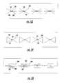
- FIG. 15is a diagrammatic plan view of a linear array of relatively ‘narrow’ printed dipole antenna elements
- FIG. 16is a diagrammatic plan view of a linear array of relatively ‘wide’ printed dipole antenna elements
- FIG. 17is a diagrammatic plan view of a linear array of printed folded dipole antenna elements
- FIG. 18is a diagrammatic plan view of a linear array of printed fan dipole antenna elements
- FIG. 19is a diagrammatic plan view of a linear array of printed bowtie dipole antenna elements
- FIG. 20is a diagrammatic plan view of a linear array of printed open sleeve dipole antenna elements
- FIGS. 1-14 of the drawingsa first non-limiting example of the application of the compact laminate antenna architecture of the invention to a four-square wideband phased array antenna array will be described.
- the inventionwill be initially described for the case of a ‘trimmed’ four-square array, shown in FIG. 1 as a linear subarray 10 of printed metalization trimmed four-square elements 11 - 1 , 11 - 2 , . . . , 11 -N.
- Each four-square element 11shown in greater detail in FIG.
- a thin, low loss dielectric support layer 15such as sheet of 28 mils thick Duroid 5870.
- the support layer 15is mounted to a first surface 16 of a relatively lightweight spacing layer 17 , such as a layer of plastic foam material (such as Rohacell 51HF foam), having a ground plane layer 18 formed on opposite surface 19 of foam spacing layer 17 .
- the thickness of lightweight foam spacing layer 17is such that, when combined with the thicknesses of the dielectric support layer 15 and those of the laminate structure, the total separation or spacing between the four-square antenna patch metalizations 11 and a ground plane metalization layer on the bottom surface of the laminate is preferably on the order of one-quarter of the wavelength of the highest frequency of operation of the array.
- each ‘trimmed’ four-square element 11 - i of the linear subarray 10 of FIG. 1is configured as four, generally square-shaped conductive (metal) components or layers 21 , 22 , 23 and 24 , that are placed closely adjacent to one another on the top surface 13 of dielectric support layer 15 in a generally square configuration, and are mutually spaced apart by narrow gaps 31 , 32 , 33 and 34 therebetween.
- the overall diagonal length D of an individual four-square element 11 - i along longitudinal dimension 12 of linear subarray 10may be on the order of one-half wavelength at the lowest frequency of operation of an antenna element.
- Each of the component-to-component gaps 31 - 34may have a width W on the order of ten mils, leaving an interior diagonal corner-to-corner spacing SD on the order of 14.14 mils, as non-limiting example.
- the input impedance of a respective trimmed four-square antenna element 11 - iis determined partially by the gap width, partially by the dimensions of its four-square components 21 - 24 , and by the height or separation of the element above the underlying ground plane 18 .
- two diametrically opposed components 21 and 23are electrically driven by means of a balanced power divider feed network to be described, at feed points 21 F and 23 F immediately their adjacent interior corners 41 and 43 .
- the physical separation or distance F between feed points 21 F and 23 Fshould be as small as possible, and is ideally equal to the diagonal gap separation between the diagonally opposed interior corners 41 and 43 of the respective driven components 21 and 23 .
- the feed points 21 F and 23 Fmay be slightly displaced from the corners of driven components 21 and 23 , so as to provide sufficient surrounding metal for the attachment of center conductors 25 of sections of the coaxial cable 26 extending through plated apertures 14 in the support layer 15 and apertures 27 in the foam spacing layer 17 , as shown diagrammatically in the side sectional view of FIG. 3 .
- the separation distance F between feed points 21 F and 23 Fmay be on the order of 86 mils.
- linear polarizationcan be produced, thereby enabling the overall array to produce a highly directive linear polarization scanning of the beam, by controlling the phase for the driven components in a conventional manner.
- the non-driven (or parasitic) and diametrically opposed ‘trimmed’ components 22 and 24 of a respective trimmed four-square trimmed antenna element 11 - iare located between the (0°/180°) driven components 21 and 23 .
- ‘trimmed’is meant that outer corner portions of the non-fed components 22 and 24 of the set of four, shown in broken lines 52 and 54 , respectively, are effectively shaped as though they have been ‘trimmed’ away.
- outer edges 62 , 64 of the two diametrically opposed, non-fed components 22 and 24are parallel to each other, and form acute angles with lines parallel to side edges of the square-shaped opposite phase-driven components 21 and 23 .
- This trimmed shapeleaves the side edges of a respective four-square element parallel to the longitudinal dimension 12 of the subarray 10 .
- a typical trim spacing or margin T between side edges 62 , 64 and parallel side edges 16 , 17 of the low loss dielectric support layer 15may be on the order of ten mils, as a non-limiting example.
- such trimmed corner-shaping of the side edges 62 and 64 of the non-driven components 22 and 24provides what is effectively a linear physical geometry of multiple trimmed four-square antenna elements 11 atop the narrow, thin dielectric support layer 15 , and thereby facilitates compactly placing multiple trimmed subarrays in a highly spatially densified side-by-side arrangement, such as that shown in FIG. 4 .
- Thisallows for placement of more trimmed-square antenna elements 11 in a direction orthogonal to a subarray array 10 than in the longitudinal dimension of a subarray, so that the frequency of operation of an overall array comprised of the trimmed four-square antenna elements of the invention can be increased relative to that of a conventional four-square architecture, thereby improving bandwidth coverage.
- a trimmed four-square arrayenjoys a frequency response that is equal to or better than a conventional non-trimmed four-square architecture.
- the compact packaging architecture of the inventiondistributes a stripline-configured power divider-feed network 70 within a laminate structure 80 , interposed between the bottom surf ace 19 of the foam support layer 17 and the ground plane layer 18 .
- the printed circuit power divider network 70is configured for the set of four, spatially successive, trimmed four-square antenna elements 11 - 1 , 11 - 2 , 11 - 3 , 11 - 4 formed atop the support layer 15 .
- power divider-feed network 70having the printed circuit configuration shown in detail in the plan view of FIG. 10, is formed on the bottom surface 81 of a first, generally stripe-shaped dielectric feed network support layer 82 .
- the dielectric support layer 82may comprise a 28 mil thick layer of Duroid 5870.
- a top surface 83 of the support layer 82has a distribution of input ports 91 , shown in FIG. 9, that are connected by conductive vias 84 through support layer 82 to various connection points of the printed circuit network 70 , as shown in the side view FIG. 6 .
- An input port 91provides an attachment location for the center conductor 25 of a section of coax cable 26 , which terminates at or abuts against the bottom surface 85 of a second generally stripe-shaped dielectric support layer 86 of the laminate structure 80 .
- Dielectric support layer 86may also comprise a 28 mil thick layer of Duroid 5870.
- a solder connection of the terminal end of the center conductor 25 of coax cable 26 to plated through hole 84may be effected by using a metallic toroid or ‘donut’ 89 .
- the bottom surface 87 of the support layer 82 and the power divider-feed network 70are laminated against top surface 88 of the second, generally stripe-shaped dielectric support layer 86 .
- a stripline ground plane metalization layer 100such as one ounce copper, is ubiquitously formed on bottom surface 85 of support layer 86 .
- the bottom surface 85 of the support layer 86contains a distribution of output ports 93 , distributed as shown in the plan view of FIG. 11 .
- the output portsare connected by way of conductive vias 94 through the support layer 85 to various connection points of the printed circuit network 70 .
- An output port 93provides an attachment location for the center conductor 95 of a section of input coax cable 96 , which terminates at or abuts against the top surface 85 of the first generally stripe-shaped dielectric support layer 82 of the laminate structure 80 .
- a solder connection of the terminal end of the center conductor 95 of coax cable 96 to plated through hole 94may be readily effected by using a metallic toroid or ‘donut’ 97 .
- the input coax cable sections 96may be ported to external drive circuitry by way of an SMA type connector, as a non-limiting example.
- the printed circuit power divider network 70is configured to include a balun 71 and an associated printed circuit branch network for the (0°/180°) feed ports of the fed components of the trimmed four-square elements of the subarray 10 .
- a first branch 72 of balun 71extends via a first printed circuit link 73 to a first pair of spaced apart, trimmed four-square subarray feed ports 21 F- 1 , 23 F- 2 for the first driven components 21 of respective first and second trimmed four-square antenna elements 11 - 1 , 11 - 2 atop support layer 15 .
- a second printed circuit link 74extends from the balun 71 to a second pair of spaced apart feed ports for 21 F- 3 , 21 F- 4 of driven components 21 of respective third and fourth second trimmed four-square elements 11 - 3 , 11 - 4 .
- a third printed circuit link 76extends from a second branch 75 of balun 71 to a third pair of spaced apart, the trimmed component feed ports 23 F- 1 , 23 F- 2 for the driven components 23 of the first and second trimmed four-square elements 11 - 1 , 11 - 2 .
- a fourth printed circuit link 77extends from the balun to a fourth pair of spaced apart feed ports 23 F- 3 , 23 F- 4 for the driven components 23 of the third and fourth trimmed four-square elements 11 - 3 , 11 - 4 .
- FIGS. 12 and 13depict, in solid lines, respective E- and H-plane co-polarized antenna patterns of a trimmed four-square element in accordance with the invention. Shown in broken lines are associated E- and H- plane patterns approximated using a Cos q ( ⁇ ) pattern (for 0° less than or equal to ⁇ , and ⁇ less than or equal to 90°. The value for q is equal to the ratio: log(F( ⁇ ))/log(cos ⁇ ), where ⁇ is taken at ⁇ 10 dB points. The cos q ( ⁇ ) assumes no backplane radiation. In the co-polarized E-plane radiation pattern of FIG.
- FIG. 14which is a plot of impedance vs frequency of a trimmed four-square antenna element, shows that its impedance characteristics are equal to or better than those of a conventional non-trimmed four-square element.
- FIG. 15shows a linear array of relatively ‘narrow’ printed dipole antenna elements 150 , whose feed ports 151 , 152 are spatially positioned in effectively the same geometry as the feed ports 23 of the trimmed four-square arrangement of FIGS. 1-14, and may be readily mated with the underlying feed network laminate structure of the trimmed four-square embodiment.
- FIG. 16shows a linear array of relatively ‘wide’ printed dipole antenna elements 160 having similarly spatially located feed ports 161 , 162 .
- FIG. 17shows a linear array of printed folded dipole antenna elements 170 having adjacent pairs of feed ports 171 , 172
- FIG. 18shows a linear array of printed fan dipole antenna elements 180 with pairs of feed ports 181 , 182 .
- FIG. 19shows a linear array of printed bowtie dipole antenna elements 190 having closely spaced feed ports 191 , 192
- FIG. 20shows a linear array of printed open sleeve dipole antenna elements 200 with adjacent feed ports 201 , 202 .
Landscapes
- Variable-Direction Aerials And Aerial Arrays (AREA)
Abstract
Description
Claims (9)
Priority Applications (1)
| Application Number | Priority Date | Filing Date | Title |
|---|---|---|---|
| US09/477,853US6300906B1 (en) | 2000-01-05 | 2000-01-05 | Wideband phased array antenna employing increased packaging density laminate structure containing feed network, balun and power divider circuitry |
Applications Claiming Priority (1)
| Application Number | Priority Date | Filing Date | Title |
|---|---|---|---|
| US09/477,853US6300906B1 (en) | 2000-01-05 | 2000-01-05 | Wideband phased array antenna employing increased packaging density laminate structure containing feed network, balun and power divider circuitry |
Publications (1)
| Publication Number | Publication Date |
|---|---|
| US6300906B1true US6300906B1 (en) | 2001-10-09 |
Family
ID=23897610
Family Applications (1)
| Application Number | Title | Priority Date | Filing Date |
|---|---|---|---|
| US09/477,853Expired - LifetimeUS6300906B1 (en) | 2000-01-05 | 2000-01-05 | Wideband phased array antenna employing increased packaging density laminate structure containing feed network, balun and power divider circuitry |
Country Status (1)
| Country | Link |
|---|---|
| US (1) | US6300906B1 (en) |
Cited By (172)
| Publication number | Priority date | Publication date | Assignee | Title |
|---|---|---|---|---|
| WO2002001668A3 (en)* | 2000-06-28 | 2002-06-27 | Penn State Res Found | Miniaturized conformal wideband fractal antennas on high dielectric substrates and chiral layers |
| US20030036674A1 (en)* | 2001-07-26 | 2003-02-20 | Bouton Chad Edward | Electromagnetic sensors for biological tissue applications and methods for their use |
| WO2003050917A1 (en)* | 2001-12-07 | 2003-06-19 | Skycross, Inc. | Multiple antenna diversity for wireless lan applications |
| US20040080465A1 (en)* | 2002-08-22 | 2004-04-29 | Hendler Jason M. | Apparatus and method for forming a monolithic surface-mountable antenna |
| US20040090389A1 (en)* | 2002-08-19 | 2004-05-13 | Young-Min Jo | Compact, low profile, circular polarization cubic antenna |
| US20040125020A1 (en)* | 2002-06-04 | 2004-07-01 | Hendler Jason M. | Wideband printed monopole antenna |
| US20050007286A1 (en)* | 2003-07-11 | 2005-01-13 | Trott Keith D. | Wideband phased array radiator |
| US6885343B2 (en) | 2002-09-26 | 2005-04-26 | Andrew Corporation | Stripline parallel-series-fed proximity-coupled cavity backed patch antenna array |
| FR2865072A1 (en)* | 2003-11-17 | 2005-07-15 | Bosch Gmbh Robert | LAYER CONSTRUCTED SYMMETRIC ANTENNA DEVICE |
| US20060038732A1 (en)* | 2003-07-11 | 2006-02-23 | Deluca Mark R | Broadband dual polarized slotline feed circuit |
| US20070075903A1 (en)* | 2005-10-03 | 2007-04-05 | Denso Corporation | Antenna, radio device, method of designing antenna, and nethod of measuring operating frequency of antenna |
| US20070123770A1 (en)* | 2003-10-24 | 2007-05-31 | Medrad Inc. | System for detecting fluid changes and sensoring devices therefor |
| US20070188398A1 (en)* | 2006-02-13 | 2007-08-16 | Itt Manufacturing Enterprises, Inc. | High power, polarization-diverse cloverleaf phased array |
| US20080252544A1 (en)* | 2007-04-12 | 2008-10-16 | Irion James M | Low Profile Antenna |
| US20090009391A1 (en)* | 2005-06-09 | 2009-01-08 | Macdonald Dettwiler And Associates Ltd. | Lightweight Space-Fed Active Phased Array Antenna System |
| US20090073075A1 (en)* | 2007-09-18 | 2009-03-19 | Irion Ii James M | Dual Polarized Low Profile Antenna |
| US20100007561A1 (en)* | 2008-05-23 | 2010-01-14 | Steven Bucca | Broadband patch antenna and antenna system |
| WO2010112857A1 (en)* | 2009-03-31 | 2010-10-07 | The University Of Manchester | Wide band array antenna |
| US20110148725A1 (en)* | 2009-12-22 | 2011-06-23 | Raytheon Company | Methods and apparatus for coincident phase center broadband radiator |
| US8059033B2 (en)* | 2008-01-15 | 2011-11-15 | Nokia Siemens Networks Gmbh & Co. Kg | Patch antenna |
| US20120032869A1 (en)* | 2010-08-09 | 2012-02-09 | Hawkins Terrance J | Frequency scalable low profile broadband quad-fed patch element and array |
| US8169371B1 (en)* | 2009-08-14 | 2012-05-01 | The United States of America, as represented by the Administrator of the National Aeronautics and Space Administrator | Metal patch antenna |
| US8195118B2 (en) | 2008-07-15 | 2012-06-05 | Linear Signal, Inc. | Apparatus, system, and method for integrated phase shifting and amplitude control of phased array signals |
| US20120293381A1 (en)* | 2011-05-17 | 2012-11-22 | Apostolos John T | Wide band embedded armor antenna |
| US20120293380A1 (en)* | 2011-05-17 | 2012-11-22 | Apostolos John T | Wide band embedded armor antenna |
| CN103066382A (en)* | 2012-12-18 | 2013-04-24 | 张家港保税区国信通信有限公司 | Low-profile ultra-wideband dual-band dual-polarization antenna for mobile communications |
| US8872719B2 (en) | 2009-11-09 | 2014-10-28 | Linear Signal, Inc. | Apparatus, system, and method for integrated modular phased array tile configuration |
| US20150116169A1 (en)* | 2013-10-31 | 2015-04-30 | Sony Corporation | MM Wave Antenna Array Integrated with Cellular Antenna |
| US9289550B1 (en) | 2001-02-06 | 2016-03-22 | Bayer Healthcare Llc | Apparatus and method for detecting fluid extravasation |
| US9667317B2 (en) | 2015-06-15 | 2017-05-30 | At&T Intellectual Property I, L.P. | Method and apparatus for providing security using network traffic adjustments |
| US9674711B2 (en) | 2013-11-06 | 2017-06-06 | At&T Intellectual Property I, L.P. | Surface-wave communications and methods thereof |
| US9685992B2 (en) | 2014-10-03 | 2017-06-20 | At&T Intellectual Property I, L.P. | Circuit panel network and methods thereof |
| US9705561B2 (en) | 2015-04-24 | 2017-07-11 | At&T Intellectual Property I, L.P. | Directional coupling device and methods for use therewith |
| US9705610B2 (en) | 2014-10-21 | 2017-07-11 | At&T Intellectual Property I, L.P. | Transmission device with impairment compensation and methods for use therewith |
| US9722318B2 (en) | 2015-07-14 | 2017-08-01 | At&T Intellectual Property I, L.P. | Method and apparatus for coupling an antenna to a device |
| US9729197B2 (en) | 2015-10-01 | 2017-08-08 | At&T Intellectual Property I, L.P. | Method and apparatus for communicating network management traffic over a network |
| US9735833B2 (en) | 2015-07-31 | 2017-08-15 | At&T Intellectual Property I, L.P. | Method and apparatus for communications management in a neighborhood network |
| US9742521B2 (en) | 2014-11-20 | 2017-08-22 | At&T Intellectual Property I, L.P. | Transmission device with mode division multiplexing and methods for use therewith |
| US9742462B2 (en) | 2014-12-04 | 2017-08-22 | At&T Intellectual Property I, L.P. | Transmission medium and communication interfaces and methods for use therewith |
| US9748626B2 (en) | 2015-05-14 | 2017-08-29 | At&T Intellectual Property I, L.P. | Plurality of cables having different cross-sectional shapes which are bundled together to form a transmission medium |
| US9749013B2 (en) | 2015-03-17 | 2017-08-29 | At&T Intellectual Property I, L.P. | Method and apparatus for reducing attenuation of electromagnetic waves guided by a transmission medium |
| US9749053B2 (en) | 2015-07-23 | 2017-08-29 | At&T Intellectual Property I, L.P. | Node device, repeater and methods for use therewith |
| US9768833B2 (en) | 2014-09-15 | 2017-09-19 | At&T Intellectual Property I, L.P. | Method and apparatus for sensing a condition in a transmission medium of electromagnetic waves |
| US9769128B2 (en) | 2015-09-28 | 2017-09-19 | At&T Intellectual Property I, L.P. | Method and apparatus for encryption of communications over a network |
| US9769020B2 (en) | 2014-10-21 | 2017-09-19 | At&T Intellectual Property I, L.P. | Method and apparatus for responding to events affecting communications in a communication network |
| US9780834B2 (en) | 2014-10-21 | 2017-10-03 | At&T Intellectual Property I, L.P. | Method and apparatus for transmitting electromagnetic waves |
| US9787412B2 (en) | 2015-06-25 | 2017-10-10 | At&T Intellectual Property I, L.P. | Methods and apparatus for inducing a fundamental wave mode on a transmission medium |
| US9793955B2 (en) | 2015-04-24 | 2017-10-17 | At&T Intellectual Property I, Lp | Passive electrical coupling device and methods for use therewith |
| US9793954B2 (en) | 2015-04-28 | 2017-10-17 | At&T Intellectual Property I, L.P. | Magnetic coupling device and methods for use therewith |
| US9793951B2 (en) | 2015-07-15 | 2017-10-17 | At&T Intellectual Property I, L.P. | Method and apparatus for launching a wave mode that mitigates interference |
| US9800327B2 (en) | 2014-11-20 | 2017-10-24 | At&T Intellectual Property I, L.P. | Apparatus for controlling operations of a communication device and methods thereof |
| US20170310016A1 (en)* | 2014-10-21 | 2017-10-26 | Nec Corporation | Planar antenna |
| US9820146B2 (en) | 2015-06-12 | 2017-11-14 | At&T Intellectual Property I, L.P. | Method and apparatus for authentication and identity management of communicating devices |
| US9838078B2 (en) | 2015-07-31 | 2017-12-05 | At&T Intellectual Property I, L.P. | Method and apparatus for exchanging communication signals |
| US9838896B1 (en) | 2016-12-09 | 2017-12-05 | At&T Intellectual Property I, L.P. | Method and apparatus for assessing network coverage |
| US9847850B2 (en) | 2014-10-14 | 2017-12-19 | At&T Intellectual Property I, L.P. | Method and apparatus for adjusting a mode of communication in a communication network |
| US9847566B2 (en) | 2015-07-14 | 2017-12-19 | At&T Intellectual Property I, L.P. | Method and apparatus for adjusting a field of a signal to mitigate interference |
| US9853342B2 (en) | 2015-07-14 | 2017-12-26 | At&T Intellectual Property I, L.P. | Dielectric transmission medium connector and methods for use therewith |
| US9860075B1 (en) | 2016-08-26 | 2018-01-02 | At&T Intellectual Property I, L.P. | Method and communication node for broadband distribution |
| US9865911B2 (en) | 2015-06-25 | 2018-01-09 | At&T Intellectual Property I, L.P. | Waveguide system for slot radiating first electromagnetic waves that are combined into a non-fundamental wave mode second electromagnetic wave on a transmission medium |
| US9866309B2 (en) | 2015-06-03 | 2018-01-09 | At&T Intellectual Property I, Lp | Host node device and methods for use therewith |
| US9866276B2 (en) | 2014-10-10 | 2018-01-09 | At&T Intellectual Property I, L.P. | Method and apparatus for arranging communication sessions in a communication system |
| US9871558B2 (en) | 2014-10-21 | 2018-01-16 | At&T Intellectual Property I, L.P. | Guided-wave transmission device and methods for use therewith |
| US9871282B2 (en) | 2015-05-14 | 2018-01-16 | At&T Intellectual Property I, L.P. | At least one transmission medium having a dielectric surface that is covered at least in part by a second dielectric |
| US9871283B2 (en) | 2015-07-23 | 2018-01-16 | At&T Intellectual Property I, Lp | Transmission medium having a dielectric core comprised of plural members connected by a ball and socket configuration |
| US9876264B2 (en) | 2015-10-02 | 2018-01-23 | At&T Intellectual Property I, Lp | Communication system, guided wave switch and methods for use therewith |
| US9876605B1 (en) | 2016-10-21 | 2018-01-23 | At&T Intellectual Property I, L.P. | Launcher and coupling system to support desired guided wave mode |
| US9876570B2 (en) | 2015-02-20 | 2018-01-23 | At&T Intellectual Property I, Lp | Guided-wave transmission device with non-fundamental mode propagation and methods for use therewith |
| US9882257B2 (en) | 2015-07-14 | 2018-01-30 | At&T Intellectual Property I, L.P. | Method and apparatus for launching a wave mode that mitigates interference |
| US9887447B2 (en) | 2015-05-14 | 2018-02-06 | At&T Intellectual Property I, L.P. | Transmission medium having multiple cores and methods for use therewith |
| US9893795B1 (en) | 2016-12-07 | 2018-02-13 | At&T Intellectual Property I, Lp | Method and repeater for broadband distribution |
| US9906269B2 (en) | 2014-09-17 | 2018-02-27 | At&T Intellectual Property I, L.P. | Monitoring and mitigating conditions in a communication network |
| US9904535B2 (en) | 2015-09-14 | 2018-02-27 | At&T Intellectual Property I, L.P. | Method and apparatus for distributing software |
| US9912381B2 (en) | 2015-06-03 | 2018-03-06 | At&T Intellectual Property I, Lp | Network termination and methods for use therewith |
| US9912027B2 (en) | 2015-07-23 | 2018-03-06 | At&T Intellectual Property I, L.P. | Method and apparatus for exchanging communication signals |
| US9911020B1 (en) | 2016-12-08 | 2018-03-06 | At&T Intellectual Property I, L.P. | Method and apparatus for tracking via a radio frequency identification device |
| US9912033B2 (en) | 2014-10-21 | 2018-03-06 | At&T Intellectual Property I, Lp | Guided wave coupler, coupling module and methods for use therewith |
| US9913139B2 (en) | 2015-06-09 | 2018-03-06 | At&T Intellectual Property I, L.P. | Signal fingerprinting for authentication of communicating devices |
| US9917341B2 (en) | 2015-05-27 | 2018-03-13 | At&T Intellectual Property I, L.P. | Apparatus and method for launching electromagnetic waves and for modifying radial dimensions of the propagating electromagnetic waves |
| US9929755B2 (en) | 2015-07-14 | 2018-03-27 | At&T Intellectual Property I, L.P. | Method and apparatus for coupling an antenna to a device |
| US9927517B1 (en) | 2016-12-06 | 2018-03-27 | At&T Intellectual Property I, L.P. | Apparatus and methods for sensing rainfall |
| US9948333B2 (en) | 2015-07-23 | 2018-04-17 | At&T Intellectual Property I, L.P. | Method and apparatus for wireless communications to mitigate interference |
| US9954286B2 (en) | 2014-10-21 | 2018-04-24 | At&T Intellectual Property I, L.P. | Guided-wave transmission device with non-fundamental mode propagation and methods for use therewith |
| US9954287B2 (en) | 2014-11-20 | 2018-04-24 | At&T Intellectual Property I, L.P. | Apparatus for converting wireless signals and electromagnetic waves and methods thereof |
| US9967173B2 (en) | 2015-07-31 | 2018-05-08 | At&T Intellectual Property I, L.P. | Method and apparatus for authentication and identity management of communicating devices |
| US9973940B1 (en) | 2017-02-27 | 2018-05-15 | At&T Intellectual Property I, L.P. | Apparatus and methods for dynamic impedance matching of a guided wave launcher |
| US9973416B2 (en) | 2014-10-02 | 2018-05-15 | At&T Intellectual Property I, L.P. | Method and apparatus that provides fault tolerance in a communication network |
| US9991580B2 (en) | 2016-10-21 | 2018-06-05 | At&T Intellectual Property I, L.P. | Launcher and coupling system for guided wave mode cancellation |
| US9991605B2 (en) | 2015-06-16 | 2018-06-05 | The Mitre Corporation | Frequency-scaled ultra-wide spectrum element |
| US9997819B2 (en) | 2015-06-09 | 2018-06-12 | At&T Intellectual Property I, L.P. | Transmission medium and method for facilitating propagation of electromagnetic waves via a core |
| US9999038B2 (en) | 2013-05-31 | 2018-06-12 | At&T Intellectual Property I, L.P. | Remote distributed antenna system |
| US9998870B1 (en) | 2016-12-08 | 2018-06-12 | At&T Intellectual Property I, L.P. | Method and apparatus for proximity sensing |
| US10009067B2 (en) | 2014-12-04 | 2018-06-26 | At&T Intellectual Property I, L.P. | Method and apparatus for configuring a communication interface |
| US10020844B2 (en) | 2016-12-06 | 2018-07-10 | T&T Intellectual Property I, L.P. | Method and apparatus for broadcast communication via guided waves |
| US10027397B2 (en) | 2016-12-07 | 2018-07-17 | At&T Intellectual Property I, L.P. | Distributed antenna system and methods for use therewith |
| US10044409B2 (en) | 2015-07-14 | 2018-08-07 | At&T Intellectual Property I, L.P. | Transmission medium and methods for use therewith |
| US10051630B2 (en) | 2013-05-31 | 2018-08-14 | At&T Intellectual Property I, L.P. | Remote distributed antenna system |
| US10056699B2 (en) | 2015-06-16 | 2018-08-21 | The Mitre Cooperation | Substrate-loaded frequency-scaled ultra-wide spectrum element |
| US10069185B2 (en) | 2015-06-25 | 2018-09-04 | At&T Intellectual Property I, L.P. | Methods and apparatus for inducing a non-fundamental wave mode on a transmission medium |
| US10069535B2 (en) | 2016-12-08 | 2018-09-04 | At&T Intellectual Property I, L.P. | Apparatus and methods for launching electromagnetic waves having a certain electric field structure |
| US10090594B2 (en) | 2016-11-23 | 2018-10-02 | At&T Intellectual Property I, L.P. | Antenna system having structural configurations for assembly |
| US10090606B2 (en) | 2015-07-15 | 2018-10-02 | At&T Intellectual Property I, L.P. | Antenna system with dielectric array and methods for use therewith |
| US10103422B2 (en) | 2016-12-08 | 2018-10-16 | At&T Intellectual Property I, L.P. | Method and apparatus for mounting network devices |
| US10135145B2 (en) | 2016-12-06 | 2018-11-20 | At&T Intellectual Property I, L.P. | Apparatus and methods for generating an electromagnetic wave along a transmission medium |
| US10135147B2 (en) | 2016-10-18 | 2018-11-20 | At&T Intellectual Property I, L.P. | Apparatus and methods for launching guided waves via an antenna |
| US10135146B2 (en) | 2016-10-18 | 2018-11-20 | At&T Intellectual Property I, L.P. | Apparatus and methods for launching guided waves via circuits |
| US10139820B2 (en) | 2016-12-07 | 2018-11-27 | At&T Intellectual Property I, L.P. | Method and apparatus for deploying equipment of a communication system |
| US10148016B2 (en) | 2015-07-14 | 2018-12-04 | At&T Intellectual Property I, L.P. | Apparatus and methods for communicating utilizing an antenna array |
| US10158180B1 (en)* | 2015-08-05 | 2018-12-18 | Northrop Grumman Systems Corporation | Ultrawideband nested bowtie array |
| US10168695B2 (en) | 2016-12-07 | 2019-01-01 | At&T Intellectual Property I, L.P. | Method and apparatus for controlling an unmanned aircraft |
| US10178445B2 (en) | 2016-11-23 | 2019-01-08 | At&T Intellectual Property I, L.P. | Methods, devices, and systems for load balancing between a plurality of waveguides |
| US10205655B2 (en) | 2015-07-14 | 2019-02-12 | At&T Intellectual Property I, L.P. | Apparatus and methods for communicating utilizing an antenna array and multiple communication paths |
| US10225025B2 (en) | 2016-11-03 | 2019-03-05 | At&T Intellectual Property I, L.P. | Method and apparatus for detecting a fault in a communication system |
| US10224634B2 (en) | 2016-11-03 | 2019-03-05 | At&T Intellectual Property I, L.P. | Methods and apparatus for adjusting an operational characteristic of an antenna |
| US10243784B2 (en) | 2014-11-20 | 2019-03-26 | At&T Intellectual Property I, L.P. | System for generating topology information and methods thereof |
| US10243270B2 (en) | 2016-12-07 | 2019-03-26 | At&T Intellectual Property I, L.P. | Beam adaptive multi-feed dielectric antenna system and methods for use therewith |
| US10243265B2 (en) | 2013-08-08 | 2019-03-26 | The University Of Manchester | Wide band array antenna |
| US10264586B2 (en) | 2016-12-09 | 2019-04-16 | At&T Mobility Ii Llc | Cloud-based packet controller and methods for use therewith |
| US10291334B2 (en) | 2016-11-03 | 2019-05-14 | At&T Intellectual Property I, L.P. | System for detecting a fault in a communication system |
| US10298293B2 (en) | 2017-03-13 | 2019-05-21 | At&T Intellectual Property I, L.P. | Apparatus of communication utilizing wireless network devices |
| US10305190B2 (en) | 2016-12-01 | 2019-05-28 | At&T Intellectual Property I, L.P. | Reflecting dielectric antenna system and methods for use therewith |
| US10312567B2 (en) | 2016-10-26 | 2019-06-04 | At&T Intellectual Property I, L.P. | Launcher with planar strip antenna and methods for use therewith |
| US10320586B2 (en) | 2015-07-14 | 2019-06-11 | At&T Intellectual Property I, L.P. | Apparatus and methods for generating non-interfering electromagnetic waves on an insulated transmission medium |
| US10326494B2 (en) | 2016-12-06 | 2019-06-18 | At&T Intellectual Property I, L.P. | Apparatus for measurement de-embedding and methods for use therewith |
| US10326689B2 (en) | 2016-12-08 | 2019-06-18 | At&T Intellectual Property I, L.P. | Method and system for providing alternative communication paths |
| US10340983B2 (en) | 2016-12-09 | 2019-07-02 | At&T Intellectual Property I, L.P. | Method and apparatus for surveying remote sites via guided wave communications |
| US10340601B2 (en) | 2016-11-23 | 2019-07-02 | At&T Intellectual Property I, L.P. | Multi-antenna system and methods for use therewith |
| US10340600B2 (en) | 2016-10-18 | 2019-07-02 | At&T Intellectual Property I, L.P. | Apparatus and methods for launching guided waves via plural waveguide systems |
| US10340603B2 (en) | 2016-11-23 | 2019-07-02 | At&T Intellectual Property I, L.P. | Antenna system having shielded structural configurations for assembly |
| US10340573B2 (en) | 2016-10-26 | 2019-07-02 | At&T Intellectual Property I, L.P. | Launcher with cylindrical coupling device and methods for use therewith |
| US10355367B2 (en) | 2015-10-16 | 2019-07-16 | At&T Intellectual Property I, L.P. | Antenna structure for exchanging wireless signals |
| US10361489B2 (en) | 2016-12-01 | 2019-07-23 | At&T Intellectual Property I, L.P. | Dielectric dish antenna system and methods for use therewith |
| US10359749B2 (en) | 2016-12-07 | 2019-07-23 | At&T Intellectual Property I, L.P. | Method and apparatus for utilities management via guided wave communication |
| US10374316B2 (en) | 2016-10-21 | 2019-08-06 | At&T Intellectual Property I, L.P. | System and dielectric antenna with non-uniform dielectric |
| US10382976B2 (en) | 2016-12-06 | 2019-08-13 | At&T Intellectual Property I, L.P. | Method and apparatus for managing wireless communications based on communication paths and network device positions |
| US10389037B2 (en) | 2016-12-08 | 2019-08-20 | At&T Intellectual Property I, L.P. | Apparatus and methods for selecting sections of an antenna array and use therewith |
| US10389029B2 (en) | 2016-12-07 | 2019-08-20 | At&T Intellectual Property I, L.P. | Multi-feed dielectric antenna system with core selection and methods for use therewith |
| US10411356B2 (en) | 2016-12-08 | 2019-09-10 | At&T Intellectual Property I, L.P. | Apparatus and methods for selectively targeting communication devices with an antenna array |
| US10439675B2 (en) | 2016-12-06 | 2019-10-08 | At&T Intellectual Property I, L.P. | Method and apparatus for repeating guided wave communication signals |
| US10446936B2 (en) | 2016-12-07 | 2019-10-15 | At&T Intellectual Property I, L.P. | Multi-feed dielectric antenna system and methods for use therewith |
| US20190334255A1 (en)* | 2018-04-25 | 2019-10-31 | Bae Systems Information And Electronic Systems Integration Inc. | Modular/scalable antenna array design |
| US10498044B2 (en) | 2016-11-03 | 2019-12-03 | At&T Intellectual Property I, L.P. | Apparatus for configuring a surface of an antenna |
| US10530505B2 (en) | 2016-12-08 | 2020-01-07 | At&T Intellectual Property I, L.P. | Apparatus and methods for launching electromagnetic waves along a transmission medium |
| US10535928B2 (en) | 2016-11-23 | 2020-01-14 | At&T Intellectual Property I, L.P. | Antenna system and methods for use therewith |
| US10547348B2 (en) | 2016-12-07 | 2020-01-28 | At&T Intellectual Property I, L.P. | Method and apparatus for switching transmission mediums in a communication system |
| US10601494B2 (en) | 2016-12-08 | 2020-03-24 | At&T Intellectual Property I, L.P. | Dual-band communication device and method for use therewith |
| US10637149B2 (en) | 2016-12-06 | 2020-04-28 | At&T Intellectual Property I, L.P. | Injection molded dielectric antenna and methods for use therewith |
| US10650940B2 (en) | 2015-05-15 | 2020-05-12 | At&T Intellectual Property I, L.P. | Transmission medium having a conductive material and methods for use therewith |
| US10666302B2 (en)* | 2016-06-21 | 2020-05-26 | Telefonaktiebolaget Lm Ericsson (Publ) | Antenna feed in a wireless communication network node |
| US10694379B2 (en) | 2016-12-06 | 2020-06-23 | At&T Intellectual Property I, L.P. | Waveguide system with device-based authentication and methods for use therewith |
| US10727599B2 (en) | 2016-12-06 | 2020-07-28 | At&T Intellectual Property I, L.P. | Launcher with slot antenna and methods for use therewith |
| US10722136B2 (en) | 2011-09-02 | 2020-07-28 | Battelle Memorial Institute | Wireless and power-source-free extravasation and infiltration detection sensor |
| US10755542B2 (en) | 2016-12-06 | 2020-08-25 | At&T Intellectual Property I, L.P. | Method and apparatus for surveillance via guided wave communication |
| US10777873B2 (en) | 2016-12-08 | 2020-09-15 | At&T Intellectual Property I, L.P. | Method and apparatus for mounting network devices |
| US10797781B2 (en) | 2015-06-03 | 2020-10-06 | At&T Intellectual Property I, L.P. | Client node device and methods for use therewith |
| US10811767B2 (en) | 2016-10-21 | 2020-10-20 | At&T Intellectual Property I, L.P. | System and dielectric antenna with convex dielectric radome |
| US10819035B2 (en) | 2016-12-06 | 2020-10-27 | At&T Intellectual Property I, L.P. | Launcher with helical antenna and methods for use therewith |
| US10854993B2 (en) | 2017-09-18 | 2020-12-01 | The Mitre Corporation | Low-profile, wideband electronically scanned array for geo-location, communications, and radar |
| US10886625B2 (en) | 2018-08-28 | 2021-01-05 | The Mitre Corporation | Low-profile wideband antenna array configured to utilize efficient manufacturing processes |
| CN112262500A (en)* | 2018-04-11 | 2021-01-22 | 高通股份有限公司 | Patch antenna array |
| US10910730B2 (en) | 2018-06-07 | 2021-02-02 | Helmuth G. Bachmann | Attachable antenna field director for omnidirectional drone antennas |
| US10916969B2 (en) | 2016-12-08 | 2021-02-09 | At&T Intellectual Property I, L.P. | Method and apparatus for providing power using an inductive coupling |
| US10938108B2 (en) | 2016-12-08 | 2021-03-02 | At&T Intellectual Property I, L.P. | Frequency selective multi-feed dielectric antenna system and methods for use therewith |
| US11004801B2 (en) | 2019-08-28 | 2021-05-11 | Amkor Technology Singapore Holding Pte. Ltd. | Semiconductor devices and methods of manufacturing semiconductor devices |
| CN112909491A (en)* | 2021-01-21 | 2021-06-04 | 福耀玻璃工业集团股份有限公司 | Be applied to on-vehicle glass antenna |
| US20220131270A1 (en)* | 2020-10-26 | 2022-04-28 | Avx Antenna, Inc. D/B/A Ethertronics, Inc. | Wideband Phased Array Antenna For Millimeter Wave Communications |
| US11355451B2 (en) | 2019-08-28 | 2022-06-07 | Amkor Technology Singapore Holding Pte. Ltd. | Semiconductor devices and methods of manufacturing semiconductor devices |
| CN114665280A (en)* | 2022-03-28 | 2022-06-24 | 中国电子科技集团公司第十研究所 | Three-dimensional transmitting-receiving feed network applied to flat-panel packaged array antenna |
| US20230163470A1 (en)* | 2021-11-19 | 2023-05-25 | Wistron Neweb Corp. | Communication device |
| US12095497B2 (en) | 2021-05-26 | 2024-09-17 | Skyworks Solutions, Inc. | Signal conditioning circuits for coupling to antenna |
| US12249766B2 (en)* | 2021-11-30 | 2025-03-11 | Viettel Group | Wide bandwidth dual polarized array antenna using orthogonal feeding technique |
| US12272887B2 (en)* | 2022-02-18 | 2025-04-08 | Mediatek Inc. | Antenna |
Citations (7)
| Publication number | Priority date | Publication date | Assignee | Title |
|---|---|---|---|---|
| US3681769A (en) | 1970-07-30 | 1972-08-01 | Itt | Dual polarized printed circuit dipole antenna array |
| US4825220A (en) | 1986-11-26 | 1989-04-25 | General Electric Company | Microstrip fed printed dipole with an integral balun |
| US4973972A (en) | 1989-09-07 | 1990-11-27 | The United States Of America As Represented By The Administrator Of The National Aeronautics And Space Adminstration | Stripline feed for a microstrip array of patch elements with teardrop shaped probes |
| US5036335A (en) | 1989-06-09 | 1991-07-30 | The Marconi Company Limited | Tapered slot antenna with balun slot line and stripline feed |
| US5572172A (en) | 1995-08-09 | 1996-11-05 | Qualcomm Incorporated | 180° power divider for a helix antenna |
| US5896107A (en)* | 1997-05-27 | 1999-04-20 | Allen Telecom Inc. | Dual polarized aperture coupled microstrip patch antenna system |
| US5926137A (en) | 1997-06-30 | 1999-07-20 | Virginia Tech Intellectual Properties | Foursquare antenna radiating element |
- 2000
- 2000-01-05USUS09/477,853patent/US6300906B1/ennot_activeExpired - Lifetime
Patent Citations (7)
| Publication number | Priority date | Publication date | Assignee | Title |
|---|---|---|---|---|
| US3681769A (en) | 1970-07-30 | 1972-08-01 | Itt | Dual polarized printed circuit dipole antenna array |
| US4825220A (en) | 1986-11-26 | 1989-04-25 | General Electric Company | Microstrip fed printed dipole with an integral balun |
| US5036335A (en) | 1989-06-09 | 1991-07-30 | The Marconi Company Limited | Tapered slot antenna with balun slot line and stripline feed |
| US4973972A (en) | 1989-09-07 | 1990-11-27 | The United States Of America As Represented By The Administrator Of The National Aeronautics And Space Adminstration | Stripline feed for a microstrip array of patch elements with teardrop shaped probes |
| US5572172A (en) | 1995-08-09 | 1996-11-05 | Qualcomm Incorporated | 180° power divider for a helix antenna |
| US5896107A (en)* | 1997-05-27 | 1999-04-20 | Allen Telecom Inc. | Dual polarized aperture coupled microstrip patch antenna system |
| US5926137A (en) | 1997-06-30 | 1999-07-20 | Virginia Tech Intellectual Properties | Foursquare antenna radiating element |
Non-Patent Citations (1)
| Title |
|---|
| Article From Ph.D. Thesis Entitled: Analysis Of Infinite Arrays Of Arbitrarily Shaped Planar Radiating Elements Usining A Floquet Mode Based Method Of Moments Approach, by James William LaPean, Jr. et al, Virginia Polytechnic Institute and State University, 1996, pp. 114-116. |
Cited By (229)
| Publication number | Priority date | Publication date | Assignee | Title |
|---|---|---|---|---|
| US6525691B2 (en) | 2000-06-28 | 2003-02-25 | The Penn State Research Foundation | Miniaturized conformal wideband fractal antennas on high dielectric substrates and chiral layers |
| WO2002001668A3 (en)* | 2000-06-28 | 2002-06-27 | Penn State Res Found | Miniaturized conformal wideband fractal antennas on high dielectric substrates and chiral layers |
| US9289550B1 (en) | 2001-02-06 | 2016-03-22 | Bayer Healthcare Llc | Apparatus and method for detecting fluid extravasation |
| US7591792B2 (en)* | 2001-07-26 | 2009-09-22 | Medrad, Inc. | Electromagnetic sensors for biological tissue applications and methods for their use |
| US20030036674A1 (en)* | 2001-07-26 | 2003-02-20 | Bouton Chad Edward | Electromagnetic sensors for biological tissue applications and methods for their use |
| WO2003050917A1 (en)* | 2001-12-07 | 2003-06-19 | Skycross, Inc. | Multiple antenna diversity for wireless lan applications |
| US20030146876A1 (en)* | 2001-12-07 | 2003-08-07 | Greer Kerry L. | Multiple antenna diversity for wireless LAN applications |
| US7253779B2 (en) | 2001-12-07 | 2007-08-07 | Skycross, Inc. | Multiple antenna diversity for wireless LAN applications |
| US6937193B2 (en) | 2002-06-04 | 2005-08-30 | Skycross, Inc. | Wideband printed monopole antenna |
| US20040125020A1 (en)* | 2002-06-04 | 2004-07-01 | Hendler Jason M. | Wideband printed monopole antenna |
| US6888510B2 (en) | 2002-08-19 | 2005-05-03 | Skycross, Inc. | Compact, low profile, circular polarization cubic antenna |
| US20040090389A1 (en)* | 2002-08-19 | 2004-05-13 | Young-Min Jo | Compact, low profile, circular polarization cubic antenna |
| US20040080465A1 (en)* | 2002-08-22 | 2004-04-29 | Hendler Jason M. | Apparatus and method for forming a monolithic surface-mountable antenna |
| US6950066B2 (en) | 2002-08-22 | 2005-09-27 | Skycross, Inc. | Apparatus and method for forming a monolithic surface-mountable antenna |
| US6885343B2 (en) | 2002-09-26 | 2005-04-26 | Andrew Corporation | Stripline parallel-series-fed proximity-coupled cavity backed patch antenna array |
| US20050007286A1 (en)* | 2003-07-11 | 2005-01-13 | Trott Keith D. | Wideband phased array radiator |
| US7180457B2 (en) | 2003-07-11 | 2007-02-20 | Raytheon Company | Wideband phased array radiator |
| US20060038732A1 (en)* | 2003-07-11 | 2006-02-23 | Deluca Mark R | Broadband dual polarized slotline feed circuit |
| US8295920B2 (en) | 2003-10-24 | 2012-10-23 | Medrad, Inc. | System for detecting fluid changes and sensoring devices therefor |
| US20070123770A1 (en)* | 2003-10-24 | 2007-05-31 | Medrad Inc. | System for detecting fluid changes and sensoring devices therefor |
| EP1675506A4 (en)* | 2003-10-24 | 2010-06-23 | Medrad Inc | SYSTEMS FOR DETECTING FLUID VARIATIONS AND CORRESPONDING DETECTION DEVICES |
| FR2865072A1 (en)* | 2003-11-17 | 2005-07-15 | Bosch Gmbh Robert | LAYER CONSTRUCTED SYMMETRIC ANTENNA DEVICE |
| US7889129B2 (en) | 2005-06-09 | 2011-02-15 | Macdonald, Dettwiler And Associates Ltd. | Lightweight space-fed active phased array antenna system |
| US20090009391A1 (en)* | 2005-06-09 | 2009-01-08 | Macdonald Dettwiler And Associates Ltd. | Lightweight Space-Fed Active Phased Array Antenna System |
| US20070075903A1 (en)* | 2005-10-03 | 2007-04-05 | Denso Corporation | Antenna, radio device, method of designing antenna, and nethod of measuring operating frequency of antenna |
| US7330161B2 (en)* | 2005-10-03 | 2008-02-12 | Denso Corporation | Antenna, radio device, method of designing antenna, and method of measuring operating frequency of antenna |
| US7372424B2 (en)* | 2006-02-13 | 2008-05-13 | Itt Manufacturing Enterprises, Inc. | High power, polarization-diverse cloverleaf phased array |
| US20070188398A1 (en)* | 2006-02-13 | 2007-08-16 | Itt Manufacturing Enterprises, Inc. | High power, polarization-diverse cloverleaf phased array |
| US20080252544A1 (en)* | 2007-04-12 | 2008-10-16 | Irion James M | Low Profile Antenna |
| US7948441B2 (en) | 2007-04-12 | 2011-05-24 | Raytheon Company | Low profile antenna |
| US20090073075A1 (en)* | 2007-09-18 | 2009-03-19 | Irion Ii James M | Dual Polarized Low Profile Antenna |
| US7688265B2 (en)* | 2007-09-18 | 2010-03-30 | Raytheon Company | Dual polarized low profile antenna |
| US8059033B2 (en)* | 2008-01-15 | 2011-11-15 | Nokia Siemens Networks Gmbh & Co. Kg | Patch antenna |
| US8232924B2 (en) | 2008-05-23 | 2012-07-31 | Alliant Techsystems Inc. | Broadband patch antenna and antenna system |
| US20100007561A1 (en)* | 2008-05-23 | 2010-01-14 | Steven Bucca | Broadband patch antenna and antenna system |
| US8195118B2 (en) | 2008-07-15 | 2012-06-05 | Linear Signal, Inc. | Apparatus, system, and method for integrated phase shifting and amplitude control of phased array signals |
| WO2010112857A1 (en)* | 2009-03-31 | 2010-10-07 | The University Of Manchester | Wide band array antenna |
| US8947312B2 (en) | 2009-03-31 | 2015-02-03 | The University Of Manchester | Wide band array antenna |
| US8169371B1 (en)* | 2009-08-14 | 2012-05-01 | The United States of America, as represented by the Administrator of the National Aeronautics and Space Administrator | Metal patch antenna |
| US8872719B2 (en) | 2009-11-09 | 2014-10-28 | Linear Signal, Inc. | Apparatus, system, and method for integrated modular phased array tile configuration |
| US20110148725A1 (en)* | 2009-12-22 | 2011-06-23 | Raytheon Company | Methods and apparatus for coincident phase center broadband radiator |
| US8325099B2 (en) | 2009-12-22 | 2012-12-04 | Raytheon Company | Methods and apparatus for coincident phase center broadband radiator |
| US20120032869A1 (en)* | 2010-08-09 | 2012-02-09 | Hawkins Terrance J | Frequency scalable low profile broadband quad-fed patch element and array |
| US20120293381A1 (en)* | 2011-05-17 | 2012-11-22 | Apostolos John T | Wide band embedded armor antenna |
| US20120293380A1 (en)* | 2011-05-17 | 2012-11-22 | Apostolos John T | Wide band embedded armor antenna |
| US8599080B2 (en)* | 2011-05-17 | 2013-12-03 | Bae Systems Information And Electronic Systems Integration Inc. | Wide band embedded armor antenna |
| US8665163B2 (en)* | 2011-05-17 | 2014-03-04 | Bae Systems Information And Electronic Systems Integration Inc. | Wide band embedded armor antenna |
| US11883143B2 (en) | 2011-09-02 | 2024-01-30 | Battelle Memorial Institute | Wireless and power-source-free extravasation and infiltration detection sensor circuitry provided on a substrate with signal splitter |
| US10722136B2 (en) | 2011-09-02 | 2020-07-28 | Battelle Memorial Institute | Wireless and power-source-free extravasation and infiltration detection sensor |
| US11883144B2 (en) | 2011-09-02 | 2024-01-30 | Battelle Memorial Institute | Integrated extravasation and infiltration detection device on a RF isolated flexible substrate with fluid guide to detect fluid changes via signal comparison |
| US10987017B2 (en) | 2011-09-02 | 2021-04-27 | Battelle Memorial Institute | Distributed extravasation detecton system |
| US11234608B2 (en) | 2011-09-02 | 2022-02-01 | Battelle Memorial Institute | Extravasation and infiltration detection device with fluid guide provided on a substrate of the detection device to adjust fluid rate based on detection signal |
| US11986281B2 (en) | 2011-09-02 | 2024-05-21 | Battelle Memorial Institute | Distributed extravasation detection system for fluid change and to control the fluids levels in a body via wireless interface based on rate of activation |
| CN103066382A (en)* | 2012-12-18 | 2013-04-24 | 张家港保税区国信通信有限公司 | Low-profile ultra-wideband dual-band dual-polarization antenna for mobile communications |
| US10051630B2 (en) | 2013-05-31 | 2018-08-14 | At&T Intellectual Property I, L.P. | Remote distributed antenna system |
| US9999038B2 (en) | 2013-05-31 | 2018-06-12 | At&T Intellectual Property I, L.P. | Remote distributed antenna system |
| US10243265B2 (en) | 2013-08-08 | 2019-03-26 | The University Of Manchester | Wide band array antenna |
| US9531087B2 (en)* | 2013-10-31 | 2016-12-27 | Sony Corporation | MM wave antenna array integrated with cellular antenna |
| US20150116169A1 (en)* | 2013-10-31 | 2015-04-30 | Sony Corporation | MM Wave Antenna Array Integrated with Cellular Antenna |
| US9674711B2 (en) | 2013-11-06 | 2017-06-06 | At&T Intellectual Property I, L.P. | Surface-wave communications and methods thereof |
| US9768833B2 (en) | 2014-09-15 | 2017-09-19 | At&T Intellectual Property I, L.P. | Method and apparatus for sensing a condition in a transmission medium of electromagnetic waves |
| US10063280B2 (en) | 2014-09-17 | 2018-08-28 | At&T Intellectual Property I, L.P. | Monitoring and mitigating conditions in a communication network |
| US9906269B2 (en) | 2014-09-17 | 2018-02-27 | At&T Intellectual Property I, L.P. | Monitoring and mitigating conditions in a communication network |
| US9973416B2 (en) | 2014-10-02 | 2018-05-15 | At&T Intellectual Property I, L.P. | Method and apparatus that provides fault tolerance in a communication network |
| US9685992B2 (en) | 2014-10-03 | 2017-06-20 | At&T Intellectual Property I, L.P. | Circuit panel network and methods thereof |
| US9866276B2 (en) | 2014-10-10 | 2018-01-09 | At&T Intellectual Property I, L.P. | Method and apparatus for arranging communication sessions in a communication system |
| US9847850B2 (en) | 2014-10-14 | 2017-12-19 | At&T Intellectual Property I, L.P. | Method and apparatus for adjusting a mode of communication in a communication network |
| US9769020B2 (en) | 2014-10-21 | 2017-09-19 | At&T Intellectual Property I, L.P. | Method and apparatus for responding to events affecting communications in a communication network |
| US9960808B2 (en) | 2014-10-21 | 2018-05-01 | At&T Intellectual Property I, L.P. | Guided-wave transmission device and methods for use therewith |
| US10411360B2 (en)* | 2014-10-21 | 2019-09-10 | Nec Corporation | Planar antenna |
| US9705610B2 (en) | 2014-10-21 | 2017-07-11 | At&T Intellectual Property I, L.P. | Transmission device with impairment compensation and methods for use therewith |
| US9912033B2 (en) | 2014-10-21 | 2018-03-06 | At&T Intellectual Property I, Lp | Guided wave coupler, coupling module and methods for use therewith |
| US9871558B2 (en) | 2014-10-21 | 2018-01-16 | At&T Intellectual Property I, L.P. | Guided-wave transmission device and methods for use therewith |
| US20170310016A1 (en)* | 2014-10-21 | 2017-10-26 | Nec Corporation | Planar antenna |
| US9954286B2 (en) | 2014-10-21 | 2018-04-24 | At&T Intellectual Property I, L.P. | Guided-wave transmission device with non-fundamental mode propagation and methods for use therewith |
| US9780834B2 (en) | 2014-10-21 | 2017-10-03 | At&T Intellectual Property I, L.P. | Method and apparatus for transmitting electromagnetic waves |
| US9876587B2 (en) | 2014-10-21 | 2018-01-23 | At&T Intellectual Property I, L.P. | Transmission device with impairment compensation and methods for use therewith |
| US9749083B2 (en) | 2014-11-20 | 2017-08-29 | At&T Intellectual Property I, L.P. | Transmission device with mode division multiplexing and methods for use therewith |
| US9742521B2 (en) | 2014-11-20 | 2017-08-22 | At&T Intellectual Property I, L.P. | Transmission device with mode division multiplexing and methods for use therewith |
| US9800327B2 (en) | 2014-11-20 | 2017-10-24 | At&T Intellectual Property I, L.P. | Apparatus for controlling operations of a communication device and methods thereof |
| US10243784B2 (en) | 2014-11-20 | 2019-03-26 | At&T Intellectual Property I, L.P. | System for generating topology information and methods thereof |
| US9954287B2 (en) | 2014-11-20 | 2018-04-24 | At&T Intellectual Property I, L.P. | Apparatus for converting wireless signals and electromagnetic waves and methods thereof |
| US9742462B2 (en) | 2014-12-04 | 2017-08-22 | At&T Intellectual Property I, L.P. | Transmission medium and communication interfaces and methods for use therewith |
| US10009067B2 (en) | 2014-12-04 | 2018-06-26 | At&T Intellectual Property I, L.P. | Method and apparatus for configuring a communication interface |
| US9876571B2 (en) | 2015-02-20 | 2018-01-23 | At&T Intellectual Property I, Lp | Guided-wave transmission device with non-fundamental mode propagation and methods for use therewith |
| US9876570B2 (en) | 2015-02-20 | 2018-01-23 | At&T Intellectual Property I, Lp | Guided-wave transmission device with non-fundamental mode propagation and methods for use therewith |
| US9749013B2 (en) | 2015-03-17 | 2017-08-29 | At&T Intellectual Property I, L.P. | Method and apparatus for reducing attenuation of electromagnetic waves guided by a transmission medium |
| US9831912B2 (en) | 2015-04-24 | 2017-11-28 | At&T Intellectual Property I, Lp | Directional coupling device and methods for use therewith |
| US9793955B2 (en) | 2015-04-24 | 2017-10-17 | At&T Intellectual Property I, Lp | Passive electrical coupling device and methods for use therewith |
| US9705561B2 (en) | 2015-04-24 | 2017-07-11 | At&T Intellectual Property I, L.P. | Directional coupling device and methods for use therewith |
| US10224981B2 (en) | 2015-04-24 | 2019-03-05 | At&T Intellectual Property I, Lp | Passive electrical coupling device and methods for use therewith |
| US9793954B2 (en) | 2015-04-28 | 2017-10-17 | At&T Intellectual Property I, L.P. | Magnetic coupling device and methods for use therewith |
| US9887447B2 (en) | 2015-05-14 | 2018-02-06 | At&T Intellectual Property I, L.P. | Transmission medium having multiple cores and methods for use therewith |
| US9748626B2 (en) | 2015-05-14 | 2017-08-29 | At&T Intellectual Property I, L.P. | Plurality of cables having different cross-sectional shapes which are bundled together to form a transmission medium |
| US9871282B2 (en) | 2015-05-14 | 2018-01-16 | At&T Intellectual Property I, L.P. | At least one transmission medium having a dielectric surface that is covered at least in part by a second dielectric |
| US10650940B2 (en) | 2015-05-15 | 2020-05-12 | At&T Intellectual Property I, L.P. | Transmission medium having a conductive material and methods for use therewith |
| US9917341B2 (en) | 2015-05-27 | 2018-03-13 | At&T Intellectual Property I, L.P. | Apparatus and method for launching electromagnetic waves and for modifying radial dimensions of the propagating electromagnetic waves |
| US9912381B2 (en) | 2015-06-03 | 2018-03-06 | At&T Intellectual Property I, Lp | Network termination and methods for use therewith |
| US10797781B2 (en) | 2015-06-03 | 2020-10-06 | At&T Intellectual Property I, L.P. | Client node device and methods for use therewith |
| US10812174B2 (en) | 2015-06-03 | 2020-10-20 | At&T Intellectual Property I, L.P. | Client node device and methods for use therewith |
| US10050697B2 (en) | 2015-06-03 | 2018-08-14 | At&T Intellectual Property I, L.P. | Host node device and methods for use therewith |
| US9912382B2 (en) | 2015-06-03 | 2018-03-06 | At&T Intellectual Property I, Lp | Network termination and methods for use therewith |
| US9967002B2 (en) | 2015-06-03 | 2018-05-08 | At&T Intellectual I, Lp | Network termination and methods for use therewith |
| US9866309B2 (en) | 2015-06-03 | 2018-01-09 | At&T Intellectual Property I, Lp | Host node device and methods for use therewith |
| US9935703B2 (en) | 2015-06-03 | 2018-04-03 | At&T Intellectual Property I, L.P. | Host node device and methods for use therewith |
| US9913139B2 (en) | 2015-06-09 | 2018-03-06 | At&T Intellectual Property I, L.P. | Signal fingerprinting for authentication of communicating devices |
| US9997819B2 (en) | 2015-06-09 | 2018-06-12 | At&T Intellectual Property I, L.P. | Transmission medium and method for facilitating propagation of electromagnetic waves via a core |
| US9820146B2 (en) | 2015-06-12 | 2017-11-14 | At&T Intellectual Property I, L.P. | Method and apparatus for authentication and identity management of communicating devices |
| US9667317B2 (en) | 2015-06-15 | 2017-05-30 | At&T Intellectual Property I, L.P. | Method and apparatus for providing security using network traffic adjustments |
| US10340606B2 (en) | 2015-06-16 | 2019-07-02 | The Mitre Corporation | Frequency-scaled ultra-wide spectrum element |
| US10056699B2 (en) | 2015-06-16 | 2018-08-21 | The Mitre Cooperation | Substrate-loaded frequency-scaled ultra-wide spectrum element |
| US11088465B2 (en) | 2015-06-16 | 2021-08-10 | The Mitre Corporation | Substrate-loaded frequency-scaled ultra-wide spectrum element |
| US11069984B2 (en) | 2015-06-16 | 2021-07-20 | The Mitre Corporation | Substrate-loaded frequency-scaled ultra-wide spectrum element |
| US9991605B2 (en) | 2015-06-16 | 2018-06-05 | The Mitre Corporation | Frequency-scaled ultra-wide spectrum element |
| US10333230B2 (en) | 2015-06-16 | 2019-06-25 | The Mitre Corporation | Frequency-scaled ultra-wide spectrum element |
| US9865911B2 (en) | 2015-06-25 | 2018-01-09 | At&T Intellectual Property I, L.P. | Waveguide system for slot radiating first electromagnetic waves that are combined into a non-fundamental wave mode second electromagnetic wave on a transmission medium |
| US10069185B2 (en) | 2015-06-25 | 2018-09-04 | At&T Intellectual Property I, L.P. | Methods and apparatus for inducing a non-fundamental wave mode on a transmission medium |
| US9787412B2 (en) | 2015-06-25 | 2017-10-10 | At&T Intellectual Property I, L.P. | Methods and apparatus for inducing a fundamental wave mode on a transmission medium |
| US9853342B2 (en) | 2015-07-14 | 2017-12-26 | At&T Intellectual Property I, L.P. | Dielectric transmission medium connector and methods for use therewith |
| US9722318B2 (en) | 2015-07-14 | 2017-08-01 | At&T Intellectual Property I, L.P. | Method and apparatus for coupling an antenna to a device |
| US10320586B2 (en) | 2015-07-14 | 2019-06-11 | At&T Intellectual Property I, L.P. | Apparatus and methods for generating non-interfering electromagnetic waves on an insulated transmission medium |
| US9882257B2 (en) | 2015-07-14 | 2018-01-30 | At&T Intellectual Property I, L.P. | Method and apparatus for launching a wave mode that mitigates interference |
| US9847566B2 (en) | 2015-07-14 | 2017-12-19 | At&T Intellectual Property I, L.P. | Method and apparatus for adjusting a field of a signal to mitigate interference |
| US10044409B2 (en) | 2015-07-14 | 2018-08-07 | At&T Intellectual Property I, L.P. | Transmission medium and methods for use therewith |
| US10148016B2 (en) | 2015-07-14 | 2018-12-04 | At&T Intellectual Property I, L.P. | Apparatus and methods for communicating utilizing an antenna array |
| US9929755B2 (en) | 2015-07-14 | 2018-03-27 | At&T Intellectual Property I, L.P. | Method and apparatus for coupling an antenna to a device |
| US10205655B2 (en) | 2015-07-14 | 2019-02-12 | At&T Intellectual Property I, L.P. | Apparatus and methods for communicating utilizing an antenna array and multiple communication paths |
| US9793951B2 (en) | 2015-07-15 | 2017-10-17 | At&T Intellectual Property I, L.P. | Method and apparatus for launching a wave mode that mitigates interference |
| US10090606B2 (en) | 2015-07-15 | 2018-10-02 | At&T Intellectual Property I, L.P. | Antenna system with dielectric array and methods for use therewith |
| US9912027B2 (en) | 2015-07-23 | 2018-03-06 | At&T Intellectual Property I, L.P. | Method and apparatus for exchanging communication signals |
| US9749053B2 (en) | 2015-07-23 | 2017-08-29 | At&T Intellectual Property I, L.P. | Node device, repeater and methods for use therewith |
| US9806818B2 (en) | 2015-07-23 | 2017-10-31 | At&T Intellectual Property I, Lp | Node device, repeater and methods for use therewith |
| US9948333B2 (en) | 2015-07-23 | 2018-04-17 | At&T Intellectual Property I, L.P. | Method and apparatus for wireless communications to mitigate interference |
| US9871283B2 (en) | 2015-07-23 | 2018-01-16 | At&T Intellectual Property I, Lp | Transmission medium having a dielectric core comprised of plural members connected by a ball and socket configuration |
| US9967173B2 (en) | 2015-07-31 | 2018-05-08 | At&T Intellectual Property I, L.P. | Method and apparatus for authentication and identity management of communicating devices |
| US9735833B2 (en) | 2015-07-31 | 2017-08-15 | At&T Intellectual Property I, L.P. | Method and apparatus for communications management in a neighborhood network |
| US9838078B2 (en) | 2015-07-31 | 2017-12-05 | At&T Intellectual Property I, L.P. | Method and apparatus for exchanging communication signals |
| US10158180B1 (en)* | 2015-08-05 | 2018-12-18 | Northrop Grumman Systems Corporation | Ultrawideband nested bowtie array |
| US9904535B2 (en) | 2015-09-14 | 2018-02-27 | At&T Intellectual Property I, L.P. | Method and apparatus for distributing software |
| US9769128B2 (en) | 2015-09-28 | 2017-09-19 | At&T Intellectual Property I, L.P. | Method and apparatus for encryption of communications over a network |
| US9729197B2 (en) | 2015-10-01 | 2017-08-08 | At&T Intellectual Property I, L.P. | Method and apparatus for communicating network management traffic over a network |
| US9876264B2 (en) | 2015-10-02 | 2018-01-23 | At&T Intellectual Property I, Lp | Communication system, guided wave switch and methods for use therewith |
| US10355367B2 (en) | 2015-10-16 | 2019-07-16 | At&T Intellectual Property I, L.P. | Antenna structure for exchanging wireless signals |
| US10666302B2 (en)* | 2016-06-21 | 2020-05-26 | Telefonaktiebolaget Lm Ericsson (Publ) | Antenna feed in a wireless communication network node |
| US9860075B1 (en) | 2016-08-26 | 2018-01-02 | At&T Intellectual Property I, L.P. | Method and communication node for broadband distribution |
| US10135146B2 (en) | 2016-10-18 | 2018-11-20 | At&T Intellectual Property I, L.P. | Apparatus and methods for launching guided waves via circuits |
| US10340600B2 (en) | 2016-10-18 | 2019-07-02 | At&T Intellectual Property I, L.P. | Apparatus and methods for launching guided waves via plural waveguide systems |
| US10135147B2 (en) | 2016-10-18 | 2018-11-20 | At&T Intellectual Property I, L.P. | Apparatus and methods for launching guided waves via an antenna |
| US9876605B1 (en) | 2016-10-21 | 2018-01-23 | At&T Intellectual Property I, L.P. | Launcher and coupling system to support desired guided wave mode |
| US10374316B2 (en) | 2016-10-21 | 2019-08-06 | At&T Intellectual Property I, L.P. | System and dielectric antenna with non-uniform dielectric |
| US10811767B2 (en) | 2016-10-21 | 2020-10-20 | At&T Intellectual Property I, L.P. | System and dielectric antenna with convex dielectric radome |
| US9991580B2 (en) | 2016-10-21 | 2018-06-05 | At&T Intellectual Property I, L.P. | Launcher and coupling system for guided wave mode cancellation |
| US10312567B2 (en) | 2016-10-26 | 2019-06-04 | At&T Intellectual Property I, L.P. | Launcher with planar strip antenna and methods for use therewith |
| US10340573B2 (en) | 2016-10-26 | 2019-07-02 | At&T Intellectual Property I, L.P. | Launcher with cylindrical coupling device and methods for use therewith |
| US10225025B2 (en) | 2016-11-03 | 2019-03-05 | At&T Intellectual Property I, L.P. | Method and apparatus for detecting a fault in a communication system |
| US10224634B2 (en) | 2016-11-03 | 2019-03-05 | At&T Intellectual Property I, L.P. | Methods and apparatus for adjusting an operational characteristic of an antenna |
| US10498044B2 (en) | 2016-11-03 | 2019-12-03 | At&T Intellectual Property I, L.P. | Apparatus for configuring a surface of an antenna |
| US10291334B2 (en) | 2016-11-03 | 2019-05-14 | At&T Intellectual Property I, L.P. | System for detecting a fault in a communication system |
| US10090594B2 (en) | 2016-11-23 | 2018-10-02 | At&T Intellectual Property I, L.P. | Antenna system having structural configurations for assembly |
| US10340601B2 (en) | 2016-11-23 | 2019-07-02 | At&T Intellectual Property I, L.P. | Multi-antenna system and methods for use therewith |
| US10535928B2 (en) | 2016-11-23 | 2020-01-14 | At&T Intellectual Property I, L.P. | Antenna system and methods for use therewith |
| US10340603B2 (en) | 2016-11-23 | 2019-07-02 | At&T Intellectual Property I, L.P. | Antenna system having shielded structural configurations for assembly |
| US10178445B2 (en) | 2016-11-23 | 2019-01-08 | At&T Intellectual Property I, L.P. | Methods, devices, and systems for load balancing between a plurality of waveguides |
| US10361489B2 (en) | 2016-12-01 | 2019-07-23 | At&T Intellectual Property I, L.P. | Dielectric dish antenna system and methods for use therewith |
| US10305190B2 (en) | 2016-12-01 | 2019-05-28 | At&T Intellectual Property I, L.P. | Reflecting dielectric antenna system and methods for use therewith |
| US10694379B2 (en) | 2016-12-06 | 2020-06-23 | At&T Intellectual Property I, L.P. | Waveguide system with device-based authentication and methods for use therewith |
| US10326494B2 (en) | 2016-12-06 | 2019-06-18 | At&T Intellectual Property I, L.P. | Apparatus for measurement de-embedding and methods for use therewith |
| US10727599B2 (en) | 2016-12-06 | 2020-07-28 | At&T Intellectual Property I, L.P. | Launcher with slot antenna and methods for use therewith |
| US10819035B2 (en) | 2016-12-06 | 2020-10-27 | At&T Intellectual Property I, L.P. | Launcher with helical antenna and methods for use therewith |
| US10382976B2 (en) | 2016-12-06 | 2019-08-13 | At&T Intellectual Property I, L.P. | Method and apparatus for managing wireless communications based on communication paths and network device positions |
| US10755542B2 (en) | 2016-12-06 | 2020-08-25 | At&T Intellectual Property I, L.P. | Method and apparatus for surveillance via guided wave communication |
| US10637149B2 (en) | 2016-12-06 | 2020-04-28 | At&T Intellectual Property I, L.P. | Injection molded dielectric antenna and methods for use therewith |
| US10135145B2 (en) | 2016-12-06 | 2018-11-20 | At&T Intellectual Property I, L.P. | Apparatus and methods for generating an electromagnetic wave along a transmission medium |
| US9927517B1 (en) | 2016-12-06 | 2018-03-27 | At&T Intellectual Property I, L.P. | Apparatus and methods for sensing rainfall |
| US10439675B2 (en) | 2016-12-06 | 2019-10-08 | At&T Intellectual Property I, L.P. | Method and apparatus for repeating guided wave communication signals |
| US10020844B2 (en) | 2016-12-06 | 2018-07-10 | T&T Intellectual Property I, L.P. | Method and apparatus for broadcast communication via guided waves |
| US10547348B2 (en) | 2016-12-07 | 2020-01-28 | At&T Intellectual Property I, L.P. | Method and apparatus for switching transmission mediums in a communication system |
| US10168695B2 (en) | 2016-12-07 | 2019-01-01 | At&T Intellectual Property I, L.P. | Method and apparatus for controlling an unmanned aircraft |
| US10243270B2 (en) | 2016-12-07 | 2019-03-26 | At&T Intellectual Property I, L.P. | Beam adaptive multi-feed dielectric antenna system and methods for use therewith |
| US10446936B2 (en) | 2016-12-07 | 2019-10-15 | At&T Intellectual Property I, L.P. | Multi-feed dielectric antenna system and methods for use therewith |
| US10027397B2 (en) | 2016-12-07 | 2018-07-17 | At&T Intellectual Property I, L.P. | Distributed antenna system and methods for use therewith |
| US9893795B1 (en) | 2016-12-07 | 2018-02-13 | At&T Intellectual Property I, Lp | Method and repeater for broadband distribution |
| US10389029B2 (en) | 2016-12-07 | 2019-08-20 | At&T Intellectual Property I, L.P. | Multi-feed dielectric antenna system with core selection and methods for use therewith |
| US10139820B2 (en) | 2016-12-07 | 2018-11-27 | At&T Intellectual Property I, L.P. | Method and apparatus for deploying equipment of a communication system |
| US10359749B2 (en) | 2016-12-07 | 2019-07-23 | At&T Intellectual Property I, L.P. | Method and apparatus for utilities management via guided wave communication |
| US10389037B2 (en) | 2016-12-08 | 2019-08-20 | At&T Intellectual Property I, L.P. | Apparatus and methods for selecting sections of an antenna array and use therewith |
| US9911020B1 (en) | 2016-12-08 | 2018-03-06 | At&T Intellectual Property I, L.P. | Method and apparatus for tracking via a radio frequency identification device |
| US10103422B2 (en) | 2016-12-08 | 2018-10-16 | At&T Intellectual Property I, L.P. | Method and apparatus for mounting network devices |
| US10326689B2 (en) | 2016-12-08 | 2019-06-18 | At&T Intellectual Property I, L.P. | Method and system for providing alternative communication paths |
| US10777873B2 (en) | 2016-12-08 | 2020-09-15 | At&T Intellectual Property I, L.P. | Method and apparatus for mounting network devices |
| US10601494B2 (en) | 2016-12-08 | 2020-03-24 | At&T Intellectual Property I, L.P. | Dual-band communication device and method for use therewith |
| US9998870B1 (en) | 2016-12-08 | 2018-06-12 | At&T Intellectual Property I, L.P. | Method and apparatus for proximity sensing |
| US10916969B2 (en) | 2016-12-08 | 2021-02-09 | At&T Intellectual Property I, L.P. | Method and apparatus for providing power using an inductive coupling |
| US10069535B2 (en) | 2016-12-08 | 2018-09-04 | At&T Intellectual Property I, L.P. | Apparatus and methods for launching electromagnetic waves having a certain electric field structure |
| US10411356B2 (en) | 2016-12-08 | 2019-09-10 | At&T Intellectual Property I, L.P. | Apparatus and methods for selectively targeting communication devices with an antenna array |
| US10530505B2 (en) | 2016-12-08 | 2020-01-07 | At&T Intellectual Property I, L.P. | Apparatus and methods for launching electromagnetic waves along a transmission medium |
| US10938108B2 (en) | 2016-12-08 | 2021-03-02 | At&T Intellectual Property I, L.P. | Frequency selective multi-feed dielectric antenna system and methods for use therewith |
| US9838896B1 (en) | 2016-12-09 | 2017-12-05 | At&T Intellectual Property I, L.P. | Method and apparatus for assessing network coverage |
| US10264586B2 (en) | 2016-12-09 | 2019-04-16 | At&T Mobility Ii Llc | Cloud-based packet controller and methods for use therewith |
| US10340983B2 (en) | 2016-12-09 | 2019-07-02 | At&T Intellectual Property I, L.P. | Method and apparatus for surveying remote sites via guided wave communications |
| US9973940B1 (en) | 2017-02-27 | 2018-05-15 | At&T Intellectual Property I, L.P. | Apparatus and methods for dynamic impedance matching of a guided wave launcher |
| US10298293B2 (en) | 2017-03-13 | 2019-05-21 | At&T Intellectual Property I, L.P. | Apparatus of communication utilizing wireless network devices |
| US10854993B2 (en) | 2017-09-18 | 2020-12-01 | The Mitre Corporation | Low-profile, wideband electronically scanned array for geo-location, communications, and radar |
| US12003030B2 (en) | 2017-09-18 | 2024-06-04 | The Mitre Corporation | Low-profile, wideband electronically scanned array for integrated geo-location, communications, and radar |
| CN112262500B (en)* | 2018-04-11 | 2023-11-10 | 高通股份有限公司 | patch antenna array |
| CN112262500A (en)* | 2018-04-11 | 2021-01-22 | 高通股份有限公司 | Patch antenna array |
| US11652301B2 (en) | 2018-04-11 | 2023-05-16 | Qualcomm Incorporated | Patch antenna array |
| US12136766B2 (en) | 2018-04-11 | 2024-11-05 | Qualcomm Incorporated | Patch antenna array |
| US20190334255A1 (en)* | 2018-04-25 | 2019-10-31 | Bae Systems Information And Electronic Systems Integration Inc. | Modular/scalable antenna array design |
| US10910730B2 (en) | 2018-06-07 | 2021-02-02 | Helmuth G. Bachmann | Attachable antenna field director for omnidirectional drone antennas |
| US10886625B2 (en) | 2018-08-28 | 2021-01-05 | The Mitre Corporation | Low-profile wideband antenna array configured to utilize efficient manufacturing processes |
| US12051854B2 (en) | 2018-08-28 | 2024-07-30 | The Mitre Corporation | Low-profile wideband antenna array configured to utilize efficient manufacturing processes |
| US11670868B2 (en) | 2018-08-28 | 2023-06-06 | The Mitre Corporation | Low-profile wideband antenna array configured to utilize efficient manufacturing processes |
| US11742300B2 (en) | 2019-08-28 | 2023-08-29 | Amkor Technology Singapore Holding Pte. Ltd. | Semiconductor devices and methods of manufacturing semiconductor devices |
| US11004801B2 (en) | 2019-08-28 | 2021-05-11 | Amkor Technology Singapore Holding Pte. Ltd. | Semiconductor devices and methods of manufacturing semiconductor devices |
| US12272655B2 (en) | 2019-08-28 | 2025-04-08 | Amkor Technology Singapore Holding Pte. Ltd. | Semiconductor devices and methods of manufacturing semiconductor devices |
| US11355451B2 (en) | 2019-08-28 | 2022-06-07 | Amkor Technology Singapore Holding Pte. Ltd. | Semiconductor devices and methods of manufacturing semiconductor devices |
| US11688944B2 (en)* | 2020-10-26 | 2023-06-27 | KYOCERA AVX Components (San Diego), Inc. | Wideband phased array antenna for millimeter wave communications |
| US12308532B2 (en)* | 2020-10-26 | 2025-05-20 | KYOCERA AVX Components (San Diego), Inc. | Wideband phased array antenna for millimeter wave communications |
| US20230282979A1 (en)* | 2020-10-26 | 2023-09-07 | KYOCERA AVX Components (San Diego), Inc. | Wideband Phased Array Antenna For Millimeter Wave Communications |
| US20220131270A1 (en)* | 2020-10-26 | 2022-04-28 | Avx Antenna, Inc. D/B/A Ethertronics, Inc. | Wideband Phased Array Antenna For Millimeter Wave Communications |
| CN112909491B (en)* | 2021-01-21 | 2022-09-13 | 福耀玻璃工业集团股份有限公司 | Be applied to on-vehicle glass antenna |
| CN112909491A (en)* | 2021-01-21 | 2021-06-04 | 福耀玻璃工业集团股份有限公司 | Be applied to on-vehicle glass antenna |
| US12095497B2 (en) | 2021-05-26 | 2024-09-17 | Skyworks Solutions, Inc. | Signal conditioning circuits for coupling to antenna |
| US12119566B2 (en)* | 2021-11-19 | 2024-10-15 | Wistron Neweb Corp. | Communication device |
| US20230163470A1 (en)* | 2021-11-19 | 2023-05-25 | Wistron Neweb Corp. | Communication device |
| US12249766B2 (en)* | 2021-11-30 | 2025-03-11 | Viettel Group | Wide bandwidth dual polarized array antenna using orthogonal feeding technique |
| US12272887B2 (en)* | 2022-02-18 | 2025-04-08 | Mediatek Inc. | Antenna |
| CN114665280A (en)* | 2022-03-28 | 2022-06-24 | 中国电子科技集团公司第十研究所 | Three-dimensional transmitting-receiving feed network applied to flat-panel packaged array antenna |
Similar Documents
| Publication | Publication Date | Title |
|---|---|---|
| US6300906B1 (en) | Wideband phased array antenna employing increased packaging density laminate structure containing feed network, balun and power divider circuitry | |
| EP1849211B1 (en) | Array antenna including a monolithic antenna feed assembly and related method | |
| US4623894A (en) | Interleaved waveguide and dipole dual band array antenna | |
| US5382959A (en) | Broadband circular polarization antenna | |
| US6211824B1 (en) | Microstrip patch antenna | |
| US7046201B2 (en) | Diversity antenna apparatus | |
| JP6730290B2 (en) | Antenna array using sandwiched radiating elements above ground plane and fed by stripline | |
| EP1330850B1 (en) | Wideband phased array antenna and associated methods | |
| US7525504B1 (en) | Low cost multi-beam, multi-band and multi-diversity antenna systems and methods for wireless communications | |
| US5005019A (en) | Electromagnetically coupled printed-circuit antennas having patches or slots capacitively coupled to feedlines | |
| EP1071161B1 (en) | Multiple stacked patch antenna | |
| US20100007572A1 (en) | Dual-polarized phased array antenna with vertical features to eliminate scan blindness | |
| US4547779A (en) | Annular slot antenna | |
| US20040104852A1 (en) | Microstrip patch antenna and array antenna using supertrate | |
| US6483464B2 (en) | Patch dipole array antenna including a feed line organizer body and related methods | |
| US10978812B2 (en) | Single layer shared aperture dual band antenna | |
| US7262744B2 (en) | Wide-band modular MEMS phased array | |
| JP2003514422A (en) | Printed antenna | |
| US20210028556A1 (en) | Multi-port multi-beam antenna system on printed circuit board with low correlation for mimo applications and method therefor | |
| CA2182334C (en) | Mini-cap radiating element | |
| JP3180684B2 (en) | antenna | |
| CA2570652A1 (en) | Dual polarization antenna array with inter-element capacitive coupling plate and associated methods | |
| KR102354525B1 (en) | High gain segmented patch antenna and method of the same | |
| JP3002252B2 (en) | Planar antenna | |
| JPH0590803A (en) | Multilayer microwave circuit |
Legal Events
| Date | Code | Title | Description |
|---|---|---|---|
| STCF | Information on status: patent grant | Free format text:PATENTED CASE | |
| AS | Assignment | Owner name:HARRIS CORPORATION, FLORIDA Free format text:ASSIGNMENT OF ASSIGNORS INTEREST;ASSIGNOR:RAWNICK, JAMES J.;REEL/FRAME:013029/0495 Effective date:20000103 | |
| AS | Assignment | Owner name:VIRGINIA POLYTECHNIC INSTITUTE AND STATE UNIVERSIT Free format text:ASSIGNMENT OF ASSIGNORS INTEREST;ASSIGNORS:STUTZMAN, WARREN L.;NEALY, J. RANDALL;REEL/FRAME:015372/0641 Effective date:20040507 Owner name:VIRGINIA TECH INTELLECTUAL PROPERTIES, INC., VIRGI Free format text:ASSIGNMENT OF ASSIGNORS INTEREST;ASSIGNOR:VIRGINIA POLYTECHNIC INSTITUTE AND STATE UNIVERSITY;REEL/FRAME:015372/0644 Effective date:20040415 | |
| AS | Assignment | Owner name:VIRGINIA POLYTECHNIC INSTITUTE AND STATE UNIVERSIT Free format text:CORRECTED ASSIGNMENT TO PROVIDE CORRECT EXECUTION DATE ON REEL 015372 FRAME 0641.;ASSIGNORS:STUTZMAN, WARREN L.;NEALY, J. RANDALL;REEL/FRAME:015571/0114 Effective date:20040415 Owner name:VIRGINIA TECH INTELLECTUAL PROPERTIES, INC., VIRGI Free format text:ASSIGNMENT OF ASSIGNORS INTEREST;ASSIGNOR:VIRGINIA POLYTECHNIC INSTITUTE AND STATE UNIVERSITY;REEL/FRAME:015571/0124 Effective date:20040507 | |
| FPAY | Fee payment | Year of fee payment:4 | |
| FPAY | Fee payment | Year of fee payment:8 | |
| FEPP | Fee payment procedure | Free format text:PAYOR NUMBER ASSIGNED (ORIGINAL EVENT CODE: ASPN); ENTITY STATUS OF PATENT OWNER: LARGE ENTITY | |
| FPAY | Fee payment | Year of fee payment:12 |