US6300665B1 - Structure for an optical switch on a silicon on insulator substrate - Google Patents
Structure for an optical switch on a silicon on insulator substrateDownload PDFInfo
- Publication number
- US6300665B1 US6300665B1US09/672,380US67238000AUS6300665B1US 6300665 B1US6300665 B1US 6300665B1US 67238000 AUS67238000 AUS 67238000AUS 6300665 B1US6300665 B1US 6300665B1
- Authority
- US
- United States
- Prior art keywords
- layer
- mirror
- mask
- suspension arms
- silicon
- Prior art date
- Legal status (The legal status is an assumption and is not a legal conclusion. Google has not performed a legal analysis and makes no representation as to the accuracy of the status listed.)
- Expired - Lifetime
Links
- 239000000758substrateSubstances0.000titleclaimsabstractdescription48
- 229910052710siliconInorganic materials0.000titleclaimsabstractdescription33
- 239000010703siliconSubstances0.000titleclaimsabstractdescription33
- 239000012212insulatorSubstances0.000titleclaimsabstractdescription17
- 230000003287optical effectEffects0.000titleabstractdescription61
- 239000000725suspensionSubstances0.000claimsabstractdescription59
- 239000010410layerSubstances0.000claimsdescription222
- 229910015202MoCrInorganic materials0.000claimsdescription35
- XUIMIQQOPSSXEZ-UHFFFAOYSA-NSiliconChemical compound[Si]XUIMIQQOPSSXEZ-UHFFFAOYSA-N0.000claimsdescription31
- PCHJSUWPFVWCPO-UHFFFAOYSA-NgoldChemical compound[Au]PCHJSUWPFVWCPO-UHFFFAOYSA-N0.000claimsdescription24
- 239000010931goldSubstances0.000claimsdescription24
- 229910052737goldInorganic materials0.000claimsdescription24
- 229910052751metalInorganic materials0.000claimsdescription16
- 239000002184metalSubstances0.000claimsdescription16
- 239000002344surface layerSubstances0.000claimsdescription8
- 230000005684electric fieldEffects0.000claims3
- 239000013307optical fiberSubstances0.000abstractdescription39
- 229920002120photoresistant polymerPolymers0.000description76
- CSCPPACGZOOCGX-UHFFFAOYSA-NAcetoneChemical compoundCC(C)=OCSCPPACGZOOCGX-UHFFFAOYSA-N0.000description58
- 229910021420polycrystalline siliconInorganic materials0.000description27
- 229920005591polysiliconPolymers0.000description27
- VYPSYNLAJGMNEJ-UHFFFAOYSA-NSilicium dioxideChemical compoundO=[Si]=OVYPSYNLAJGMNEJ-UHFFFAOYSA-N0.000description24
- 238000012545processingMethods0.000description23
- 229910052581Si3N4Inorganic materials0.000description22
- PXHVJJICTQNCMI-UHFFFAOYSA-NNickelChemical compound[Ni]PXHVJJICTQNCMI-UHFFFAOYSA-N0.000description16
- 229910021417amorphous siliconInorganic materials0.000description15
- 238000004518low pressure chemical vapour depositionMethods0.000description14
- 239000011521glassSubstances0.000description13
- VYZAMTAEIAYCRO-UHFFFAOYSA-NChromiumChemical compound[Cr]VYZAMTAEIAYCRO-UHFFFAOYSA-N0.000description12
- 239000011651chromiumSubstances0.000description12
- 229910052681coesiteInorganic materials0.000description12
- 229910052906cristobaliteInorganic materials0.000description12
- 239000000377silicon dioxideSubstances0.000description12
- 229910052682stishoviteInorganic materials0.000description12
- 229910052905tridymiteInorganic materials0.000description12
- BLIQUJLAJXRXSG-UHFFFAOYSA-N1-benzyl-3-(trifluoromethyl)pyrrolidin-1-ium-3-carboxylateChemical compoundC1C(C(=O)O)(C(F)(F)F)CCN1CC1=CC=CC=C1BLIQUJLAJXRXSG-UHFFFAOYSA-N0.000description8
- 229910052759nickelInorganic materials0.000description8
- RYGMFSIKBFXOCR-UHFFFAOYSA-NCopperChemical compound[Cu]RYGMFSIKBFXOCR-UHFFFAOYSA-N0.000description7
- 229910052802copperInorganic materials0.000description7
- 239000010949copperSubstances0.000description7
- 238000000151depositionMethods0.000description7
- 230000008021depositionEffects0.000description7
- 238000000034methodMethods0.000description7
- 238000003491arrayMethods0.000description6
- 229910052804chromiumInorganic materials0.000description6
- 239000003989dielectric materialSubstances0.000description6
- 238000009713electroplatingMethods0.000description6
- 238000004519manufacturing processMethods0.000description6
- KRHYYFGTRYWZRS-UHFFFAOYSA-NFluoraneChemical compoundFKRHYYFGTRYWZRS-UHFFFAOYSA-N0.000description4
- KWYUFKZDYYNOTN-UHFFFAOYSA-MPotassium hydroxideChemical compound[OH-].[K+]KWYUFKZDYYNOTN-UHFFFAOYSA-M0.000description4
- RTAQQCXQSZGOHL-UHFFFAOYSA-NTitaniumChemical compound[Ti]RTAQQCXQSZGOHL-UHFFFAOYSA-N0.000description3
- 230000000694effectsEffects0.000description3
- 230000004044responseEffects0.000description3
- 239000010936titaniumSubstances0.000description3
- 229910052719titaniumInorganic materials0.000description3
- 238000009825accumulationMethods0.000description2
- 230000009286beneficial effectEffects0.000description2
- 230000007423decreaseEffects0.000description2
- 230000003247decreasing effectEffects0.000description2
- 238000013461designMethods0.000description2
- 238000005530etchingMethods0.000description2
- 239000000463materialSubstances0.000description2
- 239000000203mixtureSubstances0.000description2
- 238000012986modificationMethods0.000description2
- 230000004048modificationEffects0.000description2
- 238000002360preparation methodMethods0.000description2
- 238000000926separation methodMethods0.000description2
- 238000004544sputter depositionMethods0.000description2
- 230000007704transitionEffects0.000description2
- 238000013459approachMethods0.000description1
- 230000005540biological transmissionEffects0.000description1
- 238000004891communicationMethods0.000description1
- 238000006073displacement reactionMethods0.000description1
- 239000000835fiberSubstances0.000description1
- 238000009413insulationMethods0.000description1
- 238000004806packaging method and processMethods0.000description1
- 230000008569processEffects0.000description1
- 230000009467reductionEffects0.000description1
- 239000000126substanceSubstances0.000description1
Images


Classifications
- G—PHYSICS
- G02—OPTICS
- G02B—OPTICAL ELEMENTS, SYSTEMS OR APPARATUS
- G02B6/00—Light guides; Structural details of arrangements comprising light guides and other optical elements, e.g. couplings
- G02B6/24—Coupling light guides
- G02B6/26—Optical coupling means
- G02B6/35—Optical coupling means having switching means
- G02B6/351—Optical coupling means having switching means involving stationary waveguides with moving interposed optical elements
- G02B6/3512—Optical coupling means having switching means involving stationary waveguides with moving interposed optical elements the optical element being reflective, e.g. mirror
- G02B6/3518—Optical coupling means having switching means involving stationary waveguides with moving interposed optical elements the optical element being reflective, e.g. mirror the reflective optical element being an intrinsic part of a MEMS device, i.e. fabricated together with the MEMS device
- G—PHYSICS
- G02—OPTICS
- G02B—OPTICAL ELEMENTS, SYSTEMS OR APPARATUS
- G02B6/00—Light guides; Structural details of arrangements comprising light guides and other optical elements, e.g. couplings
- G02B6/24—Coupling light guides
- G02B6/26—Optical coupling means
- G02B6/35—Optical coupling means having switching means
- G02B6/354—Switching arrangements, i.e. number of input/output ports and interconnection types
- G02B6/3542—Non-blocking switch, e.g. with multiple potential paths between multiple inputs and outputs, the establishment of one switching path not preventing the establishment of further switching paths
- G—PHYSICS
- G02—OPTICS
- G02B—OPTICAL ELEMENTS, SYSTEMS OR APPARATUS
- G02B6/00—Light guides; Structural details of arrangements comprising light guides and other optical elements, e.g. couplings
- G02B6/24—Coupling light guides
- G02B6/26—Optical coupling means
- G02B6/35—Optical coupling means having switching means
- G02B6/354—Switching arrangements, i.e. number of input/output ports and interconnection types
- G02B6/3554—3D constellations, i.e. with switching elements and switched beams located in a volume
- G02B6/3556—NxM switch, i.e. regular arrays of switches elements of matrix type constellation
- G—PHYSICS
- G02—OPTICS
- G02B—OPTICAL ELEMENTS, SYSTEMS OR APPARATUS
- G02B6/00—Light guides; Structural details of arrangements comprising light guides and other optical elements, e.g. couplings
- G02B6/24—Coupling light guides
- G02B6/26—Optical coupling means
- G02B6/35—Optical coupling means having switching means
- G02B6/354—Switching arrangements, i.e. number of input/output ports and interconnection types
- G02B6/356—Switching arrangements, i.e. number of input/output ports and interconnection types in an optical cross-connect device, e.g. routing and switching aspects of interconnecting different paths propagating different wavelengths to (re)configure the various input and output links
- G—PHYSICS
- G02—OPTICS
- G02B—OPTICAL ELEMENTS, SYSTEMS OR APPARATUS
- G02B6/00—Light guides; Structural details of arrangements comprising light guides and other optical elements, e.g. couplings
- G02B6/24—Coupling light guides
- G02B6/26—Optical coupling means
- G02B6/35—Optical coupling means having switching means
- G02B6/3564—Mechanical details of the actuation mechanism associated with the moving element or mounting mechanism details
- G02B6/3568—Mechanical details of the actuation mechanism associated with the moving element or mounting mechanism details characterised by the actuating force
- G02B6/357—Electrostatic force
- G—PHYSICS
- G02—OPTICS
- G02B—OPTICAL ELEMENTS, SYSTEMS OR APPARATUS
- G02B6/00—Light guides; Structural details of arrangements comprising light guides and other optical elements, e.g. couplings
- G02B6/24—Coupling light guides
- G02B6/26—Optical coupling means
- G02B6/35—Optical coupling means having switching means
- G02B6/3564—Mechanical details of the actuation mechanism associated with the moving element or mounting mechanism details
- G02B6/3584—Mechanical details of the actuation mechanism associated with the moving element or mounting mechanism details constructional details of an associated actuator having a MEMS construction, i.e. constructed using semiconductor technology such as etching
Definitions
- the present inventionis related to U. S. patent application Ser. No. aa/aaa, aaa (attorney docket D/A0554), bb/bbb,bbb (attorney docket D/A0554Q), cc/ccc,ccc (attorney docket D/A0554Q2 ), dd/ddd,ddd (attorney docket D/A0554Q3), ee/eee,ee (attorney docket D/A0554Q4), ff/fff,fff (attorney docket D/A0554Q5) and gg/ggg,ggg (attorney docket D/A0554Q6) all filed on the same day and assigned to the same assignee.
- MEMSmicro-electromechanical system
- Optical switches using reflecting MEMS mirrorsare convenient because free-space light transmission is used and scaling to a large-scale optical cross-connect system is possible. This is important because of current demand for optical cross-connect systems on the order of 1000 ⁇ 1000.
- Actuation to move the MEMS mirrors in an optical cross-connect systemis typically electrostatic, electromagnetic, piezoelectric or thermal.
- Optical cross-connect systems in accordance with an embodiment of the inventioninvolve the general concept of a two dimensional array of MEMS tilt mirrors being used to direct light coming from a first optical fiber to a second optical fiber.
- Each MEMS tilt mirror in the two dimensional arraycan rotate about its x and y axis and is suspended by a plurality of suspension arms attached to a silicon on insulator substrate.
- FIG. 1shows an embodiment of an n ⁇ m optical cross connect system in accordance with the invention.
- FIG. 2 ashows an embodiment of a two mirror array optical cross connect system in accordance with the invention.
- FIG. 2 bshows an embodiment of an optical switch system in accordance with the invention.
- FIG. 2 cshows an embodiment of an optical switch system in accordance with the invention.
- FIG. 3 ashows an embodiment of an n ⁇ m optical cross connect system in accordance with the invention.
- FIG. 3 bshows dependence of mirror shape on angular incidence.
- FIG. 4 ashows an embodiment of a tilt mirror structure in accordance with the invention.
- FIG. 4 bshows an embodiment of a tilt mirror structure in accordance with the invention.
- FIG. 4 cshows an embodiment of a tilt mirror structure in accordance with the invention.
- FIG. 5shows a side view of an embodiment of a tilt mirror structure in accordance with an embodiment of the invention.
- FIG. 6 ashows the effect of mirror curvature on optical beam divergence.
- FIG. 6 bshows the effect of mirror curvature on optical beam divergence.
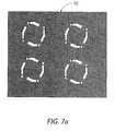
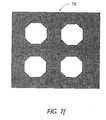
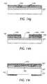
- FIG. 7 ashows a top view of a patterned mask used for processing.
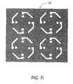
- FIG. 7 bshows a top view of a patterned mask used for processing.
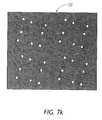
- FIG. 7 cshows a top view of a patterned mask used for processing.
- FIG. 7 dshows a top view of a patterned mask used for processing.
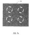
- FIG. 7 eshows a top view of a patterned mask used for processing.
- FIG. 7 fshows a top view of a patterned mask used for processing.
- FIG. 7 gshows a top view of a patterned mask used for processing.
- FIG. 7 hshows a top view of a patterned mask used for processing.
- FIG. 7 ishows a top view of a patterned mask used for processing.
- FIG. 7 jshows a top view of a patterned mask used for processing.
- FIG. 7 kshows a top view of a patterned mask used for processing.
- FIG. 7 lshows a top view of a patterned mask used for processing.
- FIG. 7 mshows a top view of a patterned mask used for processing.
- FIGS. 8 a - 8 oshow the processing steps in accordance with an embodiment of the invention.
- FIG. 9shows a top view of an embodiment in accordance with the invention.
- FIG. 10shows a side view of an embodiment in accordance with the invention.
- FIGS. 11 a - 11 kshow the processing steps in accordance with an embodiment of the invention.
- FIG. 12shows a top view of an embodiment in accordance with the invention.
- FIG. 13shows a side view of an embodiment in accordance with the invention.
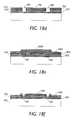
- FIGS. 14 a - 14 lshow the processing steps in accordance with an embodiment of the invention.
- FIG. 15shows a side view of an embodiment in accordance with the invention.
- FIGS. 16 a - 16 ishow the processing steps in accordance with an embodiment of the invention.
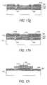
- FIGS. 17 a - 17 lshow the processing steps in accordance with an embodiment of the invention.
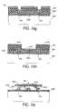
- FIGS. 18 a-mshow the processing steps in accordance with an embodiment of the invention.
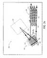
- FIG. 1shows an embodiment of optical cross-connect system 100 in accordance with the invention.
- Two dimensional array 104 of MEMS tilt mirrors 106is used to direct light beam 101 coming from two dimensional array 108 of optical fibers 110 to two dimensional array 112 of optical fibers 111 .
- Each mirror 106can rotate about two non-colinear axes in general.
- a typical diameter for mirror 106is in the range of 300 ⁇ m to 1000 ⁇ m.
- light beam 101 emerging from optical fiber 110is collimated using lenslet 115 typically having a diameter greater than about 50 ⁇ m and projected onto tilt mirror 106 which directs light beam 101 onto lenslet 116 which focuses light beam 101 into optical fiber 111 .
- light beam 101 coming from any one of optical fibers 110 in two dimensional array 108may be directed by one of mirrors 106 of two dimensional array 104 into selected optical fiber 111 of two dimensional optical fiber array 112 .
- the number of tilt mirrors 106is equal to the number of optical fibers 110 coming in which in turn is equal to the number of optical fibers 111 going out for optical cross-connect system 100 .
- FIG. 2 ashows optical cross-connect system 125 in accordance with the invention.
- Optical cross-connect system 125allows optical fibers 111 to be entered head-on by light beam 101 .
- Optical cross-connect system 125introduces two dimensional array 105 of tilt mirrors 107 to assure that light beam 101 enters optical fiber 111 head-on.
- Light beam 101 originating from optical fiber 110first strikes tilt mirror 106 and is reflected onto tilt mirror 107 which reflects light beam 101 head-on to optical fiber 111 .
- optical cross-connect system 125requires double the number of tilt mirrors that is required using optical cross-connect system 100 .
- the maximum mirror tilt angleis the maximal angular displacement required of mirror 106 or mirror 107 for addressing the most distant mirrors in array 105 or 104 , respectively.
- Typical maximum mirror tilt angles for this configuration assuming an optical path length of 8 cm given a beam radius of 180 ⁇ mare approximately 3.25° for two dimensional arrays 104 and 105 .
- FIG. 2 bshows an embodiment in accordance with the invention for an n ⁇ 1 optical switch for optical circuit switching.
- Light beam 101exits from one of optical fibers 110 in optical fiber array 108 to pass through lenslet array 115 for collimation and passing to tilt mirror array 104 to be reflected by tilt mirror 106 onto tilt mirror 177 which directs light beam 101 through lenslet 117 into desired one of optical fibers 114 .
- An application for an n ⁇ 1 optical switchis to multiplex a selectable subset of m different wavelengths from n (n ⁇ m) different optical fibers 110 in array 108 into desired one of optical fibers 114 .
- FIG. 2 cshows an embodiment in accordance with the invention for a 1 ⁇ n optical switch for optical circuit switching.
- Light beam 101exits from optical fiber 119 passing through lenslet 118 for collimation and being reflected by tilt mirror 177 onto desired tilt mirror 107 in tilt mirror array 105 .
- Tilt mirror 107reflects light beam 101 through lenslet array 116 for collimation and into desired one of optical fibers 111 in optical fiber array 112 .
- An application for a 1 ⁇ n optical switchis to route optical beam 101 from optical fiber 119 to any one of optical fibers 111 .
- Optical cross-connect system 150has two dimensional array 165 of tilt mirrors 106 and 107 and two dimensional array 155 consisting of incoming optical fibers 110 and outgoing optical fibers 112 .
- optical cross-connect system 150incorporates reflector 180 .
- Light beam 101leaves optical fiber 110 for collimation by lenslet 115 and is reflected off of tilt mirror 106 onto reflector 180 .
- From reflector 180light beam 101 is reflected off of tilt mirror 107 into lenslet 115 which focuses light beam 101 head-on into optical fiber 112 .
- Mirror shapecan be adjusted to be a circle, ellipse or polygon.
- mirror shapes that are ellipticalcan be used to capture the projection of a circular beam that is incident at an angle.
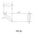
- FIG. 3 bshows circular beam 300 incident on ellipsoidal mirror 310 at angle ⁇ with respect to the rays of circular beam 300 .
- An optimum aspect ratio for ellipsoidal mirror 310can be derived from angle ⁇ .
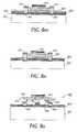
- FIG. 4 ashows the basic structure of tilt mirrors 106 and tilt mirrors 107 in accordance with an embodiment of the invention.
- Other geometriesare possible for the tilt mirror structure but the geometry of the alternatives to suspension arms 450 must allow for elongation of the tilt mirror structure between anchor points 440 . Otherwise the mirror structure cannot raise up after etching of the release layer.
- the surface of mirror 405 in FIG. 4 ais a substantially flat and stress free metal to allow precise optical pointing.
- Mirror 405is attached by flexure hinges 415 to suspension arms 450 .
- Suspension arms 450are typically made of nickel and provide clearance for rotation about axis 476 and 475 of mirror 405 by actuation of electrodes 410 .
- Mirror 405is raised automatically during a release etch described below and mirror 405 rotates slightly in its own plane as mirror 405 rises from substrate 499 (see FIG. 5 ).
- Typical heights for mirror 405 having a diameter of about 300 to 1000 ⁇ mis on the order of 20 to 100 ⁇ m.
- Electrodes 410 associated with four suspension arms 450may be individually charged to tilt mirror 405 about axis 475 and axis 476 with typical actuation voltages being about 10 to 50 volts.
- electrodes 410may extend under mirror structure 405 as shown in FIG. 4 a.
- Actuation electrodes 410may be actuated using either a DC or AC drive. If AC actuation is used the frequency of the AC drive needs to be significantly higher than the response time of the mechanical system being actuated. AC drive avoids potential buildup of electric charges in the dielectric materials between or close to actuation electrodes 410 .
- Actuation electrodes 410are beneficially driven with a bipolar signal, alternating between a positive voltage and an approximately equal negative voltage.
- the alternating waveformmay typically be square shaped sinusoidal, triangular or some other suitable shape as long as the rise and fall times are substantially shorter than the mechanical response time of tilt mirrors 106 and 107 , for example.
- a typical drive frequencywould be higher than 1 kHz if the mechanical resonance frequency of tilt mirrors 106 and 107 were on the order of 1 kHz. Since the actuation force is proportional to the square of the actuation voltage, the actuation force is independent of the sign of the voltage. The actuation force only varies during the transition from a voltage of one sign to a voltage of the opposite sign. Hence, the transition needs to be short compared to the resonance period of tilt mirrors 106 and 107 , for example.
- the bipolar signalreduces charge accumulation in the dielectric materials since the net charge accumulated in the dielectric material averages to approximately zero. With a DC signal for actuation there is the possibility of a net charge accumulation in the dielectric material over time which may act to screen or otherwise interfere with the applied actuation voltage.
- the basic structure shown in FIG. 4 a for tilt mirrors 106 and 107 in accordance with the inventionis based on stress-engineered metal films.
- Mirror 405 and flexure hinges 415are designed to be stress free while suspension arms 450 along the circumference of mirror 405 are made of a nickel having an MoCr layer with a built-in stress gradient deposited on them.
- Suspension arms 450are anchored to the substrate at anchor points 440 .
- Flexure hinges 415serve to attach mirror 405 to suspension arms 450 while isolating the stress and strain from mirror 405 to maintain planarity for optical pointing accuracy and providing the rotational flexibility about axis 477 that is needed for liftup and actuation.
- the actuation force for axis 475 and axis 476is created by the attraction between electrodes 410 situated the substrate and suspension arms 450 .
- electrodes 410underlie not only suspension arms 450 but are extended under each quadrant of mirror 405 as shown in FIG. 4 a to increase the total actuation force.
- limiting actuation electrodes 410 to the area underneath suspension arms 450provides a larger force per unit area as the actuation starts from near anchor point 440 where the initial separation between electrode 410 and suspension arms 450 is smallest and the separation then proceeds to decrease along the length of suspension arm 450 in a “zipper-like” fashion as suspension arm 450 is drawn toward electrode 410 .
- Two or more suspension arms 450may be used in the structure for tilt mirrors 106 and 107 with 4 (four) being typical. If mirror actuation is achieved by actuation of suspension arms 450 alone, a minimum of 3 (three) suspension arms 450 is required to allow tilt about two non-collinear axes.
- FIG. 4 bshows an embodiment in accordance with the invention of an actuatable mirror structure having 3 (three) suspension arms 450 . If mirror actuation about one tilt axis is achieved by having electrodes 410 extend under mirror 405 , it is possible to achieve tilting about two axes by having only 2 (two) suspension arms 450 .
- suspension arms 450 or suspension arms 455are deformable between anchor points 440 .
- the deformationis achieved by using suspension arms 450 that wrap around mirror 405 .
- the deformationis achieved through longitudinal flexures 456 in suspension arms 455 .
- Other embodiments allowing deformationwill be readily apparent to those of ordinary skill in the art.
- FIG. 5shows the basic structure of FIG. 4 a in cross-section, showing the placement of electrodes 410 underneath only suspension arms 450 .
- Optical path length(defined as the optical distance between exit face of incoming optical fiber bundle 108 and the entrance face of outgoing optical fiber bundle 112 ) effects a number of design parameters. Typical optical paths lie in the range of from about 5 cm-10 cm.
- a longer optical path for the embodiments shown in FIGS. 1-3is beneficial because it reduces the scan angle required of mirrors 106 and 107 to address optical fiber arrays 108 and 112 , respectively.
- a reduced scan anglein turn reduces the actuation voltage required for mirrors 106 and 107 to achieve a given resonance frequency or switching speed or results in a higher switching speed if the actuation voltage is kept the same.
- a reduced scan anglealso helps lower the mechanical stresses acting on the flexure elements such as flexure hinges 415 and longitudinal flexures 456 . Lowered mechanical stress reduces the potential problems of metal fatigue or hysteresis.
- collimating opticsneed to be positioned near the exit face of incoming optical fiber bundle 108 and the entrance face of outgoing optical fiber bundle 112 . This is typically done with lenslet arrays 115 and 116 but also with graded index (GRIN) collimators, ball lenses or other optical elements suitable for providing collimation. Collimation optics will always leave a finite residual divergence in the optical beam, for example, a commercially available GRIN fiber collimator typically leaves a residual divergence angle of from 0.1 to 0.25 degrees. The divergence angle combined with the optical path length determines the size required for mirrors 106 and 107 .
- GRINgraded index
- mirrors 106 and 107need to be larger than the maximum optical beam diameter. For a given divergence angle, a longer optical path requires larger mirrors 106 and 107 which results in larger mirror arrays 104 , 105 and 165 and a larger array pitch. A larger array pitch again requires a larger scan angle.
- Typical optical beam diameteris about 0.3 mm to 0.5 mm.
- the beam diameter after the collimation and expansion opticsoffers a degree of freedom in design. Expansion of the optical beam diameter relaxes the positional tolerances of all the optical elements which results in simplified packaging.
- the size required for mirrors 106 and 107is increased. Typical mirror diameters are typically on the order of 300 ⁇ m-1 mm. As mirror size increase it is more difficult to keep the mirror surface optically flat. Increasing mirror thickness enhances the ability to keep the mirror surface optically flat. A typical thickness for mirrors 106 and 107 lies in the range of 1-15 ⁇ m.
- FIG. 6 ashows a cross section of concave mirror 600 having radius of curvature R, diameter w, bow x, incoming collimated beam diameter d 0 , and diameter d 2 is the diameter of the reflected beam at optical path length L away from the surface of concave mirror 600 .
- Bow angle a ⁇ arctan (4x/w)is the divergence half angle due to bow x. Assuming that bow x is much less than radius of curvature R it can be shown that beam diameter d as a function of optical path length L is given approximately by:
- FIG. 6 bshows that beam diameter as a function of optical path length L for convex mirror 610 with optical path length L is given by:
- optical beam divergence arising from bow angle amust be kept small with respect to the optical beam divergence due to the residual collimation angle due to the collimation optics to maintain acceptable mirror size.
- mirror diameter wis 300 ⁇ m
- optical path length Lis 10 cm and d0 is 250 ⁇ m
- bow x of 10 nmis acceptable whereas bow x of 100 nm is not acceptable.
- Increasing mirror diameter w to 500 ⁇ mallows box x to be 100 nm.
- mirrors 106 and 107Larger thickness or diameters for mirrors 106 and 107 mean that mirrors 106 and 107 respond more slowly for a given actuation voltage for a fixed suspension stiffness and require a higher actuation voltage for a faster response at a higher suspension stiffness.
- electrodes 410can be tapered as a function of distance from anchor points 440 . A typical shape is then a triangular shape.
- Reducing width of actuation electrodes 410 along their lengthgradually reduces the actuation force at a fixed voltage as suspension arms 450 bend down towards actuation electrodes 410 .
- This reduction in actuation forceacts to offset the increased actuation force due to the gradually decreasing gap between suspension arm 450 and actuation electrode 410 .
- the decreasing gapis responsible for the onset of the instability.
- the mirror diameter, the required scan angle and the size of the instability region in combinationdetermine the minimum clearance from substrate 499 for mirrors 106 and 107 .
- Clearanceis adjusted by appropriate selection of the length of, for example, suspension arms 450 and the magnitude of the stress gradient that is introduced into suspension arms 450 .
- a typical clearance for mirrors 106 and 107is typically in the range of 20 ⁇ m to 200 ⁇ m from substrate 499 .
- the stiffness of the suspension system and the mass of mirrors 106 and 107determines the resonance frequency of mirrors 106 and 107 .
- the stiffness of the suspension systemis determined by the width, length, thickness and material of suspension arms 450 and flexural hinges 415 .
- a higher stiffnessresults in a higher resonance frequency with a resultant higher switching speed but requires higher actuation voltages.
- Higher stiffnessalso reduces the clearance of mirror 405 over substrate 499 for the same stress gradient and geometrical configuration.
- the ratio of the stiffness of suspension arm 450 to the stiffness of flexural hinge 415determines what fraction of the actuation force produces the tilt of mirror 405 versus the lowering of mirror 405 . Both tilt and lowering of mirror 405 will be present. Hence, it is desirable that the stiffness of flexural hinges 415 is less than the stiffness of suspension arms 450 .
- Two dimensional micro-mirror arrayssuch as two dimensional array 104 of MEMS tilt mirrors 106 may be fabricated in a number of ways in accordance with the invention.
- Various substratesmay be used such as, for example, glass, bulk silicon, and silicon on insulator.
- FIGS. 7 a - 7 fare exemplary and shown for a two by two micro-mirror array but may be adapted to an arbitrary micro-mirror array size or to a single mirror structure.
- FIGS. 8 a - 8 oshow the fabrication steps for two dimensional array 104 of MEMS tilt mirrors 106 using glass as the substrate in accordance with an embodiment of the invention.
- FIGS. 8 a - 8 oare cross-sectional views taken substantially along line 8 — 8 in FIG. 9 .
- High quality unannealed glass substrate 801is cleaned prior to application of photoresist lift-off mask 701 .
- lift-off mask 701is patterned as shown in FIG.
- FIG. 8 bshows removal of photoresist lift-off mask 701 and the portion of chromium layer 813 overlying photoresist lift-off mask 701 using an acetone soak and leaving actuation electrodes 410 (see FIG. 4) and anchor points 440 in place.
- Si 3 N 4 layer 803having a typical thickness of about 150 nm is deposited over glass substrate 801 , over actuation electrodes 410 (see FIG. 4) and anchor points 440 as shown in FIG. 8 c.
- amorphous silicon layer 804is LPCVD deposited over Si 3 N 4 layer 803 to a typical thickness of about 500 nm.
- Photoresist mask 702is applied over amorphous silicon layer 804 and patterned as shown in FIG. 7 b.
- Vias 890are dry etched using an O 2 /SF 6 plasma down to anchor points 440 and electrical contacts (not shown).
- copper seed layer 805is deposited to a typical thickness of about 200 nm over amorphous silicon layer 804 , electrical contacts (not shown) and anchor points 440 as shown in FIG. 8 e.
- FIG. 8 fshows electroplating mask 703 applied over copper layer 805 and patterned as shown in FIG. 7 c in preparation for electroplating of nickel layer 806 .
- Nickel layer 806is electroplated over copper layer 805 to a typical thickness of about 1 ⁇ m as shown in FIG. 8 g.
- Nickel layer 806functions as a structural support layer for mirror 405 and suspension arms 450 (see FIGS. 4 and 9 ).
- Electroplating mask 703is then removed.
- Electroplating mask 704is applied and patterned as shown in FIG. 7 d where only the area for mirror 405 is left exposed.
- Electroplating mask 704is the mask for the nickel electroplating of mirror 405 to a typical thickness of about 2-3 ⁇ m as shown in FIG. 8 h.
- Photoresist layer 704is removed to produce the structure shown in FIG. 8 i.
- MoCr photoresist lift-off mask 705is applied over mirror 405 and copper layer 805 as shown in FIG. 8 j.
- Lift-off mask 705is patterned as shown in FIG. 7 e and then MoCr layer 810 is sputter deposited over lift-off mask 705 .
- Typical sputter parameters for deposition of MoCr layer 810are shown in Table 1 below and result in an internal stress gradient of about 3.0 Gpa across MoCr layer 810 .
- Total liftcan be designed using conventional micro-spring recipes such as disclosed in U. S. Pat. No. 5,914,218 which is incorporated by reference.
- An acetone soakis performed to remove lift-off mask 705 and portions of MoCr layer 810 overlying lift-off mask 705 resulting in the structure shown in FIG. 8 k.
- Photoresist lift-off mask 706is applied over exposed copper layer 805 , exposed nickel layer 806 and remaining portion of MoCr layer 810 .
- Lift-off mask 706is patterned as shown in FIG. 7 f to expose only the surface of mirror 405 .
- Gold layer 815is then sputter deposited to coat mirror 405 with gold.
- lift-off mask 706 along with the portion of gold layer 815 overlying lift-off mask 706is removed using an acetone soak. The resulting structure is shown in FIG. 8 m.
- exposed copper layer 805is removed using an alkaline etch, typically a mix of 5H 2 O:5NH 4 OH:H 2 O 2 . This etch avoids damaging the exposed nickel.
- FIG. 8 nis released using xenon difluoride (XeF 2 ) which removes sacrificial amorphous silicon layer 804 .
- XeF 2xenon difluoride
- remainder of copper layer 805remains attached to structure 899 .
- Removal of amorphous silicon layer 804causes release of structure 899 as shown in FIG. 8 o.
- Structure 899raises up from substrate 801 due to the internal stress gradient in MoCr layer 810 . Since MoCr layer 810 is the surface layer for suspension arms 450 (see also FIG. 4 ), the internal stress gradient in MoCr layer 810 acts to force up all four of suspension arms 450 , thereby raising mirror 405 .
- FIG. 10shows a partial cut-away view of MEMS tilt mirror 106 on glass substrate 801 .
- FIG. 10shows a partial cut-away view of MEMS tilt mirror 106 on glass substrate 801 and showing optical beams 1010 and 1020 .
- Optical beam 1020reaches mirror 405 by passing through glass substrate 801 .
- FIGS. 11 a - 11 kshow the fabrication steps for two dimensional array 104 of MEMS tilt mirrors 106 using bulk silicon as the substrate in accordance with an embodiment of the invention.
- Typical thickness for bulk silicon substrate 1101is on the order of 100 ⁇ m to facilitate etching.
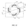
- FIGS. 11 a - 11 kare cross-sectional views along line 12 — 12 in FIG. 12 .
- FIG. 11 ashows bulk silicon substrate 1101 with dielectric, typically Si 3 N 4 , layers 1102 and 1103 deposited on two sides of bulk silicon substrate 1101 .
- Photoresist lift-off mask 709is applied over dielectric layer 1103 and patterned as shown in FIG. 7 i.
- Cr layer 1105is then sputter deposited over lift-off mask 709 and exposed dielectric layer 1103 . Subsequently, lift-off mask 709 and overlying portions of Cr layer 1105 are removed using an acetone soak.
- FIG. 11 bshows the deposition of dielectric layer 1111 over electrodes 410 to electrically isolate electrodes 410 .
- Dielectric layer 1111may be Si 3 N 4 or another dielectric material.
- SiO 2 layer 1106is deposited over dielectric layer 1111 for release purposes.
- FIG. 11 cshows photoresist mask layer 711 applied over SiO 2 layer 1106 and then patterned as shown in FIG. 7 k. Exposed portions of dielectric layer 1111 and SiO 2 layer 1106 are then dry etched away.
- Photoresist lift-off mask layer 710is applied in FIG. 11 d and patterned as shown in FIG. 7 j.
- MoCr layer 1108is sputter deposited to a typical thickness of about 500 nm over mask layer 710 as detailed in Table 1 above.
- Photoresist lift-off mask 710 and overlying portions of MoCr layer 1108are removed using an acetone soak to achieve the structure in FIG. 11 f.
- FIG. 11 gshows photoresist lift-off mask layer 708 applied over dielectric layer 1106 and MoCr layer 1108 and then patterned as shown in FIG. 7 h.
- Gold layer 1109is sputter deposited over photoresist lift-off mask layer 708 to a typical thickness of about 100 nm.
- Photolift-off mask layer 708 along with overlying portions of gold layer 1109are then removed using an acetone soak.
- the entire top of the structureis covered with photoresist layer 1110 to a thickness of about 5-10 ⁇ m as shown in FIG. 11 h and hard baked for about 20 minutes at approximately 120° C. to protect the top of the structure against subsequent processing steps.
- photoresist mask 707is applied to dielectric layer 1102 and patterned as shown in FIG. 7 g.
- Photoresist mask 707exposes the areas for the deep reactive ion etch (DRIE) which removes the exposed sections of dielectric layer 1102 and overlying bulk silicon substrate 1101 , dielectric layer 1103 and dielectric layer 1106 to form suspended mirror 405 .
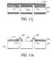
- FIG. 11 jshows the extent of the deep reactive ion etch.
- MoCr suspension arms 450are also released from dielectric layer 1106 .
- photoresist mask layers 707 and 1110are removed using either a dry etch or an acetone soak followed by an etch in a photoresist stripper.
- Finished MEMS tilt mirror structureis shown in FIG. 13 where arrows 1310 and 1320 indicate that the bottom as well as the top surface of mirror 405 may be used to reflect light if minor changes are made to the processing steps 11 a - 11 j so that the bottom of mirror 405 is also coated with gold.
- FIGS. 14 a - 14 lshow the fabrication steps for two dimensional array 104 of MEMS tilt mirrors 106 using a silicon on insulator substrate in accordance with an embodiment of the invention.
- FIGS. 14 a - 14 lare cross-sectional views along line 12 — 12 in FIG. 12 .
- FIG. 14 ashows silicon on insulator substrate 1401 with dielectric, typically Si 3 N 4 , layers 1402 and 1403 deposited on two sides of silicon on insulator substrate 1401 .
- Photoresist lift-off mask 709is applied over dielectric layer 1403 and patterned as shown in FIG. 7 i.
- Cr layer 1405is sputter deposited to a typical thickness of about 100 nm over patterned photoresist lift-off mask 709 .
- Photoresist lift-off mask 709 and overlying portions of Cr layer 1405are removed using an acetone soak or other standard lift-off technique as shown in FIG. 14 b .
- dielectric layer 1411is deposited over actuator electrodes 410 to electrically isolate electrodes 410 .
- Dielectric layer 1411may be Si 3 N 4 or another dielectric material.
- porous SiO 2 layer 1406is deposited over dielectric layer 1411 for release purposes.
- FIG. 14 dshows photoresist mask layer 711 applied over SiO 2 layer 1406 and then patterned as shown in FIG. 7 k. Exposed portions of SiO 2 layer 1406 and underlying portions of dielectric layer 1411 are then dry etched away.
- Photoresist lift-off mask layer 710is applied over remaining portions of SiO 2 layer 1406 and exposed portions of layer 141 in FIG. 14 e and patterned as shown in FIG. 7 j. As shown in FIG. 14 f , MoCr layer 1408 is sputter deposited to a typical thickness of about 500 nm over mask layer 710 as detailed in Table 1 above.
- Photoresist lift-off mask 710 and overlying portions of MoCr layer 1408are removed using an acetone soak or other lift-off technique to achieve the structure shown in FIG. 14 g.
- FIG. 14 hshows photoresist lift-off mask 708 applied over dielectric layer 1406 and MoCr layer 1408 and then patterned as shown in FIG. 7 h.
- Gold layer 1409is sputter deposited over photoresist lift-off mask layer 708 to a typical thickness of about 100 nm.
- Photoresist lift-off mask layer 708 along with overlying portions of gold layer 1409are then removed using an acetone soak or other lift-off technique.
- photoresist layer 1410to a thickness of about 5-10 nm as shown in FIG. 14 i and hard baked for about 20 minutes at 120° C. to act as protection for subsequent processing steps.
- Photoresist mask layer 713is applied over dielectric layer 1402 and patterned as shown in FIG. 7 m. The exposed portion of dielectric layer 1402 is removed using a buffered hydrofluoric acid etch to allow for the following potassium hydroxide etch. Photoresist mask layer 713 is then also removed using an acetone soak.
- Silicon on insulator substrate 1401is backside etched using a 45% potassium hydroxide solution at a temperature of approximately 60° C. until buried oxide layer 1475 is reached as shown in FIG. 14 j. Buried oxide layer 1475 functions as an etch stop. Remaining portion of dielectric layer 1402 and exposed portion of buried dielectric layer 1475 are coated with photoresist mask 707 which is patterned as shown in FIG. 7 g. Exposed sidewalls in cavity 1450 are also coated with photoresist layer 1451 .
- the exposed areasare then deep reactive ion etched to remove the exposed portion of buried dielectric layer 1475 as well as the portions of silicon on insulator substrate 1401 , dielectric layer 1403 and dielectric layer 1406 that lie over exposed portion of buried dielectric layer 1475 .
- the resultant structureis shown in FIG. 14 k.
- photoresist mask layers 707 along with photoresist layers 1410 and 1451are removed using either a dry etch or an acetone soak followed by an etch in a photoresist stripper.
- Finished MEMS tilt mirror structure 1500is shown in FIG. 15 where arrows 1510 and 1520 indicate that the bottom as well as the top surface of mirror 405 may be used to reflect light if minor changes are made to the processing steps 14 a - 14 l so that the bottom of mirror 405 is coated with gold.
- FIGS. 16 a - 16 ishow the fabrication steps for two dimensional array 104 of MEMS tilt mirrors 106 using any one of the previously mentioned substrates by using polysilicon as the mechanical mirror material in accordance with an embodiment of the invention.
- FIGS. 16 a - 16 iare cross-sectional views along line 9 — 9 in FIG. 9 .
- FIG. 16 ashows application of photoresist lift-off mask layer 701 on substrate 1601 . After application, lift-off mask layer 701 is patterned as shown in FIG. 7 a for anchor points 440 , actuation electrodes 410 and electrical contacts (not shown). Cr layer 1613 is deposited over lift-off mask layer 701 to a typical thickness of about 100 nm.
- FIG. 16 ashows application of photoresist lift-off mask layer 701 on substrate 1601 .
- lift-off mask layer 701is patterned as shown in FIG. 7 a for anchor points 440 , actuation electrodes 410 and electrical contacts (not shown).
- FIG. 16 bshows removal of photoresist lift-off mask layer 701 and the portion of Cr layer 1613 overlying photoresist lift-off mask 701 using an acetone soak or other lift-off technique leaving actuation electrodes 410 (see FIG. 4) and anchor points 440 in place.
- LPCVDLow Pressure Chemical Vapor Deposition
- Si 3 N 4 layer 1603is deposited to a typical thickness of about 200 nm over substrate 1601 , anchor points 440 and actuation electrodes 410 (see FIG. 4) followed by deposition of porous SiO 2 layer 1604 over Si 3 N 4 layer 1603 to a typical thickness of about 150 nm as shown in FIG. 16 c.
- photoresist mask layer 702is applied to SiO 2 layer 1604 and patterned as shown in FIG. 7 b. Vias 1690 are dry etched using an O 2 /SF 6 plasma down to anchor points 440 and electrical contacts (not shown). After removal of photoresist mask layer 702 using an acetone soak, polysilicon layer 1605 is deposited to a typical depth of about 6 ⁇ m to act as the mechanical layer for mirror 405 . Then a chemical mechanical polish is applied to polysilicon layer 1605 to planarize the top surface of polysilicon layer 1605 resulting in the structure shown in FIG. 16 e.
- Photoresist mask layer 1611is applied over polysilicon layer 1605 and patterned as the photo negative of photoresist mask 703 shown in FIG. 7 c. Exposed portions of polysilicon layer 1605 are then dry etched away giving the structure in FIG. 16 f. Photoresist mask layer 1611 is then removed using either an acetone soak or a dry etch. Photoresist lift-off mask layer 705 is then deposited over exposed SiO 2 layer 1604 and remaining polysilicon layer 1605 . With reference to FIG. 16 g, photoresist lift-off mask layer 705 is patterned as shown in FIG.
- MoCr layer 1610is sputter deposited to a typical thickness of about 500 nm on photoresist lift-off mask layer 705 and on exposed portions of polysilicon layer 1605 as described in Table 1. Photoresist lift-off mask layer 705 and overlying portions of MoCr layer 1610 are then removed using an acetone soak or other lift-off technique.
- Photoresist lift-off mask layer 704is applied over polysilicon layer 1605 and exposed portion of SiO 2 layer 1604 and patterned as shown in FIG. 7 f.
- Gold layer 1615is sputter deposited to a typical thickness of about 100 nm on photoresist lift-off mask 706 as shown in FIG. 16 h.
- photoresist lift-off mask 706 and overlying gold layer 1615is removed using an acetone soak or other lift-off technique leaving gold layer 1615 on mirror 405 .
- a wet etchis performed on porous SiO 2 layer using forty nine percent hydrofluoric acid for about 15 minutes to release mirror 405 as shown in FIG. 16 i.
- the resulting structureis similar to that shown in the partial cutaway of FIG. 10 .
- Tilt mirror 106 flatnesscan be achieved by making tilt mirrors 106 from two adjacent stress metal layers with opposite stress gradients.
- FIGS. 17 a - 17 lshow the fabrication steps for two dimensional array 104 of MEMS tilt mirrors 106 using glass as the substrate in accordance with an embodiment of the invention to produce opposing stress.
- FIGS. 17 a - 17 mare cross-sectional views taken substantially along line 8 — 8 in FIG. 9 .
- High quality unannealed glass substrate 801is cleaned prior to application of photoresist lift-off mask 701 . After application, lift-off mask 701 is patterned as shown in FIG. 17 a for anchor points 440 , actuation electrodes 410 and electrical contacts (not shown).
- FIG. 17 bshows removal of photoresist lift-off mask 701 and the portion of chromium layer 813 overlying photoresist lift-off mask 701 using an acetone soak and leaving actuation electrodes 410 (see FIG. 4) and anchor points 440 in place.
- Si 3 N 4 layer 803having a typical thickness of about 150 nm is deposited over glass substrate 801 , over actuation electrodes 410 (see FIG. 4) and anchor points 440 as shown in FIG. 17 c.
- amorphous silicon layer 804is LPCVD deposited over Si 3 N 4 layer 803 to a typical thickness of about 500 nm.
- Photoresist mask 702is applied over amorphous silicon layer 804 and patterned as shown in FIG. 7 b .
- Vias 890are dry etched using an O 2 /SF 6 plasma down to anchor points 440 and electrical contacts (not shown).
- titanium adhesion layer 1701is deposited to a typical thickness of about 50 nm over amorphous silicon layer 804 , electrical contacts (not shown) and anchor points 440 and followed by deposition of gold reflective layer 1705 over titanium adhesion layer 1701 as shown in FIG. 17 e.
- FIG. 17 fshows lift-off mask 703 applied over gold reflective layer 1705 and patterned as shown in FIG. 7 c in preparation for deposition of MoCr layer 1710 .
- FIG. 17 gshows sputter deposition of five sublayers of MoCr, resulting in a typical total MoCr layer 1712 thickness of 1 ⁇ m. Typical sputter parameters for deposition of MoCr layer 1712 are shown in Table 1 above and result in MoCr layer 1712 having an internal stress gradient of about 3.0 Gpa.
- Photoresist lift-off mask 704is applied over MoCr layer 1712 .
- Lift-off mask 704is patterned as shown in FIG. 7 d leaving only the mirror area exposed.
- MoCr layer 1714is sputter deposited over lift-off mask 704 with a designed in stress gradient opposite to that of MoCr layer 1712 as shown in FIG. 17 h. This results in substantially zero net force in mirror 405 .
- An acetone soakis performed to remove lift-off mask 704 and portions of MoCr layer 1714 overlying lift-off mask 704 .
- Exposed portion of gold reflective layer 1705is removed using TRANSENE gold etchant followed by a mixture of HF:H 2 O to remove the exposed portion of titanium adhesion layer 1712 as shown in FIG. 17 i.
- Photoresist lift-off mask 706is applied over remaining portion of MoCr layer 1714 and exposed portion of MoCr layer 1712 .
- Lift-off mask 706is patterned as shown in FIG. 7 f to expose only the surface of mirror 405 .
- Gold layer 815is then sputter deposited to coat mirror 405 with gold as shown in FIG. 17 j.
- lift-off mask 706 along with the portion of gold layer 815 overlying lift-off mask 706is removed using an acetone soak. The resulting structure is shown in FIG. 17 k. Finally, the structure shown in FIG.
- 17 lis released using xenon difluoride (XeF 2 ) which removes sacrificial amorphous silicon layer 804 . Removal of amorphous silicon layer 804 causes release of structure 1750 . Structure 1750 raises up from substrate 801 due to the internal stress gradient in MoCr layer 1712 . Since MoCr layer 1712 forms suspension arms 450 (see also FIG. 4 ), the internal stress gradient in MoCr layer 1712 acts to force up all four of suspension arms 450 , thereby raising mirror 405 .
- XeF 2xenon difluoride
- Tilt mirror 106 flatnesscan also be achieved by making tilt mirrors 106 from two adjacent stress polysilicon layers with opposite stress gradients.
- Polysiliconcan be stressed by adjusting deposition temperature (as opposed to pressure for MoCr) during LPCVD. Stresses on the order of 500 mPa can be readily achieved as has been shown by Arthur Heuer of Case Western Reserve University.
- FIGS. 18 a - 18 mshow the fabrication steps for MEMS tilt mirrors 106 using glass as the substrate in accordance with an embodiment of the invention to produce opposing stress.
- FIGS. 18 a - 18 mare cross-sectional views taken substantially along line 8 — 8 in FIG. 9 .
- High quality unannealed glass substrate 801is cleaned prior to application of photoresist lift-off mask 701 .
- lift-off mask 701is patterned as shown in FIG. 18 a for anchor points 440 , actuation electrodes 410 and electrical contacts (not shown).
- 100 nm of chromium 813is sputter deposited over lift-off mask 701 .
- FIG. 18 bshows removal of photoresist lift-off mask 701 and the portion of chromium layer 813 overlying photoresist lift-off mask 701 using an acetone soak and leaving actuation electrodes 410 (see FIG. 4) and anchor points 440 in place.
- Si 3 N 4 layer 803having a typical thickness of about 150 nm is deposited over glass substrate 801 , over actuation electrodes 410 (see FIG. 4) and anchor points 440 as shown in FIG. 18 c.
- amorphous silicon layer 804is LPCVD deposited over Si 3 N 4 layer 803 to a typical thickness of about 500 nm. Then Si 3 N 4 layer 1803 is LPCVD deposited over amorphous silicon layer 804 to serve as a first insulation layer against XeF 2 for the polysilicon structure to be deposited later.
- Photoresist mask 702is applied over layer Si 3 N 4 layer 1803 and patterned as shown in FIG. 7 b. Vias 890 are dry etched using an O 2 /SF 6 plasma down to anchor points 440 and electrical contacts (not shown).
- stressed polysilicon layer 1804is deposited using LPCVD and photoresist layer 2004 is applied over polysilicon layer 1804 and patterned as the inverse of mask 703 as shown in FIG. 7 c. Exposed portion of polysilicon layer 1804 is dry etched in an O 2 /SF 6 plasma etcher and photoresist layer 2004 is removed resulting in the structure shown in FIG. 18 f.
- Photoresist layer 2005is applied over polysilicon layer 1804 and patterned as the inverse of mask 703 shown in FIG. 7 c but slightly optically magnified to produce an approximately 1 ⁇ m overhang. Then a timed wet etch using an HF solution is performed of exposed Si 3 N 4 layer 1803 as shown in FIG. 18 g. Photoresist layer 2004 is then removed using an acetone soak. Si 3 N 4 layer 1809 is deposited to encapsulate polysilicon layer 1804 . As shown in FIG. 18 h, photoresist mask 704 is deposited over Si 3 N 4 layer 1809 and patterned as shown in FIG. 7 d to expose the mirror region. Si 3 N 4 layer 1809 is then etched using an HF etchant.
- polysilicon layer 1805is deposited with a stress gradient opposite to polysilicon layer 1804 .
- photoresist layer 2006is then applied over polysilicon layer 1805 and patterned to be the inverse of mask 704 shown in FIG. 7 d .
- Exposed portions of polysilicon layer 1805are then dry etched, stopping on Si 3 N 4 layer 1809 .
- Photoresist layer 2006is then removed using an acetone soak.
- photoresist layer 2007is applied over polysilicon layer 1805 and over exposed Si 3 N 4 layer 1809 and patterned as the inverse of photomask 703 shown in FIG. 7 c.
- Exposed Si 3 N 4 layer 1809is then etched away as shown in FIG. 18 j.
- Photoresist layer 2007is then removed using an acetone soak.
- Photoresist mask 704is applied over exposed portions of polysilicon layer 1805 , amorphous silicon layer 804 and Si 3 N 4 layer 1809 and patterned as shown in FIG. 7 d.
- Gold layer 1825is then deposited over photoresist mask 704 as shown in FIG. 18 k.
- photoresist mask 704is removed using a liftoff process to leave the structure shown in FIG. 18 l .
- the structure shown in FIG. 17 mis released using xenon difluoride (XeF 2 ) which removes sacrificial amorphous silicon layer 804 .
- XeF 2xenon difluoride
- Structure 1850raises up from substrate 801 due to the internal stress gradient in polysilicon layer 1803 . Since polysilicon layer 1803 forms suspension arms 450 (see also FIG. 4 ), the internal stress gradient in polysilicon layer 1803 acts to force up all four of suspension arms 450 , thereby raising mirror 405 .
Landscapes
- Physics & Mathematics (AREA)
- General Physics & Mathematics (AREA)
- Optics & Photonics (AREA)
- Mechanical Light Control Or Optical Switches (AREA)
- Micromachines (AREA)
Abstract
Description
| TABLE 1 | |||
| Sputter Deposition Conditions | Time (sec) | ||
| Pressure: 1.6 mT | 390 | ||
| Voltage: 518 volts | |||
| Current: 1.13 A | |||
| Pressure: 2.2 mT | 330 | ||
| Voltage: 470 volts | |||
| Current: 1.26 A | |||
| Pressure: 3.0 | 300 | ||
| Voltage: 457 volts | |||
| Current: 1.30 A | |||
| Pressure: 3.9 mT | 330 | ||
| Voltage: 453 volts | |||
| Current: 1.31 A | |||
| Pressure: 5.0 | 300 | ||
| Voltage: 457 volts | |||
| Current: 1.30 A | |||
Claims (15)
Priority Applications (4)
| Application Number | Priority Date | Filing Date | Title |
|---|---|---|---|
| US09/672,380US6300665B1 (en) | 2000-09-28 | 2000-09-28 | Structure for an optical switch on a silicon on insulator substrate |
| EP01307608AEP1193526B1 (en) | 2000-09-28 | 2001-09-07 | Mirror structure |
| DE60107518TDE60107518T2 (en) | 2000-09-28 | 2001-09-07 | mirror structure |
| JP2001286788AJP4920844B2 (en) | 2000-09-28 | 2001-09-20 | Structure of optical switch on silicon substrate on insulator and method of manufacturing the same |
Applications Claiming Priority (1)
| Application Number | Priority Date | Filing Date | Title |
|---|---|---|---|
| US09/672,380US6300665B1 (en) | 2000-09-28 | 2000-09-28 | Structure for an optical switch on a silicon on insulator substrate |
Publications (1)
| Publication Number | Publication Date |
|---|---|
| US6300665B1true US6300665B1 (en) | 2001-10-09 |
Family
ID=24698303
Family Applications (1)
| Application Number | Title | Priority Date | Filing Date |
|---|---|---|---|
| US09/672,380Expired - LifetimeUS6300665B1 (en) | 2000-09-28 | 2000-09-28 | Structure for an optical switch on a silicon on insulator substrate |
Country Status (4)
| Country | Link |
|---|---|
| US (1) | US6300665B1 (en) |
| EP (1) | EP1193526B1 (en) |
| JP (1) | JP4920844B2 (en) |
| DE (1) | DE60107518T2 (en) |
Cited By (53)
| Publication number | Priority date | Publication date | Assignee | Title |
|---|---|---|---|---|
| US6362556B1 (en)* | 1999-03-30 | 2002-03-26 | Agilent Technologies, Inc. | Electrically actuated optical switch having a surface pivotable Mirror |
| US6394617B1 (en)* | 2000-12-29 | 2002-05-28 | Avanex Corporation | Method and apparatus for latched bimorph optical switchs |
| US6430333B1 (en)* | 1999-04-15 | 2002-08-06 | Solus Micro Technologies, Inc. | Monolithic 2D optical switch and method of fabrication |
| US6466356B1 (en)* | 2000-09-28 | 2002-10-15 | Xerox Corporation | Structure for an optical switch on a silicon substrate |
| US20020176658A1 (en)* | 2000-10-13 | 2002-11-28 | John Prohaska | Re-configurable wavelength and dispersion selective device |
| US6490384B2 (en)* | 2001-04-04 | 2002-12-03 | Yoon-Joong Yong | Light modulating system using deformable mirror arrays |
| US6501588B1 (en)* | 2000-09-28 | 2002-12-31 | Xerox Corporation | Method for an optical switch on a silicon substrate |
| US6504643B1 (en)* | 2000-09-28 | 2003-01-07 | Xerox Corporation | Structure for an optical switch on a substrate |
| US6545385B2 (en)* | 2000-04-11 | 2003-04-08 | Sandia Corporation | Microelectromechanical apparatus for elevating and tilting a platform |
| US6603894B1 (en)* | 2001-01-26 | 2003-08-05 | Tellium, Inc. | MEMS mirror arrays and external lens system in an optical switch |
| US6632373B1 (en)* | 2000-09-28 | 2003-10-14 | Xerox Corporation | Method for an optical switch on a substrate |
| US6632374B1 (en)* | 2000-09-28 | 2003-10-14 | Xerox Corporation | Method for an optical switch on a silicon on insulator substrate |
| US20030202738A1 (en)* | 2002-04-30 | 2003-10-30 | Xerox Corporation | Optical switching system |
| US20040023430A1 (en)* | 2002-07-16 | 2004-02-05 | Gormley Colin Stephen | Method for forming a micro-mechanical component in a semiconductor wafer, and a semiconductor wafer comprising a micro-mechanical component formed therein |
| US6753638B2 (en) | 2000-02-03 | 2004-06-22 | Calient Networks, Inc. | Electrostatic actuator for micromechanical systems |
| US6785038B2 (en)* | 2001-01-17 | 2004-08-31 | Optical Coating Laboratory, Inc. | Optical cross-connect with magnetic micro-electro-mechanical actuator cells |
| US20040202407A1 (en)* | 2003-04-07 | 2004-10-14 | Hoke Charles D. | Closed loop alignment system for fiber optic cross-connect switches |
| US6825967B1 (en) | 2000-09-29 | 2004-11-30 | Calient Networks, Inc. | Shaped electrodes for micro-electro-mechanical-system (MEMS) devices to improve actuator performance and methods for fabricating the same |
| US20050008074A1 (en)* | 2003-06-25 | 2005-01-13 | Van Beek Petrus J.L. | Wireless video transmission system |
| US20050025413A1 (en)* | 2003-07-11 | 2005-02-03 | Kenichiro Takahashi | Optical device control apparatus and optical device control method |
| US6891240B2 (en) | 2002-04-30 | 2005-05-10 | Xerox Corporation | Electrode design and positioning for controlled movement of a moveable electrode and associated support structure |
| US6912078B2 (en) | 2001-03-16 | 2005-06-28 | Corning Incorporated | Electrostatically actuated micro-electro-mechanical devices and method of manufacture |
| US6960849B1 (en) | 2003-03-31 | 2005-11-01 | Sandia Corporation | Three-dimensional microelectromechanical tilting platform operated by gear-driven racks |
| US20060087064A1 (en)* | 2004-10-27 | 2006-04-27 | Palo Alto Research Center Incorporated | Oblique parts or surfaces |
| US20060095943A1 (en)* | 2004-10-30 | 2006-05-04 | Demircin Mehmet U | Packet scheduling for video transmission with sender queue control |
| US20060095942A1 (en)* | 2004-10-30 | 2006-05-04 | Van Beek Petrus J | Wireless video transmission system |
| US7046411B1 (en) | 2005-04-29 | 2006-05-16 | Sandia Corporation | Tensile-stressed microelectromechanical apparatus and micromirrors formed therefrom |
| US20060261436A1 (en)* | 2005-05-19 | 2006-11-23 | Freescale Semiconductor, Inc. | Electronic device including a trench field isolation region and a process for forming the same |
| US7159397B1 (en) | 2005-06-07 | 2007-01-09 | Sandia Corporation | Tensile-stressed microelectromechanical apparatus and tiltable micromirrors formed therefrom |
| US20070067480A1 (en)* | 2005-09-19 | 2007-03-22 | Sharp Laboratories Of America, Inc. | Adaptive media playout by server media processing for robust streaming |
| US20070148895A1 (en)* | 2005-12-28 | 2007-06-28 | Palo Alto Research Center Incorporated | Integrateable capacitors and microcoils and methods of making thereof |
| US20070145523A1 (en)* | 2005-12-28 | 2007-06-28 | Palo Alto Research Center Incorporated | Integrateable capacitors and microcoils and methods of making thereof |
| US20070153916A1 (en)* | 2005-12-30 | 2007-07-05 | Sharp Laboratories Of America, Inc. | Wireless video transmission system |
| US20070236599A1 (en)* | 2006-03-31 | 2007-10-11 | Sharp Laboratories Of America, Inc. | Accelerated media coding for robust low-delay video streaming over time-varying and bandwidth limited channels |
| CN100356566C (en)* | 2002-09-19 | 2007-12-19 | 日本电信电话株式会社 | Semiconductor device with micro electromechanical system |
| US20080069201A1 (en)* | 2006-09-18 | 2008-03-20 | Sharp Laboratories Of America, Inc. | Distributed channel time allocation for video streaming over wireless networks |
| US20080107173A1 (en)* | 2006-11-03 | 2008-05-08 | Sharp Laboratories Of America, Inc. | Multi-stream pro-active rate adaptation for robust video transmission |
| GB2445107A (en)* | 2006-12-20 | 2008-06-25 | Boeing Co | Optical cross-connect switch with wedge spacer which supports two parallel one-dimensional arrays of optical fibres |
| US20080291524A1 (en)* | 2003-11-01 | 2008-11-27 | Fusao Ishil | Mirror device |
| US7491622B2 (en) | 2006-04-24 | 2009-02-17 | Freescale Semiconductor, Inc. | Process of forming an electronic device including a layer formed using an inductively coupled plasma |
| US7528078B2 (en) | 2006-05-12 | 2009-05-05 | Freescale Semiconductor, Inc. | Process of forming electronic device including a densified nitride layer adjacent to an opening within a semiconductor layer |
| US7670895B2 (en) | 2006-04-24 | 2010-03-02 | Freescale Semiconductor, Inc | Process of forming an electronic device including a semiconductor layer and another layer adjacent to an opening within the semiconductor layer |
| US7784076B2 (en) | 2004-10-30 | 2010-08-24 | Sharp Laboratories Of America, Inc. | Sender-side bandwidth estimation for video transmission with receiver packet buffer |
| US20110188017A1 (en)* | 2008-10-08 | 2011-08-04 | Carl Zeiss Smt Gmbh | Methods and devices for driving micromirrors |
| US8018850B2 (en) | 2004-02-23 | 2011-09-13 | Sharp Laboratories Of America, Inc. | Wireless video transmission system |
| US20110261431A1 (en)* | 2010-04-22 | 2011-10-27 | Holger Conrad | Micromechanical element |
| US20110273694A1 (en)* | 2009-01-09 | 2011-11-10 | Carl Zeiss Smt Gmbh | Individual mirror for constructing a faceted mirror, in particular for use in a projection exposure system for microlithography |
| US9325998B2 (en) | 2003-09-30 | 2016-04-26 | Sharp Laboratories Of America, Inc. | Wireless video transmission system |
| US20160139340A1 (en)* | 2013-06-27 | 2016-05-19 | Oplink Communications, Inc. | Mems fiber optical switch |
| US20190025573A1 (en)* | 2016-04-01 | 2019-01-24 | Intel Corporation | Piezo actuators for optical beam steering applications |
| US12130423B1 (en) | 2020-08-12 | 2024-10-29 | Bae Systems Space & Mission Systems Inc. | Two degree-of freedom reactionless pointing and scanning system |
| US12313905B1 (en) | 2022-03-15 | 2025-05-27 | Bae Systems Space & Mission Systems Inc. | Monolithic two-axis flexure with center hole feature |
| US12320466B2 (en) | 2021-03-10 | 2025-06-03 | Bae Systems Space & Mission Systems Inc. | Systems and methods for limiting rotation of a supported object |
Families Citing this family (3)
| Publication number | Priority date | Publication date | Assignee | Title |
|---|---|---|---|---|
| US6706202B1 (en)* | 2000-09-28 | 2004-03-16 | Xerox Corporation | Method for shaped optical MEMS components with stressed thin films |
| US7072090B2 (en)* | 2004-04-22 | 2006-07-04 | Micronic Laser Systems Ab | Addressing of an SLM |
| DE102008001248A1 (en)* | 2008-04-18 | 2009-11-05 | Robert Bosch Gmbh | Manufacturing method for a micromechanical component and micromechanical component |
Citations (2)
| Publication number | Priority date | Publication date | Assignee | Title |
|---|---|---|---|---|
| US6091050A (en)* | 1997-11-17 | 2000-07-18 | Roxburgh Limited | Thermal microplatform |
| US6201284B1 (en)* | 1997-08-08 | 2001-03-13 | Mitsubishi Denki Kabushiki Kaisha | Multi-axis acceleration sensor and manufacturing method thereof |
Family Cites Families (7)
| Publication number | Priority date | Publication date | Assignee | Title |
|---|---|---|---|---|
| JPH0756531B2 (en)* | 1984-07-31 | 1995-06-14 | テキサス インスツルメンツ インコーポレイテツド | Spatial light modulator and its manufacturing method |
| GB2275787A (en)* | 1993-03-05 | 1994-09-07 | British Aerospace | Silicon micro-mirror unit |
| JPH0990249A (en)* | 1995-09-25 | 1997-04-04 | Olympus Optical Co Ltd | Optical deflector and its production |
| JPH1114933A (en)* | 1997-06-24 | 1999-01-22 | Toshiba Corp | Galvano mirror and optical disk device using the same |
| US5867302A (en)* | 1997-08-07 | 1999-02-02 | Sandia Corporation | Bistable microelectromechanical actuator |
| JP2000164105A (en)* | 1998-11-25 | 2000-06-16 | Omron Corp | Micromachine, microactuator and microrelay |
| JP2000162538A (en)* | 1998-11-30 | 2000-06-16 | Mitsubishi Electric Corp | Micro mirror device |
- 2000
- 2000-09-28USUS09/672,380patent/US6300665B1/ennot_activeExpired - Lifetime
- 2001
- 2001-09-07DEDE60107518Tpatent/DE60107518T2/ennot_activeExpired - Lifetime
- 2001-09-07EPEP01307608Apatent/EP1193526B1/ennot_activeExpired - Lifetime
- 2001-09-20JPJP2001286788Apatent/JP4920844B2/ennot_activeExpired - Fee Related
Patent Citations (2)
| Publication number | Priority date | Publication date | Assignee | Title |
|---|---|---|---|---|
| US6201284B1 (en)* | 1997-08-08 | 2001-03-13 | Mitsubishi Denki Kabushiki Kaisha | Multi-axis acceleration sensor and manufacturing method thereof |
| US6091050A (en)* | 1997-11-17 | 2000-07-18 | Roxburgh Limited | Thermal microplatform |
Cited By (82)
| Publication number | Priority date | Publication date | Assignee | Title |
|---|---|---|---|---|
| US6362556B1 (en)* | 1999-03-30 | 2002-03-26 | Agilent Technologies, Inc. | Electrically actuated optical switch having a surface pivotable Mirror |
| US6430333B1 (en)* | 1999-04-15 | 2002-08-06 | Solus Micro Technologies, Inc. | Monolithic 2D optical switch and method of fabrication |
| US7098571B2 (en) | 2000-02-03 | 2006-08-29 | Calient Networks, Inc. | Electrostatic actuator for microelectromechanical systems and methods of fabrication |
| US7261826B2 (en) | 2000-02-03 | 2007-08-28 | Calient Networks, Inc. | Electrostatic actuator for microelectromechanical systems and methods of fabrication |
| US6753638B2 (en) | 2000-02-03 | 2004-06-22 | Calient Networks, Inc. | Electrostatic actuator for micromechanical systems |
| US6545385B2 (en)* | 2000-04-11 | 2003-04-08 | Sandia Corporation | Microelectromechanical apparatus for elevating and tilting a platform |
| US6759787B2 (en) | 2000-04-11 | 2004-07-06 | Sandia Corporation | Microelectromechanical apparatus for elevating and tilting a platform |
| US6504643B1 (en)* | 2000-09-28 | 2003-01-07 | Xerox Corporation | Structure for an optical switch on a substrate |
| US6501588B1 (en)* | 2000-09-28 | 2002-12-31 | Xerox Corporation | Method for an optical switch on a silicon substrate |
| US6466356B1 (en)* | 2000-09-28 | 2002-10-15 | Xerox Corporation | Structure for an optical switch on a silicon substrate |
| US6632373B1 (en)* | 2000-09-28 | 2003-10-14 | Xerox Corporation | Method for an optical switch on a substrate |
| US6632374B1 (en)* | 2000-09-28 | 2003-10-14 | Xerox Corporation | Method for an optical switch on a silicon on insulator substrate |
| US6825967B1 (en) | 2000-09-29 | 2004-11-30 | Calient Networks, Inc. | Shaped electrodes for micro-electro-mechanical-system (MEMS) devices to improve actuator performance and methods for fabricating the same |
| US20020176658A1 (en)* | 2000-10-13 | 2002-11-28 | John Prohaska | Re-configurable wavelength and dispersion selective device |
| US6394617B1 (en)* | 2000-12-29 | 2002-05-28 | Avanex Corporation | Method and apparatus for latched bimorph optical switchs |
| US6785038B2 (en)* | 2001-01-17 | 2004-08-31 | Optical Coating Laboratory, Inc. | Optical cross-connect with magnetic micro-electro-mechanical actuator cells |
| US6603894B1 (en)* | 2001-01-26 | 2003-08-05 | Tellium, Inc. | MEMS mirror arrays and external lens system in an optical switch |
| US6912078B2 (en) | 2001-03-16 | 2005-06-28 | Corning Incorporated | Electrostatically actuated micro-electro-mechanical devices and method of manufacture |
| US6490384B2 (en)* | 2001-04-04 | 2002-12-03 | Yoon-Joong Yong | Light modulating system using deformable mirror arrays |
| US20030202738A1 (en)* | 2002-04-30 | 2003-10-30 | Xerox Corporation | Optical switching system |
| US7006720B2 (en) | 2002-04-30 | 2006-02-28 | Xerox Corporation | Optical switching system |
| US6891240B2 (en) | 2002-04-30 | 2005-05-10 | Xerox Corporation | Electrode design and positioning for controlled movement of a moveable electrode and associated support structure |
| US20040023430A1 (en)* | 2002-07-16 | 2004-02-05 | Gormley Colin Stephen | Method for forming a micro-mechanical component in a semiconductor wafer, and a semiconductor wafer comprising a micro-mechanical component formed therein |
| US7041528B2 (en)* | 2002-07-16 | 2006-05-09 | Analog Devices, Inc. | Method for forming a micro-mechanical component in a semiconductor wafer, and a semiconductor wafer comprising a micro-mechanical component formed therein |
| CN100356566C (en)* | 2002-09-19 | 2007-12-19 | 日本电信电话株式会社 | Semiconductor device with micro electromechanical system |
| US6960849B1 (en) | 2003-03-31 | 2005-11-01 | Sandia Corporation | Three-dimensional microelectromechanical tilting platform operated by gear-driven racks |
| US6934438B2 (en) | 2003-04-07 | 2005-08-23 | Agilent Technologies, Inc. | Closed loop alignment system for fiber optic cross-connect switches |
| US20040202407A1 (en)* | 2003-04-07 | 2004-10-14 | Hoke Charles D. | Closed loop alignment system for fiber optic cross-connect switches |
| US7274740B2 (en) | 2003-06-25 | 2007-09-25 | Sharp Laboratories Of America, Inc. | Wireless video transmission system |
| US20050008074A1 (en)* | 2003-06-25 | 2005-01-13 | Van Beek Petrus J.L. | Wireless video transmission system |
| US7110636B2 (en)* | 2003-07-11 | 2006-09-19 | Sumitomo Electric Industries, Ltd. | Optical device control apparatus and optical device control method |
| US20050025413A1 (en)* | 2003-07-11 | 2005-02-03 | Kenichiro Takahashi | Optical device control apparatus and optical device control method |
| US9325998B2 (en) | 2003-09-30 | 2016-04-26 | Sharp Laboratories Of America, Inc. | Wireless video transmission system |
| US7643195B2 (en) | 2003-11-01 | 2010-01-05 | Silicon Quest Kabushiki-Kaisha | Mirror device |
| US20080291524A1 (en)* | 2003-11-01 | 2008-11-27 | Fusao Ishil | Mirror device |
| US8018850B2 (en) | 2004-02-23 | 2011-09-13 | Sharp Laboratories Of America, Inc. | Wireless video transmission system |
| US20060087064A1 (en)* | 2004-10-27 | 2006-04-27 | Palo Alto Research Center Incorporated | Oblique parts or surfaces |
| US8839512B2 (en) | 2004-10-27 | 2014-09-23 | Palo Alto Research Center Incorporated | Oblique parts or surfaces |
| US20100140442A1 (en)* | 2004-10-27 | 2010-06-10 | Jurgen Daniel | Oblique Parts or Surfaces |
| US8187008B2 (en) | 2004-10-27 | 2012-05-29 | Palo Alto Research Center Incorporated | Oblique parts or surfaces |
| US8313332B2 (en) | 2004-10-27 | 2012-11-20 | Palo Alto Research Center Incorporated | Oblique parts or surfaces |
| US20100144216A1 (en)* | 2004-10-27 | 2010-06-10 | Jurgen Daniel | Oblique Parts or Surfaces |
| US7771803B2 (en) | 2004-10-27 | 2010-08-10 | Palo Alto Research Center Incorporated | Oblique parts or surfaces |
| US20060095943A1 (en)* | 2004-10-30 | 2006-05-04 | Demircin Mehmet U | Packet scheduling for video transmission with sender queue control |
| US20060095942A1 (en)* | 2004-10-30 | 2006-05-04 | Van Beek Petrus J | Wireless video transmission system |
| US8356327B2 (en) | 2004-10-30 | 2013-01-15 | Sharp Laboratories Of America, Inc. | Wireless video transmission system |
| US7797723B2 (en) | 2004-10-30 | 2010-09-14 | Sharp Laboratories Of America, Inc. | Packet scheduling for video transmission with sender queue control |
| US7784076B2 (en) | 2004-10-30 | 2010-08-24 | Sharp Laboratories Of America, Inc. | Sender-side bandwidth estimation for video transmission with receiver packet buffer |
| US7046411B1 (en) | 2005-04-29 | 2006-05-16 | Sandia Corporation | Tensile-stressed microelectromechanical apparatus and micromirrors formed therefrom |
| US20060261436A1 (en)* | 2005-05-19 | 2006-11-23 | Freescale Semiconductor, Inc. | Electronic device including a trench field isolation region and a process for forming the same |
| US7159397B1 (en) | 2005-06-07 | 2007-01-09 | Sandia Corporation | Tensile-stressed microelectromechanical apparatus and tiltable micromirrors formed therefrom |
| US20070067480A1 (en)* | 2005-09-19 | 2007-03-22 | Sharp Laboratories Of America, Inc. | Adaptive media playout by server media processing for robust streaming |
| US20070148895A1 (en)* | 2005-12-28 | 2007-06-28 | Palo Alto Research Center Incorporated | Integrateable capacitors and microcoils and methods of making thereof |
| US7517769B2 (en) | 2005-12-28 | 2009-04-14 | Palo Alto Research Center Incorporated | Integrateable capacitors and microcoils and methods of making thereof |
| US20070145523A1 (en)* | 2005-12-28 | 2007-06-28 | Palo Alto Research Center Incorporated | Integrateable capacitors and microcoils and methods of making thereof |
| US9544602B2 (en) | 2005-12-30 | 2017-01-10 | Sharp Laboratories Of America, Inc. | Wireless video transmission system |
| US20070153916A1 (en)* | 2005-12-30 | 2007-07-05 | Sharp Laboratories Of America, Inc. | Wireless video transmission system |
| US7652994B2 (en) | 2006-03-31 | 2010-01-26 | Sharp Laboratories Of America, Inc. | Accelerated media coding for robust low-delay video streaming over time-varying and bandwidth limited channels |
| US20070236599A1 (en)* | 2006-03-31 | 2007-10-11 | Sharp Laboratories Of America, Inc. | Accelerated media coding for robust low-delay video streaming over time-varying and bandwidth limited channels |
| US7670895B2 (en) | 2006-04-24 | 2010-03-02 | Freescale Semiconductor, Inc | Process of forming an electronic device including a semiconductor layer and another layer adjacent to an opening within the semiconductor layer |
| US7491622B2 (en) | 2006-04-24 | 2009-02-17 | Freescale Semiconductor, Inc. | Process of forming an electronic device including a layer formed using an inductively coupled plasma |
| US7528078B2 (en) | 2006-05-12 | 2009-05-05 | Freescale Semiconductor, Inc. | Process of forming electronic device including a densified nitride layer adjacent to an opening within a semiconductor layer |
| US20080069201A1 (en)* | 2006-09-18 | 2008-03-20 | Sharp Laboratories Of America, Inc. | Distributed channel time allocation for video streaming over wireless networks |
| US8861597B2 (en) | 2006-09-18 | 2014-10-14 | Sharp Laboratories Of America, Inc. | Distributed channel time allocation for video streaming over wireless networks |
| US7652993B2 (en) | 2006-11-03 | 2010-01-26 | Sharp Laboratories Of America, Inc. | Multi-stream pro-active rate adaptation for robust video transmission |
| US20080107173A1 (en)* | 2006-11-03 | 2008-05-08 | Sharp Laboratories Of America, Inc. | Multi-stream pro-active rate adaptation for robust video transmission |
| GB2445107B (en)* | 2006-12-20 | 2009-10-07 | Boeing Co | Optical cross-connect |
| GB2445107A (en)* | 2006-12-20 | 2008-06-25 | Boeing Co | Optical cross-connect switch with wedge spacer which supports two parallel one-dimensional arrays of optical fibres |
| WO2010011210A1 (en)* | 2008-07-25 | 2010-01-28 | Olympus Corporation | Mirror device |
| US10061202B2 (en) | 2008-10-08 | 2018-08-28 | Carl Zeiss Smt Gmbh | Methods and devices for driving micromirrors |
| US20110188017A1 (en)* | 2008-10-08 | 2011-08-04 | Carl Zeiss Smt Gmbh | Methods and devices for driving micromirrors |
| US8345224B2 (en) | 2008-10-08 | 2013-01-01 | Carl Zeiss Smt Gmbh | Methods and devices for driving micromirrors |
| US20110273694A1 (en)* | 2009-01-09 | 2011-11-10 | Carl Zeiss Smt Gmbh | Individual mirror for constructing a faceted mirror, in particular for use in a projection exposure system for microlithography |
| US9013676B2 (en)* | 2009-01-09 | 2015-04-21 | Carl Zeiss Smt Gmbh | Individual mirror for constructing a faceted mirror, in particular for use in a projection exposure system for microlithography |
| US8570637B2 (en)* | 2010-04-22 | 2013-10-29 | Fraunhofer-Gesellschaft Foerderung Der Angewandten Forschung E.V. | Micromechanical element |
| US20110261431A1 (en)* | 2010-04-22 | 2011-10-27 | Holger Conrad | Micromechanical element |
| US20160139340A1 (en)* | 2013-06-27 | 2016-05-19 | Oplink Communications, Inc. | Mems fiber optical switch |
| US20190025573A1 (en)* | 2016-04-01 | 2019-01-24 | Intel Corporation | Piezo actuators for optical beam steering applications |
| US10969576B2 (en)* | 2016-04-01 | 2021-04-06 | Intel Corporation | Piezo actuators for optical beam steering applications |
| US12130423B1 (en) | 2020-08-12 | 2024-10-29 | Bae Systems Space & Mission Systems Inc. | Two degree-of freedom reactionless pointing and scanning system |
| US12320466B2 (en) | 2021-03-10 | 2025-06-03 | Bae Systems Space & Mission Systems Inc. | Systems and methods for limiting rotation of a supported object |
| US12313905B1 (en) | 2022-03-15 | 2025-05-27 | Bae Systems Space & Mission Systems Inc. | Monolithic two-axis flexure with center hole feature |
Also Published As
| Publication number | Publication date |
|---|---|
| JP2002156593A (en) | 2002-05-31 |
| EP1193526A1 (en) | 2002-04-03 |
| EP1193526B1 (en) | 2004-12-01 |
| DE60107518D1 (en) | 2005-01-05 |
| DE60107518T2 (en) | 2005-05-12 |
| JP4920844B2 (en) | 2012-04-18 |
Similar Documents
| Publication | Publication Date | Title |
|---|---|---|
| US6300665B1 (en) | Structure for an optical switch on a silicon on insulator substrate | |
| US6504643B1 (en) | Structure for an optical switch on a substrate | |
| US6632373B1 (en) | Method for an optical switch on a substrate | |
| US6466356B1 (en) | Structure for an optical switch on a silicon substrate | |
| US6632374B1 (en) | Method for an optical switch on a silicon on insulator substrate | |
| US6501588B1 (en) | Method for an optical switch on a silicon substrate | |
| US6759787B2 (en) | Microelectromechanical apparatus for elevating and tilting a platform | |
| US20010044165A1 (en) | Single crystal silicon micromirror and array | |
| US20040008400A1 (en) | Articulated MEMS electrostatic rotary actuator | |
| US6411427B1 (en) | Structure for an optical switch on a glass substrate | |
| US6473545B2 (en) | Micromechanical optical switch | |
| US20040160687A1 (en) | High fill-factor bulk silicon mirrors | |
| US20050162765A1 (en) | Micromirror with rib reinforcement | |
| EP1193530B1 (en) | Method of manufacturing a mirror structure | |
| US6870300B2 (en) | Micro-electrical-mechanical system (MEMS) device having a plurality of pairs of reflective element actuators located on opposing sides of a reflective element and a method of manufacture therefor | |
| CN113135547A (en) | Optical chip and method for producing the same |
Legal Events
| Date | Code | Title | Description |
|---|---|---|---|
| AS | Assignment | Owner name:XEROX CORPORATION, CONNECTICUT Free format text:ASSIGNMENT OF ASSIGNORS INTEREST;ASSIGNORS:PEETERS,ERIC;ROSA,MICHAEL A.;REEL/FRAME:011165/0322 Effective date:20000928 | |
| STCF | Information on status: patent grant | Free format text:PATENTED CASE | |
| AS | Assignment | Owner name:BANK ONE, NA, AS ADMINISTRATIVE AGENT, ILLINOIS Free format text:SECURITY INTEREST;ASSIGNOR:XEROX CORPORATION;REEL/FRAME:013153/0001 Effective date:20020621 | |
| AS | Assignment | Owner name:JPMORGAN CHASE BANK, AS COLLATERAL AGENT, TEXAS Free format text:SECURITY AGREEMENT;ASSIGNOR:XEROX CORPORATION;REEL/FRAME:015134/0476 Effective date:20030625 Owner name:JPMORGAN CHASE BANK, AS COLLATERAL AGENT,TEXAS Free format text:SECURITY AGREEMENT;ASSIGNOR:XEROX CORPORATION;REEL/FRAME:015134/0476 Effective date:20030625 | |
| CC | Certificate of correction | ||
| FPAY | Fee payment | Year of fee payment:4 | |
| FPAY | Fee payment | Year of fee payment:8 | |
| FPAY | Fee payment | Year of fee payment:12 | |
| AS | Assignment | Owner name:XEROX CORPORATION, NEW YORK Free format text:RELEASE BY SECURED PARTY;ASSIGNOR:BANK ONE, NA;REEL/FRAME:034688/0558 Effective date:20030625 Owner name:XEROX CORPORATION, NEW YORK Free format text:RELEASE BY SECURED PARTY;ASSIGNOR:JPMORGAN CHASE BANK, N.A.;REEL/FRAME:034688/0751 Effective date:20061204 | |
| AS | Assignment | Owner name:XEROX CORPORATION, CONNECTICUT Free format text:RELEASE BY SECURED PARTY;ASSIGNOR:JPMORGAN CHASE BANK, N.A. AS SUCCESSOR-IN-INTEREST ADMINISTRATIVE AGENT AND COLLATERAL AGENT TO JPMORGAN CHASE BANK;REEL/FRAME:066728/0193 Effective date:20220822 |