US6300557B1 - Low-bandgap double-heterostructure InAsP/GaInAs photovoltaic converters - Google Patents
Low-bandgap double-heterostructure InAsP/GaInAs photovoltaic convertersDownload PDFInfo
- Publication number
- US6300557B1 US6300557B1US09/416,014US41601499AUS6300557B1US 6300557 B1US6300557 B1US 6300557B1US 41601499 AUS41601499 AUS 41601499AUS 6300557 B1US6300557 B1US 6300557B1
- Authority
- US
- United States
- Prior art keywords
- layer
- inp
- graded
- region
- bandgap
- Prior art date
- Legal status (The legal status is an assumption and is not a legal conclusion. Google has not performed a legal analysis and makes no representation as to the accuracy of the status listed.)
- Expired - Lifetime
Links
- 229910000530Gallium indium arsenideInorganic materials0.000titledescription7
- 239000002019doping agentSubstances0.000claimsabstractdescription35
- 239000006096absorbing agentSubstances0.000claimsabstractdescription27
- 238000002161passivationMethods0.000claimsabstractdescription11
- 230000003287optical effectEffects0.000claimsabstractdescription9
- 239000000758substrateSubstances0.000claimsdescription32
- 238000002955isolationMethods0.000claimsdescription10
- 239000013078crystalSubstances0.000claimsdescription4
- 239000002674ointmentSubstances0.000claims1
- WHLPIOSHBKQGHA-KYJUHHDHSA-N(2s)-6-amino-n-(2-cyclohexylethyl)-2-[[(2s)-3-hydroxy-2-[[2-[4-[4-(2-methylimidazol-1-yl)butyl]phenyl]acetyl]amino]propanoyl]amino]hexanamideChemical compoundCC1=NC=CN1CCCCC(C=C1)=CC=C1CC(=O)N[C@@H](CO)C(=O)N[C@@H](CCCCN)C(=O)NCCC1CCCCC1WHLPIOSHBKQGHA-KYJUHHDHSA-N0.000description21
- 210000004027cellAnatomy0.000description18
- 238000000034methodMethods0.000description15
- 239000004065semiconductorSubstances0.000description13
- 230000006798recombinationEffects0.000description9
- 238000005215recombinationMethods0.000description9
- 238000013461designMethods0.000description7
- 239000000463materialSubstances0.000description7
- 238000010521absorption reactionMethods0.000description6
- 230000008901benefitEffects0.000description6
- 230000003595spectral effectEffects0.000description6
- 238000004519manufacturing processMethods0.000description5
- 238000001465metallisationMethods0.000description4
- 239000000203mixtureSubstances0.000description4
- 230000008569processEffects0.000description4
- 229910001218Gallium arsenideInorganic materials0.000description3
- 238000004630atomic force microscopyMethods0.000description3
- 238000006243chemical reactionMethods0.000description3
- 238000000151depositionMethods0.000description3
- 238000005286illuminationMethods0.000description3
- XYFCBTPGUUZFHI-UHFFFAOYSA-NPhosphineChemical compoundPXYFCBTPGUUZFHI-UHFFFAOYSA-N0.000description2
- VYPSYNLAJGMNEJ-UHFFFAOYSA-NSilicium dioxideChemical compoundO=[Si]=OVYPSYNLAJGMNEJ-UHFFFAOYSA-N0.000description2
- 230000008021depositionEffects0.000description2
- 230000005611electricityEffects0.000description2
- 238000005530etchingMethods0.000description2
- 230000006872improvementEffects0.000description2
- 239000002184metalSubstances0.000description2
- 238000000059patterningMethods0.000description2
- 230000004044responseEffects0.000description2
- RWSOTUBLDIXVET-UHFFFAOYSA-NDihydrogen sulfideChemical compoundSRWSOTUBLDIXVET-UHFFFAOYSA-N0.000description1
- 229910005542GaSbInorganic materials0.000description1
- UFHFLCQGNIYNRP-UHFFFAOYSA-NHydrogenChemical compound[H][H]UFHFLCQGNIYNRP-UHFFFAOYSA-N0.000description1
- 229910000673Indium arsenideInorganic materials0.000description1
- BLRPTPMANUNPDV-UHFFFAOYSA-NSilaneChemical compound[SiH4]BLRPTPMANUNPDV-UHFFFAOYSA-N0.000description1
- 238000004458analytical methodMethods0.000description1
- RBFQJDQYXXHULB-UHFFFAOYSA-NarsaneChemical compound[AsH3]RBFQJDQYXXHULB-UHFFFAOYSA-N0.000description1
- 239000013590bulk materialSubstances0.000description1
- 238000005229chemical vapour depositionMethods0.000description1
- 239000011248coating agentSubstances0.000description1
- 238000000576coating methodMethods0.000description1
- 229910052681coesiteInorganic materials0.000description1
- 238000007906compressionMethods0.000description1
- 230000006835compressionEffects0.000description1
- 238000005336crackingMethods0.000description1
- 229910052906cristobaliteInorganic materials0.000description1
- 230000003247decreasing effectEffects0.000description1
- 230000002939deleterious effectEffects0.000description1
- 238000011161developmentMethods0.000description1
- 238000010586diagramMethods0.000description1
- HQWPLXHWEZZGKY-UHFFFAOYSA-NdiethylzincChemical compoundCC[Zn]CCHQWPLXHWEZZGKY-UHFFFAOYSA-N0.000description1
- 230000000694effectsEffects0.000description1
- 238000010894electron beam technologyMethods0.000description1
- 238000005516engineering processMethods0.000description1
- JMMJWXHSCXIWRF-UHFFFAOYSA-Nethyl(dimethyl)indiganeChemical compoundCC[In](C)CJMMJWXHSCXIWRF-UHFFFAOYSA-N0.000description1
- 238000009472formulationMethods0.000description1
- 238000007429general methodMethods0.000description1
- 229910052739hydrogenInorganic materials0.000description1
- 239000001257hydrogenSubstances0.000description1
- 229910000037hydrogen sulfideInorganic materials0.000description1
- 238000010348incorporationMethods0.000description1
- RPQDHPTXJYYUPQ-UHFFFAOYSA-Nindium arsenideChemical compound[In]#[As]RPQDHPTXJYYUPQ-UHFFFAOYSA-N0.000description1
- 239000012212insulatorSubstances0.000description1
- 210000004692intercellular junctionAnatomy0.000description1
- 229910001635magnesium fluorideInorganic materials0.000description1
- 238000012986modificationMethods0.000description1
- 230000004048modificationEffects0.000description1
- 238000005457optimizationMethods0.000description1
- 230000000737periodic effectEffects0.000description1
- 229910000073phosphorus hydrideInorganic materials0.000description1
- 229920002120photoresistant polymerPolymers0.000description1
- 238000012545processingMethods0.000description1
- 239000000376reactantSubstances0.000description1
- 230000009467reductionEffects0.000description1
- 238000011160researchMethods0.000description1
- 229910000077silaneInorganic materials0.000description1
- 239000000377silicon dioxideSubstances0.000description1
- 235000012239silicon dioxideNutrition0.000description1
- 229910052682stishoviteInorganic materials0.000description1
- 238000012360testing methodMethods0.000description1
- 239000010409thin filmSubstances0.000description1
- 238000012876topographyMethods0.000description1
- 230000007704transitionEffects0.000description1
- 238000004627transmission electron microscopyMethods0.000description1
- 229910052905tridymiteInorganic materials0.000description1
- RGGPNXQUMRMPRA-UHFFFAOYSA-NtriethylgalliumChemical compoundCC[Ga](CC)CCRGGPNXQUMRMPRA-UHFFFAOYSA-N0.000description1
- 238000000927vapour-phase epitaxyMethods0.000description1
- 238000003631wet chemical etchingMethods0.000description1
Images


Classifications
- H—ELECTRICITY
- H10—SEMICONDUCTOR DEVICES; ELECTRIC SOLID-STATE DEVICES NOT OTHERWISE PROVIDED FOR
- H10F—INORGANIC SEMICONDUCTOR DEVICES SENSITIVE TO INFRARED RADIATION, LIGHT, ELECTROMAGNETIC RADIATION OF SHORTER WAVELENGTH OR CORPUSCULAR RADIATION
- H10F77/00—Constructional details of devices covered by this subclass
- H10F77/10—Semiconductor bodies
- H10F77/12—Active materials
- H10F77/124—Active materials comprising only Group III-V materials, e.g. GaAs
- H—ELECTRICITY
- H10—SEMICONDUCTOR DEVICES; ELECTRIC SOLID-STATE DEVICES NOT OTHERWISE PROVIDED FOR
- H10F—INORGANIC SEMICONDUCTOR DEVICES SENSITIVE TO INFRARED RADIATION, LIGHT, ELECTROMAGNETIC RADIATION OF SHORTER WAVELENGTH OR CORPUSCULAR RADIATION
- H10F10/00—Individual photovoltaic cells, e.g. solar cells
- H10F10/10—Individual photovoltaic cells, e.g. solar cells having potential barriers
- H10F10/16—Photovoltaic cells having only PN heterojunction potential barriers
- H10F10/163—Photovoltaic cells having only PN heterojunction potential barriers comprising only Group III-V materials, e.g. GaAs/AlGaAs or InP/GaInAs photovoltaic cells
- Y—GENERAL TAGGING OF NEW TECHNOLOGICAL DEVELOPMENTS; GENERAL TAGGING OF CROSS-SECTIONAL TECHNOLOGIES SPANNING OVER SEVERAL SECTIONS OF THE IPC; TECHNICAL SUBJECTS COVERED BY FORMER USPC CROSS-REFERENCE ART COLLECTIONS [XRACs] AND DIGESTS
- Y02—TECHNOLOGIES OR APPLICATIONS FOR MITIGATION OR ADAPTATION AGAINST CLIMATE CHANGE
- Y02E—REDUCTION OF GREENHOUSE GAS [GHG] EMISSIONS, RELATED TO ENERGY GENERATION, TRANSMISSION OR DISTRIBUTION
- Y02E10/00—Energy generation through renewable energy sources
- Y02E10/50—Photovoltaic [PV] energy
- Y02E10/544—Solar cells from Group III-V materials
Definitions
- This inventionrelates to the field of photovoltaic (“PV”) direct energy conversion.
- the present inventionrelates to low-bandgap InAsP/GaInAs/InAsP double-heterostructure (“DH”) converters.
- PV convertersare used in a wide variety of applications.
- Low-bandgap thermophotovoltaic (“TPV”) energy systemsconvert thermal energy to electric power using the same principle of operation as solar cells.
- TPVthermophotovoltaic
- a heat sourceradiatively emits photons that are incident on a semiconductor TPV cell.
- Photons with an energy greater than the bandgap (E g ) of the semiconductor cellexcite electrons from the valence band to the conduction band (interband transition).
- the resultant electron hole pairs (ehp)are then collected by the cell junction.
- a photo-current/voltageis then available on external metal contacts that can power an electrical load.
- the objecthas been to continue in making improvements in the efficiency of these devices.
- One way to maximize efficiency, power/density, or both of these in PV devicesis to match the bandgap of the semiconductor to the radiator temperature. For a given radiator temperature, increasing the bandgap will generally increase device efficiency, while decreasing the bandgap will generally increase power density.
- III-V semiconductorsare formed from elements from groups III and V of the Periodic Table.
- Ternary semiconductorsvary both the bandgap and lattice constant as the composition changes between the binary endpoints.
- the room temperature InGaAs bandgap (Energy Gap) and lattice constant (a 0 )can be varied between those for InAs and GaAs.
- ternary semiconductorsOnly a limited number of ternary semiconductors can be grown lattice matched to available binary substrates, and these particular ternary semiconductors have only discrete energy bandgaps. Examples of the designs include the solar cells based on the lattice-matched combinations Ga 0.52 In 0.48 P/GaAs, As x Ga 1 ⁇ x As/GaAs, and InP/Ga 0.47 In 0.53 As. At 300° K Ga 0.47 In 0.53 As is lattice-matched to InP and has a bandgap of 0.74 eV. A lattice-matched constraint, which is desired for the highest performance devices, severely limits the number of material options available for ternary epitaxial layers grown on binary substrates.
- a low-bandgap, double-heterostructure (“DEH”) converter designhas also been used to produce high-efficiency PV converters using III-V semiconductors.
- Low-bandgap DH convertersare based on the use of high-bandgap ternary layers applied to the front and back surfaces of a low-bandgap, ternary p/n-junction absorber, such as GaInAs.
- non-DH devicesexhibit high minority-carrier surface recombination velocities, which are undesirable because recombination is known to lower the quantum efficiency and increase the reverse-saturation current density of the devices.
- high recombination velocitiesare constraints which have become problematic in the development of III-V PV converter devices.
- MIMsmonolithically interconnected modules
- Thin-film MIMsare typically manufactured by a deposition and patterning method.
- One example of a suitable technique for depositing a semiconductor material on a substrateis glow discharge in silane, as described, for example, in U.S. Pat, No. 4,064,521.
- Electrical isolation of the component photocellsis typically accomplished with a groove, trench, or step formed through the semiconductor layers and terminating at the substrate.
- Several patterning techniquesare conventionally known for forming the grooves separating adjacent photovoltaic cells, including silkscreening with resist masks, etching with positive of negative photoresists, mechanical scribing, electrical discharge scribing, and laser scribing.
- One objective forming the groovesis to make them as narrow and shallow as possible because deep grooves add to manufacturing costs and narrow grooves retain a larger percentage of the photocell cell surface area, which is actively engaged in producing electricity.
- electrical isolation of the photovoltaic cells using grooves which terminate, through the semiconductor layers, at the substrateprecludes the use of certain binary substrates, such as GaSb, which are difficult to render semi-insulating. Therefore, what is needed is a high-performance, low-band gap MIM which includes an integral cell isolation diode, which is useful for electrically isolating the photocell components.
- a low-bandgap double-heterostructure PV deviceincluding in optical alignment a first InP 1 ⁇ y As y n-layer formed with an n-type dopant, an Ga x In 1 ⁇ x As absorber layer, the absorber layer having an n-region formed with an n-type dopant and an p-region formed with a p-type dopant to form a single pn-junction, and a second InP 1 ⁇ y As y p-layer formed with a p-type dopant, wherein the first and second layers are used for passivation and minority carrier confinement of the absorber layers.
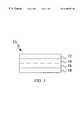
- FIG. 1is a schematic cross-section view of the DH PV converter in accordance with the present invention.
- FIG. 2is a schematic cross-section view of the structure of a discrete 0.6 eV TPV device using the DH PV converter shown in FIG. 1 .
- FIG. 3is a graph of showing the spectral quantum efficiency and reflectance for the discrete 0.6 eV TPV converter shown in FIG. 2 .
- FIG. 4is a graph showing the current-voltage for the discrete 0.6 eV TPV converter shown in FIG. 2 .
- FIG. 5is a schematic perspective view of a 0.6 eV TPV MIM structure using a variation in the DH PV converter epistructure set forth in FIG. 1 .
- FIG. 6is a preferred embodiment of the 0.6 eV TPV MIM of FIG. 5 showing incorporation of a step graded layer for growth on a binary substrate.
- FIG. 7is a graph showing the spectral AAAEQE data for a 0.6 eV MIM with, and without a back surface reflector (“BSR”).
- FIG. 8is a graph showing the current-voltage data for a 0.6 eV MIM under high-intensity illumination.
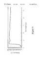
- FIG. 9is a graph showing the long-wavelength spectral reflectance data for a 0.6 eV MIM with a BSR.
- the low-bandgap, high-efficiency InAsP/GaInAs/InAsP PV DH convertersare based on the use of InAsP layers to effect passivation and minority-carrier confinement when applied to the front and back surfaces of a low-bandgap GaInAs p/n-junction absorber. This paring of the materials comprising the DH PV device provides improved performance because it reduces minority carrier recombination, resulting in a higher quantum efficiency and a lower reverse-saturation current density for the converter.
- FIG. 1the general structure of the low-bandgap high efficiency InAsP/GaInAs/InAsP PV DH converter 10 .
- the components of the DH converter 10include in optical alignment a first InP 1 ⁇ y As y n-layer 18 formed with an n-type dopant, an Ga x In 1 ⁇ x As absorber layer, the absorber layer having an n-region 16 formed with an n-type dopant and an p-region 14 formed with a p-type dopant to form a single pn-junction, and a second InP 1 ⁇ y As y p-layer 12 formed with a p-type dopant, wherein the first 18 and second 12 layers are used for passivation and minority carrier confinement of the absorber layers 14 , 16 .
- optical orientation and conductivity types of the layerscan be changed so long as the regions remain compatible and the InP 1 ⁇ y As y layers retain the passivation and confinement function in conjunction with the Ga x In 1 ⁇ x As absorber layer.
- the converter 10can be used as a discrete TPV device 20 having the below designed characteristics.
- the bandgap (E g ) of Ga x In 1 ⁇ x As as a function of x at 300° K.is given by the following mathematical equation:
- the lattice matching condition for epilayers of InAs y P 1 ⁇ y and Ga x In 1 ⁇ x Asis expressed by:
- FIG. 2a cross-sectional diagram of the discrete 0.6-eV TPV converter epistructure.
- An atmospheric pressure metalorganic vapor phase epitaxy (“APMOVPE”) growth processwhich employed a vertically oriented reactor vessel was used to yield highly uniform epilayers. This growth process has been described in U.S. Pat. No. 4,649,859 which is incorporated by reference.
- Epi-ready InP substrates 26oriented (100) 2° toward (110), were loaded directly into the reactor vessel for growth.
- Discrete converters 10were grown on polished etched S-doped InP substrates 26 and MIM structures 30 , 40 were grown on double-sided-polished (DSP) Fe-doped InP substrates 38 .
- Ethyldimethylindium, triethylgallium, arsine, and phosphinewere used as the primary reactants, and diethylzinc and hydrogen sulfide were used to dope the epilayers p- and n-type, respectively.
- Epitaxial growthwas performed in a purified hydrogen ambient at a temperature of 620° C. The deposition rates were 0.1 ⁇ m min ⁇ 1 for InAs 0.32 P 0.68 .
- the procedures used to process the devices 10 , 20 , 30 and 40are also conventional and are well known in the art.
- Selective wet-chemical etchingwas performed using 3H 3 PO 4 :4 H 2 O:1 H 2 O in order to dissolve Ga 0.32 In 0.68 As.
- Concentrated HClwas used to dissolve the InAs y P 1 ⁇ y .
- Electroplated Auwas used to form the metallizations on the discrete TPV converters 10 , 20 .
- the general methods used to fabricate the MIMscan be by any method well known in the art, but the method used in this example has been described more fully in Ward, J. S.
- Thermophotovoltaic (TPV) Power ConversionProc. 3 rd NREL Conf. on Thermophotovoltaic Generation of Electricity, AIP Conf. Proc. Vol. 401, pp. 227-236, 1997.
- the insulator used in MIM fabricationis SiO2 ( ⁇ 200 nm) and was deposited by a chemical-vapor-deposition process.
- the metallization used for the MIMswas an electron-beam-evaporated multi-metal stack consisting essentially of: Cr (30 nm); Pd (20 nm); Ag (4 um, and Pd (20 nm)).
- the optimized back-surface reflector (BSR not shown)which was applied to the back surface of the MIM converters, consisted of a MgF 2 (130 nm), Ti (2.5 nm), and Au (150 nm) formulation.
- the present examplerelates to the epitaxial growth of the 0.6-eV TPV discrete converters and MIMs.
- Discrete converters 20were fabricated using the basic DH TPV converter 10 epistructure shown in FIG. 1 .
- FIG. 2the epistructure of a preferred 0.6-eV discrete converter 20 grown lattice-mismatched on an InP substrate 26 is shown.
- the episturctureis described in optical alignment from the substrate 26 upwards.
- the basic components of the structure 20include an InAsyP 1 ⁇ y step-graded layer 24 , the 0.6-eV DH TPV converter layers 10 , and a contact layer 22 used to facilitate contacting the front surface. Details of the composition, doping level, and thickness for each of the component layers of the 0.6-eV DH TPV converter structure 20 are listed in Table 1.
- the InAsyP 1 ⁇ y graded layer 24comprises ten equal compositional steps.
- the stepsare graded in magnitude resulting in a lattice-mismatch of ⁇ 0.1% for each step interface (not shown).
- the gradingincreases from an initial compatible value on the side of the graded layer proximal to the substrate 26 surface to a final compatible value on the side of the step-graded layer which is proximal to the first n + -InP 1 ⁇ y As y layer 18 .
- the graded layer 24is terminated with the first n + -InP 1 ⁇ y As y layer 18 , which is 1 um in thickness.
- This thicker layer 18allows the final network of misfit dislocations arising from the final compositional step to evolve fully, leaving only a relatively low density of threading dislocations to propagate into the active converter layers above.
- This grading techniqueresults in converter layers 10 having excellent electronic characteristics.
- the total thickness (2.1-2.3 um) of the Ga 0.32 In 0.68 As p/n junction layers 16 and 14 , of the DH converter 10is about half the thickness normally required to provide complete absorption of the above-bandgap energy photons.
- the converter structureis designed for use as a MIM device 30 and 40 where a BSR is available to reflect unabsorbed near-bandgap-energy photons back thorough the converter layers 10 , for a second pass.
- thinner p/n-junction layers 16 and 14result in lower reverse-saturation current densities, which, in turn, result in higher converter 10 voltages ( ⁇ 18 mV higher for half the thickness, at 300 ° K.)
- thinner layers 16 and 14require less growth time, which is a potential manufacturing advantage.
- a thickness in the range of 0.1-0.3 umhas been used for the p+-Ga 0.32 In 0.68 As emitter layer 14 of the DH converter 10 .
- the microstructure of the 0.6-eV DH TPV converter 20was characterized using atomic-force microscopy (AFM), cross-sectional transmission electron microscopy (XTEM), and electron-beam-induced current (EBIC) techniques. To the naked eye, the surface of the converter 20 appears to have a fine, orthogonal, biaxial crosshatched morphology, which is typical of single-crystal lattice-mismatched III-V epilayers grown on substrates with a near ⁇ (100) orientation. Detailed examinations of the surface topography by AFM illustrated that a three-dimensional ripple morphology was superimposed on the crosshatch. The root mean-square roughness of the surface was ⁇ 23 nm.
- STEM examinationsillustrated that the structures had extensive misfit dislocation networks in the vicinity of the compositional steps in the graded region 24 .
- Threading dislocationswere observed to propagate into the DH converter 10 layers above.
- Plan-view EBICwas performed on discrete devices 10 and 20 to assess the degree of minority-carrier recombination at dislocations within the converter layers.
- the EBIC studiesshowed that carrier recombination was not occurring to any measurable degree; the threading dislocations could not be resolved as dark lines or spots.
- the above resultsindicate that the grading step 24 used for the 0.6 eV DH TPV epistructure produces converter layers having superior properties; the usual deleterious effects of threading dislocations being nonexistent.
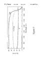
- FIG. 3the spectral quantum efficiency (QE) and reflectance (R), data for the discrete 0.6-eV DH converter 20 without an antireflection coating (“ARC”) are shown.
- the figureillustrates reflectance (R), active-area absolute external quantum efficiency (AAAEQE), and internal quantum efficiency (IQE) data for a representative high-performance 0.6 eV converter 20 .
- the IQE datashow that the carrier collection efficiency over the bulk of the response range is excellent ( ⁇ 90-100%), a result of excellent bulk material quality and low interfacial recombination at the outer edges of the p/n-junction absorber layers 14 and 16 . Again, these results corroborate the above mentioned observations made with EBIC.
- the IQErolls off, which is a result of the thin absorber layers 14 and 16 as set forth above.
- the near-band-edge QEimproves markedly when the DH converter epistructure 10 is used in a MIM 30 , 40 configuration with a BSR.
- FIG. 4the current-voltage data are shown for a representative discrete 0.6-eV converter 20 under high-intensity illumination.
- the typical photovoltaic performance parameters: open-circuit voltage (V oc ); short-circuit current density (J sc ); and fill factor (FF) are listed.
- V ocopen-circuit voltage
- J scshort-circuit current density
- FFfill factor
- Typical ranges for the diode ideality factors, and reverse-saturation current densities, for these converters 20were 0.95-1.05, and 5-10 ⁇ 10 ⁇ 7 Acm ⁇ 2 , respectively, at 25° C. These data illustrate the high-performance nature of the TPV converters 20 designed in accordance with the present invention.
- the converter epistructure 10 ( a ) for the MIM 40 fabricationis nearly identical to the epistructure 10 the 0.6-eV DH TPV discrete converters 30 , 40 , with the following exceptions: (1) the InP substrate 38 is double-sided-polished (“DSP”) and semi-insulating (“SI”)(Fe-doped and transparent to sub-bandgap-energy photons); (2) the InAs y P 1 ⁇ y compositionally graded layer 44 is undoped making it transparent to sub-bandgap-energy photons; (3) a 0.3-um-thick n+/p InAs 0.32 P 0.68 cell isolation diode (CID) 35 is included as an element of the 1-um thick n + /p InAs 0.32 P 0.68 layer 42 , 34 , 32 above the graded layer 44 ; and (4) the thickness of the p+-Ga 0/32 In 0.68 As
- the p+-Ga 0.32 In 0.68 As emitter layer 14 ( a )has a sheet resistance of ⁇ 1600 ohms per square.
- the CID 35serves two important functions. Electrical isolation of the component cells in the MIM is achieved by etching a trench (not shown) through the CID 35 n + /p junction, the reverse-bias characteristic of the CID 35 preventing inter-cell shunting, and the depth of the isolation trench (not shown) is minimized because the CID 35 is disposed directly beneath the DH converter layers 10 ( a ). This feature improves the characteristics of the cell interconnections of the MIM 40 .
- the n + -InAs 0.32 P 0.68 layer 32 of the CID 35is designed to serve the following important functions: (1) it is the back-surface confinement layer for the DH converter 10 ( a ); (2) it works as a stop-etch layer for device processing, which ensures correct placement of the back contact 22 within the MIM structure 40 ; (3) it is also the back-contact, lateral-conduction layer for the MIM 40 , the sheet resistance of the layer having 50 ohms per square, which results in negligible Joule losses; and (4) it is the emitter layer 32 for the CID 35 .
- the p-InAs 0.32 P 0.68 layer 34 of the CID 35is grown just thick enough to support the space-charge region.
- the CID elementis extremely useful in implementing MIM technology in these lattice-mismatched converter structures 30 and 40 .
- the details of the composition, doping level, and thickness for each of the component layers for the MIM 30 , 40are also listed in Table 1.
- Spectral active-area absolute external quantum efficiency (AAAEQE) data(no ARC) are shown in FIG. 7 for the MIM 40 structure with and without a BSR (not shown). The improvement in the near-bandgap response was significant. These data demonstrate that the BSR serves the intended purpose of improving the long-wavelength QE of optically thin DH converters 10 , 10 ( a ).
- High-reflectance BSRsare necessary for efficient recuperation of sub-bandgap energy photons in order to achieve high TPV system conversion efficiencies. Additionally, sub-bandgap energy free-carrier absorption within the MIM structure 40 must be as low as possible to maintain efficient recuperation.
- Long-wavelength spectral reflectance data for an as-grown, 0.6-eV MIM structure 40 (no metallization) with an optimized BSRare shown in FIG. 9 . The data show that high reflectance's (80%-90%) are achieved for wavelengths ranging from 2 to 12 um, which indicates that the BSR has a high reflectance and that the free-carrier absorption of sub-bandgap energy photons is low.
Landscapes
- Photovoltaic Devices (AREA)
Abstract
Description
| TABLE 1 |
| Preferred Material, Thickness and Dopant Densities |
| for the Various Semiconductor Layers |
| Layer | Material/Function | Thickness | Dopant density (cm-3) |
| 12 | p+-In0.32As0.68 | 30 | nm | 5 × 10¹⁸ |
| passivation/confinement/ | ||||
| window | ||||
| 14 | p+-Ga0.32In0.68As emitter | 0.1-0.3 | um | 5 × 10¹⁸ |
| 14(a) | p+-Ga0.32In0.68As emitter | 0.1 | um | 5 × 10¹⁸ |
| 16 | n−-Ga0.32In0.68As base | 2.0 | um | 3 × 10¹⁶ |
| 18 | n+-InAs0.32P0.68 | 1.0 | um | 1 × 10¹⁸ |
| passivation/confinement/ | ||||
| contact | ||||
| 22 | p+-Ga0.32In0.68As | 30 | 1 × 10¹⁹ | |
| 24 | n+-InAsyPl-ylattice step | 3.0 | um | 1 × 10¹⁸ |
| graded (y = 0.0-0.32) | ||||
| 26 | S n+-InP substrate | 350 | um | 1 × 10¹⁸ |
| 32 | n+-InAs0.32P0.68 | 0.1 | um | 7 × 10¹⁸ |
| passivation/confinement/ | ||||
| contact | ||||
| 34 | p-InAs0.32P0.68pn- | 0.2 | um | 2 × 10¹⁷ |
| junction isolation/CID | ||||
| 38 | (Fe) | 350 or 500 | um | undoped |
| semi-insulating/ | ||||
| 42 | InAs0.32P0.68buffer | 0.7 | um | undoped |
| 44 | InAsyPl-ylattice step | 3.0 | um | undoped |
| graded (y = 0.0-0.32) | ||||
Claims (17)
Priority Applications (1)
| Application Number | Priority Date | Filing Date | Title |
|---|---|---|---|
| US09/416,014US6300557B1 (en) | 1998-10-09 | 1999-10-08 | Low-bandgap double-heterostructure InAsP/GaInAs photovoltaic converters |
Applications Claiming Priority (2)
| Application Number | Priority Date | Filing Date | Title |
|---|---|---|---|
| US10376898P | 1998-10-09 | 1998-10-09 | |
| US09/416,014US6300557B1 (en) | 1998-10-09 | 1999-10-08 | Low-bandgap double-heterostructure InAsP/GaInAs photovoltaic converters |
Publications (1)
| Publication Number | Publication Date |
|---|---|
| US6300557B1true US6300557B1 (en) | 2001-10-09 |
Family
ID=26800832
Family Applications (1)
| Application Number | Title | Priority Date | Filing Date |
|---|---|---|---|
| US09/416,014Expired - LifetimeUS6300557B1 (en) | 1998-10-09 | 1999-10-08 | Low-bandgap double-heterostructure InAsP/GaInAs photovoltaic converters |
Country Status (1)
| Country | Link |
|---|---|
| US (1) | US6300557B1 (en) |
Cited By (100)
| Publication number | Priority date | Publication date | Assignee | Title |
|---|---|---|---|---|
| US6482672B1 (en)* | 1997-11-06 | 2002-11-19 | Essential Research, Inc. | Using a critical composition grading technique to deposit InGaAs epitaxial layers on InP substrates |
| US20030034065A1 (en)* | 2001-08-14 | 2003-02-20 | The Charles Stark Draper Laboratory, Inc. | Method and device for selectively emitting photons |
| US6563264B2 (en)* | 2000-07-25 | 2003-05-13 | Hamamatsu Photonics K.K. | Photocathode and electron tube |
| US20030136442A1 (en)* | 2002-01-23 | 2003-07-24 | Tatsuya Takamoto | Group III-V solar cell |
| US6603184B2 (en)* | 2000-09-06 | 2003-08-05 | Applied Optoelectronics, Inc. | Double heterostructure photodiode with graded minority-carrier blocking structures |
| WO2003100868A1 (en)* | 2002-05-21 | 2003-12-04 | Midwest Research Institute | Low-bandgap, monolithic, multi-bandgap, optoelectronic devices |
| US6660928B1 (en) | 2002-04-02 | 2003-12-09 | Essential Research, Inc. | Multi-junction photovoltaic cell |
| US6727530B1 (en) | 2003-03-04 | 2004-04-27 | Xindium Technologies, Inc. | Integrated photodetector and heterojunction bipolar transistors |
| US20060144435A1 (en)* | 2002-05-21 | 2006-07-06 | Wanlass Mark W | High-efficiency, monolithic, multi-bandgap, tandem photovoltaic energy converters |
| US20060162768A1 (en)* | 2002-05-21 | 2006-07-27 | Wanlass Mark W | Low bandgap, monolithic, multi-bandgap, optoelectronic devices |
| WO2008080160A1 (en)* | 2006-12-22 | 2008-07-03 | Advent Solar, Inc. | Interconnect technologies for back contact solar cells and modules |
| US20080185038A1 (en)* | 2007-02-02 | 2008-08-07 | Emcore Corporation | Inverted metamorphic solar cell with via for backside contacts |
| US20080245409A1 (en)* | 2006-12-27 | 2008-10-09 | Emcore Corporation | Inverted Metamorphic Solar Cell Mounted on Flexible Film |
| US20090032086A1 (en)* | 2007-07-30 | 2009-02-05 | Emcore Corporation | Terrestrial solar array including a rigid support frame |
| US20090032090A1 (en)* | 2007-07-30 | 2009-02-05 | Emcore Corporation | Method for assembling a terrestrial solar array including a rigid support frame |
| US20090038679A1 (en)* | 2007-08-09 | 2009-02-12 | Emcore Corporation | Thin Multijunction Solar Cells With Plated Metal OHMIC Contact and Support |
| US20090078308A1 (en)* | 2007-09-24 | 2009-03-26 | Emcore Corporation | Thin Inverted Metamorphic Multijunction Solar Cells with Rigid Support |
| US20090078310A1 (en)* | 2007-09-24 | 2009-03-26 | Emcore Corporation | Heterojunction Subcells In Inverted Metamorphic Multijunction Solar Cells |
| US20090078311A1 (en)* | 2007-09-24 | 2009-03-26 | Emcore Corporation | Surfactant Assisted Growth in Barrier Layers In Inverted Metamorphic Multijunction Solar Cells |
| US20090078309A1 (en)* | 2007-09-24 | 2009-03-26 | Emcore Corporation | Barrier Layers In Inverted Metamorphic Multijunction Solar Cells |
| US20090155952A1 (en)* | 2007-12-13 | 2009-06-18 | Emcore Corporation | Exponentially Doped Layers In Inverted Metamorphic Multijunction Solar Cells |
| JP2009141135A (en)* | 2007-12-06 | 2009-06-25 | Sharp Corp | Multilayer compound semiconductor solar cell |
| US20090223554A1 (en)* | 2008-03-05 | 2009-09-10 | Emcore Corporation | Dual Sided Photovoltaic Package |
| US20090229662A1 (en)* | 2008-03-13 | 2009-09-17 | Emcore Corporation | Off-Cut Substrates In Inverted Metamorphic Multijunction Solar Cells |
| US20090229659A1 (en)* | 2002-05-21 | 2009-09-17 | Midwest Research Institute | Monolithic, multi-bandgap, tandem, ultra-thin, strain-counterbalanced, photovoltaic energy converters with optimal subcell bandgaps |
| US20090272438A1 (en)* | 2008-05-05 | 2009-11-05 | Emcore Corporation | Strain Balanced Multiple Quantum Well Subcell In Inverted Metamorphic Multijunction Solar Cell |
| US20090272430A1 (en)* | 2008-04-30 | 2009-11-05 | Emcore Solar Power, Inc. | Refractive Index Matching in Inverted Metamorphic Multijunction Solar Cells |
| US20090288703A1 (en)* | 2008-05-20 | 2009-11-26 | Emcore Corporation | Wide Band Gap Window Layers In Inverted Metamorphic Multijunction Solar Cells |
| US20090314348A1 (en)* | 2006-08-07 | 2009-12-24 | Mcglynn Daniel | Terrestrial solar power system using iii-v semiconductor solar cells |
| US20090320922A1 (en)* | 2004-02-05 | 2009-12-31 | Advent Solar, Inc. | Contact Fabrication of Emitter Wrap-Through Back Contact Silicon Solar Cells |
| US20100012175A1 (en)* | 2008-07-16 | 2010-01-21 | Emcore Solar Power, Inc. | Ohmic n-contact formed at low temperature in inverted metamorphic multijunction solar cells |
| US20100012174A1 (en)* | 2008-07-16 | 2010-01-21 | Emcore Corporation | High band gap contact layer in inverted metamorphic multijunction solar cells |
| US20100031994A1 (en)* | 2008-08-07 | 2010-02-11 | Emcore Corporation | Wafer Level Interconnection of Inverted Metamorphic Multijunction Solar Cells |
| US20100041178A1 (en)* | 2008-08-12 | 2010-02-18 | Emcore Solar Power, Inc. | Demounting of Inverted Metamorphic Multijunction Solar Cells |
| US20100047959A1 (en)* | 2006-08-07 | 2010-02-25 | Emcore Solar Power, Inc. | Epitaxial Lift Off on Film Mounted Inverted Metamorphic Multijunction Solar Cells |
| US20100096001A1 (en)* | 2008-10-22 | 2010-04-22 | Epir Technologies, Inc. | High efficiency multijunction ii-vi photovoltaic solar cells |
| US20100108860A1 (en)* | 2008-10-24 | 2010-05-06 | Emcore Solar Power, Inc. | Techniques for Monitoring Solar Array Performance and Applications Thereof |
| US20100116327A1 (en)* | 2008-11-10 | 2010-05-13 | Emcore Corporation | Four junction inverted metamorphic multijunction solar cell |
| US20100122764A1 (en)* | 2008-11-14 | 2010-05-20 | Emcore Solar Power, Inc. | Surrogate Substrates for Inverted Metamorphic Multijunction Solar Cells |
| US20100147366A1 (en)* | 2008-12-17 | 2010-06-17 | Emcore Solar Power, Inc. | Inverted Metamorphic Multijunction Solar Cells with Distributed Bragg Reflector |
| US20100186804A1 (en)* | 2009-01-29 | 2010-07-29 | Emcore Solar Power, Inc. | String Interconnection of Inverted Metamorphic Multijunction Solar Cells on Flexible Perforated Carriers |
| US20100203730A1 (en)* | 2009-02-09 | 2010-08-12 | Emcore Solar Power, Inc. | Epitaxial Lift Off in Inverted Metamorphic Multijunction Solar Cells |
| US20100206365A1 (en)* | 2009-02-19 | 2010-08-19 | Emcore Solar Power, Inc. | Inverted Metamorphic Multijunction Solar Cells on Low Density Carriers |
| US7785989B2 (en) | 2008-12-17 | 2010-08-31 | Emcore Solar Power, Inc. | Growth substrates for inverted metamorphic multijunction solar cells |
| US20100229926A1 (en)* | 2009-03-10 | 2010-09-16 | Emcore Solar Power, Inc. | Four Junction Inverted Metamorphic Multijunction Solar Cell with a Single Metamorphic Layer |
| US20100233838A1 (en)* | 2009-03-10 | 2010-09-16 | Emcore Solar Power, Inc. | Mounting of Solar Cells on a Flexible Substrate |
| US20100229933A1 (en)* | 2009-03-10 | 2010-09-16 | Emcore Solar Power, Inc. | Inverted Metamorphic Multijunction Solar Cells with a Supporting Coating |
| US20100229913A1 (en)* | 2009-01-29 | 2010-09-16 | Emcore Solar Power, Inc. | Contact Layout and String Interconnection of Inverted Metamorphic Multijunction Solar Cells |
| US20100233839A1 (en)* | 2009-01-29 | 2010-09-16 | Emcore Solar Power, Inc. | String Interconnection and Fabrication of Inverted Metamorphic Multijunction Solar Cells |
| US20100282288A1 (en)* | 2009-05-06 | 2010-11-11 | Emcore Solar Power, Inc. | Solar Cell Interconnection on a Flexible Substrate |
| US20110030774A1 (en)* | 2009-08-07 | 2011-02-10 | Emcore Solar Power, Inc. | Inverted Metamorphic Multijunction Solar Cells with Back Contacts |
| US20110041898A1 (en)* | 2009-08-19 | 2011-02-24 | Emcore Solar Power, Inc. | Back Metal Layers in Inverted Metamorphic Multijunction Solar Cells |
| WO2011035265A1 (en)* | 2009-09-18 | 2011-03-24 | Soraa, Inc. | Power light emitting diode and method with current density operation |
| US20110073887A1 (en)* | 2009-09-25 | 2011-03-31 | Alliance For Sustainable Energy, Llc | Optoelectronic devices having a direct-band-gap base and an indirect-band-gap emitter |
| US7939428B2 (en) | 2000-11-27 | 2011-05-10 | S.O.I.Tec Silicon On Insulator Technologies | Methods for making substrates and substrates formed therefrom |
| CN102117849A (en)* | 2009-12-31 | 2011-07-06 | 晶元光电股份有限公司 | Solar cell element and its device |
| US20110186115A1 (en)* | 2004-12-30 | 2011-08-04 | Alliance For Sustainable Energy, Llc | High Performance, High Bandgap, Lattice-Mismatched, GaInP Solar Cells |
| US8187907B1 (en) | 2010-05-07 | 2012-05-29 | Emcore Solar Power, Inc. | Solder structures for fabrication of inverted metamorphic multijunction solar cells |
| US20120305059A1 (en)* | 2011-06-06 | 2012-12-06 | Alta Devices, Inc. | Photon recycling in an optoelectronic device |
| WO2012021227A3 (en)* | 2010-08-09 | 2012-12-27 | The Boeing Company | Heterojunction solar cell |
| US8513514B2 (en) | 2008-10-24 | 2013-08-20 | Suncore Photovoltaics, Inc. | Solar tracking for terrestrial solar arrays with variable start and stop positions |
| US8536445B2 (en) | 2006-06-02 | 2013-09-17 | Emcore Solar Power, Inc. | Inverted metamorphic multijunction solar cells |
| US8686282B2 (en) | 2006-08-07 | 2014-04-01 | Emcore Solar Power, Inc. | Solar power system for space vehicles or satellites using inverted metamorphic multijunction solar cells |
| US8759138B2 (en) | 2008-02-11 | 2014-06-24 | Suncore Photovoltaics, Inc. | Concentrated photovoltaic system modules using III-V semiconductor solar cells |
| US8778199B2 (en) | 2009-02-09 | 2014-07-15 | Emoore Solar Power, Inc. | Epitaxial lift off in inverted metamorphic multijunction solar cells |
| US20140238474A1 (en)* | 2013-02-25 | 2014-08-28 | United States Department Of Energy | Mercapto-based coupling agent for improved thermophotovoltaic device back surface reflector adhesion and relfectance |
| US8895342B2 (en) | 2007-09-24 | 2014-11-25 | Emcore Solar Power, Inc. | Heterojunction subcells in inverted metamorphic multijunction solar cells |
| US9012771B1 (en) | 2009-09-03 | 2015-04-21 | Suncore Photovoltaics, Inc. | Solar cell receiver subassembly with a heat shield for use in a concentrating solar system |
| US9018521B1 (en) | 2008-12-17 | 2015-04-28 | Solaero Technologies Corp. | Inverted metamorphic multijunction solar cell with DBR layer adjacent to the top subcell |
| US9018519B1 (en) | 2009-03-10 | 2015-04-28 | Solaero Technologies Corp. | Inverted metamorphic multijunction solar cells having a permanent supporting substrate |
| US9117966B2 (en) | 2007-09-24 | 2015-08-25 | Solaero Technologies Corp. | Inverted metamorphic multijunction solar cell with two metamorphic layers and homojunction top cell |
| US9190555B2 (en) | 2008-07-17 | 2015-11-17 | Uriel Solar, Inc. | Polycrystalline CdTe thin film semiconductor photovoltaic cell structures for use in solar electricity generation |
| US9287438B1 (en)* | 2008-07-16 | 2016-03-15 | Solaero Technologies Corp. | Method for forming ohmic N-contacts at low temperature in inverted metamorphic multijunction solar cells with contaminant isolation |
| US9293644B2 (en) | 2009-09-18 | 2016-03-22 | Soraa, Inc. | Power light emitting diode and method with uniform current density operation |
| US9331228B2 (en) | 2008-02-11 | 2016-05-03 | Suncore Photovoltaics, Inc. | Concentrated photovoltaic system modules using III-V semiconductor solar cells |
| US9410664B2 (en) | 2013-08-29 | 2016-08-09 | Soraa, Inc. | Circadian friendly LED light source |
| US9543468B2 (en) | 2010-10-12 | 2017-01-10 | Alliance For Sustainable Energy, Llc | High bandgap III-V alloys for high efficiency optoelectronics |
| US9583678B2 (en) | 2009-09-18 | 2017-02-28 | Soraa, Inc. | High-performance LED fabrication |
| US9590131B2 (en) | 2013-03-27 | 2017-03-07 | Alliance For Sustainable Energy, Llc | Systems and methods for advanced ultra-high-performance InP solar cells |
| US9634172B1 (en) | 2007-09-24 | 2017-04-25 | Solaero Technologies Corp. | Inverted metamorphic multijunction solar cell with multiple metamorphic layers |
| US9691929B2 (en) | 2008-11-14 | 2017-06-27 | Solaero Technologies Corp. | Four junction inverted metamorphic multijunction solar cell with two metamorphic layers |
| US9761763B2 (en) | 2012-12-21 | 2017-09-12 | Soraa, Inc. | Dense-luminescent-materials-coated violet LEDs |
| US9806215B2 (en) | 2009-09-03 | 2017-10-31 | Suncore Photovoltaics, Inc. | Encapsulated concentrated photovoltaic system subassembly for III-V semiconductor solar cells |
| US9935209B2 (en) | 2016-01-28 | 2018-04-03 | Solaero Technologies Corp. | Multijunction metamorphic solar cell for space applications |
| US9985161B2 (en) | 2016-08-26 | 2018-05-29 | Solaero Technologies Corp. | Multijunction metamorphic solar cell for space applications |
| US10153388B1 (en) | 2013-03-15 | 2018-12-11 | Solaero Technologies Corp. | Emissivity coating for space solar cell arrays |
| US10170656B2 (en) | 2009-03-10 | 2019-01-01 | Solaero Technologies Corp. | Inverted metamorphic multijunction solar cell with a single metamorphic layer |
| US10256359B2 (en) | 2015-10-19 | 2019-04-09 | Solaero Technologies Corp. | Lattice matched multijunction solar cell assemblies for space applications |
| US10263134B1 (en) | 2016-05-25 | 2019-04-16 | Solaero Technologies Corp. | Multijunction solar cells having an indirect high band gap semiconductor emitter layer in the upper solar subcell |
| US10270000B2 (en) | 2015-10-19 | 2019-04-23 | Solaero Technologies Corp. | Multijunction metamorphic solar cell assembly for space applications |
| US10361330B2 (en) | 2015-10-19 | 2019-07-23 | Solaero Technologies Corp. | Multijunction solar cell assemblies for space applications |
| US10381505B2 (en) | 2007-09-24 | 2019-08-13 | Solaero Technologies Corp. | Inverted metamorphic multijunction solar cells including metamorphic layers |
| US10381501B2 (en) | 2006-06-02 | 2019-08-13 | Solaero Technologies Corp. | Inverted metamorphic multijunction solar cell with multiple metamorphic layers |
| US10403778B2 (en) | 2015-10-19 | 2019-09-03 | Solaero Technologies Corp. | Multijunction solar cell assembly for space applications |
| US10541349B1 (en) | 2008-12-17 | 2020-01-21 | Solaero Technologies Corp. | Methods of forming inverted multijunction solar cells with distributed Bragg reflector |
| US10557595B2 (en) | 2009-09-18 | 2020-02-11 | Soraa, Inc. | LED lamps with improved quality of light |
| US10636926B1 (en) | 2016-12-12 | 2020-04-28 | Solaero Technologies Corp. | Distributed BRAGG reflector structures in multijunction solar cells |
| US11569404B2 (en) | 2017-12-11 | 2023-01-31 | Solaero Technologies Corp. | Multijunction solar cells |
| RU2806342C1 (en)* | 2023-03-13 | 2023-10-31 | Федеральное государственное бюджетное учреждение науки Физико-технический институт им. А.Ф. Иоффе Российской академии наук | Laser radiation photo detector |
| US12249667B2 (en) | 2017-08-18 | 2025-03-11 | Solaero Technologies Corp. | Space vehicles including multijunction metamorphic solar cells |
Citations (18)
| Publication number | Priority date | Publication date | Assignee | Title |
|---|---|---|---|---|
| US4017332A (en)* | 1975-02-27 | 1977-04-12 | Varian Associates | Solar cells employing stacked opposite conductivity layers |
| US4291323A (en)* | 1980-05-01 | 1981-09-22 | Bell Telephone Laboratories, Incorporated | Indium phosphide arsenide based devices |
| US4633030A (en) | 1985-08-05 | 1986-12-30 | Holobeam, Inc. | Photovoltaic cells on lattice-mismatched crystal substrates |
| US4846896A (en) | 1987-07-08 | 1989-07-11 | Mitsubishi Denki Kabushiki Kaisha | Solar cell with integral reverse voltage protection diode |
| US5266125A (en) | 1992-05-12 | 1993-11-30 | Astropower, Inc. | Interconnected silicon film solar cell array |
| US5322572A (en)* | 1989-11-03 | 1994-06-21 | The United States Of America As Represented By The United States Department Of Energy | Monolithic tandem solar cell |
| US5389158A (en) | 1989-04-17 | 1995-02-14 | The Boeing Company | Low bandgap photovoltaic cell with inherent bypass diode |
| US5471076A (en)* | 1993-01-14 | 1995-11-28 | Hamamatsu Photonics K.K. | Semiconductor light-receiving device with graded layer |
| US5479032A (en)* | 1994-07-21 | 1995-12-26 | Trustees Of Princeton University | Multiwavelength infrared focal plane array detector |
| US5593901A (en) | 1989-09-08 | 1997-01-14 | Amoco/Enron Solar | Monolithic series and parallel connected photovoltaic module |
| US5616185A (en) | 1995-10-10 | 1997-04-01 | Hughes Aircraft Company | Solar cell with integrated bypass diode and method |
| US5769964A (en) | 1996-08-29 | 1998-06-23 | The United States Of America As Reprresented By The United States Department Of Energy | Bulk single crystal ternary substrates for a thermophotovoltaic energy conversion system |
| US5800630A (en)* | 1993-04-08 | 1998-09-01 | University Of Houston | Tandem solar cell with indium phosphide tunnel junction |
| US5851310A (en)* | 1995-12-06 | 1998-12-22 | University Of Houston | Strained quantum well photovoltaic energy converter |
| US5853497A (en) | 1996-12-12 | 1998-12-29 | Hughes Electronics Corporation | High efficiency multi-junction solar cells |
| US6043426A (en)* | 1998-02-20 | 2000-03-28 | The United States Of America As Represented By The United States Department Of Energy | Thermophotovoltaic energy conversion system having a heavily doped n-type region |
| US6057506A (en)* | 1998-03-23 | 2000-05-02 | The United States Of America As Represented By The United States Department Of Energy | Variable current-voltage TPV device for use in a thermophotovoltaic energy conversion system |
| US6162987A (en)* | 1999-06-30 | 2000-12-19 | The United States Of America As Represented By The United States Department Of Energy | Monolithic interconnected module with a tunnel junction for enhanced electrical and optical performance |
- 1999
- 1999-10-08USUS09/416,014patent/US6300557B1/ennot_activeExpired - Lifetime
Patent Citations (18)
| Publication number | Priority date | Publication date | Assignee | Title |
|---|---|---|---|---|
| US4017332A (en)* | 1975-02-27 | 1977-04-12 | Varian Associates | Solar cells employing stacked opposite conductivity layers |
| US4291323A (en)* | 1980-05-01 | 1981-09-22 | Bell Telephone Laboratories, Incorporated | Indium phosphide arsenide based devices |
| US4633030A (en) | 1985-08-05 | 1986-12-30 | Holobeam, Inc. | Photovoltaic cells on lattice-mismatched crystal substrates |
| US4846896A (en) | 1987-07-08 | 1989-07-11 | Mitsubishi Denki Kabushiki Kaisha | Solar cell with integral reverse voltage protection diode |
| US5389158A (en) | 1989-04-17 | 1995-02-14 | The Boeing Company | Low bandgap photovoltaic cell with inherent bypass diode |
| US5593901A (en) | 1989-09-08 | 1997-01-14 | Amoco/Enron Solar | Monolithic series and parallel connected photovoltaic module |
| US5322572A (en)* | 1989-11-03 | 1994-06-21 | The United States Of America As Represented By The United States Department Of Energy | Monolithic tandem solar cell |
| US5266125A (en) | 1992-05-12 | 1993-11-30 | Astropower, Inc. | Interconnected silicon film solar cell array |
| US5471076A (en)* | 1993-01-14 | 1995-11-28 | Hamamatsu Photonics K.K. | Semiconductor light-receiving device with graded layer |
| US5800630A (en)* | 1993-04-08 | 1998-09-01 | University Of Houston | Tandem solar cell with indium phosphide tunnel junction |
| US5479032A (en)* | 1994-07-21 | 1995-12-26 | Trustees Of Princeton University | Multiwavelength infrared focal plane array detector |
| US5616185A (en) | 1995-10-10 | 1997-04-01 | Hughes Aircraft Company | Solar cell with integrated bypass diode and method |
| US5851310A (en)* | 1995-12-06 | 1998-12-22 | University Of Houston | Strained quantum well photovoltaic energy converter |
| US5769964A (en) | 1996-08-29 | 1998-06-23 | The United States Of America As Reprresented By The United States Department Of Energy | Bulk single crystal ternary substrates for a thermophotovoltaic energy conversion system |
| US5853497A (en) | 1996-12-12 | 1998-12-29 | Hughes Electronics Corporation | High efficiency multi-junction solar cells |
| US6043426A (en)* | 1998-02-20 | 2000-03-28 | The United States Of America As Represented By The United States Department Of Energy | Thermophotovoltaic energy conversion system having a heavily doped n-type region |
| US6057506A (en)* | 1998-03-23 | 2000-05-02 | The United States Of America As Represented By The United States Department Of Energy | Variable current-voltage TPV device for use in a thermophotovoltaic energy conversion system |
| US6162987A (en)* | 1999-06-30 | 2000-12-19 | The United States Of America As Represented By The United States Department Of Energy | Monolithic interconnected module with a tunnel junction for enhanced electrical and optical performance |
Non-Patent Citations (2)
| Title |
|---|
| Electronics Letters, 24(7), pp. 379-380, Mar. 1988.* |
| Webb et al, Vibrational Spectroscopy, vol. 21, pp. 3-15, Dec. 1999.* |
Cited By (149)
| Publication number | Priority date | Publication date | Assignee | Title |
|---|---|---|---|---|
| US6482672B1 (en)* | 1997-11-06 | 2002-11-19 | Essential Research, Inc. | Using a critical composition grading technique to deposit InGaAs epitaxial layers on InP substrates |
| US6563264B2 (en)* | 2000-07-25 | 2003-05-13 | Hamamatsu Photonics K.K. | Photocathode and electron tube |
| US6603184B2 (en)* | 2000-09-06 | 2003-08-05 | Applied Optoelectronics, Inc. | Double heterostructure photodiode with graded minority-carrier blocking structures |
| US7939428B2 (en) | 2000-11-27 | 2011-05-10 | S.O.I.Tec Silicon On Insulator Technologies | Methods for making substrates and substrates formed therefrom |
| US20030034065A1 (en)* | 2001-08-14 | 2003-02-20 | The Charles Stark Draper Laboratory, Inc. | Method and device for selectively emitting photons |
| US20030136442A1 (en)* | 2002-01-23 | 2003-07-24 | Tatsuya Takamoto | Group III-V solar cell |
| US6660928B1 (en) | 2002-04-02 | 2003-12-09 | Essential Research, Inc. | Multi-junction photovoltaic cell |
| US20060162768A1 (en)* | 2002-05-21 | 2006-07-27 | Wanlass Mark W | Low bandgap, monolithic, multi-bandgap, optoelectronic devices |
| US8772623B2 (en) | 2002-05-21 | 2014-07-08 | Alliance For Sustainable Energy, Llc | Low-bandgap, monolithic, multi-bandgap, optoelectronic devices |
| US20060144435A1 (en)* | 2002-05-21 | 2006-07-06 | Wanlass Mark W | High-efficiency, monolithic, multi-bandgap, tandem photovoltaic energy converters |
| US9293615B2 (en) | 2002-05-21 | 2016-03-22 | Alliance For Sustainable Energy, Llc | Low-bandgap, monolithic, multi-bandgap, optoelectronic devices |
| US8067687B2 (en) | 2002-05-21 | 2011-11-29 | Alliance For Sustainable Energy, Llc | High-efficiency, monolithic, multi-bandgap, tandem photovoltaic energy converters |
| US8173891B2 (en) | 2002-05-21 | 2012-05-08 | Alliance For Sustainable Energy, Llc | Monolithic, multi-bandgap, tandem, ultra-thin, strain-counterbalanced, photovoltaic energy converters with optimal subcell bandgaps |
| WO2003100868A1 (en)* | 2002-05-21 | 2003-12-04 | Midwest Research Institute | Low-bandgap, monolithic, multi-bandgap, optoelectronic devices |
| US9231135B2 (en) | 2002-05-21 | 2016-01-05 | Alliance For Sustainable Energy, Llc | Low-bandgap, monolithic, multi-bandgap, optoelectronic devices |
| US8735202B2 (en) | 2002-05-21 | 2014-05-27 | Alliance For Sustainable Energy, Llc | High-efficiency, monolithic, multi-bandgap, tandem, photovoltaic energy converters |
| US20090229659A1 (en)* | 2002-05-21 | 2009-09-17 | Midwest Research Institute | Monolithic, multi-bandgap, tandem, ultra-thin, strain-counterbalanced, photovoltaic energy converters with optimal subcell bandgaps |
| US20040173817A1 (en)* | 2003-03-04 | 2004-09-09 | Milton Feng | Integrated photodetector and heterojunction bipolar transistors |
| US6727530B1 (en) | 2003-03-04 | 2004-04-27 | Xindium Technologies, Inc. | Integrated photodetector and heterojunction bipolar transistors |
| US7863084B2 (en) | 2004-02-05 | 2011-01-04 | Applied Materials, Inc | Contact fabrication of emitter wrap-through back contact silicon solar cells |
| US20090320922A1 (en)* | 2004-02-05 | 2009-12-31 | Advent Solar, Inc. | Contact Fabrication of Emitter Wrap-Through Back Contact Silicon Solar Cells |
| US9484480B2 (en) | 2004-12-30 | 2016-11-01 | Alliance For Sustainable Energy, Llc | High performance, high bandgap, lattice-mismatched, GaInP solar cells |
| US20110186115A1 (en)* | 2004-12-30 | 2011-08-04 | Alliance For Sustainable Energy, Llc | High Performance, High Bandgap, Lattice-Mismatched, GaInP Solar Cells |
| US8772628B2 (en) | 2004-12-30 | 2014-07-08 | Alliance For Sustainable Energy, Llc | High performance, high bandgap, lattice-mismatched, GaInP solar cells |
| US10026860B2 (en) | 2006-06-02 | 2018-07-17 | Solaero Technologies Corp. | Metamorphic layers in multijunction solar cells |
| US10381501B2 (en) | 2006-06-02 | 2019-08-13 | Solaero Technologies Corp. | Inverted metamorphic multijunction solar cell with multiple metamorphic layers |
| US10553740B2 (en) | 2006-06-02 | 2020-02-04 | Solaero Technologies Corp. | Metamorphic layers in multijunction solar cells |
| US8536445B2 (en) | 2006-06-02 | 2013-09-17 | Emcore Solar Power, Inc. | Inverted metamorphic multijunction solar cells |
| US20090314348A1 (en)* | 2006-08-07 | 2009-12-24 | Mcglynn Daniel | Terrestrial solar power system using iii-v semiconductor solar cells |
| US8686282B2 (en) | 2006-08-07 | 2014-04-01 | Emcore Solar Power, Inc. | Solar power system for space vehicles or satellites using inverted metamorphic multijunction solar cells |
| US8513518B2 (en) | 2006-08-07 | 2013-08-20 | Emcore Solar Power, Inc. | Terrestrial solar power system using III-V semiconductor solar cells |
| US20100047959A1 (en)* | 2006-08-07 | 2010-02-25 | Emcore Solar Power, Inc. | Epitaxial Lift Off on Film Mounted Inverted Metamorphic Multijunction Solar Cells |
| WO2008080160A1 (en)* | 2006-12-22 | 2008-07-03 | Advent Solar, Inc. | Interconnect technologies for back contact solar cells and modules |
| US20080245409A1 (en)* | 2006-12-27 | 2008-10-09 | Emcore Corporation | Inverted Metamorphic Solar Cell Mounted on Flexible Film |
| US20080185038A1 (en)* | 2007-02-02 | 2008-08-07 | Emcore Corporation | Inverted metamorphic solar cell with via for backside contacts |
| US20090032090A1 (en)* | 2007-07-30 | 2009-02-05 | Emcore Corporation | Method for assembling a terrestrial solar array including a rigid support frame |
| US20090032086A1 (en)* | 2007-07-30 | 2009-02-05 | Emcore Corporation | Terrestrial solar array including a rigid support frame |
| US20090038679A1 (en)* | 2007-08-09 | 2009-02-12 | Emcore Corporation | Thin Multijunction Solar Cells With Plated Metal OHMIC Contact and Support |
| US9634172B1 (en) | 2007-09-24 | 2017-04-25 | Solaero Technologies Corp. | Inverted metamorphic multijunction solar cell with multiple metamorphic layers |
| US8895342B2 (en) | 2007-09-24 | 2014-11-25 | Emcore Solar Power, Inc. | Heterojunction subcells in inverted metamorphic multijunction solar cells |
| US10374112B2 (en) | 2007-09-24 | 2019-08-06 | Solaero Technologies Corp. | Inverted metamorphic multijunction solar cell including a metamorphic layer |
| US10381505B2 (en) | 2007-09-24 | 2019-08-13 | Solaero Technologies Corp. | Inverted metamorphic multijunction solar cells including metamorphic layers |
| US20090078308A1 (en)* | 2007-09-24 | 2009-03-26 | Emcore Corporation | Thin Inverted Metamorphic Multijunction Solar Cells with Rigid Support |
| US9356176B2 (en) | 2007-09-24 | 2016-05-31 | Solaero Technologies Corp. | Inverted metamorphic multijunction solar cell with metamorphic layers |
| US20090078310A1 (en)* | 2007-09-24 | 2009-03-26 | Emcore Corporation | Heterojunction Subcells In Inverted Metamorphic Multijunction Solar Cells |
| US20090078309A1 (en)* | 2007-09-24 | 2009-03-26 | Emcore Corporation | Barrier Layers In Inverted Metamorphic Multijunction Solar Cells |
| US20090078311A1 (en)* | 2007-09-24 | 2009-03-26 | Emcore Corporation | Surfactant Assisted Growth in Barrier Layers In Inverted Metamorphic Multijunction Solar Cells |
| US9231147B2 (en) | 2007-09-24 | 2016-01-05 | Solaero Technologies Corp. | Heterojunction subcells in inverted metamorphic multijunction solar cells |
| US9117966B2 (en) | 2007-09-24 | 2015-08-25 | Solaero Technologies Corp. | Inverted metamorphic multijunction solar cell with two metamorphic layers and homojunction top cell |
| JP2009141135A (en)* | 2007-12-06 | 2009-06-25 | Sharp Corp | Multilayer compound semiconductor solar cell |
| US20090155952A1 (en)* | 2007-12-13 | 2009-06-18 | Emcore Corporation | Exponentially Doped Layers In Inverted Metamorphic Multijunction Solar Cells |
| US7727795B2 (en) | 2007-12-13 | 2010-06-01 | Encore Solar Power, Inc. | Exponentially doped layers in inverted metamorphic multijunction solar cells |
| US20090155951A1 (en)* | 2007-12-13 | 2009-06-18 | Emcore Corporation | Exponentially Doped Layers In Inverted Metamorphic Multijunction Solar Cells |
| US8946608B2 (en) | 2008-02-01 | 2015-02-03 | Suncore Photovoltaics, Inc. | Solar tracking system |
| US9331228B2 (en) | 2008-02-11 | 2016-05-03 | Suncore Photovoltaics, Inc. | Concentrated photovoltaic system modules using III-V semiconductor solar cells |
| US8759138B2 (en) | 2008-02-11 | 2014-06-24 | Suncore Photovoltaics, Inc. | Concentrated photovoltaic system modules using III-V semiconductor solar cells |
| US9923112B2 (en) | 2008-02-11 | 2018-03-20 | Suncore Photovoltaics, Inc. | Concentrated photovoltaic system modules using III-V semiconductor solar cells |
| US20090223554A1 (en)* | 2008-03-05 | 2009-09-10 | Emcore Corporation | Dual Sided Photovoltaic Package |
| US20090229662A1 (en)* | 2008-03-13 | 2009-09-17 | Emcore Corporation | Off-Cut Substrates In Inverted Metamorphic Multijunction Solar Cells |
| US20090272430A1 (en)* | 2008-04-30 | 2009-11-05 | Emcore Solar Power, Inc. | Refractive Index Matching in Inverted Metamorphic Multijunction Solar Cells |
| US20090272438A1 (en)* | 2008-05-05 | 2009-11-05 | Emcore Corporation | Strain Balanced Multiple Quantum Well Subcell In Inverted Metamorphic Multijunction Solar Cell |
| US20090288703A1 (en)* | 2008-05-20 | 2009-11-26 | Emcore Corporation | Wide Band Gap Window Layers In Inverted Metamorphic Multijunction Solar Cells |
| US9601652B2 (en) | 2008-07-16 | 2017-03-21 | Solaero Technologies Corp. | Ohmic N-contact formed at low temperature in inverted metamorphic multijunction solar cells |
| US9287438B1 (en)* | 2008-07-16 | 2016-03-15 | Solaero Technologies Corp. | Method for forming ohmic N-contacts at low temperature in inverted metamorphic multijunction solar cells with contaminant isolation |
| US8753918B2 (en) | 2008-07-16 | 2014-06-17 | Emcore Solar Power, Inc. | Gallium arsenide solar cell with germanium/palladium contact |
| US20100012175A1 (en)* | 2008-07-16 | 2010-01-21 | Emcore Solar Power, Inc. | Ohmic n-contact formed at low temperature in inverted metamorphic multijunction solar cells |
| US20100012174A1 (en)* | 2008-07-16 | 2010-01-21 | Emcore Corporation | High band gap contact layer in inverted metamorphic multijunction solar cells |
| US8987042B2 (en) | 2008-07-16 | 2015-03-24 | Solaero Technologies Corp. | Ohmic N-contact formed at low temperature in inverted metamorphic multijunction solar cells |
| US9190555B2 (en) | 2008-07-17 | 2015-11-17 | Uriel Solar, Inc. | Polycrystalline CdTe thin film semiconductor photovoltaic cell structures for use in solar electricity generation |
| US8263853B2 (en) | 2008-08-07 | 2012-09-11 | Emcore Solar Power, Inc. | Wafer level interconnection of inverted metamorphic multijunction solar cells |
| US20100031994A1 (en)* | 2008-08-07 | 2010-02-11 | Emcore Corporation | Wafer Level Interconnection of Inverted Metamorphic Multijunction Solar Cells |
| US8586859B2 (en) | 2008-08-07 | 2013-11-19 | Emcore Solar Power, Inc. | Wafer level interconnection of inverted metamorphic multijunction solar cells |
| US20100041178A1 (en)* | 2008-08-12 | 2010-02-18 | Emcore Solar Power, Inc. | Demounting of Inverted Metamorphic Multijunction Solar Cells |
| US7741146B2 (en) | 2008-08-12 | 2010-06-22 | Emcore Solar Power, Inc. | Demounting of inverted metamorphic multijunction solar cells |
| US8039291B2 (en) | 2008-08-12 | 2011-10-18 | Emcore Solar Power, Inc. | Demounting of inverted metamorphic multijunction solar cells |
| US8912428B2 (en) | 2008-10-22 | 2014-12-16 | Epir Technologies, Inc. | High efficiency multijunction II-VI photovoltaic solar cells |
| US20100096001A1 (en)* | 2008-10-22 | 2010-04-22 | Epir Technologies, Inc. | High efficiency multijunction ii-vi photovoltaic solar cells |
| US8513514B2 (en) | 2008-10-24 | 2013-08-20 | Suncore Photovoltaics, Inc. | Solar tracking for terrestrial solar arrays with variable start and stop positions |
| US20100108860A1 (en)* | 2008-10-24 | 2010-05-06 | Emcore Solar Power, Inc. | Techniques for Monitoring Solar Array Performance and Applications Thereof |
| US8507837B2 (en) | 2008-10-24 | 2013-08-13 | Suncore Photovoltaics, Inc. | Techniques for monitoring solar array performance and applications thereof |
| US8890044B2 (en) | 2008-10-24 | 2014-11-18 | Suncore Photovoltaics, Incorporated | Solar cell system |
| US20100116327A1 (en)* | 2008-11-10 | 2010-05-13 | Emcore Corporation | Four junction inverted metamorphic multijunction solar cell |
| US8236600B2 (en) | 2008-11-10 | 2012-08-07 | Emcore Solar Power, Inc. | Joining method for preparing an inverted metamorphic multijunction solar cell |
| US20100122764A1 (en)* | 2008-11-14 | 2010-05-20 | Emcore Solar Power, Inc. | Surrogate Substrates for Inverted Metamorphic Multijunction Solar Cells |
| US9691929B2 (en) | 2008-11-14 | 2017-06-27 | Solaero Technologies Corp. | Four junction inverted metamorphic multijunction solar cell with two metamorphic layers |
| US20100147366A1 (en)* | 2008-12-17 | 2010-06-17 | Emcore Solar Power, Inc. | Inverted Metamorphic Multijunction Solar Cells with Distributed Bragg Reflector |
| US10541349B1 (en) | 2008-12-17 | 2020-01-21 | Solaero Technologies Corp. | Methods of forming inverted multijunction solar cells with distributed Bragg reflector |
| US9018521B1 (en) | 2008-12-17 | 2015-04-28 | Solaero Technologies Corp. | Inverted metamorphic multijunction solar cell with DBR layer adjacent to the top subcell |
| US7785989B2 (en) | 2008-12-17 | 2010-08-31 | Emcore Solar Power, Inc. | Growth substrates for inverted metamorphic multijunction solar cells |
| US20100186804A1 (en)* | 2009-01-29 | 2010-07-29 | Emcore Solar Power, Inc. | String Interconnection of Inverted Metamorphic Multijunction Solar Cells on Flexible Perforated Carriers |
| US20100229913A1 (en)* | 2009-01-29 | 2010-09-16 | Emcore Solar Power, Inc. | Contact Layout and String Interconnection of Inverted Metamorphic Multijunction Solar Cells |
| US20100233839A1 (en)* | 2009-01-29 | 2010-09-16 | Emcore Solar Power, Inc. | String Interconnection and Fabrication of Inverted Metamorphic Multijunction Solar Cells |
| US7960201B2 (en) | 2009-01-29 | 2011-06-14 | Emcore Solar Power, Inc. | String interconnection and fabrication of inverted metamorphic multijunction solar cells |
| US8778199B2 (en) | 2009-02-09 | 2014-07-15 | Emoore Solar Power, Inc. | Epitaxial lift off in inverted metamorphic multijunction solar cells |
| US20100203730A1 (en)* | 2009-02-09 | 2010-08-12 | Emcore Solar Power, Inc. | Epitaxial Lift Off in Inverted Metamorphic Multijunction Solar Cells |
| US20100206365A1 (en)* | 2009-02-19 | 2010-08-19 | Emcore Solar Power, Inc. | Inverted Metamorphic Multijunction Solar Cells on Low Density Carriers |
| US9018519B1 (en) | 2009-03-10 | 2015-04-28 | Solaero Technologies Corp. | Inverted metamorphic multijunction solar cells having a permanent supporting substrate |
| US11961931B2 (en) | 2009-03-10 | 2024-04-16 | Solaero Technologies Corp | Inverted metamorphic multijunction solar cells having a permanent supporting substrate |
| US10008623B2 (en) | 2009-03-10 | 2018-06-26 | Solaero Technologies Corp. | Inverted metamorphic multijunction solar cells having a permanent supporting substrate |
| US8969712B2 (en) | 2009-03-10 | 2015-03-03 | Solaero Technologies Corp. | Four junction inverted metamorphic multijunction solar cell with a single metamorphic layer |
| US20100233838A1 (en)* | 2009-03-10 | 2010-09-16 | Emcore Solar Power, Inc. | Mounting of Solar Cells on a Flexible Substrate |
| US10170656B2 (en) | 2009-03-10 | 2019-01-01 | Solaero Technologies Corp. | Inverted metamorphic multijunction solar cell with a single metamorphic layer |
| US20100229933A1 (en)* | 2009-03-10 | 2010-09-16 | Emcore Solar Power, Inc. | Inverted Metamorphic Multijunction Solar Cells with a Supporting Coating |
| US20100229926A1 (en)* | 2009-03-10 | 2010-09-16 | Emcore Solar Power, Inc. | Four Junction Inverted Metamorphic Multijunction Solar Cell with a Single Metamorphic Layer |
| US20100282288A1 (en)* | 2009-05-06 | 2010-11-11 | Emcore Solar Power, Inc. | Solar Cell Interconnection on a Flexible Substrate |
| US20110030774A1 (en)* | 2009-08-07 | 2011-02-10 | Emcore Solar Power, Inc. | Inverted Metamorphic Multijunction Solar Cells with Back Contacts |
| US8263856B2 (en) | 2009-08-07 | 2012-09-11 | Emcore Solar Power, Inc. | Inverted metamorphic multijunction solar cells with back contacts |
| US20110041898A1 (en)* | 2009-08-19 | 2011-02-24 | Emcore Solar Power, Inc. | Back Metal Layers in Inverted Metamorphic Multijunction Solar Cells |
| US9012771B1 (en) | 2009-09-03 | 2015-04-21 | Suncore Photovoltaics, Inc. | Solar cell receiver subassembly with a heat shield for use in a concentrating solar system |
| US9806215B2 (en) | 2009-09-03 | 2017-10-31 | Suncore Photovoltaics, Inc. | Encapsulated concentrated photovoltaic system subassembly for III-V semiconductor solar cells |
| US11662067B2 (en) | 2009-09-18 | 2023-05-30 | Korrus, Inc. | LED lamps with improved quality of light |
| US9293644B2 (en) | 2009-09-18 | 2016-03-22 | Soraa, Inc. | Power light emitting diode and method with uniform current density operation |
| WO2011035265A1 (en)* | 2009-09-18 | 2011-03-24 | Soraa, Inc. | Power light emitting diode and method with current density operation |
| US10553754B2 (en) | 2009-09-18 | 2020-02-04 | Soraa, Inc. | Power light emitting diode and method with uniform current density operation |
| US11105473B2 (en) | 2009-09-18 | 2021-08-31 | EcoSense Lighting, Inc. | LED lamps with improved quality of light |
| US9583678B2 (en) | 2009-09-18 | 2017-02-28 | Soraa, Inc. | High-performance LED fabrication |
| US10693041B2 (en) | 2009-09-18 | 2020-06-23 | Soraa, Inc. | High-performance LED fabrication |
| US10557595B2 (en) | 2009-09-18 | 2020-02-11 | Soraa, Inc. | LED lamps with improved quality of light |
| US20110073887A1 (en)* | 2009-09-25 | 2011-03-31 | Alliance For Sustainable Energy, Llc | Optoelectronic devices having a direct-band-gap base and an indirect-band-gap emitter |
| CN102117849A (en)* | 2009-12-31 | 2011-07-06 | 晶元光电股份有限公司 | Solar cell element and its device |
| US8187907B1 (en) | 2010-05-07 | 2012-05-29 | Emcore Solar Power, Inc. | Solder structures for fabrication of inverted metamorphic multijunction solar cells |
| WO2012021227A3 (en)* | 2010-08-09 | 2012-12-27 | The Boeing Company | Heterojunction solar cell |
| US8642883B2 (en) | 2010-08-09 | 2014-02-04 | The Boeing Company | Heterojunction solar cell |
| EP3550617A1 (en)* | 2010-08-09 | 2019-10-09 | The Boeing Company | Heterojunction solar cell |
| US9543468B2 (en) | 2010-10-12 | 2017-01-10 | Alliance For Sustainable Energy, Llc | High bandgap III-V alloys for high efficiency optoelectronics |
| US20120305059A1 (en)* | 2011-06-06 | 2012-12-06 | Alta Devices, Inc. | Photon recycling in an optoelectronic device |
| US9761763B2 (en) | 2012-12-21 | 2017-09-12 | Soraa, Inc. | Dense-luminescent-materials-coated violet LEDs |
| US9461191B2 (en)* | 2013-02-25 | 2016-10-04 | U.S. Department Of Energy | Mercapto-based coupling agent for improved thermophotovoltaic device back surface reflector adhesion and reflectance |
| US20140238474A1 (en)* | 2013-02-25 | 2014-08-28 | United States Department Of Energy | Mercapto-based coupling agent for improved thermophotovoltaic device back surface reflector adhesion and relfectance |
| US10153388B1 (en) | 2013-03-15 | 2018-12-11 | Solaero Technologies Corp. | Emissivity coating for space solar cell arrays |
| US10026856B2 (en)* | 2013-03-27 | 2018-07-17 | Alliance For Sustainable Energy, Llc | Systems and methods for advanced ultra-high-performance InP solar cells |
| US9590131B2 (en) | 2013-03-27 | 2017-03-07 | Alliance For Sustainable Energy, Llc | Systems and methods for advanced ultra-high-performance InP solar cells |
| US10900615B2 (en) | 2013-08-29 | 2021-01-26 | EcoSense Lighting, Inc. | Circadian-friendly LED light source |
| US11725783B2 (en) | 2013-08-29 | 2023-08-15 | Korrus, Inc. | Circadian-friendly LED light source |
| US9410664B2 (en) | 2013-08-29 | 2016-08-09 | Soraa, Inc. | Circadian friendly LED light source |
| US11287090B2 (en) | 2013-08-29 | 2022-03-29 | Ecosense Lighting Inc. | Circadian-friendly LED light source |
| US10818812B2 (en)* | 2015-10-19 | 2020-10-27 | Solaero Technologies Corp. | Method of fabricating multijunction solar cell assembly for space applications |
| US10361330B2 (en) | 2015-10-19 | 2019-07-23 | Solaero Technologies Corp. | Multijunction solar cell assemblies for space applications |
| US10256359B2 (en) | 2015-10-19 | 2019-04-09 | Solaero Technologies Corp. | Lattice matched multijunction solar cell assemblies for space applications |
| US11387377B2 (en)* | 2015-10-19 | 2022-07-12 | Solaero Technologies Corp. | Multijunction solar cell assembly for space applications |
| US10403778B2 (en) | 2015-10-19 | 2019-09-03 | Solaero Technologies Corp. | Multijunction solar cell assembly for space applications |
| US10270000B2 (en) | 2015-10-19 | 2019-04-23 | Solaero Technologies Corp. | Multijunction metamorphic solar cell assembly for space applications |
| US9935209B2 (en) | 2016-01-28 | 2018-04-03 | Solaero Technologies Corp. | Multijunction metamorphic solar cell for space applications |
| US10263134B1 (en) | 2016-05-25 | 2019-04-16 | Solaero Technologies Corp. | Multijunction solar cells having an indirect high band gap semiconductor emitter layer in the upper solar subcell |
| US9985161B2 (en) | 2016-08-26 | 2018-05-29 | Solaero Technologies Corp. | Multijunction metamorphic solar cell for space applications |
| US10636926B1 (en) | 2016-12-12 | 2020-04-28 | Solaero Technologies Corp. | Distributed BRAGG reflector structures in multijunction solar cells |
| US12249667B2 (en) | 2017-08-18 | 2025-03-11 | Solaero Technologies Corp. | Space vehicles including multijunction metamorphic solar cells |
| US11569404B2 (en) | 2017-12-11 | 2023-01-31 | Solaero Technologies Corp. | Multijunction solar cells |
| RU2806342C1 (en)* | 2023-03-13 | 2023-10-31 | Федеральное государственное бюджетное учреждение науки Физико-технический институт им. А.Ф. Иоффе Российской академии наук | Laser radiation photo detector |
Similar Documents
| Publication | Publication Date | Title |
|---|---|---|
| US6300557B1 (en) | Low-bandgap double-heterostructure InAsP/GaInAs photovoltaic converters | |
| US6239354B1 (en) | Electrical isolation of component cells in monolithically interconnected modules | |
| US4547622A (en) | Solar cells and photodetectors | |
| US9293615B2 (en) | Low-bandgap, monolithic, multi-bandgap, optoelectronic devices | |
| AU2007254673B2 (en) | Nanowall solar cells and optoelectronic devices | |
| US5316593A (en) | Heterojunction solar cell with passivated emitter surface | |
| US5342453A (en) | Heterojunction solar cell | |
| CA2810895C (en) | Type-ii high bandgap tunnel junctions of inp lattice constant for multijunction solar cells | |
| US7148417B1 (en) | GaP/silicon tandem solar cell with extended temperature range | |
| KR20080044181A (en) | Gradient Hybrid Amorphous Silicon Nanowire Solar Cell | |
| JP2010118666A (en) | Alternative substrate of inversion altered multi-junction solar battery | |
| JPH05114747A (en) | Improved monolithic tandem-type solar cell | |
| US10811551B2 (en) | Tandem solar cell including metal disk array | |
| US20130228216A1 (en) | Solar cell with gradation in doping in the window layer | |
| US10707366B2 (en) | Multijunction solar cells on bulk GeSi substrate | |
| Wanlass et al. | High-performance, 0.6-eV, Ga 0.32 In 0.68 As/InAs 0.32 P 0.68 thermophotovoltaic converters and monolithically interconnected modules | |
| WO2003100868A1 (en) | Low-bandgap, monolithic, multi-bandgap, optoelectronic devices | |
| US12211948B1 (en) | Multijunction solar cells | |
| US11784272B2 (en) | Multijunction solar cell | |
| US11329181B1 (en) | Multijunction solar cells | |
| US20140373905A1 (en) | Metamorphic multijunction solar cell with surface passivation | |
| US20180226532A1 (en) | METHOD FOR FABRICATING MULTIJUNCTION SOLAR CELLS ON BULK GeSi SUBSTRATE | |
| Andreev | Application of III–V compounds in solar cells |
Legal Events
| Date | Code | Title | Description |
|---|---|---|---|
| AS | Assignment | Owner name:MIDWEST RESEARCH INSTITUTE, MISSOURI Free format text:ASSIGNMENT OF ASSIGNORS INTEREST;ASSIGNOR:WANLASS, MARK W.;REEL/FRAME:010337/0090 Effective date:19991008 | |
| AS | Assignment | Owner name:UNITED STATES DEPARTMENT OF ENERGY, DISTRICT OF CO Free format text:CONFIRMATORY LICENSE;ASSIGNOR:MIDWEST RESEARCH INSTITUTE;REEL/FRAME:010774/0455 Effective date:20000417 | |
| STCF | Information on status: patent grant | Free format text:PATENTED CASE | |
| FPAY | Fee payment | Year of fee payment:4 | |
| AS | Assignment | Owner name:ALLIANCE FOR SUSTAINABLE ENERGY, LLC, COLORADO Free format text:ASSIGNMENT OF ASSIGNORS INTEREST;ASSIGNOR:MIDWEST RESEARCH INSTITUTE;REEL/FRAME:021603/0337 Effective date:20080912 Owner name:ALLIANCE FOR SUSTAINABLE ENERGY, LLC,COLORADO Free format text:ASSIGNMENT OF ASSIGNORS INTEREST;ASSIGNOR:MIDWEST RESEARCH INSTITUTE;REEL/FRAME:021603/0337 Effective date:20080912 | |
| FPAY | Fee payment | Year of fee payment:8 | |
| FPAY | Fee payment | Year of fee payment:12 |