US6300235B1 - Method of forming multi-level coplanar metal/insulator films using dual damascene with sacrificial flowable oxide - Google Patents
Method of forming multi-level coplanar metal/insulator films using dual damascene with sacrificial flowable oxideDownload PDFInfo
- Publication number
- US6300235B1 US6300235B1US08/884,861US88486197AUS6300235B1US 6300235 B1US6300235 B1US 6300235B1US 88486197 AUS88486197 AUS 88486197AUS 6300235 B1US6300235 B1US 6300235B1
- Authority
- US
- United States
- Prior art keywords
- trench
- layer
- flowable oxide
- etching
- insulating material
- Prior art date
- Legal status (The legal status is an assumption and is not a legal conclusion. Google has not performed a legal analysis and makes no representation as to the accuracy of the status listed.)
- Expired - Lifetime
Links
- 238000000034methodMethods0.000titleclaimsabstractdescription63
- 229920003209poly(hydridosilsesquioxane)Polymers0.000titleclaimsabstractdescription61
- 230000009977dual effectEffects0.000titleclaimsabstractdescription16
- 239000012212insulatorSubstances0.000titledescription62
- 229910052751metalInorganic materials0.000titledescription28
- 239000002184metalSubstances0.000titledescription28
- 238000005530etchingMethods0.000claimsabstractdescription26
- 239000000758substrateSubstances0.000claimsabstractdescription26
- 238000000151depositionMethods0.000claimsabstractdescription21
- 239000011810insulating materialSubstances0.000claimsabstractdescription20
- 229920002120photoresistant polymerPolymers0.000claimsdescription19
- 230000015572biosynthetic processEffects0.000claimsdescription14
- 239000004020conductorSubstances0.000claimsdescription10
- XUIMIQQOPSSXEZ-UHFFFAOYSA-NSiliconChemical compound[Si]XUIMIQQOPSSXEZ-UHFFFAOYSA-N0.000claimsdescription5
- 238000001020plasma etchingMethods0.000claimsdescription5
- 229910052710siliconInorganic materials0.000claimsdescription5
- 239000010703siliconSubstances0.000claimsdescription5
- 239000011521glassSubstances0.000claimsdescription3
- 230000003667anti-reflective effectEffects0.000claims5
- 238000004519manufacturing processMethods0.000claims4
- 239000004065semiconductorSubstances0.000description19
- 238000001465metallisationMethods0.000description15
- 239000000463materialSubstances0.000description14
- 239000007789gasSubstances0.000description8
- 230000008021depositionEffects0.000description7
- VYPSYNLAJGMNEJ-UHFFFAOYSA-NSilicium dioxideChemical compoundO=[Si]=OVYPSYNLAJGMNEJ-UHFFFAOYSA-N0.000description5
- 238000005229chemical vapour depositionMethods0.000description5
- 238000011161developmentMethods0.000description3
- 238000001459lithographyMethods0.000description3
- 238000004518low pressure chemical vapour depositionMethods0.000description3
- 238000000059patterningMethods0.000description3
- 238000000206photolithographyMethods0.000description3
- 238000005240physical vapour depositionMethods0.000description3
- 229920000642polymerPolymers0.000description3
- 238000012545processingMethods0.000description3
- 239000005388borosilicate glassSubstances0.000description2
- 239000011248coating agentSubstances0.000description2
- 238000000576coating methodMethods0.000description2
- 229910052681coesiteInorganic materials0.000description2
- 229910052906cristobaliteInorganic materials0.000description2
- 239000003989dielectric materialSubstances0.000description2
- 230000010354integrationEffects0.000description2
- 230000001788irregularEffects0.000description2
- 230000007774longtermEffects0.000description2
- 238000012986modificationMethods0.000description2
- 230000004048modificationEffects0.000description2
- 239000005360phosphosilicate glassSubstances0.000description2
- 238000002360preparation methodMethods0.000description2
- 239000000047productSubstances0.000description2
- 230000005855radiationEffects0.000description2
- 239000000377silicon dioxideSubstances0.000description2
- 229910052682stishoviteInorganic materials0.000description2
- 229910052905tridymiteInorganic materials0.000description2
- JBRZTFJDHDCESZ-UHFFFAOYSA-NAsGaChemical compound[As]#[Ga]JBRZTFJDHDCESZ-UHFFFAOYSA-N0.000description1
- 229910001218Gallium arsenideInorganic materials0.000description1
- UFHFLCQGNIYNRP-UHFFFAOYSA-NHydrogenChemical compound[H][H]UFHFLCQGNIYNRP-UHFFFAOYSA-N0.000description1
- 239000004642PolyimideSubstances0.000description1
- 239000006117anti-reflective coatingSubstances0.000description1
- 238000013459approachMethods0.000description1
- 238000010420art techniqueMethods0.000description1
- 239000006227byproductSubstances0.000description1
- 239000003990capacitorSubstances0.000description1
- 230000001413cellular effectEffects0.000description1
- 238000010276constructionMethods0.000description1
- 230000001419dependent effectEffects0.000description1
- 238000013461designMethods0.000description1
- 239000002019doping agentSubstances0.000description1
- 238000000609electron-beam lithographyMethods0.000description1
- 230000005669field effectEffects0.000description1
- 239000012467final productSubstances0.000description1
- 229910052732germaniumInorganic materials0.000description1
- GNPVGFCGXDBREM-UHFFFAOYSA-Ngermanium atomChemical compound[Ge]GNPVGFCGXDBREM-UHFFFAOYSA-N0.000description1
- 239000001257hydrogenSubstances0.000description1
- 229910052739hydrogenInorganic materials0.000description1
- 150000002739metalsChemical class0.000description1
- 230000003287optical effectEffects0.000description1
- 229910021420polycrystalline siliconInorganic materials0.000description1
- 229920001721polyimidePolymers0.000description1
- 229920005591polysiliconPolymers0.000description1
- 238000004886process controlMethods0.000description1
- 239000005368silicate glassSubstances0.000description1
- 229910052814silicon oxideInorganic materials0.000description1
- 210000000009suboesophageal ganglionAnatomy0.000description1
- 230000001360synchronised effectEffects0.000description1
Images


Classifications
- H—ELECTRICITY
- H01—ELECTRIC ELEMENTS
- H01L—SEMICONDUCTOR DEVICES NOT COVERED BY CLASS H10
- H01L21/00—Processes or apparatus adapted for the manufacture or treatment of semiconductor or solid state devices or of parts thereof
- H01L21/70—Manufacture or treatment of devices consisting of a plurality of solid state components formed in or on a common substrate or of parts thereof; Manufacture of integrated circuit devices or of parts thereof
- H01L21/71—Manufacture of specific parts of devices defined in group H01L21/70
- H01L21/768—Applying interconnections to be used for carrying current between separate components within a device comprising conductors and dielectrics
- H01L21/76801—Applying interconnections to be used for carrying current between separate components within a device comprising conductors and dielectrics characterised by the formation and the after-treatment of the dielectrics, e.g. smoothing
- H01L21/76802—Applying interconnections to be used for carrying current between separate components within a device comprising conductors and dielectrics characterised by the formation and the after-treatment of the dielectrics, e.g. smoothing by forming openings in dielectrics
- H01L21/76807—Applying interconnections to be used for carrying current between separate components within a device comprising conductors and dielectrics characterised by the formation and the after-treatment of the dielectrics, e.g. smoothing by forming openings in dielectrics for dual damascene structures
- H01L21/76808—Applying interconnections to be used for carrying current between separate components within a device comprising conductors and dielectrics characterised by the formation and the after-treatment of the dielectrics, e.g. smoothing by forming openings in dielectrics for dual damascene structures involving intermediate temporary filling with material
Definitions
- the present inventionrelates to semiconductor devices and more particularly, to improved methods of forming multi-level coplanar metal/insulator films using dual damascene with sacrificial flowable oxide.
- Semiconductor manufacturersmust continually improve the power and performance of semiconductor devices while keeping the device size to a minimum. In an effort to maintain a small device size, most semiconductor manufacturers reduce individual components of the device to minimal dimensions. Further, manufacturers are vertically integrating more and more of these components, as opposed to using only horizontal integration to reduce the device area consumed by the components. Vertical integration is typically achieved by using several conductive layers in the device and interconnecting these layers using, for example, inter-level contacts known in the art as vias or via interconnects.
- damascene techniquesinvolve etch and mask sequences generally known in the art as damascene techniques.
- the damascene techniqueinvolves forming a plurality of trenches in a layer of insulator and subsequently filling them with metal which is then polished down to the surface of the insulator to form the desired metal pattern.
- both the metal trenches as described above and the via interconnects electrically connecting the aforementioned metal pattern and various other conductive layersare typically filled substantially simultaneously.
- via interconnectsare typically formed substantially simultaneously with the overlying metallization. This technique requires that the holes through the insulator (the holes will eventually be filled with metal or other conductive material to form the via) be formed prior to the deposition of the layer of photoresist used in the subsequent patterning of overlying metallization.
- FIG. 1Ais a cross sectional illustration of a semiconductor substrate 118 with underlying conductive layer 116 overlaid with a layer of insulator 108 having a via hole 115 .
- the patterning of an overlying metallization layer that is to be formedis performed after via hole 115 is etched.
- a layer of anti-reflective coating 113(known in the art and referred hereinafter as ARC) is conventionally deposited on the upper surface of the layer of insulator 108 .
- the ARCimproves lithographic resolution.
- ARC deposition operationresults in a layer of ARC residue 114 within via hole 115 extending to approximately a height “t” above the conductive layer 116 .
- a photoresist layer 102is conventionally deposited upon the ARC layer 113 .
- the photoresistis then selectively exposed with a pattern from a mask.
- ARC layer 114is substantially unaffected by the photoresist strip operation.
- both portions of ARC layer 113 and insulator 108are removed in regions 110 and 112 unprotected by the photoresist.
- the removalis accomplished by exposing the wafer to a first etch process which breaks through the organic ARC layer 113 followed by a second etch to create the desired trench in the insulator 108 .
- the ARC residue 114 in via hole 115reacts with etch by-products and forms a sidewall within via hole 115 .
- This sidewall within via hole 115inhibits the action of the ARC and oxide etch operations and results in the creation of what is referred to in the art as a fence ( 218 in FIG. 1 C).
- FIG. 1Cis a cross sectional illustration of a semiconductor substrate 118 with underlying metallization 116 overlaid with a layer of insulator 108 subsequent to overlying metal lithography resist strip using conventional damascene techniques showing the presence of fence 218 .
- fence 218disrupts the flow of metal which prevents a smooth flow of metal into via trench 212 .
- This disruption of the flow of metal into via trench 212may result in the formation of voids within via hole 115 the presence of which substantially increases the electrical contact resistance of the via as formed.
- the voidsmay also present unacceptable reliability problems since all the current flowing through the via must be carried by the unvoided portions of the via. In this manner, high current densities through the unvoided portions of the via may result in electromigration of the via metal. Electromigration of the via metal may result in long term unacceptable Failure In Time (FIT) rates.
- fence 218may cause the formation of an electrical open by preventing sufficient metal flow into via hole 115 or via trench 222 to form an electrical contact with the underlying conductive layer 116 .
- another prior art techniqueinvolves forming the trenches on the surface of the insulating layer prior to forming the via hole.
- the surface of the insulating layeris not planarized to facilitate etching of the via hole.
- no sacrificial materialis deposited into the trenches for the purpose of planarizing the insulator surface to facilitate etching of the via hole.
- the ARC and photoresist materialswhich are deposited to form the via mask to facilitate via etching, get deposited into the trenches and generally conform to the irregularities on the insulator surface.
- the depressions and projections on the irregular insulator surfacerenders the ARC and photoresist materials difficult to remove after the via hole etch.
- the depressions and projections on the irregular insulator surfacepresent difficulty for photoresist to resolve small surface geometries.
- the present inventionrelates to semiconductor devices and more particularly, to an improved method of performing a dual damascene etch through a layer stack disposed above a substrate.
- the layer stackincludes an underlying conductive layer and an insulating layer disposed above the underlying conductive layer.
- the methodincludes the following operative steps. First, forming a trench in a top surface of the insulating layer such that the trench is positioned over the underlying conductive layer and separated therefrom by insulating material at a bottom of the trench. Next, depositing flowable oxide over the top surface of the insulating layer and into the trench followed by planarizing the flowable oxide down to about a level of the top surface of the insulating layer. Finally, etching through the flowable oxide within the trench and through insulating material at the bottom of the trench down to the underlying conductive layer to form a via.
- a method of forming a via configured for connecting an underlying device layer and an overlying conductor of a layer stackis disclosed.
- the overlying conductoris configured to be disposed in a trench formed in an insulating layer and spaced apart from the underlying device layer by insulating material at a bottom of the trench.
- the methodincludes the steps of: depositing flowable oxide over the top surface of the insulating layer and into the trench; planarizing the flowable oxide down to at least about a level of the top surface of the insulating layer; and etching through the flowable oxide within the trench and through the insulating material at the bottom of the trench down to at least the underlying device layer to form the via.
- FIG. 1Ais a cross sectional illustration of a semiconductor substrate with underlying conductive layer overlaid with a layer of insulator subsequent to the formation of via hole using conventional dual damascene techniques.
- FIG. 1Bis a cross sectional illustration of a semiconductor substrate with underlying metallization overlaid with a layer of insulator as shown in FIG. 1A subsequent to development of metal lithography photoresist.
- FIG. 1Cis a cross sectional illustration of a semiconductor substrate with underlying metallization overlaid with a layer of insulator as shown in FIG. 1B subsequent to metal lithography resist strip.
- FIG. 2Aillustrates a cross sectional view of a stage of formation of a semiconductor structure 400 in accordance with one embodiment of the present invention.
- FIG. 2Bshows, in accordance with one embodiment of the present invention, a cross sectional illustration of a semiconductor structure as shown in FIG. 2A after the flowable oxide layer has been etched back so as to be substantially coplanar to the upper surface of the insulator.
- FIG. 2Cshows, in accordance with one embodiment of the present invention, a cross sectional illustration of a semiconductor structure as shown in FIG. 2B subsequent to the formation of a via hole.
- FIG. 2Dshows, in accordance with one embodiment of the present invention, a cross sectional illustration of a semiconductor structure as shown in FIG. 2C in preparation for metal deposition.
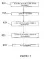
- FIG. 3is a flowchart detailing shows, in accordance with one embodiment of the present invention, the formation of multi-level coplanar metal/insulator films using dual damascene techniques with sacrificial flowable oxide.
- the inventionrelates to an improved method for forming multi-level coplanar metal/insulator films.
- dual damascene with sacrificial flowable oxideis used to form an overlying metallization layer substantially simultaneously with electrical interconnections to an underlying device layer.
- a viais formed through an insulator layer to an underlying device layer using a dual damascene etch with flowable oxide.
- a trench suitable for deposition of metalis then formed in the top surface of the insulator layer positioned over the underlying device layer.
- a layer of flowable oxidethen covers the top surface of the insulator layer and is then planarized to about a level of the top of the insulator layer.
- planarization of the flowable oxideforms a substantially planar surface which is amenable to both photolithographic resolution of small surface geometries and easy removal of subsequently deposited photolithographic material.
- the viais then formed by etching through the flowable oxide within the trench and through the insulating material at the bottom of the trench to the underlying device layer.
- FIG. 2Aillustrates a cross sectional view of a structure 400 in accordance with one embodiment of the present invention.
- the structurecomprises a substrate 412 , such as silicon wafer.
- Other semiconductor substratessuch as gallium arsenide, germanium, silicon on insulator (SOI), or other semiconductor materials are also useful.
- the substratefor example, may be lightly or heavily doped with dopants of a pre-determined conductivity to achieve a desired electrical characteristics.
- the structurefor example, represents a structure employed to fabricate devices such as transistors including nFETs or pFETs (field effect transistors) and other devices including capacitors and resistors. Such devices, for example, are interconnected to form an integrated circuit (IC).
- ICintegrated circuit
- Such ICincludes a random access memory (RAM), a dynamic random access memory (DRAM), a synchronous DRAM (SDRAM), and a read only memory (ROM).
- Other IC that is formedincludes an application specific integrated circuit (ASIC) or any logic circuit.
- ASICapplication specific integrated circuit
- a plurality of ICsare formed on the wafer in parallel. After processing is finish, the wafer is diced to separate the ICs to individual chips. The chips are then packaged, resulting in a final product that is used in, for example, consumer products such as computer systems, cellular phones, personal digital assistants (PDAs), and other products.
- PDAspersonal digital assistants
- the inventionis described in the context of forming an IC for ease of understanding. Further, the IC can be in any stage of processing.
- the substrateincludes features (not shown) formed in/on the substrate.
- the featurescorrespond to devices that form an IC.
- a previously defined device layer 416wherein contact with another conductive layer is desired.
- the device layeris isolated from other device layers or features by a dielectric material, which are planarized to result in a planar surface 413 .
- Device layer 416represents a portion of an underlying metallization layer.
- the device layeris a highly doped silicon, polysilicon layer, or a portion of any type of an active device such, for example, the source or drain region of a transistor.
- device layer 416represents a bitline of a DRAM IC.
- the insulator layer 418is provided over surface 413 .
- the insulator layercomprises a dielectric material such as silicon oxide.
- Other materialssuch as doped silicate glass including phosphosilicate glass (PSG), borosilicate glass (BSG), or borophoshosilciate glass (BPSG).
- Other insulator materialalso includes, for example, a polymer like polyimide.
- the insulator layercan be deposited on the substrate by, for example, chemical vapor deposition (CVD) or other deposition techniques.
- the insulator layer 418may have a thickness in the range of about 0.9 to 2.0 microns. To provide a planar top surface, the insulator layer is typically planarized.
- lithographic techniquesare employed to patterned the insulator layer to form a first trench 404 .
- Such techniquesinclude depositing ARC and photoresist layers 513 and 500 , respectively, on the surface of the wafer, covering the insulator layer.
- the resist layeris selectively exposed with radiation, such as deep ultra-violet (DUV) or extreme ultra violet (EUV) from an exposure source.
- radiationsuch as deep ultra-violet (DUV) or extreme ultra violet (EUV) from an exposure source.
- DUVdeep ultra-violet
- EUVextreme ultra violet
- Other exposure sources generating radiation having wavelengths that are different from DUV and EUVare also useful.
- the exposed or unexposed portion of the resist layeris removed during development to expose a portion of the insulator layer corresponding to trench 404 .
- the waferis then etched anisotropically in an etch chamber to form the trench.
- An anisotropic etch processfor example, includes reactive ion etching (RIE).
- RIEreactive ion etching
- a first anisotropic etch processis utilized to breaks through the organic ARC layer.
- An etchantsuch as N 2 can be used to etch the ARC layer.
- a second anisotropic etchremoves a desired amount of insulator material to create the trench.
- C 4 F 8 and O 2for example are used as etchant source gases to etch the insulator layer.
- trench 404represents an overlying metallization layer that is to be contacted with underlying device layer 416 .
- the overlying metallizationfor example, is a conductive line.
- the conductive lineis electrically connected to device layer 416 by a subsequently formed via hole, which will be discussed later.
- the conductive layeris to be contacted with region 416 .
- the position of trench 410is above region 416 .
- Other trenches, such as trench 410representing conductive lines are located over other defined regions with which electrical contact is desired.
- the depth and width of the trenchesdepend on the design parameters, such as sheet resistance and materials used. Typically, the etch is timed to achieve the desired depth.
- a second insulator layer(not shown) is deposited over the insulator layer 418 .
- the second insulatorcomprises, for example, a dielectric which is different from the first insulator material and can be etched selective thereto. This allows the first insulator material to serve as an etch stop, thereby defining the depth of the trench. As such, the first insulator material need not be as thick, while the second insulator layer has a thickness equal to about the thickness of the conductive line defined by the trenches.
- a layer of flowable oxide 400referred to as spin on glass (SOG) is deposited upon the upper surface 406 of insulator 418 .
- flowable oxideis a polymeric compound that forms SiO 2 .
- the flowable oxidefor example, is FOx which is manufactured by Corning. Other flowable oxides and SOGs are also useful.
- FOxis used to fill the trenches.
- the FOxis deposited by a spin on process or by any other conventional deposition techniques.
- the flowable oxidemay be formed by coating the substrate with a layer of hydrogen silesquioxane in a conventional SOG spin coater. In one case, the coating material may be spun on at about 1000-5000 RPM while baking the substrate in a sequence of about 150° C. for about one minute, about 250° C. for about one minute, and about 350° C. for about one minute.
- the layer 400is sufficiently thick to fill the trenches.
- the flowable oxidefor example, extends approximately to at least a desired thickness “h” above the upper surface 406 of insulator 418 .
- hdepends on process control parameters.
- layer 400may be about 500 nm thick in some cases.
- the flowable oxide layer 400is then etched back so as to be substantially coplanar to the upper surface 406 of the insulator 418 .
- the upper surface 406 of insulator 418is used as an etch stop.
- a substantially planar surface 402is formed covering trench 404 substantially simultaneously with a substantially planar surface 408 that covers trench 410 .
- the upper surface 406 of insulator 418 together with the surfaces 402 and 408present a substantially planar surface suitable for resolution of small surface geometries using photolithography.
- forming a via suitable for interconnecting an underlying device layer and an overlying metallization through an insulator layermay include the following operations. First depositing an ARC layer 513 (which is typically organic in nature) and a photoresist layer 500 on the upper surface 406 of insulator 418 and surfaces 402 and 408 . Next, the photoresist layer 500 is developed by methods well known in the art in preparation for etching the flowable oxide within the previously existing trench 404 and insulator 418 at the bottom of previously existing trench 404 to form via hole 508 .
- ARC layer 513which is typically organic in nature
- the organic ARC layer 513may be etched by placing the wafer in an oxide etch chamber where a first etch process known in the art as RIE utilizing N 2 etchant source gas breaks through the organic ARC layer 513 in the areas exposed by the developed photoresist.
- a first etch process known in the art as RIE utilizing N 2 etchant source gasbreaks through the organic ARC layer 513 in the areas exposed by the developed photoresist.
- the via hole 508is formed by etching through the flowable oxide 506 included in previously existing trench 404 using C 4 F 8 etchant source gas and a first quantity of O 2 etchant source gas followed by etching through insulator 418 using C 4 F 8 etchant source gas and the second quantity of O 2 etchant source gas using device layer 416 as an etch stop.
- the first quantity of O 2 etchant source gasmay be greater than the second quantity of O 2 etchant source gas.
- the flowable oxide within previously existing trench 410may be removed in a similar manner using insulator 518 as an etch stop.
- the flowable oxideis removed by etching the substrate via a RIE etch using, for example, Ar, C 4 F 8 , CO and/or O 2 .
- FIG. 2Dillustrates a cross sectional view of a semiconductor structure 400 in accordance with one embodiment of the present invention after completion of the formation of via hole 508 .
- the flowable oxide within trench 410 and trench 404has been removed, as are the ARC layer and the via etch photoresist mask.
- the metalsmay be deposited by known techniques such as chemical vapor deposition (CVD), physical vapor deposition (PVD), or low pressure chemical vapor deposition (LPCVD).
- CVDchemical vapor deposition
- PVDphysical vapor deposition
- LPCVDlow pressure chemical vapor deposition
- CVDchemical vapor deposition
- PVDphysical vapor deposition
- LPCVDlow pressure chemical vapor deposition
- Deposition of the metal(usually in blanket fashion over the entire surface of the semiconductor structure) fills trench 410 and via hole 508 thereby substantially simultaneously forming the overlying metallization and associated via interconnects to the underlying device layer 416 .
- the formation of multi-level coplanar metal/insulator films using dual damascene techniques with sacrificial flowable oxidewhich is detailed in the flowchart illustrated by FIG. 3 may include, in one embodiment of the present invention, the following operative steps.
- a substrate with a layer stack disposed above the substrateis provided.
- the layer stackincludes an underlying device layer and an insulating layer disposed above said underlying device layer.
- the substrateis shown as substrate 412 and the underlying device layer is shown as device layer 416 .
- Insulator layer 418is shown disposed above the substrate and the underlying device layer 416 .
- a trenchis formed in the top surface of the insulator layer.
- the trenchis positioned above the underlying device layer with the insulator layer disposed between the bottom of trench and the underlying device layer.
- the trenchis shown as trench 404 .
- a layer of flowable oxideis deposited over the top surface of the insulator layer.
- This flowable oxideis shown in FIG. 2A as flowable oxide 400 .
- flowable oxideis a polymeric compound that forms SiO 2 .
- the depositionmay be performed by a spin on process or by any other conventional means known by those skilled in the art.
- step 825the layer of flowable oxide is planarized down to about a level of the top surface of insulator layer as shown in FIG. 2 B. In some cases, however, it is permissible to planarize even further, e.g., beyond the level of the previously existing top surface of the insulating layer.
- FIG. 2Cillustrates how in step 830 a via 508 is formed by etching through the flowable oxide within trench 404 and the insulator layer 418 at the bottom of trench 404 down to the underlying device layer 416 .
- Another advantage of the inventionrelates to the fact that the flowable oxide surface is planarized prior to depositing the ARC layer. Since the ability of photolithography to adequately resolve small geometries is related to the planarity of the surface upon which the ARC deposition occurs, it is advantageous to have as planar a surface as is possible. As described, the flowable oxide permits a planar surface to be formed which, in contrast to conventional dual damascene techniques, facilitates the resolution of small geometries without investing in the best optical or electron beam lithography equipment available.
Landscapes
- Engineering & Computer Science (AREA)
- Physics & Mathematics (AREA)
- Condensed Matter Physics & Semiconductors (AREA)
- General Physics & Mathematics (AREA)
- Manufacturing & Machinery (AREA)
- Computer Hardware Design (AREA)
- Microelectronics & Electronic Packaging (AREA)
- Power Engineering (AREA)
- Internal Circuitry In Semiconductor Integrated Circuit Devices (AREA)
- Drying Of Semiconductors (AREA)
- Electrodes Of Semiconductors (AREA)
Abstract
Description
Claims (23)
Priority Applications (7)
| Application Number | Priority Date | Filing Date | Title |
|---|---|---|---|
| US08/884,861US6300235B1 (en) | 1997-06-30 | 1997-06-30 | Method of forming multi-level coplanar metal/insulator films using dual damascene with sacrificial flowable oxide |
| EP98110307AEP0895283B1 (en) | 1997-06-30 | 1998-06-05 | Method of forming multi-level coplanar metal/insulator films using dual damascene with sacrificial flowable oxide |
| DE69837313TDE69837313T2 (en) | 1997-06-30 | 1998-06-05 | A method of making coplanar metal / insulating multilayer films using a damascene sacrificial oxide flow process |
| TW087109645ATW462112B (en) | 1997-06-30 | 1998-06-17 | Method of forming multi-level coplanar metal/insulator films using dual damascene with sacrificial flowable oxide |
| KR10-1998-0023337AKR100494955B1 (en) | 1997-06-30 | 1998-06-22 | Method of forming multi-level coplanar metal/insulator films using dual damascene with sacrificial flowable oxide |
| CNB981156274ACN1146956C (en) | 1997-06-30 | 1998-06-30 | Method of forming multi-level coplanar metal/insulator films using dual damascene with sacrificial flowable oxide |
| JP10184376AJPH1187352A (en) | 1997-06-30 | 1998-06-30 | Method of performing dual damascene etching and method of forming via |
Applications Claiming Priority (1)
| Application Number | Priority Date | Filing Date | Title |
|---|---|---|---|
| US08/884,861US6300235B1 (en) | 1997-06-30 | 1997-06-30 | Method of forming multi-level coplanar metal/insulator films using dual damascene with sacrificial flowable oxide |
Publications (1)
| Publication Number | Publication Date |
|---|---|
| US6300235B1true US6300235B1 (en) | 2001-10-09 |
Family
ID=25385585
Family Applications (1)
| Application Number | Title | Priority Date | Filing Date |
|---|---|---|---|
| US08/884,861Expired - LifetimeUS6300235B1 (en) | 1997-06-30 | 1997-06-30 | Method of forming multi-level coplanar metal/insulator films using dual damascene with sacrificial flowable oxide |
Country Status (7)
| Country | Link |
|---|---|
| US (1) | US6300235B1 (en) |
| EP (1) | EP0895283B1 (en) |
| JP (1) | JPH1187352A (en) |
| KR (1) | KR100494955B1 (en) |
| CN (1) | CN1146956C (en) |
| DE (1) | DE69837313T2 (en) |
| TW (1) | TW462112B (en) |
Cited By (21)
| Publication number | Priority date | Publication date | Assignee | Title |
|---|---|---|---|---|
| US6372635B1 (en)* | 2001-02-06 | 2002-04-16 | Advanced Micro Devices, Inc. | Method for making a slot via filled dual damascene low k interconnect structure without middle stop layer |
| US6444570B2 (en)* | 2000-03-13 | 2002-09-03 | Kabushiki Kaisha Toshiba | Method of manufacturing a multi-layered wiring structure for interconnecting semiconductor devices by patterning resist and antireflective films to define wiring grooves |
| US6465358B1 (en)* | 2000-10-06 | 2002-10-15 | Intel Corporation | Post etch clean sequence for making a semiconductor device |
| US6521542B1 (en)* | 2000-06-14 | 2003-02-18 | International Business Machines Corp. | Method for forming dual damascene structure |
| US6576550B1 (en)* | 2000-06-30 | 2003-06-10 | Infineon, Ag | ‘Via first’ dual damascene process for copper metallization |
| US20030199169A1 (en)* | 2002-04-17 | 2003-10-23 | Samsung Electronics Co., Ltd. | Method of forming dual damascene interconnection using low-k dielectric |
| US20030211727A1 (en)* | 2002-05-13 | 2003-11-13 | Nanya Technology Corporation | Dual damascene process |
| US6680254B2 (en)* | 2001-02-27 | 2004-01-20 | Nanya Technology Corporation | Method of fabricating bit line and bit line contact plug of a memory cell |
| US20040067634A1 (en)* | 2002-05-28 | 2004-04-08 | Samsung Electronics Co., Ltd. | Method of forming dual damascene interconnection using low-k dielectric material |
| US6720252B2 (en)* | 2002-07-30 | 2004-04-13 | Promos Technologies, Inc. | Method of deep contact fill and planarization for dual damascene structures |
| US6727143B1 (en)* | 1999-11-30 | 2004-04-27 | Advanced Micro Devices, Inc. | Method and system for reducing charge gain and charge loss when using an ARC layer in interlayer dielectric formation |
| US6753208B1 (en) | 1998-03-20 | 2004-06-22 | Mcsp, Llc | Wafer scale method of packaging integrated circuit die |
| KR100442147B1 (en)* | 2002-08-09 | 2004-07-27 | 동부전자 주식회사 | Method for forming dual damascene pattern |
| US20050106856A1 (en)* | 2003-11-14 | 2005-05-19 | Taiwan Semiconductor Manufacturing Co. | Dual damascene process flow for porous low-k materials |
| US7205181B1 (en) | 1998-03-20 | 2007-04-17 | Mcsp, Llc | Method of forming hermetic wafer scale integrated circuit structure |
| US7215025B1 (en)* | 1998-03-20 | 2007-05-08 | Mcsp, Llc | Wafer scale semiconductor structure |
| US20090239375A1 (en)* | 2008-03-19 | 2009-09-24 | Philipp Riess | Dual Damascene Process |
| US20090275185A1 (en)* | 2008-05-02 | 2009-11-05 | Kevin Shea | Methods of forming capacitors |
| US20090275187A1 (en)* | 2008-05-02 | 2009-11-05 | Mark Kiehlbauch | Methods of forming capacitors |
| US7863654B2 (en) | 1998-12-21 | 2011-01-04 | Megica Corporation | Top layers of metal for high performance IC's |
| US20180358363A1 (en)* | 2017-03-01 | 2018-12-13 | United Microelectronics Corp. | Semiconductor structure, semiconductor structure for memory device and method for forming the same |
Families Citing this family (9)
| Publication number | Priority date | Publication date | Assignee | Title |
|---|---|---|---|---|
| JP3214475B2 (en)* | 1998-12-21 | 2001-10-02 | 日本電気株式会社 | Method of forming dual damascene wiring |
| JP3704030B2 (en)* | 2000-07-24 | 2005-10-05 | シャープ株式会社 | Manufacturing method of semiconductor device |
| US6514860B1 (en)* | 2001-01-31 | 2003-02-04 | Advanced Micro Devices, Inc. | Integration of organic fill for dual damascene process |
| KR100405934B1 (en)* | 2001-12-26 | 2003-11-14 | 주식회사 하이닉스반도체 | Method for manufacturing a contact hole of semiconductor device |
| US6955926B2 (en)* | 2004-02-25 | 2005-10-18 | International Business Machines Corporation | Method of fabricating data tracks for use in a magnetic shift register memory device |
| KR100624098B1 (en) | 2005-06-16 | 2006-09-15 | 삼성전자주식회사 | Thin film structure and formation method thereof |
| KR100703560B1 (en)* | 2005-12-28 | 2007-04-03 | 동부일렉트로닉스 주식회사 | Metal wiring formation method of semiconductor device |
| CN102592989B (en)* | 2011-01-07 | 2015-04-08 | 中国科学院微电子研究所 | Near-interface planarization back-etching method for interlayer dielectric |
| US8629037B2 (en)* | 2011-09-24 | 2014-01-14 | Taiwan Semiconductor Manufacturing Company, Ltd. | Forming a protective film on a back side of a silicon wafer in a III-V family fabrication process |
Citations (7)
| Publication number | Priority date | Publication date | Assignee | Title |
|---|---|---|---|---|
| US5444020A (en) | 1992-10-13 | 1995-08-22 | Samsung Electronics Co., Ltd. | Method for forming contact holes having different depths |
| US5449644A (en)* | 1994-01-13 | 1995-09-12 | United Microelectronics Corporation | Process for contact hole formation using a sacrificial SOG layer |
| EP0726596A2 (en) | 1995-02-07 | 1996-08-14 | Tokyo Electron Limited | Plasma etching method |
| EP0763850A1 (en) | 1995-09-01 | 1997-03-19 | Applied Materials, Inc. | Etch process for forming contacts over a silicide layer |
| US5614765A (en)* | 1995-06-07 | 1997-03-25 | Advanced Micro Devices, Inc. | Self aligned via dual damascene |
| US5733712A (en)* | 1995-02-20 | 1998-03-31 | Hitachi, Ltd. | Resist pattern forming method using anti-reflective layer, resist pattern formed, and method of etching using resist pattern and product formed |
| US6686354B2 (en)* | 1998-12-18 | 2004-02-03 | Scios, Inc. | Agonists and antagonists of peripheral-type benzodiazepine receptors |
- 1997
- 1997-06-30USUS08/884,861patent/US6300235B1/ennot_activeExpired - Lifetime
- 1998
- 1998-06-05DEDE69837313Tpatent/DE69837313T2/ennot_activeExpired - Lifetime
- 1998-06-05EPEP98110307Apatent/EP0895283B1/ennot_activeExpired - Lifetime
- 1998-06-17TWTW087109645Apatent/TW462112B/ennot_activeIP Right Cessation
- 1998-06-22KRKR10-1998-0023337Apatent/KR100494955B1/ennot_activeExpired - Fee Related
- 1998-06-30CNCNB981156274Apatent/CN1146956C/ennot_activeExpired - Fee Related
- 1998-06-30JPJP10184376Apatent/JPH1187352A/enactivePending
Patent Citations (7)
| Publication number | Priority date | Publication date | Assignee | Title |
|---|---|---|---|---|
| US5444020A (en) | 1992-10-13 | 1995-08-22 | Samsung Electronics Co., Ltd. | Method for forming contact holes having different depths |
| US5449644A (en)* | 1994-01-13 | 1995-09-12 | United Microelectronics Corporation | Process for contact hole formation using a sacrificial SOG layer |
| EP0726596A2 (en) | 1995-02-07 | 1996-08-14 | Tokyo Electron Limited | Plasma etching method |
| US5733712A (en)* | 1995-02-20 | 1998-03-31 | Hitachi, Ltd. | Resist pattern forming method using anti-reflective layer, resist pattern formed, and method of etching using resist pattern and product formed |
| US5614765A (en)* | 1995-06-07 | 1997-03-25 | Advanced Micro Devices, Inc. | Self aligned via dual damascene |
| EP0763850A1 (en) | 1995-09-01 | 1997-03-19 | Applied Materials, Inc. | Etch process for forming contacts over a silicide layer |
| US6686354B2 (en)* | 1998-12-18 | 2004-02-03 | Scios, Inc. | Agonists and antagonists of peripheral-type benzodiazepine receptors |
Non-Patent Citations (2)
| Title |
|---|
| Peter Singer: "Making the Move to Dual Damascene Processing" Semiconductor International, vol. 20, No. 9, Aug. 1997 (pp. 79-82). |
| S. Wolf and R. Tauber "Silicon Processing for the VLSI Era vol. I." (Lattice Press, Calif.) pp. 546-551, 1986.* |
Cited By (48)
| Publication number | Priority date | Publication date | Assignee | Title |
|---|---|---|---|---|
| US6753208B1 (en) | 1998-03-20 | 2004-06-22 | Mcsp, Llc | Wafer scale method of packaging integrated circuit die |
| US7205635B1 (en) | 1998-03-20 | 2007-04-17 | Mcsp, Llc | Hermetic wafer scale integrated circuit structure |
| US7205181B1 (en) | 1998-03-20 | 2007-04-17 | Mcsp, Llc | Method of forming hermetic wafer scale integrated circuit structure |
| US6982475B1 (en) | 1998-03-20 | 2006-01-03 | Mcsp, Llc | Hermetic wafer scale integrated circuit structure |
| US7215025B1 (en)* | 1998-03-20 | 2007-05-08 | Mcsp, Llc | Wafer scale semiconductor structure |
| US8471384B2 (en) | 1998-12-21 | 2013-06-25 | Megica Corporation | Top layers of metal for high performance IC's |
| US8415800B2 (en) | 1998-12-21 | 2013-04-09 | Megica Corporation | Top layers of metal for high performance IC's |
| US7863654B2 (en) | 1998-12-21 | 2011-01-04 | Megica Corporation | Top layers of metal for high performance IC's |
| US8531038B2 (en) | 1998-12-21 | 2013-09-10 | Megica Corporation | Top layers of metal for high performance IC's |
| US7884479B2 (en) | 1998-12-21 | 2011-02-08 | Megica Corporation | Top layers of metal for high performance IC's |
| US7999384B2 (en) | 1998-12-21 | 2011-08-16 | Megica Corporation | Top layers of metal for high performance IC's |
| US8022545B2 (en) | 1998-12-21 | 2011-09-20 | Megica Corporation | Top layers of metal for high performance IC's |
| US6727143B1 (en)* | 1999-11-30 | 2004-04-27 | Advanced Micro Devices, Inc. | Method and system for reducing charge gain and charge loss when using an ARC layer in interlayer dielectric formation |
| US6444570B2 (en)* | 2000-03-13 | 2002-09-03 | Kabushiki Kaisha Toshiba | Method of manufacturing a multi-layered wiring structure for interconnecting semiconductor devices by patterning resist and antireflective films to define wiring grooves |
| US6521542B1 (en)* | 2000-06-14 | 2003-02-18 | International Business Machines Corp. | Method for forming dual damascene structure |
| US6576550B1 (en)* | 2000-06-30 | 2003-06-10 | Infineon, Ag | ‘Via first’ dual damascene process for copper metallization |
| US6465358B1 (en)* | 2000-10-06 | 2002-10-15 | Intel Corporation | Post etch clean sequence for making a semiconductor device |
| US6603206B2 (en) | 2001-02-06 | 2003-08-05 | Advanced Micro Devices, Inc. | Slot via filled dual damascene interconnect structure without middle etch stop layer |
| US6372635B1 (en)* | 2001-02-06 | 2002-04-16 | Advanced Micro Devices, Inc. | Method for making a slot via filled dual damascene low k interconnect structure without middle stop layer |
| US6680254B2 (en)* | 2001-02-27 | 2004-01-20 | Nanya Technology Corporation | Method of fabricating bit line and bit line contact plug of a memory cell |
| US20030199169A1 (en)* | 2002-04-17 | 2003-10-23 | Samsung Electronics Co., Ltd. | Method of forming dual damascene interconnection using low-k dielectric |
| US6911397B2 (en) | 2002-04-17 | 2005-06-28 | Samsung Electronics, Co., Ltd. | Method of forming dual damascene interconnection using low-k dielectric |
| US20030211727A1 (en)* | 2002-05-13 | 2003-11-13 | Nanya Technology Corporation | Dual damascene process |
| US6818547B2 (en)* | 2002-05-13 | 2004-11-16 | Nanya Technology Corporation | Dual damascene process |
| US7022600B2 (en) | 2002-05-28 | 2006-04-04 | Samsung Electronics, Co., Ltd. | Method of forming dual damascene interconnection using low-k dielectric material |
| KR100454130B1 (en)* | 2002-05-28 | 2004-10-26 | 삼성전자주식회사 | Method of forming dual damascene interconnection using low dielectric material |
| US20040067634A1 (en)* | 2002-05-28 | 2004-04-08 | Samsung Electronics Co., Ltd. | Method of forming dual damascene interconnection using low-k dielectric material |
| US6720252B2 (en)* | 2002-07-30 | 2004-04-13 | Promos Technologies, Inc. | Method of deep contact fill and planarization for dual damascene structures |
| KR100442147B1 (en)* | 2002-08-09 | 2004-07-27 | 동부전자 주식회사 | Method for forming dual damascene pattern |
| US7538025B2 (en) | 2003-11-14 | 2009-05-26 | Taiwan Semiconductor Manufacturing Company | Dual damascene process flow for porous low-k materials |
| US20050106856A1 (en)* | 2003-11-14 | 2005-05-19 | Taiwan Semiconductor Manufacturing Co. | Dual damascene process flow for porous low-k materials |
| US20090239375A1 (en)* | 2008-03-19 | 2009-09-24 | Philipp Riess | Dual Damascene Process |
| US8062971B2 (en)* | 2008-03-19 | 2011-11-22 | Infineon Technologies Ag | Dual damascene process |
| US8860225B2 (en) | 2008-03-19 | 2014-10-14 | Infineon Technologies Ag | Devices formed with dual damascene process |
| US20090275187A1 (en)* | 2008-05-02 | 2009-11-05 | Mark Kiehlbauch | Methods of forming capacitors |
| US20090275185A1 (en)* | 2008-05-02 | 2009-11-05 | Kevin Shea | Methods of forming capacitors |
| US7696056B2 (en) | 2008-05-02 | 2010-04-13 | Micron Technology, Inc. | Methods of forming capacitors |
| US8241987B2 (en) | 2008-05-02 | 2012-08-14 | Micron Technology, Inc. | Methods of forming capacitors |
| US8318578B2 (en) | 2008-05-02 | 2012-11-27 | Micron Technology, Inc. | Method of forming capacitors |
| US7618874B1 (en) | 2008-05-02 | 2009-11-17 | Micron Technology, Inc. | Methods of forming capacitors |
| US20100159667A1 (en)* | 2008-05-02 | 2010-06-24 | Micron Technology, Inc. | Methods of Forming Capacitors |
| US20100025362A1 (en)* | 2008-05-02 | 2010-02-04 | Micron Technology, Inc. | Method of Forming Capacitors |
| US8623725B2 (en) | 2008-05-02 | 2014-01-07 | Micron Technology, Inc. | Methods of forming capacitors |
| US7964471B2 (en) | 2008-05-02 | 2011-06-21 | Micron Technology, Inc. | Methods of forming capacitors |
| US20180358363A1 (en)* | 2017-03-01 | 2018-12-13 | United Microelectronics Corp. | Semiconductor structure, semiconductor structure for memory device and method for forming the same |
| US10903215B2 (en) | 2017-03-01 | 2021-01-26 | United Microelectronics Corp. | Layout structure of semiconductor structure for dynamic random access memory device and method for forming the same |
| US11943911B2 (en)* | 2017-03-01 | 2024-03-26 | United Microelectronics Corp. | DRAM with buried gate structure |
| US12317474B2 (en) | 2017-03-01 | 2025-05-27 | United Microelectronics Corp. | Method for forming memory device with buried gate in peripheral circuit region |
Also Published As
| Publication number | Publication date |
|---|---|
| JPH1187352A (en) | 1999-03-30 |
| KR19990007191A (en) | 1999-01-25 |
| DE69837313D1 (en) | 2007-04-26 |
| CN1146956C (en) | 2004-04-21 |
| CN1208949A (en) | 1999-02-24 |
| EP0895283B1 (en) | 2007-03-14 |
| DE69837313T2 (en) | 2007-12-20 |
| EP0895283A3 (en) | 2000-05-03 |
| TW462112B (en) | 2001-11-01 |
| EP0895283A2 (en) | 1999-02-03 |
| KR100494955B1 (en) | 2005-09-09 |
Similar Documents
| Publication | Publication Date | Title |
|---|---|---|
| US6300235B1 (en) | Method of forming multi-level coplanar metal/insulator films using dual damascene with sacrificial flowable oxide | |
| US6140238A (en) | Self-aligned copper interconnect structure and method of manufacturing same | |
| US6033977A (en) | Dual damascene structure | |
| US5480837A (en) | Process of making an integrated circuit having a planar conductive layer | |
| US5723381A (en) | Formation of self-aligned overlapping bitline contacts with sacrificial polysilicon fill-in stud | |
| US5977599A (en) | Formation of a metal via using a raised metal plug structure | |
| US6030896A (en) | Self-aligned copper interconnect architecture with enhanced copper diffusion barrier | |
| US6010955A (en) | Electrical connection forming process for semiconductor devices | |
| US6080664A (en) | Method for fabricating a high aspect ratio stacked contact hole | |
| KR100338958B1 (en) | Method for forming a capacitor of a semiconductor device | |
| JPH11163143A (en) | Method for performing dual damascene etching, method for forming via, and method for manufacturing self-aligned via | |
| KR100256057B1 (en) | Manufacturing Method of Semiconductor Device for Bit Line Capping of Ultra Fine Line Width | |
| US6066526A (en) | Method of making trench DRAM | |
| HK1016342A (en) | Method of forming multi-level coplanar metal/insulator films using dual damascene with sacreficial flowable oxide | |
| KR20000072897A (en) | method of manufacturing semiconductor device | |
| JPH10223897A (en) | Semiconductor device and manufacturing method thereof | |
| JPH11186274A (en) | Dual damascene technology | |
| KR20030040461A (en) | Semiconductor interconnection structure and method of fabrication | |
| US7799676B2 (en) | Method of manufacturing a contact structure to avoid open issue | |
| KR100524928B1 (en) | Method for forming a metal line using damascene process | |
| KR100506050B1 (en) | Contact formation method of semiconductor device | |
| US20070010089A1 (en) | Method of forming bit line of semiconductor device | |
| JPH02114549A (en) | Method for forming submicron contacts using planarized conductive pillars formed on a wafer | |
| KR0172756B1 (en) | Method of forming flatted bit line | |
| KR100480573B1 (en) | Method for forming bit line of semiconductor memory device |
Legal Events
| Date | Code | Title | Description |
|---|---|---|---|
| AS | Assignment | Owner name:SIEMENS MICROELECTRONICS, INC., CALIFORNIA Free format text:ASSIGNMENT OF ASSIGNORS INTEREST;ASSIGNORS:VOLLMER, BERND;SCHNABEL, RAINER FLORIAN;REEL/FRAME:008957/0389;SIGNING DATES FROM 19971230 TO 19980105 Owner name:SIEMENS MICROELECTRONICS, INC., CALIFORNIA Free format text:ASSIGNMENT OF ASSIGNORS INTEREST;ASSIGNOR:FELDNER, KLAUS;REEL/FRAME:008956/0308 Effective date:19980104 Owner name:SIEMENS MICROELECTRONICS, INC., CALIFORNIA Free format text:ASSIGNMENT OF ASSIGNORS INTEREST;ASSIGNOR:GREWAL, VIRINDER;REEL/FRAME:008956/0242 Effective date:19980127 | |
| AS | Assignment | Owner name:SIEMENS AKTIENGESELLSCHAFT, GERMANY Free format text:ASSIGNMENT OF ASSIGNORS INTEREST;ASSIGNOR:SIEMENS MICROELECTRONICS, INC;REEL/FRAME:009171/0613 Effective date:19980206 | |
| STCF | Information on status: patent grant | Free format text:PATENTED CASE | |
| FPAY | Fee payment | Year of fee payment:4 | |
| REMI | Maintenance fee reminder mailed | ||
| FPAY | Fee payment | Year of fee payment:8 | |
| SULP | Surcharge for late payment | Year of fee payment:7 | |
| AS | Assignment | Owner name:INFINEON TECHNOLOGIES AG,GERMANY Free format text:ASSIGNMENT OF ASSIGNORS INTEREST;ASSIGNOR:SIEMENS AKTIENGESELLSCHAFT;REEL/FRAME:024120/0001 Effective date:19990331 | |
| AS | Assignment | Owner name:QIMONDA AG,GERMANY Free format text:ASSIGNMENT OF ASSIGNORS INTEREST;ASSIGNOR:INFINEON TECHNOLOGIES AG;REEL/FRAME:024195/0054 Effective date:20060425 | |
| FPAY | Fee payment | Year of fee payment:12 | |
| AS | Assignment | Owner name:INFINEON TECHNOLOGIES AG, GERMANY Free format text:ASSIGNMENT OF ASSIGNORS INTEREST;ASSIGNOR:QIMONDA AG;REEL/FRAME:035623/0001 Effective date:20141009 | |
| AS | Assignment | Owner name:POLARIS INNOVATIONS LIMITED, IRELAND Free format text:ASSIGNMENT OF ASSIGNORS INTEREST;ASSIGNOR:INFINEON TECHNOLOGIES AG;REEL/FRAME:036293/0932 Effective date:20150708 |