US6298551B1 - Methods of forming compliant interface structures with partially open interiors for coupling two electrically conductive contact areas - Google Patents
Methods of forming compliant interface structures with partially open interiors for coupling two electrically conductive contact areasDownload PDFInfo
- Publication number
- US6298551B1 US6298551B1US09/459,586US45958699AUS6298551B1US 6298551 B1US6298551 B1US 6298551B1US 45958699 AUS45958699 AUS 45958699AUS 6298551 B1US6298551 B1US 6298551B1
- Authority
- US
- United States
- Prior art keywords
- interface
- electrically conductive
- contact areas
- coupling
- contact area
- Prior art date
- Legal status (The legal status is an assumption and is not a legal conclusion. Google has not performed a legal analysis and makes no representation as to the accuracy of the status listed.)
- Expired - Lifetime
Links
- 238000000034methodMethods0.000titleclaimsdescription41
- 230000008878couplingEffects0.000titleclaimsdescription19
- 238000010168coupling processMethods0.000titleclaimsdescription19
- 238000005859coupling reactionMethods0.000titleclaimsdescription19
- 239000000463materialSubstances0.000claimsabstractdescription51
- 239000011248coating agentSubstances0.000claimsabstractdescription19
- 238000000576coating methodMethods0.000claimsabstractdescription19
- 239000004020conductorSubstances0.000claimsabstractdescription5
- 229910000679solderInorganic materials0.000claimsdescription53
- 239000000126substanceSubstances0.000claimsdescription5
- 238000007493shaping processMethods0.000claims6
- 238000001465metallisationMethods0.000abstractdescription49
- 238000007667floatingMethods0.000abstractdescription48
- 239000000758substrateSubstances0.000abstractdescription20
- 239000010410layerSubstances0.000description53
- 230000035882stressEffects0.000description17
- 239000011805ballSubstances0.000description13
- 239000002904solventSubstances0.000description9
- 238000009413insulationMethods0.000description8
- 229910052751metalInorganic materials0.000description8
- 239000002184metalSubstances0.000description8
- 229920000642polymerPolymers0.000description8
- 239000004065semiconductorSubstances0.000description7
- 238000005476solderingMethods0.000description7
- RYGMFSIKBFXOCR-UHFFFAOYSA-NCopperChemical compound[Cu]RYGMFSIKBFXOCR-UHFFFAOYSA-N0.000description5
- 239000004642PolyimideSubstances0.000description5
- 229910052802copperInorganic materials0.000description5
- 239000010949copperSubstances0.000description5
- 239000003989dielectric materialSubstances0.000description5
- 229920001721polyimidePolymers0.000description5
- 239000004593EpoxySubstances0.000description4
- 238000004519manufacturing processMethods0.000description4
- 230000008569processEffects0.000description4
- 238000000859sublimationMethods0.000description4
- 230000008022sublimationEffects0.000description4
- 230000008646thermal stressEffects0.000description4
- 230000004308accommodationEffects0.000description3
- 230000000694effectsEffects0.000description3
- 239000003292glueSubstances0.000description3
- 238000012545processingMethods0.000description3
- 230000008439repair processEffects0.000description3
- 229910001020Au alloyInorganic materials0.000description2
- KDLHZDBZIXYQEI-UHFFFAOYSA-NPalladiumChemical compound[Pd]KDLHZDBZIXYQEI-UHFFFAOYSA-N0.000description2
- RTAQQCXQSZGOHL-UHFFFAOYSA-NTitaniumChemical compound[Ti]RTAQQCXQSZGOHL-UHFFFAOYSA-N0.000description2
- 239000000853adhesiveSubstances0.000description2
- 230000001070adhesive effectEffects0.000description2
- 238000003491arrayMethods0.000description2
- 230000000712assemblyEffects0.000description2
- 238000000429assemblyMethods0.000description2
- DMFGNRRURHSENX-UHFFFAOYSA-Nberyllium copperChemical compound[Be].[Cu]DMFGNRRURHSENX-UHFFFAOYSA-N0.000description2
- 239000000919ceramicSubstances0.000description2
- 238000005229chemical vapour depositionMethods0.000description2
- 238000007598dipping methodMethods0.000description2
- 238000005516engineering processMethods0.000description2
- 238000011049fillingMethods0.000description2
- PCHJSUWPFVWCPO-UHFFFAOYSA-NgoldChemical compound[Au]PCHJSUWPFVWCPO-UHFFFAOYSA-N0.000description2
- 229910052737goldInorganic materials0.000description2
- 239000010931goldSubstances0.000description2
- 239000003353gold alloySubstances0.000description2
- MSNOMDLPLDYDME-UHFFFAOYSA-Ngold nickelChemical compound[Ni].[Au]MSNOMDLPLDYDME-UHFFFAOYSA-N0.000description2
- 238000000227grindingMethods0.000description2
- 238000010438heat treatmentMethods0.000description2
- 239000004973liquid crystal related substanceSubstances0.000description2
- 230000008018meltingEffects0.000description2
- 238000002844meltingMethods0.000description2
- 238000012986modificationMethods0.000description2
- 230000004048modificationEffects0.000description2
- 238000000059patterningMethods0.000description2
- 229920002120photoresistant polymerPolymers0.000description2
- 238000001020plasma etchingMethods0.000description2
- -1polytetrafluoroethylenePolymers0.000description2
- 229920001343polytetrafluoroethylenePolymers0.000description2
- 239000004810polytetrafluoroethyleneSubstances0.000description2
- 238000003825pressingMethods0.000description2
- 239000007787solidSubstances0.000description2
- 238000004544sputter depositionMethods0.000description2
- 239000010936titaniumSubstances0.000description2
- 229910052719titaniumInorganic materials0.000description2
- 239000002966varnishSubstances0.000description2
- JBRZTFJDHDCESZ-UHFFFAOYSA-NAsGaChemical compound[As]#[Ga]JBRZTFJDHDCESZ-UHFFFAOYSA-N0.000description1
- 229910001111Fine metalInorganic materials0.000description1
- 229910001218Gallium arsenideInorganic materials0.000description1
- ZOKXTWBITQBERF-UHFFFAOYSA-NMolybdenumChemical compound[Mo]ZOKXTWBITQBERF-UHFFFAOYSA-N0.000description1
- 239000004734Polyphenylene sulfideSubstances0.000description1
- XUIMIQQOPSSXEZ-UHFFFAOYSA-NSiliconChemical compound[Si]XUIMIQQOPSSXEZ-UHFFFAOYSA-N0.000description1
- 229910000831SteelInorganic materials0.000description1
- 239000004809TeflonSubstances0.000description1
- 229920006362Teflon®Polymers0.000description1
- 230000009471actionEffects0.000description1
- 230000003044adaptive effectEffects0.000description1
- 150000001875compoundsChemical class0.000description1
- 238000009792diffusion processMethods0.000description1
- KPUWHANPEXNPJT-UHFFFAOYSA-NdisiloxaneChemical class[SiH3]O[SiH3]KPUWHANPEXNPJT-UHFFFAOYSA-N0.000description1
- 229920001971elastomerPolymers0.000description1
- 238000009713electroplatingMethods0.000description1
- 125000003700epoxy groupChemical group0.000description1
- 230000005496eutecticsEffects0.000description1
- 239000000945fillerSubstances0.000description1
- 239000012530fluidSubstances0.000description1
- 230000004907fluxEffects0.000description1
- 239000011521glassSubstances0.000description1
- 229910010272inorganic materialInorganic materials0.000description1
- 239000011147inorganic materialSubstances0.000description1
- 239000011810insulating materialSubstances0.000description1
- 230000002452interceptive effectEffects0.000description1
- 238000002955isolationMethods0.000description1
- 238000000608laser ablationMethods0.000description1
- 238000001459lithographyMethods0.000description1
- 230000007774longtermEffects0.000description1
- 238000005259measurementMethods0.000description1
- 238000003701mechanical millingMethods0.000description1
- 239000011806microballSubstances0.000description1
- 229910052750molybdenumInorganic materials0.000description1
- 239000011733molybdenumSubstances0.000description1
- 230000003287optical effectEffects0.000description1
- 239000011368organic materialSubstances0.000description1
- 230000008520organizationEffects0.000description1
- 230000001590oxidative effectEffects0.000description1
- 229910052763palladiumInorganic materials0.000description1
- 230000003071parasitic effectEffects0.000description1
- 210000002381plasmaAnatomy0.000description1
- 239000004033plasticSubstances0.000description1
- 229920003023plasticPolymers0.000description1
- 238000007747platingMethods0.000description1
- 239000004417polycarbonateSubstances0.000description1
- 229920000515polycarbonatePolymers0.000description1
- 229920000647polyepoxidePolymers0.000description1
- 229920000069polyphenylene sulfidePolymers0.000description1
- 229910000923precious metal alloyInorganic materials0.000description1
- 238000012216screeningMethods0.000description1
- 238000000926separation methodMethods0.000description1
- 229910052710siliconInorganic materials0.000description1
- 239000010703siliconSubstances0.000description1
- HBMJWWWQQXIZIP-UHFFFAOYSA-Nsilicon carbideChemical compound[Si+]#[C-]HBMJWWWQQXIZIP-UHFFFAOYSA-N0.000description1
- 229910010271silicon carbideInorganic materials0.000description1
- 229920002379silicone rubberPolymers0.000description1
- 239000004945silicone rubberSubstances0.000description1
- 239000002356single layerSubstances0.000description1
- 239000007921spraySubstances0.000description1
- 238000009718spray depositionMethods0.000description1
- 239000010959steelSubstances0.000description1
- 238000005092sublimation methodMethods0.000description1
- BFKJFAAPBSQJPD-UHFFFAOYSA-NtetrafluoroetheneChemical compoundFC(F)=C(F)FBFKJFAAPBSQJPD-UHFFFAOYSA-N0.000description1
- 238000005979thermal decomposition reactionMethods0.000description1
- 238000011282treatmentMethods0.000description1
- WFKWXMTUELFFGS-UHFFFAOYSA-NtungstenChemical compound[W]WFKWXMTUELFFGS-UHFFFAOYSA-N0.000description1
- 229910052721tungstenInorganic materials0.000description1
- 239000010937tungstenSubstances0.000description1
- 210000002268woolAnatomy0.000description1
Images


Classifications
- H—ELECTRICITY
- H01—ELECTRIC ELEMENTS
- H01L—SEMICONDUCTOR DEVICES NOT COVERED BY CLASS H10
- H01L24/00—Arrangements for connecting or disconnecting semiconductor or solid-state bodies; Methods or apparatus related thereto
- H01L24/01—Means for bonding being attached to, or being formed on, the surface to be connected, e.g. chip-to-package, die-attach, "first-level" interconnects; Manufacturing methods related thereto
- H01L24/02—Bonding areas ; Manufacturing methods related thereto
- H—ELECTRICITY
- H01—ELECTRIC ELEMENTS
- H01L—SEMICONDUCTOR DEVICES NOT COVERED BY CLASS H10
- H01L21/00—Processes or apparatus adapted for the manufacture or treatment of semiconductor or solid state devices or of parts thereof
- H01L21/02—Manufacture or treatment of semiconductor devices or of parts thereof
- H01L21/04—Manufacture or treatment of semiconductor devices or of parts thereof the devices having potential barriers, e.g. a PN junction, depletion layer or carrier concentration layer
- H01L21/48—Manufacture or treatment of parts, e.g. containers, prior to assembly of the devices, using processes not provided for in a single one of the groups H01L21/18 - H01L21/326 or H10D48/04 - H10D48/07
- H01L21/4814—Conductive parts
- H01L21/4846—Leads on or in insulating or insulated substrates, e.g. metallisation
- H01L21/4853—Connection or disconnection of other leads to or from a metallisation, e.g. pins, wires, bumps
- H—ELECTRICITY
- H01—ELECTRIC ELEMENTS
- H01L—SEMICONDUCTOR DEVICES NOT COVERED BY CLASS H10
- H01L23/00—Details of semiconductor or other solid state devices
- H01L23/48—Arrangements for conducting electric current to or from the solid state body in operation, e.g. leads, terminal arrangements ; Selection of materials therefor
- H01L23/488—Arrangements for conducting electric current to or from the solid state body in operation, e.g. leads, terminal arrangements ; Selection of materials therefor consisting of soldered or bonded constructions
- H01L23/498—Leads, i.e. metallisations or lead-frames on insulating substrates, e.g. chip carriers
- H01L23/49811—Additional leads joined to the metallisation on the insulating substrate, e.g. pins, bumps, wires, flat leads
- H01L23/49816—Spherical bumps on the substrate for external connection, e.g. ball grid arrays [BGA]
- H—ELECTRICITY
- H01—ELECTRIC ELEMENTS
- H01L—SEMICONDUCTOR DEVICES NOT COVERED BY CLASS H10
- H01L23/00—Details of semiconductor or other solid state devices
- H01L23/48—Arrangements for conducting electric current to or from the solid state body in operation, e.g. leads, terminal arrangements ; Selection of materials therefor
- H01L23/488—Arrangements for conducting electric current to or from the solid state body in operation, e.g. leads, terminal arrangements ; Selection of materials therefor consisting of soldered or bonded constructions
- H01L23/498—Leads, i.e. metallisations or lead-frames on insulating substrates, e.g. chip carriers
- H01L23/49827—Via connections through the substrates, e.g. pins going through the substrate, coaxial cables
- H—ELECTRICITY
- H01—ELECTRIC ELEMENTS
- H01L—SEMICONDUCTOR DEVICES NOT COVERED BY CLASS H10
- H01L24/00—Arrangements for connecting or disconnecting semiconductor or solid-state bodies; Methods or apparatus related thereto
- H01L24/01—Means for bonding being attached to, or being formed on, the surface to be connected, e.g. chip-to-package, die-attach, "first-level" interconnects; Manufacturing methods related thereto
- H01L24/02—Bonding areas ; Manufacturing methods related thereto
- H01L24/04—Structure, shape, material or disposition of the bonding areas prior to the connecting process
- H01L24/05—Structure, shape, material or disposition of the bonding areas prior to the connecting process of an individual bonding area
- H—ELECTRICITY
- H01—ELECTRIC ELEMENTS
- H01L—SEMICONDUCTOR DEVICES NOT COVERED BY CLASS H10
- H01L24/00—Arrangements for connecting or disconnecting semiconductor or solid-state bodies; Methods or apparatus related thereto
- H01L24/01—Means for bonding being attached to, or being formed on, the surface to be connected, e.g. chip-to-package, die-attach, "first-level" interconnects; Manufacturing methods related thereto
- H01L24/10—Bump connectors ; Manufacturing methods related thereto
- H01L24/12—Structure, shape, material or disposition of the bump connectors prior to the connecting process
- H01L24/13—Structure, shape, material or disposition of the bump connectors prior to the connecting process of an individual bump connector
- H—ELECTRICITY
- H05—ELECTRIC TECHNIQUES NOT OTHERWISE PROVIDED FOR
- H05K—PRINTED CIRCUITS; CASINGS OR CONSTRUCTIONAL DETAILS OF ELECTRIC APPARATUS; MANUFACTURE OF ASSEMBLAGES OF ELECTRICAL COMPONENTS
- H05K3/00—Apparatus or processes for manufacturing printed circuits
- H05K3/30—Assembling printed circuits with electric components, e.g. with resistor
- H05K3/32—Assembling printed circuits with electric components, e.g. with resistor electrically connecting electric components or wires to printed circuits
- H05K3/34—Assembling printed circuits with electric components, e.g. with resistor electrically connecting electric components or wires to printed circuits by soldering
- H05K3/341—Surface mounted components
- H05K3/3431—Leadless components
- H05K3/3436—Leadless components having an array of bottom contacts, e.g. pad grid array or ball grid array components
- H—ELECTRICITY
- H01—ELECTRIC ELEMENTS
- H01L—SEMICONDUCTOR DEVICES NOT COVERED BY CLASS H10
- H01L2224/00—Indexing scheme for arrangements for connecting or disconnecting semiconductor or solid-state bodies and methods related thereto as covered by H01L24/00
- H01L2224/01—Means for bonding being attached to, or being formed on, the surface to be connected, e.g. chip-to-package, die-attach, "first-level" interconnects; Manufacturing methods related thereto
- H01L2224/02—Bonding areas; Manufacturing methods related thereto
- H01L2224/0212—Auxiliary members for bonding areas, e.g. spacers
- H01L2224/02122—Auxiliary members for bonding areas, e.g. spacers being formed on the semiconductor or solid-state body
- H01L2224/02123—Auxiliary members for bonding areas, e.g. spacers being formed on the semiconductor or solid-state body inside the bonding area
- H01L2224/02125—Reinforcing structures
- H—ELECTRICITY
- H01—ELECTRIC ELEMENTS
- H01L—SEMICONDUCTOR DEVICES NOT COVERED BY CLASS H10
- H01L2224/00—Indexing scheme for arrangements for connecting or disconnecting semiconductor or solid-state bodies and methods related thereto as covered by H01L24/00
- H01L2224/01—Means for bonding being attached to, or being formed on, the surface to be connected, e.g. chip-to-package, die-attach, "first-level" interconnects; Manufacturing methods related thereto
- H01L2224/02—Bonding areas; Manufacturing methods related thereto
- H01L2224/04—Structure, shape, material or disposition of the bonding areas prior to the connecting process
- H01L2224/0401—Bonding areas specifically adapted for bump connectors, e.g. under bump metallisation [UBM]
- H—ELECTRICITY
- H01—ELECTRIC ELEMENTS
- H01L—SEMICONDUCTOR DEVICES NOT COVERED BY CLASS H10
- H01L2224/00—Indexing scheme for arrangements for connecting or disconnecting semiconductor or solid-state bodies and methods related thereto as covered by H01L24/00
- H01L2224/01—Means for bonding being attached to, or being formed on, the surface to be connected, e.g. chip-to-package, die-attach, "first-level" interconnects; Manufacturing methods related thereto
- H01L2224/02—Bonding areas; Manufacturing methods related thereto
- H01L2224/04—Structure, shape, material or disposition of the bonding areas prior to the connecting process
- H01L2224/05—Structure, shape, material or disposition of the bonding areas prior to the connecting process of an individual bonding area
- H01L2224/0554—External layer
- H01L2224/0555—Shape
- H01L2224/05551—Shape comprising apertures or cavities
- H—ELECTRICITY
- H01—ELECTRIC ELEMENTS
- H01L—SEMICONDUCTOR DEVICES NOT COVERED BY CLASS H10
- H01L2224/00—Indexing scheme for arrangements for connecting or disconnecting semiconductor or solid-state bodies and methods related thereto as covered by H01L24/00
- H01L2224/01—Means for bonding being attached to, or being formed on, the surface to be connected, e.g. chip-to-package, die-attach, "first-level" interconnects; Manufacturing methods related thereto
- H01L2224/02—Bonding areas; Manufacturing methods related thereto
- H01L2224/04—Structure, shape, material or disposition of the bonding areas prior to the connecting process
- H01L2224/05—Structure, shape, material or disposition of the bonding areas prior to the connecting process of an individual bonding area
- H01L2224/0554—External layer
- H01L2224/0555—Shape
- H01L2224/05552—Shape in top view
- H—ELECTRICITY
- H01—ELECTRIC ELEMENTS
- H01L—SEMICONDUCTOR DEVICES NOT COVERED BY CLASS H10
- H01L2224/00—Indexing scheme for arrangements for connecting or disconnecting semiconductor or solid-state bodies and methods related thereto as covered by H01L24/00
- H01L2224/01—Means for bonding being attached to, or being formed on, the surface to be connected, e.g. chip-to-package, die-attach, "first-level" interconnects; Manufacturing methods related thereto
- H01L2224/02—Bonding areas; Manufacturing methods related thereto
- H01L2224/04—Structure, shape, material or disposition of the bonding areas prior to the connecting process
- H01L2224/05—Structure, shape, material or disposition of the bonding areas prior to the connecting process of an individual bonding area
- H01L2224/0554—External layer
- H01L2224/0555—Shape
- H01L2224/05556—Shape in side view
- H01L2224/05559—Shape in side view non conformal layer on a patterned surface
- H—ELECTRICITY
- H01—ELECTRIC ELEMENTS
- H01L—SEMICONDUCTOR DEVICES NOT COVERED BY CLASS H10
- H01L2224/00—Indexing scheme for arrangements for connecting or disconnecting semiconductor or solid-state bodies and methods related thereto as covered by H01L24/00
- H01L2224/01—Means for bonding being attached to, or being formed on, the surface to be connected, e.g. chip-to-package, die-attach, "first-level" interconnects; Manufacturing methods related thereto
- H01L2224/10—Bump connectors; Manufacturing methods related thereto
- H01L2224/12—Structure, shape, material or disposition of the bump connectors prior to the connecting process
- H01L2224/13—Structure, shape, material or disposition of the bump connectors prior to the connecting process of an individual bump connector
- H01L2224/13001—Core members of the bump connector
- H01L2224/13005—Structure
- H—ELECTRICITY
- H01—ELECTRIC ELEMENTS
- H01L—SEMICONDUCTOR DEVICES NOT COVERED BY CLASS H10
- H01L2224/00—Indexing scheme for arrangements for connecting or disconnecting semiconductor or solid-state bodies and methods related thereto as covered by H01L24/00
- H01L2224/01—Means for bonding being attached to, or being formed on, the surface to be connected, e.g. chip-to-package, die-attach, "first-level" interconnects; Manufacturing methods related thereto
- H01L2224/10—Bump connectors; Manufacturing methods related thereto
- H01L2224/12—Structure, shape, material or disposition of the bump connectors prior to the connecting process
- H01L2224/13—Structure, shape, material or disposition of the bump connectors prior to the connecting process of an individual bump connector
- H01L2224/13001—Core members of the bump connector
- H01L2224/1301—Shape
- H01L2224/13011—Shape comprising apertures or cavities, e.g. hollow bump
- H—ELECTRICITY
- H01—ELECTRIC ELEMENTS
- H01L—SEMICONDUCTOR DEVICES NOT COVERED BY CLASS H10
- H01L2224/00—Indexing scheme for arrangements for connecting or disconnecting semiconductor or solid-state bodies and methods related thereto as covered by H01L24/00
- H01L2224/01—Means for bonding being attached to, or being formed on, the surface to be connected, e.g. chip-to-package, die-attach, "first-level" interconnects; Manufacturing methods related thereto
- H01L2224/10—Bump connectors; Manufacturing methods related thereto
- H01L2224/12—Structure, shape, material or disposition of the bump connectors prior to the connecting process
- H01L2224/13—Structure, shape, material or disposition of the bump connectors prior to the connecting process of an individual bump connector
- H01L2224/13001—Core members of the bump connector
- H01L2224/13075—Plural core members
- H01L2224/13078—Plural core members being disposed next to each other, e.g. side-to-side arrangements
- H—ELECTRICITY
- H01—ELECTRIC ELEMENTS
- H01L—SEMICONDUCTOR DEVICES NOT COVERED BY CLASS H10
- H01L2224/00—Indexing scheme for arrangements for connecting or disconnecting semiconductor or solid-state bodies and methods related thereto as covered by H01L24/00
- H01L2224/01—Means for bonding being attached to, or being formed on, the surface to be connected, e.g. chip-to-package, die-attach, "first-level" interconnects; Manufacturing methods related thereto
- H01L2224/10—Bump connectors; Manufacturing methods related thereto
- H01L2224/15—Structure, shape, material or disposition of the bump connectors after the connecting process
- H01L2224/16—Structure, shape, material or disposition of the bump connectors after the connecting process of an individual bump connector
- H—ELECTRICITY
- H01—ELECTRIC ELEMENTS
- H01L—SEMICONDUCTOR DEVICES NOT COVERED BY CLASS H10
- H01L24/00—Arrangements for connecting or disconnecting semiconductor or solid-state bodies; Methods or apparatus related thereto
- H01L24/01—Means for bonding being attached to, or being formed on, the surface to be connected, e.g. chip-to-package, die-attach, "first-level" interconnects; Manufacturing methods related thereto
- H01L24/02—Bonding areas ; Manufacturing methods related thereto
- H01L24/03—Manufacturing methods
- H—ELECTRICITY
- H01—ELECTRIC ELEMENTS
- H01L—SEMICONDUCTOR DEVICES NOT COVERED BY CLASS H10
- H01L2924/00—Indexing scheme for arrangements or methods for connecting or disconnecting semiconductor or solid-state bodies as covered by H01L24/00
- H01L2924/01—Chemical elements
- H01L2924/01004—Beryllium [Be]
- H—ELECTRICITY
- H01—ELECTRIC ELEMENTS
- H01L—SEMICONDUCTOR DEVICES NOT COVERED BY CLASS H10
- H01L2924/00—Indexing scheme for arrangements or methods for connecting or disconnecting semiconductor or solid-state bodies as covered by H01L24/00
- H01L2924/01—Chemical elements
- H01L2924/01005—Boron [B]
- H—ELECTRICITY
- H01—ELECTRIC ELEMENTS
- H01L—SEMICONDUCTOR DEVICES NOT COVERED BY CLASS H10
- H01L2924/00—Indexing scheme for arrangements or methods for connecting or disconnecting semiconductor or solid-state bodies as covered by H01L24/00
- H01L2924/01—Chemical elements
- H01L2924/01006—Carbon [C]
- H—ELECTRICITY
- H01—ELECTRIC ELEMENTS
- H01L—SEMICONDUCTOR DEVICES NOT COVERED BY CLASS H10
- H01L2924/00—Indexing scheme for arrangements or methods for connecting or disconnecting semiconductor or solid-state bodies as covered by H01L24/00
- H01L2924/01—Chemical elements
- H01L2924/01013—Aluminum [Al]
- H—ELECTRICITY
- H01—ELECTRIC ELEMENTS
- H01L—SEMICONDUCTOR DEVICES NOT COVERED BY CLASS H10
- H01L2924/00—Indexing scheme for arrangements or methods for connecting or disconnecting semiconductor or solid-state bodies as covered by H01L24/00
- H01L2924/01—Chemical elements
- H01L2924/01014—Silicon [Si]
- H—ELECTRICITY
- H01—ELECTRIC ELEMENTS
- H01L—SEMICONDUCTOR DEVICES NOT COVERED BY CLASS H10
- H01L2924/00—Indexing scheme for arrangements or methods for connecting or disconnecting semiconductor or solid-state bodies as covered by H01L24/00
- H01L2924/01—Chemical elements
- H01L2924/01022—Titanium [Ti]
- H—ELECTRICITY
- H01—ELECTRIC ELEMENTS
- H01L—SEMICONDUCTOR DEVICES NOT COVERED BY CLASS H10
- H01L2924/00—Indexing scheme for arrangements or methods for connecting or disconnecting semiconductor or solid-state bodies as covered by H01L24/00
- H01L2924/01—Chemical elements
- H01L2924/01027—Cobalt [Co]
- H—ELECTRICITY
- H01—ELECTRIC ELEMENTS
- H01L—SEMICONDUCTOR DEVICES NOT COVERED BY CLASS H10
- H01L2924/00—Indexing scheme for arrangements or methods for connecting or disconnecting semiconductor or solid-state bodies as covered by H01L24/00
- H01L2924/01—Chemical elements
- H01L2924/01028—Nickel [Ni]
- H—ELECTRICITY
- H01—ELECTRIC ELEMENTS
- H01L—SEMICONDUCTOR DEVICES NOT COVERED BY CLASS H10
- H01L2924/00—Indexing scheme for arrangements or methods for connecting or disconnecting semiconductor or solid-state bodies as covered by H01L24/00
- H01L2924/01—Chemical elements
- H01L2924/01029—Copper [Cu]
- H—ELECTRICITY
- H01—ELECTRIC ELEMENTS
- H01L—SEMICONDUCTOR DEVICES NOT COVERED BY CLASS H10
- H01L2924/00—Indexing scheme for arrangements or methods for connecting or disconnecting semiconductor or solid-state bodies as covered by H01L24/00
- H01L2924/01—Chemical elements
- H01L2924/01033—Arsenic [As]
- H—ELECTRICITY
- H01—ELECTRIC ELEMENTS
- H01L—SEMICONDUCTOR DEVICES NOT COVERED BY CLASS H10
- H01L2924/00—Indexing scheme for arrangements or methods for connecting or disconnecting semiconductor or solid-state bodies as covered by H01L24/00
- H01L2924/01—Chemical elements
- H01L2924/01042—Molybdenum [Mo]
- H—ELECTRICITY
- H01—ELECTRIC ELEMENTS
- H01L—SEMICONDUCTOR DEVICES NOT COVERED BY CLASS H10
- H01L2924/00—Indexing scheme for arrangements or methods for connecting or disconnecting semiconductor or solid-state bodies as covered by H01L24/00
- H01L2924/01—Chemical elements
- H01L2924/01046—Palladium [Pd]
- H—ELECTRICITY
- H01—ELECTRIC ELEMENTS
- H01L—SEMICONDUCTOR DEVICES NOT COVERED BY CLASS H10
- H01L2924/00—Indexing scheme for arrangements or methods for connecting or disconnecting semiconductor or solid-state bodies as covered by H01L24/00
- H01L2924/01—Chemical elements
- H01L2924/01047—Silver [Ag]
- H—ELECTRICITY
- H01—ELECTRIC ELEMENTS
- H01L—SEMICONDUCTOR DEVICES NOT COVERED BY CLASS H10
- H01L2924/00—Indexing scheme for arrangements or methods for connecting or disconnecting semiconductor or solid-state bodies as covered by H01L24/00
- H01L2924/01—Chemical elements
- H01L2924/0105—Tin [Sn]
- H—ELECTRICITY
- H01—ELECTRIC ELEMENTS
- H01L—SEMICONDUCTOR DEVICES NOT COVERED BY CLASS H10
- H01L2924/00—Indexing scheme for arrangements or methods for connecting or disconnecting semiconductor or solid-state bodies as covered by H01L24/00
- H01L2924/01—Chemical elements
- H01L2924/01074—Tungsten [W]
- H—ELECTRICITY
- H01—ELECTRIC ELEMENTS
- H01L—SEMICONDUCTOR DEVICES NOT COVERED BY CLASS H10
- H01L2924/00—Indexing scheme for arrangements or methods for connecting or disconnecting semiconductor or solid-state bodies as covered by H01L24/00
- H01L2924/01—Chemical elements
- H01L2924/01078—Platinum [Pt]
- H—ELECTRICITY
- H01—ELECTRIC ELEMENTS
- H01L—SEMICONDUCTOR DEVICES NOT COVERED BY CLASS H10
- H01L2924/00—Indexing scheme for arrangements or methods for connecting or disconnecting semiconductor or solid-state bodies as covered by H01L24/00
- H01L2924/01—Chemical elements
- H01L2924/01079—Gold [Au]
- H—ELECTRICITY
- H01—ELECTRIC ELEMENTS
- H01L—SEMICONDUCTOR DEVICES NOT COVERED BY CLASS H10
- H01L2924/00—Indexing scheme for arrangements or methods for connecting or disconnecting semiconductor or solid-state bodies as covered by H01L24/00
- H01L2924/013—Alloys
- H01L2924/0132—Binary Alloys
- H01L2924/01322—Eutectic Alloys, i.e. obtained by a liquid transforming into two solid phases
- H—ELECTRICITY
- H01—ELECTRIC ELEMENTS
- H01L—SEMICONDUCTOR DEVICES NOT COVERED BY CLASS H10
- H01L2924/00—Indexing scheme for arrangements or methods for connecting or disconnecting semiconductor or solid-state bodies as covered by H01L24/00
- H01L2924/013—Alloys
- H01L2924/014—Solder alloys
- H—ELECTRICITY
- H01—ELECTRIC ELEMENTS
- H01L—SEMICONDUCTOR DEVICES NOT COVERED BY CLASS H10
- H01L2924/00—Indexing scheme for arrangements or methods for connecting or disconnecting semiconductor or solid-state bodies as covered by H01L24/00
- H01L2924/10—Details of semiconductor or other solid state devices to be connected
- H01L2924/11—Device type
- H01L2924/12—Passive devices, e.g. 2 terminal devices
- H01L2924/1204—Optical Diode
- H01L2924/12042—LASER
- H—ELECTRICITY
- H01—ELECTRIC ELEMENTS
- H01L—SEMICONDUCTOR DEVICES NOT COVERED BY CLASS H10
- H01L2924/00—Indexing scheme for arrangements or methods for connecting or disconnecting semiconductor or solid-state bodies as covered by H01L24/00
- H01L2924/19—Details of hybrid assemblies other than the semiconductor or other solid state devices to be connected
- H01L2924/1901—Structure
- H01L2924/1904—Component type
- H01L2924/19041—Component type being a capacitor
- H—ELECTRICITY
- H01—ELECTRIC ELEMENTS
- H01L—SEMICONDUCTOR DEVICES NOT COVERED BY CLASS H10
- H01L2924/00—Indexing scheme for arrangements or methods for connecting or disconnecting semiconductor or solid-state bodies as covered by H01L24/00
- H01L2924/19—Details of hybrid assemblies other than the semiconductor or other solid state devices to be connected
- H01L2924/1901—Structure
- H01L2924/1904—Component type
- H01L2924/19043—Component type being a resistor
- H—ELECTRICITY
- H01—ELECTRIC ELEMENTS
- H01L—SEMICONDUCTOR DEVICES NOT COVERED BY CLASS H10
- H01L2924/00—Indexing scheme for arrangements or methods for connecting or disconnecting semiconductor or solid-state bodies as covered by H01L24/00
- H01L2924/30—Technical effects
- H01L2924/301—Electrical effects
- H01L2924/30107—Inductance
- H—ELECTRICITY
- H01—ELECTRIC ELEMENTS
- H01L—SEMICONDUCTOR DEVICES NOT COVERED BY CLASS H10
- H01L2924/00—Indexing scheme for arrangements or methods for connecting or disconnecting semiconductor or solid-state bodies as covered by H01L24/00
- H01L2924/30—Technical effects
- H01L2924/35—Mechanical effects
- H01L2924/351—Thermal stress
- H01L2924/3511—Warping
- H—ELECTRICITY
- H05—ELECTRIC TECHNIQUES NOT OTHERWISE PROVIDED FOR
- H05K—PRINTED CIRCUITS; CASINGS OR CONSTRUCTIONAL DETAILS OF ELECTRIC APPARATUS; MANUFACTURE OF ASSEMBLAGES OF ELECTRICAL COMPONENTS
- H05K2201/00—Indexing scheme relating to printed circuits covered by H05K1/00
- H05K2201/03—Conductive materials
- H05K2201/0332—Structure of the conductor
- H05K2201/0364—Conductor shape
- H05K2201/0373—Conductors having a fine structure, e.g. providing a plurality of contact points with a structured tool
- H—ELECTRICITY
- H05—ELECTRIC TECHNIQUES NOT OTHERWISE PROVIDED FOR
- H05K—PRINTED CIRCUITS; CASINGS OR CONSTRUCTIONAL DETAILS OF ELECTRIC APPARATUS; MANUFACTURE OF ASSEMBLAGES OF ELECTRICAL COMPONENTS
- H05K2201/00—Indexing scheme relating to printed circuits covered by H05K1/00
- H05K2201/10—Details of components or other objects attached to or integrated in a printed circuit board
- H05K2201/10227—Other objects, e.g. metallic pieces
- H05K2201/10257—Hollow pieces of metal, e.g. used in connection between component and PCB
- H—ELECTRICITY
- H05—ELECTRIC TECHNIQUES NOT OTHERWISE PROVIDED FOR
- H05K—PRINTED CIRCUITS; CASINGS OR CONSTRUCTIONAL DETAILS OF ELECTRIC APPARATUS; MANUFACTURE OF ASSEMBLAGES OF ELECTRICAL COMPONENTS
- H05K2201/00—Indexing scheme relating to printed circuits covered by H05K1/00
- H05K2201/10—Details of components or other objects attached to or integrated in a printed circuit board
- H05K2201/10227—Other objects, e.g. metallic pieces
- H05K2201/10378—Interposers
- H—ELECTRICITY
- H05—ELECTRIC TECHNIQUES NOT OTHERWISE PROVIDED FOR
- H05K—PRINTED CIRCUITS; CASINGS OR CONSTRUCTIONAL DETAILS OF ELECTRIC APPARATUS; MANUFACTURE OF ASSEMBLAGES OF ELECTRICAL COMPONENTS
- H05K3/00—Apparatus or processes for manufacturing printed circuits
- H05K3/30—Assembling printed circuits with electric components, e.g. with resistor
- H05K3/32—Assembling printed circuits with electric components, e.g. with resistor electrically connecting electric components or wires to printed circuits
- H05K3/325—Assembling printed circuits with electric components, e.g. with resistor electrically connecting electric components or wires to printed circuits by abutting or pinching, i.e. without alloying process; mechanical auxiliary parts therefor
- H05K3/326—Assembling printed circuits with electric components, e.g. with resistor electrically connecting electric components or wires to printed circuits by abutting or pinching, i.e. without alloying process; mechanical auxiliary parts therefor the printed circuit having integral resilient or deformable parts, e.g. tabs or parts of flexible circuits
- H—ELECTRICITY
- H05—ELECTRIC TECHNIQUES NOT OTHERWISE PROVIDED FOR
- H05K—PRINTED CIRCUITS; CASINGS OR CONSTRUCTIONAL DETAILS OF ELECTRIC APPARATUS; MANUFACTURE OF ASSEMBLAGES OF ELECTRICAL COMPONENTS
- H05K3/00—Apparatus or processes for manufacturing printed circuits
- H05K3/40—Forming printed elements for providing electric connections to or between printed circuits
- H05K3/4092—Integral conductive tabs, i.e. conductive parts partly detached from the substrate
- Y—GENERAL TAGGING OF NEW TECHNOLOGICAL DEVELOPMENTS; GENERAL TAGGING OF CROSS-SECTIONAL TECHNOLOGIES SPANNING OVER SEVERAL SECTIONS OF THE IPC; TECHNICAL SUBJECTS COVERED BY FORMER USPC CROSS-REFERENCE ART COLLECTIONS [XRACs] AND DIGESTS
- Y02—TECHNOLOGIES OR APPLICATIONS FOR MITIGATION OR ADAPTATION AGAINST CLIMATE CHANGE
- Y02P—CLIMATE CHANGE MITIGATION TECHNOLOGIES IN THE PRODUCTION OR PROCESSING OF GOODS
- Y02P70/00—Climate change mitigation technologies in the production process for final industrial or consumer products
- Y02P70/50—Manufacturing or production processes characterised by the final manufactured product
- Y—GENERAL TAGGING OF NEW TECHNOLOGICAL DEVELOPMENTS; GENERAL TAGGING OF CROSS-SECTIONAL TECHNOLOGIES SPANNING OVER SEVERAL SECTIONS OF THE IPC; TECHNICAL SUBJECTS COVERED BY FORMER USPC CROSS-REFERENCE ART COLLECTIONS [XRACs] AND DIGESTS
- Y10—TECHNICAL SUBJECTS COVERED BY FORMER USPC
- Y10S—TECHNICAL SUBJECTS COVERED BY FORMER USPC CROSS-REFERENCE ART COLLECTIONS [XRACs] AND DIGESTS
- Y10S438/00—Semiconductor device manufacturing: process
- Y10S438/94—Laser ablative material removal
- Y—GENERAL TAGGING OF NEW TECHNOLOGICAL DEVELOPMENTS; GENERAL TAGGING OF CROSS-SECTIONAL TECHNOLOGIES SPANNING OVER SEVERAL SECTIONS OF THE IPC; TECHNICAL SUBJECTS COVERED BY FORMER USPC CROSS-REFERENCE ART COLLECTIONS [XRACs] AND DIGESTS
- Y10—TECHNICAL SUBJECTS COVERED BY FORMER USPC
- Y10T—TECHNICAL SUBJECTS COVERED BY FORMER US CLASSIFICATION
- Y10T29/00—Metal working
- Y10T29/49—Method of mechanical manufacture
- Y10T29/49002—Electrical device making
- Y10T29/49117—Conductor or circuit manufacturing
- Y10T29/49124—On flat or curved insulated base, e.g., printed circuit, etc.
- Y10T29/49126—Assembling bases
- Y—GENERAL TAGGING OF NEW TECHNOLOGICAL DEVELOPMENTS; GENERAL TAGGING OF CROSS-SECTIONAL TECHNOLOGIES SPANNING OVER SEVERAL SECTIONS OF THE IPC; TECHNICAL SUBJECTS COVERED BY FORMER USPC CROSS-REFERENCE ART COLLECTIONS [XRACs] AND DIGESTS
- Y10—TECHNICAL SUBJECTS COVERED BY FORMER USPC
- Y10T—TECHNICAL SUBJECTS COVERED BY FORMER US CLASSIFICATION
- Y10T29/00—Metal working
- Y10T29/49—Method of mechanical manufacture
- Y10T29/49002—Electrical device making
- Y10T29/49117—Conductor or circuit manufacturing
- Y10T29/49124—On flat or curved insulated base, e.g., printed circuit, etc.
- Y10T29/4913—Assembling to base an electrical component, e.g., capacitor, etc.
Definitions
- Ball grid array (BGA) technologyprovides a high density of interconnections per unit area, but mismatches of coefficients of thermal expansion (CTEs) occur when ceramic or polymer BGA substrates and printed circuit boards are joined and often result in cracked solder joints, especially as the size of the substrates and temperature ranges are increased.
- CTEscoefficients of thermal expansion
- CGAcolumn grid array
- One conventional micro ball grid array interface technique for attaching a semiconductor circuit chip directly to a substrateis to use a series of solder bumps clustered at the center of the chip to constrain the area over which stresses between differing coefficients of thermal expansion occur.
- chipshave their pads reconfigured and solder micro bumps are applied over the reconfigured pads.
- ball grid array processesare used with the temperature range being constrained during device operation to 30° C. to 70° C. in an effort to avoid CTE stress effects.
- the area where the chip faces the printed circuit board or substrateis not used for direct interconnection. Instead, metallization is routed from the chip to adjacent support structures which then have solder ball connections. This technique can create size and pin count limitations as well as electrical parasitic effects.
- a method and structure electrically interconnect materials having different coefficients of thermal expansionis used to increase reliability by providing stress and thermal accommodation of the two materials and permitting movement of the floating pad independent of the base pad.
- the inventionincludes a floating pad interface structure that is connected to a semiconductor chip's original pad by means of micro extensions that provide stress relief for different coefficients of thermal expansion.
- the floating pad interface structurescan include a single pad and extension or several extensions in situations wherein a single extension is not sufficient for extreme thermal stress/strain situations.
- the present inventionprovides a structure that accommodates thermal and material stresses without submitting the via interconnect areas to forces that can crack vias or break connections at the chip pads.
- the floating padspermit movement independent of a semiconductor while providing electrical interconnections through selected materials that are specifically patterned to provide low forces at the via areas and thus accommodate differential thermal stresses which may be caused by large CTE differences.
- a micro structure interfaceis provided that is solderable and forms an electronic interconnection without requiring pressure.
- the interconnectionscan be held in position prior to application by an interposer that provides ease of assembly and surface mount technology self-alignment capability.
- a conductive contact area interfacemay comprise: at least one electrically conductive first contact area; at least one electrically conductive second contact area facing and being substantially aligned with the at least one first contact area; and at least one interface structure coupled between the at least one first contact area and the at least one second contact area.
- the at least one interface structurecomprises at least one electrical conductor having a partially open interior to form a compliant joint between the at least one first contact area and the at least one second contact area.
- FIG. 1is a sectional side view of a compliant coating overlying a base pad.
- FIG. 2is a view similar to that of FIG. 1 further including a first interface dielectric layer.
- FIG. 3 ais a view similar to that of FIG. 2 further including floating pad structures overlying the first interface dielectric layer.
- FIG. 3 bis a view similar to that of FIG. 3 a further showing the removal of the first interface dielectric layer.
- FIG. 4is a top view of one of patterned floating pad structures overlying the base pad.
- FIGS. 5 a , 5 b , and 5 care top views of other floating pad embodiments.
- FIG. 6is a sectional side view of another floating pad embodiment.
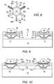
- FIG. 7is a view similar to that of FIG. 3 a further including a second interface dielectric layer and a second pair of floating pad structures overlying the first interface dielectric layer.
- FIG. 8is a top view of one of the second pair of floating pad structures.
- FIG. 9is a view similar to that of FIG. 7 further including a third interface dielectric layer having openings over the second floating pad structures for positioning of a solder bump and a solder ball and showing excess dielectric material removed.
- FIG. 10is a view similar to that of FIG. 3 a further showing a second interface dielectric layer having vias with metallization for attachment of a solder bump and solder ball.
- FIG. 11is a view similar to that of FIG. 3 a further showing a second interface dielectric layer having vias in which solder is present.
- FIG. 12is a view similar to that of FIG. 11 further including a third interface dielectric layer having openings over the solder for positioning of a solder bump and a solder ball.
- FIG. 13is a sectional side view of an interface structure for a floating pin contact.
- FIG. 14is a top view of one of the pins of FIG. 13 .
- FIG. 14 ais a sectional side view of an interface structure wherein holes do not extend all the way through an intermediate substrate.
- FIG. 15is a sectional side view of a printed circuit board and a multichip module each having area array pads.
- FIG. 16is a view similar to that of FIG. 15 further including several interface embodiments of the present invention.
- FIG. 17is a view similar to that of FIG. 16 further including an interposer embodiment of the present invention.
- FIG. 18is a schematic side view of the interface and the interposer.
- FIG. 19is a view similar to that of FIG. 18 further including solderable surfaces on the interface.
- FIG. 20is a view similar to that of FIG. 17 showing a curved base.
- FIG. 1is a sectional side view of a compliant coating 14 overlying a base surface 10 having conductive pads 12 .
- the base surfacemay comprise a semiconductor wafer that has not yet been cut into segmented individual chips or a chip which has been segmented from a wafer. Processing on a wafer that has not yet been segmented enables mass fabrication of interface structures and prevents single chip handling problems such as corner edge separations of the compliant coating and alignment difficulties associated with single die handling for photolithographic processing.
- the base surfacemay alternatively comprise, for example, a passive component, a printed circuit (PC) board, multi-chip module (MCM), a flexible interconnect layer structure such as described in Cole et al., U.S. Pat. No. 5,527,741, Jun.
- Conductive pads 12may comprise pads or metallization on any of the above-discussed base surfaces. With the present invention, interface connections for conductive pads are more stable, so the conductive pads can have smaller areas (such as a diameter or length ranging from about one mil to about four mils) than conventional pads.
- Compliant coating 14comprises a material such as a polyimide or a siloxane polyimide epoxy (SPI/epoxy) described by Gorczyca et al., U.S. Pat. No. 5,161,093, issued Nov. 3, 1992.
- the compliant coatingmay comprise a high or low modulus insulative material and typically has a thickness ranging from about two micrometers to about 100 micrometers.
- the compliant coatingcan be laminated onto base surface 10 with heat and/or an adhesive (not shown) or deposited on the base surface by a spin, spray, or chemical vapor deposition (CVD) technique, for example.
- Coating vias 16are formed in compliant coating 14 by any appropriate method.
- the compliant coatingcan be scanned repeatedly with a high energy continuous wave laser to create via holes of desired size and shape.
- Other appropriate methodsinclude, for example, photopatterning photopatternable polyimides and using an excimer laser with a mask (not shown).
- Base metallization 18can be formed by sputtering and/or plating, for example, and patterned with a standard photoresist and etch process.
- the base metallizationin one embodiment comprises a thin adhesion layer of 1000 ⁇ sputtered titanium, coated by a thin layer of 3000 ⁇ sputtered copper, coated by a layer of electroplated copper to a thickness of four microns, for example.
- An optional buffer layer of 1000 ⁇ of titaniumcan be applied over the electroplated copper.
- Other example base metallization materialsinclude molybdenum, tungsten, and gold.
- the appropriate material of the base metallizationwill vary depending on the material of the base surface and on the environment, such as a high temperature environment or an oxidizing environment for example, in which the electronic device will be used.
- FIG. 2is a view similar to that of FIG. 1 further including a first interface dielectric layer 20 which preferably comprises a flexible low modulus material, such as SPI/epoxy, other flexible epoxies, silicone rubber materials, TEFLONTM polytetrafluoroethylene (TEFLON is a trademark of E. I. du Pont de Nemours and Co.), or other polymers that have a low modulus or have been modified to obtain reduced modulus, having a thickness ranging from about two micrometers to about 3 mils. A preferred thickness range is from about 100 micrometers to about 400 micrometers.
- a flexible low modulus materialsuch as SPI/epoxy, other flexible epoxies, silicone rubber materials, TEFLONTM polytetrafluoroethylene (TEFLON is a trademark of E. I. du Pont de Nemours and Co.
- TEFLONpolytetrafluoroethylene
- a preferred thickness rangeis from about 100 micrometers to about 400 micrometers.
- First interface dielectric layer 20has vias 22 therein extending to portions of base metallization 18 overlying compliant coating 14 .
- Vias 22 of FIG. 2can be formed in a similar manner as vias 16 of FIG. 1 . If the first interface dielectric layer has a thickness less than that of the compliant coating, vias 22 can be made smaller than vias 16 , as shown.
- FIG. 3 ais a view similar to that of FIG. 2 further including floating pad structures 30 and 30 a overlying first interface dielectric layer 20
- FIG. 4is a top view of one of the floating pad structures 30 overlying the base pad.
- the floating pad structuresaccommodate thermal and material stresses without imposing undesirable forces on base metallization areas.
- Metallization for floating pad structures 30can be applied and patterned by techniques similar to those discussed with respect to base metallization 18 of FIG. 1 .
- the floating pad structuresinclude a central pad 26 having patterned extensions 28 extending through via metallization 24 to base metallization 18 .
- central pads 26will vary according to the specific planned use of the floating pad structure. For example, if a solder ball or solder bump will be attached directly to the central pad, the central pad must be large enough to accommodate the attachment. The size of the central pad will also affect the length of extensions. Smaller diameter central pads require less space than larger diameter pads and therefore leave more space for longer extensions. The area of base metallization 18 is an additional factor which can affect the available length of extensions.
- a modified central pad 26 a in FIG. 3 aincludes central pad 26 and an additional metallization area 27 .
- the extensions 28have a thickness ranging from about 2 microns to about 8 microns, and the modified central pad 26 a has a thickness ranging from about 4 microns to about 20 microns. This embodiment is useful because thin extensions are more flexible than thicker extensions whereas the central pad is preferably sufficiently thick to be solderable to another electrically conductive surface.
- the additional metallization areacomprises a metal which is readily solderable such as a nickel-gold plate, for example.
- FIG. 3 bis a view similar to that of FIG. 3 a further showing the removal of the first interface dielectric layer.
- removal of first interface dielectric layer 20is desirable so that the first interface dielectric layer does not impede the movement of MEMS devices or interfere with optical devices. Removing the first interface dielectric layer is also useful because it provides opportunities to fabricate structures having movement that can be used for measurement or control purposes.
- the material of first interface dielectric layer 20is chosen to be a material that can be removed by a sublimation process, a solvent, or a laser, for example, without interfering with compliant coating 14 .
- each area 20 a under a respective floating pad structure of FIG. 3 acan be removed with the remainder of interface dielectric layer 20 being left in position.
- the first interface dielectric layermay comprise a photosensitive material that is sensitized in regions other than in the pad regions and can thus be easily removed from under the floating pad interfaces.
- This embodimentprovides a capability of inserting an application specific filler material (which can be solid or fluid) under the floating pad interface in areas 20 a to provide special dampening (vibration) control or thermal management.
- FIGS. 5 a , 5 b , and 5 care top views of other floating pad embodiments.
- the patterning of the floating pad structure metallization shown in FIG. 4was shown for purposes of example only. Any number of extensions (one or more) can be used, and the extensions need not be straight.
- serpentine shaped extension 28 a , spiral extension 28 b , saw-tooth extension 28 c , and bent extension 28 arepresent potential shapes for purposes of example.
- central pad 526can be surrounded by extensions 528 which extend to a ring 530 which may in turn have additional extensions 532 extending to another ring 534 having vias 536 extending to base metallization 18 (not shown in FIG.
- extensions 28can be curved to form a pin-wheel shaped floating interface pad.
- the shapes of FIGS. 5 a , 5 b , and 5 ccan be useful for reducing mechanical stress on the extensions and are especially useful if base surface 10 is not planar. When selecting an extension shape, consideration of any resulting inductance effects is appropriate.
- FIG. 6is a sectional side view of another floating pad embodiment that can be useful for reducing mechanical stress on extensions.
- first interface dielectric layer 20has a dip portion 20 a which can be formed during application of the first interface dielectric layer, can be etched from the first interface dielectric layer in a separate step, or can be heat-pressed into shape.
- extensions 28will then have dips for stress relief.
- Additional metallization area 27 acan be applied to bring the metallization of the central pad up to or above the level of the extensions.
- the embodiments of FIGS. 3 a and 3 bare expected to have some natural dips resulting from the application of the metallization of the floating pad structures.
- FIG. 7is a view similar to that of FIG. 3 a further including a second interface dielectric layer 32 and a second pair of floating pad structures 33 overlying first interface dielectric layer 20
- FIG. 8is a top view of one of the second pair of floating pad structures 33 .
- each of the first pair of floating pad structuresis patterned to have some extensions 28 coupled through vias 24 to base metallization layer 18 and other extensions 28 a which are not coupled to the base metallization layer.
- Second interface dielectric layer 32may comprise a material similar to that of first interface dielectric layer 20 which is patterned to include vias 36 extending to extensions 28 a that are not coupled directly to the base metallization layer.
- the second floating pad structure 33likewise can be fabricated with central pads 38 and extensions 40 in a manner similar to the first pair of floating pad structures 30 .
- FIG. 3 aillustrates a single layer floating interface embodiment
- FIG. 7illustrates a double layer floating interface embodiment
- additional layersare useful for providing greater stress accommodation when a single or double floating pad layer is not sufficient for extreme cases of thermal stress or strain.
- Multiple layer interface embodimentscreate additional thermal-mechanical isolation because the floating pad structures are farther away and provide a compound lever and thus more degrees of physical freedom.
- FIG. 9is a view similar to that of FIG. 7 further including a third interface dielectric layer 42 having openings over the second floating pad structures for positioning of a solder bump 44 and a solder ball 48 in solder flux 46 and showing excess dielectric material removed in an area 45 . Removing the excess dielectric material helps to eliminate stress buildup over surface area (which can cause bowing or warping) and provides increased compliance and flexibility. Dielectric material can be removed by any of a number of techniques such as a photoresist and etch step, mechanical milling, or laser ablation, for example.
- FIG. 10is a view similar to that of FIG. 3 a further showing a second interface dielectric layer 32 having vias with metallization 50 for attachment of a solder bump 44 and solder ball 48 .
- Metallization 50can be applied in a similar manner as the metallization 18 .
- metallization 50comprises a nickel-gold alloy which creates an improved contact for soldering.
- the application of interface dielectric layer 32 and metallization 50can be an alternative to the use of metallization area 27 (shown in FIG. 3 a ) to increase the thickness of the central pad contact area.
- FIG. 11is a view similar to that of FIG. 3 a further showing a second interface dielectric layer 32 having vias in which solder 54 is present.
- Soldercan be applied by techniques such as metal screening, heat reflow, sputtering, or electroplating, for example.
- second interface dielectric layer 32may comprise a material such as a polyimide or a solder mask.
- FIG. 12is a view similar to that of FIG. 11 further including a third interface dielectric layer 56 having openings over the solder for positioning of a solder bump 44 and a solder ball 48 .
- Third interface dielectric layer 56may comprise a material such as a polyimide or a solder mask and is useful for maintaining solder 54 during solder bump or ball attachment. If desired, first, second, and third interface dielectric layers 20 , 32 , and 56 can be removed entirely, as discussed with respect to first interface dielectric layer 20 of FIG. 3 b or in selected locations (along with compliant coating 14 , if desired), as discussed with respect to FIG. 9 .
- MEMS, photonic devices, liquid crystal structures, and semiconductor chipssuch as silicon, gallium arsenide, and silicon carbide chips, for example, can be directly soldered to various substrate materials such as ceramics, polymers, and flexible interconnect layers, for example, with high reliability over a broad temperature range. Additionally, repair can be performed by heating and melting the solder without having the conventional step of reconfiguring chip pads to a central location.
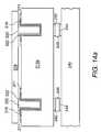
- FIG. 13is a sectional side view of an interface structure for a floating pin contact, such as may be present in a pin grid array (PGA) device
- FIG. 14is a top view of one of the pins of FIG. 13 .
- Coupling rigid pin connection structures to PC boardscan create mechanical stresses during fabrication and operation similar to those stresses created when bonding semiconductor chip pads to a substrate.
- Microprocessor chipscan create high temperatures which create large CTE differentials between the chips and PC boards on which they are attached.
- a substrate 210may comprise a PC board, a flexible interconnect layer, or any other structurally appropriate material.
- Low modulus interface dielectric regions 212may comprise materials similar to those discussed with respect to first interface dielectric layer 20 of FIG. 2 .
- the interface dielectric regions 212can be coated with metallization 214 which covers holes in the interface dielectric regions and has extensions 216 extending therefrom on each surface of substrate 210 .
- the metallizationis patterned to form extensions extending to a pad interconnect region 211 which is coupled by metallization runs to other pad interconnect regions or metallization areas (not shown) of the substrate.
- Solder 222can be applied between the metallization and an electrically conductive pin 220 that is attached to a support structure 218 .
- “Floating” through hole structuresresult because the interface dielectric regions and extensions permit the substrate to adjust to mechanical stresses to differing coefficients of thermal expansion and mechanical stresses encountered when inserting and removing pin grid arrays and other pin devices.
- the inventionis also useful in situations wherein the holes extend only part of the way through the interface dielectric material.
- FIG. 14 ais a sectional side view wherein holes do not extend all the way through an intermediate substrate 210 a.
- FIG. 14 aalso illustrates an embodiment wherein the entire substrate comprises a low modulus dielectric region.
- the substrate in FIG. 14 ais useful as a coupling board between a PC board 240 and a chip having pins, for example.
- Intermediate substrate 210 ahas intermediate pads 242 which can be coupled by internal metallization to pads or other metallization on an opposing surface (not shown) of the intermediate substrate and can be coupled by solder 246 to pads 244 of a PC board 240 , for example.
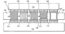
- FIG. 15is a sectional side view of a first surface represented by a printed circuit (PC) board 110 having first contact areas represented by array pads 112 which are coated with solder 114 and a second surface represented by a multichip module (MCM) 116 having second contact areas represented by array pads 118 which are coated with solder 120 and substantially aligned with respective array pads 112 .
- PCprinted circuit
- MCMmultichip module
- the present inventionis useful for coupling any of a number of metal areas.
- Other types of metal contact areas wherein the present invention can be usefulinclude, for example, metallization runs on substrates, metallized substrates, flexible interconnect structures, circuit chip pads, semiconductor wafer chip pads, infra red sensors, and holographic arrays.
- a surface such as PC board 110is a heat sink, includes a heat sink, or is attached to a heat sink 113 by an adhesive 111 (as shown in FIG. 15 ), the interface structures can create a thermal path that can be used to remove heat from an MCM.
- FIG. 16is a view similar to that of FIG. 15 further including several interface structures of the present invention.
- Each of the interface structureshas partially open interior to form a compliant joint between contact areas that it couples.
- Partially open interiormeans an interior that includes air (open spaces) or a compliant material in addition to the metal that is used to electrically couple the contact areas.
- crushed wire assembly 122which can be fabricated by pressing very fine metal wires into a structure having an appearance similar to that of steel wool and which intrinsically has spring action in several planes.
- wire assembly interface structuresare available from Cinch Connector Devices, of Elk Grove Village, IL, under the trademark name of FUZZ buttons. Wire paths are of lower inductance than BGA and CGA, so the size of power drivers for the electronics can be reduced.
- Wire assembly 122may comprise materials such as copper, gold, beryllium copper, gold-plated beryllium copper, and precious metal alloys such as palladium gold alloys. Typically the thickness of the wires range from about 0.5 mil to about 20 mils. A single compressed wire or a plurality of pressed wires can be used for a crushed wire assembly. For standard die pads which range from three to seven mils a diameter of wire assembly 122 would be about 3 mils. Wire assembly 122 can have any shape that permits coupling of two metal areas. For example, round, cylindrical, hour glass, and rectangular shapes are also appropriate for the wire assembly.
- a stranded core wire assembly 124which includes stranded vertical wires surrounded by insulation.
- the wirescomprise fine copper insulated wires.
- the insulationmust be a material that can withstand the temperatures at which soldering will occur.
- wirescan be bundled together with insulation and inserted between the two metal areas. If the wires are not exposed at the ends of the interface, a solvent dip, mechanical grinding, or etch process can be used to expose them. Because of the insulation, solder will not appreciably wick into the stranded core wire assemblies.
- Another interface structureis represented by a stranded core wire assembly 126 having removable insulation comprising a material such as a dissolvable polymer or a wire varnish.
- the use of sublimatable insulationis analogous to transformer insulating varnish which can be removed by sublimation or solvents, for example, after soldering is completed. As discussed below, when the insulation is removed from the vertical wires, an enhanced flexible structure is created.
- crushed wire assembly 128Another interface structure is represented by a crushed wire assembly 128 having capped ends 129 .
- Crushed wirecan have an uneven surface which can be evened out by caps comprising solder or a metal for facilitating soldering of the interface to the contact areas.
- Crushed wire assembliescan also include removable insulation or solder resist if desired to further inhibit solder wicking into crushed wires. Such solder wicking would reduce the flexibility of interfaces.
- Column 130comprises an outer layer of metallization 131 surrounding an inner area which may comprise a flexible material, one example of which is a polymer such as a rubber, or a hollow area.
- a flexible materialone example of which is a polymer such as a rubber, or a hollow area.
- materialcan be initially present during fabrication and later removed by a process such as sublimation or diffusion.
- one or more openingswould be needed in the outer layer of metallization to facilitate inner material removal.
- FIG. 17is a view similar to that of FIG. 16 further including an optional interposer structure 132 .
- the interposeris useful for holding the interface structures in position during soldering.
- the interposercan be either left in position after soldering or removed. If the interposer structure will be removed, a material such as wax or a polycarbonate which will dissolve or decompose in a solvent is useful. If the interposer structure will remain, any structurally appropriate material which can withstand the fabrication and operating temperatures of the assembly can be used. Examples include printed circuit boards and hard or hard filled plastics such as polyphenylene sulfide.
- FIG. 18is a schematic side view of interface structures 134 and interposer structure 132 .
- rivet-like shapes of the interface structuresare formed so that portions of the interface structures extend over the interposer structure to prevent the interface structures from falling out of the interposer structure.
- the rivet shapescan be formed in any conventional manner such as by pressing, for example.
- a loose fit rivet 134 awhich can move horizontally and/or vertically can be useful for reducing stress on the interposer structure and contact areas during high temperature operations, providing flexibility for solder to move interfaces in alignment with contact pads, and providing flexibility for curved surfaces.
- the interposer structureis dipped in a material that can be dissolved in a solvent, the interface structures are inserted in the interposer structure, the rivets are created, and the interposer structure is dipped in a solvent for removing the dipped material.
- the interface structurescan be modified by filling them with an insulative substance that prevents solder wicking into the crushed or vertically stranded wires. If the solder wicks deeply enough into the interfaces, a solid inflexible structure can result and would not provide effective CTE thermal stress accommodation.
- the insulative materialmay be added by a method such as dipping and comprise a polymer that can be dissolved in an appropriate solvent or any of a variety of organic and inorganic materials that can be removed by any of a number of techniques.
- a heat sublimation techniqueis described in Wojnarowski et al., U.S. Pat. No. 5,449,427, issued Sep. 12, 1995, for example.
- the insulative substanceis removed from the edges of the interface structures to be coupled prior to coupling.
- the insulative materialmay be removed, if desired, by any of a number of techniques such as sublimation, solvents, thermal decomposition, and the like to increase the spring-like compliance of the interface structures.
- FIG. 19is a view similar to that of FIG. 18 further including solderable surfaces 138 on the interface.
- the top and bottom areas of the interfacescan be chemically treated or mechanically ground to reveal a solderable interface.
- Plasmas, RIE (reactive ion etching), solvents, flame treatments, or mechanical grinding, for example,can be used to expose desired areas of the rivet buttons.
- An optional step of pre-tinning an interface structure surface by dipping it in solder or metallizing it by electroless metallizationcan facilitate soldering of the interface surface to the contact area and help the surface tension of the solder to move the interfaces into alignment with the contact pads.
- Repaircan be accomplished by heating the interfaces and melting the solder. If no insulating material is present (either there never was any or any such material was removed), the solder wicks away from the solder joint and into the interface structures and thus the excess solder is removed from the repair area without requiring rework by hand.
- FIG. 20is a view similar to that of FIG. 17 showing a curved base 310 with pads 312 coupled to pads 318 of surface 316 by interfaces 334 loosely fit into an interposer 332 .
Landscapes
- Engineering & Computer Science (AREA)
- Microelectronics & Electronic Packaging (AREA)
- Computer Hardware Design (AREA)
- Power Engineering (AREA)
- Physics & Mathematics (AREA)
- Condensed Matter Physics & Semiconductors (AREA)
- General Physics & Mathematics (AREA)
- Manufacturing & Machinery (AREA)
- Ceramic Engineering (AREA)
- Production Of Multi-Layered Print Wiring Board (AREA)
- Structures For Mounting Electric Components On Printed Circuit Boards (AREA)
Abstract
Description
Claims (14)
Priority Applications (1)
| Application Number | Priority Date | Filing Date | Title |
|---|---|---|---|
| US09/459,586US6298551B1 (en) | 1996-12-23 | 1999-12-13 | Methods of forming compliant interface structures with partially open interiors for coupling two electrically conductive contact areas |
Applications Claiming Priority (3)
| Application Number | Priority Date | Filing Date | Title |
|---|---|---|---|
| US08/781,972US5900674A (en) | 1996-12-23 | 1996-12-23 | Interface structures for electronic devices |
| US09/139,049US6046410A (en) | 1996-12-23 | 1998-08-24 | Interface structures for electronic devices |
| US09/459,586US6298551B1 (en) | 1996-12-23 | 1999-12-13 | Methods of forming compliant interface structures with partially open interiors for coupling two electrically conductive contact areas |
Related Parent Applications (1)
| Application Number | Title | Priority Date | Filing Date |
|---|---|---|---|
| US09/139,049DivisionUS6046410A (en) | 1996-12-23 | 1998-08-24 | Interface structures for electronic devices |
Publications (1)
| Publication Number | Publication Date |
|---|---|
| US6298551B1true US6298551B1 (en) | 2001-10-09 |
Family
ID=25124523
Family Applications (3)
| Application Number | Title | Priority Date | Filing Date |
|---|---|---|---|
| US08/781,972Expired - LifetimeUS5900674A (en) | 1996-12-23 | 1996-12-23 | Interface structures for electronic devices |
| US09/139,049Expired - LifetimeUS6046410A (en) | 1996-12-23 | 1998-08-24 | Interface structures for electronic devices |
| US09/459,586Expired - LifetimeUS6298551B1 (en) | 1996-12-23 | 1999-12-13 | Methods of forming compliant interface structures with partially open interiors for coupling two electrically conductive contact areas |
Family Applications Before (2)
| Application Number | Title | Priority Date | Filing Date |
|---|---|---|---|
| US08/781,972Expired - LifetimeUS5900674A (en) | 1996-12-23 | 1996-12-23 | Interface structures for electronic devices |
| US09/139,049Expired - LifetimeUS6046410A (en) | 1996-12-23 | 1998-08-24 | Interface structures for electronic devices |
Country Status (1)
| Country | Link |
|---|---|
| US (3) | US5900674A (en) |
Cited By (64)
| Publication number | Priority date | Publication date | Assignee | Title |
|---|---|---|---|---|
| US6559388B1 (en)* | 1999-06-08 | 2003-05-06 | International Business Machines Corporation | Strain relief for substrates having a low coefficient of thermal expansion |
| US6636543B2 (en)* | 2001-06-26 | 2003-10-21 | The Furukawa Electric Co., Ltd. | Semiconductor device and surface emitting semiconductor laser device |
| US20030218246A1 (en)* | 2002-05-22 | 2003-11-27 | Hirofumi Abe | Semiconductor device passing large electric current |
| US20040192080A1 (en)* | 2003-03-24 | 2004-09-30 | Che-Yu Li | Electrical contact |
| US20050151273A1 (en)* | 2003-12-30 | 2005-07-14 | Arnold Richard W. | Semiconductor chip package |
| US20050242425A1 (en)* | 2004-04-30 | 2005-11-03 | Leal George R | Semiconductor device with a protected active die region and method therefor |
| US20060278999A1 (en)* | 2003-09-29 | 2006-12-14 | Phoenix Precision Technology Corporation | Substrate for Pre-Soldering Material and Fabrication Method Thereof |
| US7217999B1 (en)* | 1999-10-05 | 2007-05-15 | Nec Electronics Corporation | Multilayer interconnection board, semiconductor device having the same, and method of forming the same as well as method of mounting the semiconductor chip on the interconnection board |
| US20090188705A1 (en)* | 2008-01-26 | 2009-07-30 | International Business Machines Corporation | Construction of Reliable Stacked Via in Electronic Substrates - Vertical Stiffness Control Method |
| US20100263923A1 (en)* | 2009-04-16 | 2010-10-21 | Shinko Electric Industries Co., Ltd. | Wiring substrate having columnar protruding part |
| USD648642S1 (en) | 2009-10-21 | 2011-11-15 | Lennox Industries Inc. | Thin cover plate for an electronic system controller |
| USD648641S1 (en) | 2009-10-21 | 2011-11-15 | Lennox Industries Inc. | Thin cover plate for an electronic system controller |
| US8239066B2 (en) | 2008-10-27 | 2012-08-07 | Lennox Industries Inc. | System and method of use for a user interface dashboard of a heating, ventilation and air conditioning network |
| US8255086B2 (en) | 2008-10-27 | 2012-08-28 | Lennox Industries Inc. | System recovery in a heating, ventilation and air conditioning network |
| US8260444B2 (en) | 2010-02-17 | 2012-09-04 | Lennox Industries Inc. | Auxiliary controller of a HVAC system |
| US8295981B2 (en) | 2008-10-27 | 2012-10-23 | Lennox Industries Inc. | Device commissioning in a heating, ventilation and air conditioning network |
| US8352081B2 (en) | 2008-10-27 | 2013-01-08 | Lennox Industries Inc. | Communication protocol system and method for a distributed-architecture heating, ventilation and air conditioning network |
| US8352080B2 (en) | 2008-10-27 | 2013-01-08 | Lennox Industries Inc. | Communication protocol system and method for a distributed-architecture heating, ventilation and air conditioning network |
| US8433446B2 (en) | 2008-10-27 | 2013-04-30 | Lennox Industries, Inc. | Alarm and diagnostics system and method for a distributed-architecture heating, ventilation and air conditioning network |
| US8437878B2 (en) | 2008-10-27 | 2013-05-07 | Lennox Industries Inc. | Alarm and diagnostics system and method for a distributed architecture heating, ventilation and air conditioning network |
| US8437877B2 (en) | 2008-10-27 | 2013-05-07 | Lennox Industries Inc. | System recovery in a heating, ventilation and air conditioning network |
| US8442693B2 (en) | 2008-10-27 | 2013-05-14 | Lennox Industries, Inc. | System and method of use for a user interface dashboard of a heating, ventilation and air conditioning network |
| US8452906B2 (en) | 2008-10-27 | 2013-05-28 | Lennox Industries, Inc. | Communication protocol system and method for a distributed-architecture heating, ventilation and air conditioning network |
| US8452456B2 (en) | 2008-10-27 | 2013-05-28 | Lennox Industries Inc. | System and method of use for a user interface dashboard of a heating, ventilation and air conditioning network |
| US8463443B2 (en) | 2008-10-27 | 2013-06-11 | Lennox Industries, Inc. | Memory recovery scheme and data structure in a heating, ventilation and air conditioning network |
| US8463442B2 (en) | 2008-10-27 | 2013-06-11 | Lennox Industries, Inc. | Alarm and diagnostics system and method for a distributed architecture heating, ventilation and air conditioning network |
| US8543243B2 (en) | 2008-10-27 | 2013-09-24 | Lennox Industries, Inc. | System and method of use for a user interface dashboard of a heating, ventilation and air conditioning network |
| US8548630B2 (en) | 2008-10-27 | 2013-10-01 | Lennox Industries, Inc. | Alarm and diagnostics system and method for a distributed-architecture heating, ventilation and air conditioning network |
| US8560125B2 (en) | 2008-10-27 | 2013-10-15 | Lennox Industries | Communication protocol system and method for a distributed-architecture heating, ventilation and air conditioning network |
| US8564400B2 (en) | 2008-10-27 | 2013-10-22 | Lennox Industries, Inc. | Communication protocol system and method for a distributed-architecture heating, ventilation and air conditioning network |
| US8600559B2 (en) | 2008-10-27 | 2013-12-03 | Lennox Industries Inc. | Method of controlling equipment in a heating, ventilation and air conditioning network |
| US8600558B2 (en) | 2008-10-27 | 2013-12-03 | Lennox Industries Inc. | System recovery in a heating, ventilation and air conditioning network |
| US8615326B2 (en) | 2008-10-27 | 2013-12-24 | Lennox Industries Inc. | System and method of use for a user interface dashboard of a heating, ventilation and air conditioning network |
| US8655490B2 (en) | 2008-10-27 | 2014-02-18 | Lennox Industries, Inc. | System and method of use for a user interface dashboard of a heating, ventilation and air conditioning network |
| US8655491B2 (en) | 2008-10-27 | 2014-02-18 | Lennox Industries Inc. | Alarm and diagnostics system and method for a distributed architecture heating, ventilation and air conditioning network |
| US8661165B2 (en) | 2008-10-27 | 2014-02-25 | Lennox Industries, Inc. | Device abstraction system and method for a distributed architecture heating, ventilation and air conditioning system |
| US8674506B2 (en)* | 2009-12-17 | 2014-03-18 | International Business Machines Corporation | Structures and methods to reduce maximum current density in a solder ball |
| US8694164B2 (en) | 2008-10-27 | 2014-04-08 | Lennox Industries, Inc. | Interactive user guidance interface for a heating, ventilation and air conditioning system |
| US8725298B2 (en) | 2008-10-27 | 2014-05-13 | Lennox Industries, Inc. | Alarm and diagnostics system and method for a distributed architecture heating, ventilation and conditioning network |
| US8744629B2 (en) | 2008-10-27 | 2014-06-03 | Lennox Industries Inc. | System and method of use for a user interface dashboard of a heating, ventilation and air conditioning network |
| US8762666B2 (en) | 2008-10-27 | 2014-06-24 | Lennox Industries, Inc. | Backup and restoration of operation control data in a heating, ventilation and air conditioning network |
| US8774210B2 (en) | 2008-10-27 | 2014-07-08 | Lennox Industries, Inc. | Communication protocol system and method for a distributed-architecture heating, ventilation and air conditioning network |
| US8778792B2 (en) | 2010-12-08 | 2014-07-15 | International Business Machines Corporation | Solder bump connections |
| US8788100B2 (en) | 2008-10-27 | 2014-07-22 | Lennox Industries Inc. | System and method for zoning a distributed-architecture heating, ventilation and air conditioning network |
| US8798796B2 (en) | 2008-10-27 | 2014-08-05 | Lennox Industries Inc. | General control techniques in a heating, ventilation and air conditioning network |
| US8802981B2 (en) | 2008-10-27 | 2014-08-12 | Lennox Industries Inc. | Flush wall mount thermostat and in-set mounting plate for a heating, ventilation and air conditioning system |
| US8855825B2 (en) | 2008-10-27 | 2014-10-07 | Lennox Industries Inc. | Device abstraction system and method for a distributed-architecture heating, ventilation and air conditioning system |
| US8874815B2 (en) | 2008-10-27 | 2014-10-28 | Lennox Industries, Inc. | Communication protocol system and method for a distributed architecture heating, ventilation and air conditioning network |
| US8892797B2 (en) | 2008-10-27 | 2014-11-18 | Lennox Industries Inc. | Communication protocol system and method for a distributed-architecture heating, ventilation and air conditioning network |
| US8977794B2 (en) | 2008-10-27 | 2015-03-10 | Lennox Industries, Inc. | Communication protocol system and method for a distributed-architecture heating, ventilation and air conditioning network |
| US8994539B2 (en) | 2008-10-27 | 2015-03-31 | Lennox Industries, Inc. | Alarm and diagnostics system and method for a distributed-architecture heating, ventilation and air conditioning network |
| US9152155B2 (en) | 2008-10-27 | 2015-10-06 | Lennox Industries Inc. | Device abstraction system and method for a distributed-architecture heating, ventilation and air conditioning system |
| US9214385B2 (en) | 2009-12-17 | 2015-12-15 | Globalfoundries Inc. | Semiconductor device including passivation layer encapsulant |
| US9261888B2 (en) | 2008-10-27 | 2016-02-16 | Lennox Industries Inc. | System and method of use for a user interface dashboard of a heating, ventilation and air conditioning network |
| US9268345B2 (en) | 2008-10-27 | 2016-02-23 | Lennox Industries Inc. | System and method of use for a user interface dashboard of a heating, ventilation and air conditioning network |
| US9325517B2 (en) | 2008-10-27 | 2016-04-26 | Lennox Industries Inc. | Device abstraction system and method for a distributed-architecture heating, ventilation and air conditioning system |
| US9377768B2 (en) | 2008-10-27 | 2016-06-28 | Lennox Industries Inc. | Memory recovery scheme and data structure in a heating, ventilation and air conditioning network |
| US9432208B2 (en) | 2008-10-27 | 2016-08-30 | Lennox Industries Inc. | Device abstraction system and method for a distributed architecture heating, ventilation and air conditioning system |
| US9632490B2 (en) | 2008-10-27 | 2017-04-25 | Lennox Industries Inc. | System and method for zoning a distributed architecture heating, ventilation and air conditioning network |
| US9651925B2 (en) | 2008-10-27 | 2017-05-16 | Lennox Industries Inc. | System and method for zoning a distributed-architecture heating, ventilation and air conditioning network |
| US9678486B2 (en) | 2008-10-27 | 2017-06-13 | Lennox Industries Inc. | Device abstraction system and method for a distributed-architecture heating, ventilation and air conditioning system |
| US10064275B1 (en)* | 2017-07-18 | 2018-08-28 | Mellanox Technologies, Ltd. | Extending the lifetime of a leadless SMT solder joint using pads comprising spring-shaped traces |
| US10779403B2 (en) | 2018-09-20 | 2020-09-15 | Apple Inc. | Shorting pattern between pads of a camera module |
| US11559442B2 (en) | 2017-12-28 | 2023-01-24 | Stryker Corporation | Patient transport apparatus with controlled auxiliary wheel deployment |
Families Citing this family (68)
| Publication number | Priority date | Publication date | Assignee | Title |
|---|---|---|---|---|
| US6146535A (en)* | 1994-06-24 | 2000-11-14 | Sutherland; George | Organic recovery method using hollow fiber microfilters |
| US6528736B1 (en)* | 1997-01-21 | 2003-03-04 | Visteon Global Technologies, Inc. | Multi-layer printed circuit board and method of making same |
| JP3335575B2 (en)* | 1997-06-06 | 2002-10-21 | 松下電器産業株式会社 | Semiconductor device and manufacturing method thereof |
| KR100272737B1 (en)* | 1998-01-09 | 2001-01-15 | 윤종용 | reel printed circuit board and chip on board packages using the reel printed circuit board |
| US6914196B2 (en) | 1998-01-09 | 2005-07-05 | Samsung Electronics Co., Ltd. | Reel-deployed printed circuit board |
| US6198168B1 (en)* | 1998-01-20 | 2001-03-06 | Micron Technologies, Inc. | Integrated circuits using high aspect ratio vias through a semiconductor wafer and method for forming same |
| US6624505B2 (en) | 1998-02-06 | 2003-09-23 | Shellcase, Ltd. | Packaged integrated circuits and methods of producing thereof |
| IL123207A0 (en) | 1998-02-06 | 1998-09-24 | Shellcase Ltd | Integrated circuit device |
| US6150188A (en) | 1998-02-26 | 2000-11-21 | Micron Technology Inc. | Integrated circuits using optical fiber interconnects formed through a semiconductor wafer and methods for forming same |
| US6090636A (en)* | 1998-02-26 | 2000-07-18 | Micron Technology, Inc. | Integrated circuits using optical waveguide interconnects formed through a semiconductor wafer and methods for forming same |
| US6115262A (en)* | 1998-06-08 | 2000-09-05 | Ford Motor Company | Enhanced mounting pads for printed circuit boards |
| JPH11354680A (en)* | 1998-06-11 | 1999-12-24 | Sony Corp | Printed wiring board and semiconductor package using the same |
| SG82591A1 (en)* | 1998-12-17 | 2001-08-21 | Eriston Technologies Pte Ltd | Bumpless flip chip assembly with solder via |
| US6980017B1 (en) | 1999-03-10 | 2005-12-27 | Micron Technology, Inc. | Test interconnect for bumped semiconductor components and method of fabrication |
| US6437591B1 (en) | 1999-03-25 | 2002-08-20 | Micron Technology, Inc. | Test interconnect for bumped semiconductor components and method of fabrication |
| US6400570B2 (en)* | 1999-09-10 | 2002-06-04 | Lockheed Martin Corporation | Plated through-holes for signal interconnections in an electronic component assembly |
| US6769921B1 (en)* | 1999-10-15 | 2004-08-03 | Dell Usa L.P. | Printed circuit board electromagnetic energy device |
| US6507113B1 (en) | 1999-11-19 | 2003-01-14 | General Electric Company | Electronic interface structures and methods of fabrication |
| JP2001244391A (en)* | 1999-12-21 | 2001-09-07 | Toyota Central Res & Dev Lab Inc | Multi-chip module cooling structure |
| US6560108B2 (en)* | 2000-02-16 | 2003-05-06 | Hughes Electronics Corporation | Chip scale packaging on CTE matched printed wiring boards |
| US6399896B1 (en)* | 2000-03-15 | 2002-06-04 | International Business Machines Corporation | Circuit package having low modulus, conformal mounting pads |
| US6423905B1 (en) | 2000-05-01 | 2002-07-23 | International Business Machines Corporation | Printed wiring board with improved plated through hole fatigue life |
| US6506979B1 (en)* | 2000-05-12 | 2003-01-14 | Shipley Company, L.L.C. | Sequential build circuit board |
| KR100855015B1 (en)* | 2000-12-21 | 2008-08-28 | 테쎄라 테크놀로지스 헝가리 케이에프티. | Packaged integrated circuit and manufacturing method thereof |
| US6979202B2 (en) | 2001-01-12 | 2005-12-27 | Litton Systems, Inc. | High-speed electrical connector |
| US6910897B2 (en) | 2001-01-12 | 2005-06-28 | Litton Systems, Inc. | Interconnection system |
| US6843657B2 (en) | 2001-01-12 | 2005-01-18 | Litton Systems Inc. | High speed, high density interconnect system for differential and single-ended transmission applications |
| US6856007B2 (en) | 2001-08-28 | 2005-02-15 | Tessera, Inc. | High-frequency chip packages |
| US7275562B2 (en)* | 2001-10-17 | 2007-10-02 | Agilent Technologies, Inc. | Extensible spiral for flex circuit |
| JP2003224087A (en)* | 2002-01-28 | 2003-08-08 | Disco Abrasive Syst Ltd | Processing method of semiconductor wafer |
| US7098072B2 (en)* | 2002-03-01 | 2006-08-29 | Agng, Llc | Fluxless assembly of chip size semiconductor packages |
| RU2262153C2 (en)* | 2002-03-01 | 2005-10-10 | ЭйДжиЭнДжи, ЛЛСи. | Flux-free assembly of chip-sized semiconductor parts |
| WO2003075337A1 (en)* | 2002-03-01 | 2003-09-12 | Agng, Llc | Fluxless assembly of chip size semiconductor packages |
| US6935792B2 (en)* | 2002-10-21 | 2005-08-30 | General Electric Company | Optoelectronic package and fabrication method |
| US7033664B2 (en) | 2002-10-22 | 2006-04-25 | Tessera Technologies Hungary Kft | Methods for producing packaged integrated circuit devices and packaged integrated circuit devices produced thereby |
| DE60329857D1 (en)* | 2002-10-24 | 2009-12-10 | Ibm | MANUFACTURE OF A LAND OF GRID ARRAY USING ELASTOMERKERN AND LEADING METAL SHEET OR GRILLE |
| US20040132320A1 (en)* | 2002-12-20 | 2004-07-08 | Dittmann Larry E. | Land grid array connector |
| US6972480B2 (en) | 2003-06-16 | 2005-12-06 | Shellcase Ltd. | Methods and apparatus for packaging integrated circuit devices |
| US6908025B2 (en)* | 2003-06-26 | 2005-06-21 | Internatioanl Business Machines Corporation | Preparing MCM hat for removal |
| CN100587962C (en) | 2003-07-03 | 2010-02-03 | 泰塞拉技术匈牙利公司 | Method and apparatus for packaging integrated circuit devices |
| TWI234258B (en)* | 2003-08-01 | 2005-06-11 | Advanced Semiconductor Eng | Substrate with reinforced structure of contact pad |
| WO2005031861A1 (en)* | 2003-09-26 | 2005-04-07 | Tessera, Inc. | Structure and method of making capped chips including a flowable conductive medium |
| US20050067681A1 (en)* | 2003-09-26 | 2005-03-31 | Tessera, Inc. | Package having integral lens and wafer-scale fabrication method therefor |
| US7294919B2 (en)* | 2003-11-26 | 2007-11-13 | Avago Technologies General Ip (Singapore) Pte. Ltd. | Device having a complaint element pressed between substrates |
| US20050139984A1 (en)* | 2003-12-19 | 2005-06-30 | Tessera, Inc. | Package element and packaged chip having severable electrically conductive ties |
| US20050189635A1 (en)* | 2004-03-01 | 2005-09-01 | Tessera, Inc. | Packaged acoustic and electromagnetic transducer chips |
| US7112877B2 (en)* | 2004-06-28 | 2006-09-26 | General Electric Company | High density package with wrap around interconnect |
| DE102004040414B4 (en)* | 2004-08-19 | 2006-08-31 | Infineon Technologies Ag | A method of manufacturing a wiring substrate of a semiconductor device having external contact pads for external contacts |
| DE102005002987A1 (en)* | 2005-01-21 | 2006-07-27 | Siemens Ag | Track structure to minimize thermomechanical loads |
| US8143095B2 (en) | 2005-03-22 | 2012-03-27 | Tessera, Inc. | Sequential fabrication of vertical conductive interconnects in capped chips |
| US7566853B2 (en)* | 2005-08-12 | 2009-07-28 | Tessera, Inc. | Image sensor employing a plurality of photodetector arrays and/or rear-illuminated architecture |
| US20070117268A1 (en)* | 2005-11-23 | 2007-05-24 | Baker Hughes, Inc. | Ball grid attachment |
| US20070190747A1 (en)* | 2006-01-23 | 2007-08-16 | Tessera Technologies Hungary Kft. | Wafer level packaging to lidded chips |
| US7936062B2 (en) | 2006-01-23 | 2011-05-03 | Tessera Technologies Ireland Limited | Wafer level chip packaging |
| US20080002460A1 (en)* | 2006-03-01 | 2008-01-03 | Tessera, Inc. | Structure and method of making lidded chips |
| US7271485B1 (en) | 2006-09-11 | 2007-09-18 | Agere Systems Inc. | Systems and methods for distributing I/O in a semiconductor device |
| US7616451B2 (en)* | 2006-10-13 | 2009-11-10 | Stmicroelectronics S.R.L. | Semiconductor package substrate and method, in particular for MEMS devices |
| US8604605B2 (en) | 2007-01-05 | 2013-12-10 | Invensas Corp. | Microelectronic assembly with multi-layer support structure |
| JP5269563B2 (en) | 2008-11-28 | 2013-08-21 | 新光電気工業株式会社 | Wiring board and manufacturing method thereof |
| JP5649788B2 (en)* | 2009-01-21 | 2015-01-07 | 富士通株式会社 | Printed circuit board, printed circuit board mounting structure, and printed circuit board mounting method |
| US8927872B2 (en) | 2009-02-20 | 2015-01-06 | Telefonaktiebolaget L M Ericsson (Publ) | Thermal pad and method of forming the same |
| US8344495B2 (en)* | 2009-12-11 | 2013-01-01 | Stats Chippac Ltd. | Integrated circuit packaging system with interconnect and method of manufacture thereof |
| TWI495074B (en)* | 2012-11-30 | 2015-08-01 | Ind Tech Res Inst | Stress relief structure |
| US10134696B2 (en)* | 2014-12-19 | 2018-11-20 | Myron Walker | Spoked solder pad to improve solderability and self-alignment of integrated circuit packages |
| CN107113963B (en)* | 2014-12-19 | 2020-07-24 | 麦伦·沃克 | Spoke pads for improved self-alignment and solderability of integrated circuit packages |
| USD816135S1 (en) | 2014-12-19 | 2018-04-24 | Myron Walker | Spoked solder pad |
| US9801269B1 (en) | 2016-05-10 | 2017-10-24 | Northrop Grumman Systems Corporation | Resilient miniature integrated electrical connector |
| EP4056528B1 (en) | 2021-03-11 | 2025-08-27 | Murata Manufacturing Co., Ltd. | Method for bonding wafers, and a wafer |
Citations (25)
| Publication number | Priority date | Publication date | Assignee | Title |
|---|---|---|---|---|
| DE3129568A1 (en) | 1980-07-28 | 1982-04-22 | Hitachi, Ltd., Tokyo | Connection system of a semiconductor arrangement and method for manufacturing it |
| US4628406A (en) | 1985-05-20 | 1986-12-09 | Tektronix, Inc. | Method of packaging integrated circuit chips, and integrated circuit package |
| US4641222A (en) | 1984-05-29 | 1987-02-03 | Motorola, Inc. | Mounting system for stress relief in surface mounted components |
| US4642889A (en)* | 1985-04-29 | 1987-02-17 | Amp Incorporated | Compliant interconnection and method therefor |
| US4689262A (en)* | 1984-05-21 | 1987-08-25 | Cts Corporation | Electrically insulating substrate |
| EP0277606A2 (en) | 1987-02-02 | 1988-08-10 | International Business Machines Corporation | Full panel electronic packaging structure |
| US4835704A (en) | 1986-12-29 | 1989-05-30 | General Electric Company | Adaptive lithography system to provide high density interconnect |
| US4845542A (en) | 1987-03-19 | 1989-07-04 | Unisys Corporation | Interconnect for layered integrated circuit assembly |
| US4847146A (en) | 1988-03-21 | 1989-07-11 | Hughes Aircraft Company | Process for fabricating compliant layer board with selectively isolated solder pads |
| US4874721A (en) | 1985-11-11 | 1989-10-17 | Nec Corporation | Method of manufacturing a multichip package with increased adhesive strength |
| US4894115A (en) | 1989-02-14 | 1990-01-16 | General Electric Company | Laser beam scanning method for forming via holes in polymer materials |
| US4954878A (en)* | 1989-06-29 | 1990-09-04 | Digital Equipment Corp. | Method of packaging and powering integrated circuit chips and the chip assembly formed thereby |
| US5161093A (en) | 1990-07-02 | 1992-11-03 | General Electric Company | Multiple lamination high density interconnect process and structure employing a variable crosslinking adhesive |
| US5352926A (en) | 1993-01-04 | 1994-10-04 | Motorola, Inc. | Flip chip package and method of making |
| US5440075A (en)* | 1992-09-22 | 1995-08-08 | Matsushita Electric Industrial Co., Ltd. | Two-sided printed circuit board a multi-layered printed circuit board |
| US5449427A (en) | 1994-05-23 | 1995-09-12 | General Electric Company | Processing low dielectric constant materials for high speed electronics |
| US5454904A (en) | 1993-01-04 | 1995-10-03 | General Electric Company | Micromachining methods for making micromechanical moving structures including multiple contact switching system |
| US5473119A (en) | 1993-02-05 | 1995-12-05 | W. L. Gore & Associates, Inc. | Stress-resistant circuit board |
| US5474458A (en)* | 1993-07-13 | 1995-12-12 | Fujitsu Limited | Interconnect carriers having high-density vertical connectors and methods for making the same |
| US5502002A (en) | 1992-05-21 | 1996-03-26 | Hughes Aircraft Company | Polyimide passivation of GaAs microwave monolithic integrated circuit flip-chip |
| US5527741A (en) | 1994-10-11 | 1996-06-18 | Martin Marietta Corporation | Fabrication and structures of circuit modules with flexible interconnect layers |
| US5731073A (en) | 1996-10-01 | 1998-03-24 | W. L. Gore & Associates, Inc. | Reusable, selectively conductive, Z-axis, elastomeric composite substrate |
| US5759047A (en)* | 1996-05-24 | 1998-06-02 | International Business Machines Corporation | Flexible circuitized interposer with apertured member and method for making same |
| US5806181A (en)* | 1993-11-16 | 1998-09-15 | Formfactor, Inc. | Contact carriers (tiles) for populating larger substrates with spring contacts |
| US6020220A (en)* | 1996-07-09 | 2000-02-01 | Tessera, Inc. | Compliant semiconductor chip assemblies and methods of making same |
- 1996
- 1996-12-23USUS08/781,972patent/US5900674A/ennot_activeExpired - Lifetime
- 1998
- 1998-08-24USUS09/139,049patent/US6046410A/ennot_activeExpired - Lifetime
- 1999
- 1999-12-13USUS09/459,586patent/US6298551B1/ennot_activeExpired - Lifetime
Patent Citations (26)
| Publication number | Priority date | Publication date | Assignee | Title |
|---|---|---|---|---|
| DE3129568A1 (en) | 1980-07-28 | 1982-04-22 | Hitachi, Ltd., Tokyo | Connection system of a semiconductor arrangement and method for manufacturing it |
| US4689262A (en)* | 1984-05-21 | 1987-08-25 | Cts Corporation | Electrically insulating substrate |
| US4641222A (en) | 1984-05-29 | 1987-02-03 | Motorola, Inc. | Mounting system for stress relief in surface mounted components |
| US4642889A (en)* | 1985-04-29 | 1987-02-17 | Amp Incorporated | Compliant interconnection and method therefor |
| US4628406A (en) | 1985-05-20 | 1986-12-09 | Tektronix, Inc. | Method of packaging integrated circuit chips, and integrated circuit package |
| US4874721A (en) | 1985-11-11 | 1989-10-17 | Nec Corporation | Method of manufacturing a multichip package with increased adhesive strength |
| US4835704A (en) | 1986-12-29 | 1989-05-30 | General Electric Company | Adaptive lithography system to provide high density interconnect |
| EP0277606A2 (en) | 1987-02-02 | 1988-08-10 | International Business Machines Corporation | Full panel electronic packaging structure |
| US4845542A (en) | 1987-03-19 | 1989-07-04 | Unisys Corporation | Interconnect for layered integrated circuit assembly |
| US4847146A (en) | 1988-03-21 | 1989-07-11 | Hughes Aircraft Company | Process for fabricating compliant layer board with selectively isolated solder pads |
| US4894115A (en) | 1989-02-14 | 1990-01-16 | General Electric Company | Laser beam scanning method for forming via holes in polymer materials |
| EP0407103A2 (en) | 1989-06-29 | 1991-01-09 | Digital Equipment Corporation | Method of packaging and powering integrated circuit chips and the chip assembly formed thereby |
| US4954878A (en)* | 1989-06-29 | 1990-09-04 | Digital Equipment Corp. | Method of packaging and powering integrated circuit chips and the chip assembly formed thereby |
| US5161093A (en) | 1990-07-02 | 1992-11-03 | General Electric Company | Multiple lamination high density interconnect process and structure employing a variable crosslinking adhesive |
| US5502002A (en) | 1992-05-21 | 1996-03-26 | Hughes Aircraft Company | Polyimide passivation of GaAs microwave monolithic integrated circuit flip-chip |
| US5440075A (en)* | 1992-09-22 | 1995-08-08 | Matsushita Electric Industrial Co., Ltd. | Two-sided printed circuit board a multi-layered printed circuit board |
| US5352926A (en) | 1993-01-04 | 1994-10-04 | Motorola, Inc. | Flip chip package and method of making |
| US5454904A (en) | 1993-01-04 | 1995-10-03 | General Electric Company | Micromachining methods for making micromechanical moving structures including multiple contact switching system |
| US5473119A (en) | 1993-02-05 | 1995-12-05 | W. L. Gore & Associates, Inc. | Stress-resistant circuit board |
| US5474458A (en)* | 1993-07-13 | 1995-12-12 | Fujitsu Limited | Interconnect carriers having high-density vertical connectors and methods for making the same |
| US5806181A (en)* | 1993-11-16 | 1998-09-15 | Formfactor, Inc. | Contact carriers (tiles) for populating larger substrates with spring contacts |
| US5449427A (en) | 1994-05-23 | 1995-09-12 | General Electric Company | Processing low dielectric constant materials for high speed electronics |
| US5527741A (en) | 1994-10-11 | 1996-06-18 | Martin Marietta Corporation | Fabrication and structures of circuit modules with flexible interconnect layers |
| US5759047A (en)* | 1996-05-24 | 1998-06-02 | International Business Machines Corporation | Flexible circuitized interposer with apertured member and method for making same |
| US6020220A (en)* | 1996-07-09 | 2000-02-01 | Tessera, Inc. | Compliant semiconductor chip assemblies and methods of making same |
| US5731073A (en) | 1996-10-01 | 1998-03-24 | W. L. Gore & Associates, Inc. | Reusable, selectively conductive, Z-axis, elastomeric composite substrate |
Cited By (79)
| Publication number | Priority date | Publication date | Assignee | Title |
|---|---|---|---|---|
| US6559388B1 (en)* | 1999-06-08 | 2003-05-06 | International Business Machines Corporation | Strain relief for substrates having a low coefficient of thermal expansion |
| US8008130B2 (en) | 1999-10-05 | 2011-08-30 | Renesas Electronics Corporation | Multilayer interconnection board, semiconductor device having the same, and method of forming the same as well as method of mounting the semicondutor chip on the interconnection board |
| US7217999B1 (en)* | 1999-10-05 | 2007-05-15 | Nec Electronics Corporation | Multilayer interconnection board, semiconductor device having the same, and method of forming the same as well as method of mounting the semiconductor chip on the interconnection board |
| US6636543B2 (en)* | 2001-06-26 | 2003-10-21 | The Furukawa Electric Co., Ltd. | Semiconductor device and surface emitting semiconductor laser device |
| US20030218246A1 (en)* | 2002-05-22 | 2003-11-27 | Hirofumi Abe | Semiconductor device passing large electric current |
| US20040192080A1 (en)* | 2003-03-24 | 2004-09-30 | Che-Yu Li | Electrical contact |
| US7040902B2 (en) | 2003-03-24 | 2006-05-09 | Che-Yu Li & Company, Llc | Electrical contact |
| US7319276B2 (en)* | 2003-09-29 | 2008-01-15 | Phoenix Precision Technology Corporation | Substrate for pre-soldering material and fabrication method thereof |
| US20060278999A1 (en)* | 2003-09-29 | 2006-12-14 | Phoenix Precision Technology Corporation | Substrate for Pre-Soldering Material and Fabrication Method Thereof |
| US20050151273A1 (en)* | 2003-12-30 | 2005-07-14 | Arnold Richard W. | Semiconductor chip package |
| US20050242425A1 (en)* | 2004-04-30 | 2005-11-03 | Leal George R | Semiconductor device with a protected active die region and method therefor |
| US20090188705A1 (en)* | 2008-01-26 | 2009-07-30 | International Business Machines Corporation | Construction of Reliable Stacked Via in Electronic Substrates - Vertical Stiffness Control Method |
| WO2009092677A3 (en)* | 2008-01-26 | 2009-10-29 | International Business Machines Corporation | Construction of reliable stacked via in electronic substrates - vertical stiffness control method |
| US9099458B2 (en)* | 2008-01-26 | 2015-08-04 | International Business Machines Corporation | Construction of reliable stacked via in electronic substrates—vertical stiffness control method |
| US8258410B2 (en) | 2008-01-26 | 2012-09-04 | International Business Machines Corporation | Construction of reliable stacked via in electronic substrates—vertical stiffness control method |
| US20120267158A1 (en)* | 2008-01-26 | 2012-10-25 | International Business Machines Corporation | Construction of reliable stacked via in electronic substrates - vertical stiffness control method |
| US8600558B2 (en) | 2008-10-27 | 2013-12-03 | Lennox Industries Inc. | System recovery in a heating, ventilation and air conditioning network |
| US8761945B2 (en) | 2008-10-27 | 2014-06-24 | Lennox Industries Inc. | Device commissioning in a heating, ventilation and air conditioning network |
| US8239066B2 (en) | 2008-10-27 | 2012-08-07 | Lennox Industries Inc. | System and method of use for a user interface dashboard of a heating, ventilation and air conditioning network |
| US9678486B2 (en) | 2008-10-27 | 2017-06-13 | Lennox Industries Inc. | Device abstraction system and method for a distributed-architecture heating, ventilation and air conditioning system |
| US8295981B2 (en) | 2008-10-27 | 2012-10-23 | Lennox Industries Inc. | Device commissioning in a heating, ventilation and air conditioning network |
| US9651925B2 (en) | 2008-10-27 | 2017-05-16 | Lennox Industries Inc. | System and method for zoning a distributed-architecture heating, ventilation and air conditioning network |
| US8352081B2 (en) | 2008-10-27 | 2013-01-08 | Lennox Industries Inc. | Communication protocol system and method for a distributed-architecture heating, ventilation and air conditioning network |
| US8352080B2 (en) | 2008-10-27 | 2013-01-08 | Lennox Industries Inc. | Communication protocol system and method for a distributed-architecture heating, ventilation and air conditioning network |
| US8433446B2 (en) | 2008-10-27 | 2013-04-30 | Lennox Industries, Inc. | Alarm and diagnostics system and method for a distributed-architecture heating, ventilation and air conditioning network |
| US8437878B2 (en) | 2008-10-27 | 2013-05-07 | Lennox Industries Inc. | Alarm and diagnostics system and method for a distributed architecture heating, ventilation and air conditioning network |
| US8437877B2 (en) | 2008-10-27 | 2013-05-07 | Lennox Industries Inc. | System recovery in a heating, ventilation and air conditioning network |
| US8442693B2 (en) | 2008-10-27 | 2013-05-14 | Lennox Industries, Inc. | System and method of use for a user interface dashboard of a heating, ventilation and air conditioning network |
| US8452906B2 (en) | 2008-10-27 | 2013-05-28 | Lennox Industries, Inc. | Communication protocol system and method for a distributed-architecture heating, ventilation and air conditioning network |
| US8452456B2 (en) | 2008-10-27 | 2013-05-28 | Lennox Industries Inc. | System and method of use for a user interface dashboard of a heating, ventilation and air conditioning network |
| US9632490B2 (en) | 2008-10-27 | 2017-04-25 | Lennox Industries Inc. | System and method for zoning a distributed architecture heating, ventilation and air conditioning network |
| US8463443B2 (en) | 2008-10-27 | 2013-06-11 | Lennox Industries, Inc. | Memory recovery scheme and data structure in a heating, ventilation and air conditioning network |
| US8463442B2 (en) | 2008-10-27 | 2013-06-11 | Lennox Industries, Inc. | Alarm and diagnostics system and method for a distributed architecture heating, ventilation and air conditioning network |
| US8543243B2 (en) | 2008-10-27 | 2013-09-24 | Lennox Industries, Inc. | System and method of use for a user interface dashboard of a heating, ventilation and air conditioning network |
| US8548630B2 (en) | 2008-10-27 | 2013-10-01 | Lennox Industries, Inc. | Alarm and diagnostics system and method for a distributed-architecture heating, ventilation and air conditioning network |
| US8560125B2 (en) | 2008-10-27 | 2013-10-15 | Lennox Industries | Communication protocol system and method for a distributed-architecture heating, ventilation and air conditioning network |
| US8564400B2 (en) | 2008-10-27 | 2013-10-22 | Lennox Industries, Inc. | Communication protocol system and method for a distributed-architecture heating, ventilation and air conditioning network |
| US8600559B2 (en) | 2008-10-27 | 2013-12-03 | Lennox Industries Inc. | Method of controlling equipment in a heating, ventilation and air conditioning network |
| US9432208B2 (en) | 2008-10-27 | 2016-08-30 | Lennox Industries Inc. | Device abstraction system and method for a distributed architecture heating, ventilation and air conditioning system |
| US8615326B2 (en) | 2008-10-27 | 2013-12-24 | Lennox Industries Inc. | System and method of use for a user interface dashboard of a heating, ventilation and air conditioning network |
| US8655490B2 (en) | 2008-10-27 | 2014-02-18 | Lennox Industries, Inc. | System and method of use for a user interface dashboard of a heating, ventilation and air conditioning network |
| US8655491B2 (en) | 2008-10-27 | 2014-02-18 | Lennox Industries Inc. | Alarm and diagnostics system and method for a distributed architecture heating, ventilation and air conditioning network |
| US8661165B2 (en) | 2008-10-27 | 2014-02-25 | Lennox Industries, Inc. | Device abstraction system and method for a distributed architecture heating, ventilation and air conditioning system |
| US9377768B2 (en) | 2008-10-27 | 2016-06-28 | Lennox Industries Inc. | Memory recovery scheme and data structure in a heating, ventilation and air conditioning network |
| US8694164B2 (en) | 2008-10-27 | 2014-04-08 | Lennox Industries, Inc. | Interactive user guidance interface for a heating, ventilation and air conditioning system |
| US8725298B2 (en) | 2008-10-27 | 2014-05-13 | Lennox Industries, Inc. | Alarm and diagnostics system and method for a distributed architecture heating, ventilation and conditioning network |
| US8744629B2 (en) | 2008-10-27 | 2014-06-03 | Lennox Industries Inc. | System and method of use for a user interface dashboard of a heating, ventilation and air conditioning network |
| US8255086B2 (en) | 2008-10-27 | 2012-08-28 | Lennox Industries Inc. | System recovery in a heating, ventilation and air conditioning network |
| US8762666B2 (en) | 2008-10-27 | 2014-06-24 | Lennox Industries, Inc. | Backup and restoration of operation control data in a heating, ventilation and air conditioning network |
| US8774210B2 (en) | 2008-10-27 | 2014-07-08 | Lennox Industries, Inc. | Communication protocol system and method for a distributed-architecture heating, ventilation and air conditioning network |
| US9325517B2 (en) | 2008-10-27 | 2016-04-26 | Lennox Industries Inc. | Device abstraction system and method for a distributed-architecture heating, ventilation and air conditioning system |
| US9268345B2 (en) | 2008-10-27 | 2016-02-23 | Lennox Industries Inc. | System and method of use for a user interface dashboard of a heating, ventilation and air conditioning network |
| US8788100B2 (en) | 2008-10-27 | 2014-07-22 | Lennox Industries Inc. | System and method for zoning a distributed-architecture heating, ventilation and air conditioning network |
| US8798796B2 (en) | 2008-10-27 | 2014-08-05 | Lennox Industries Inc. | General control techniques in a heating, ventilation and air conditioning network |
| US8802981B2 (en) | 2008-10-27 | 2014-08-12 | Lennox Industries Inc. | Flush wall mount thermostat and in-set mounting plate for a heating, ventilation and air conditioning system |
| US8855825B2 (en) | 2008-10-27 | 2014-10-07 | Lennox Industries Inc. | Device abstraction system and method for a distributed-architecture heating, ventilation and air conditioning system |
| US8874815B2 (en) | 2008-10-27 | 2014-10-28 | Lennox Industries, Inc. | Communication protocol system and method for a distributed architecture heating, ventilation and air conditioning network |
| US8892797B2 (en) | 2008-10-27 | 2014-11-18 | Lennox Industries Inc. | Communication protocol system and method for a distributed-architecture heating, ventilation and air conditioning network |
| US8977794B2 (en) | 2008-10-27 | 2015-03-10 | Lennox Industries, Inc. | Communication protocol system and method for a distributed-architecture heating, ventilation and air conditioning network |
| US8994539B2 (en) | 2008-10-27 | 2015-03-31 | Lennox Industries, Inc. | Alarm and diagnostics system and method for a distributed-architecture heating, ventilation and air conditioning network |
| US9261888B2 (en) | 2008-10-27 | 2016-02-16 | Lennox Industries Inc. | System and method of use for a user interface dashboard of a heating, ventilation and air conditioning network |
| US9152155B2 (en) | 2008-10-27 | 2015-10-06 | Lennox Industries Inc. | Device abstraction system and method for a distributed-architecture heating, ventilation and air conditioning system |
| US9018538B2 (en) | 2009-04-16 | 2015-04-28 | Shinko Electric Industries Co., Ltd. | Wiring substrate having columnar protruding part |
| US20100263923A1 (en)* | 2009-04-16 | 2010-10-21 | Shinko Electric Industries Co., Ltd. | Wiring substrate having columnar protruding part |
| US8458900B2 (en)* | 2009-04-16 | 2013-06-11 | Shinko Electric Industries Co., Ltd. | Wiring substrate having columnar protruding part |
| USD648642S1 (en) | 2009-10-21 | 2011-11-15 | Lennox Industries Inc. | Thin cover plate for an electronic system controller |
| USD648641S1 (en) | 2009-10-21 | 2011-11-15 | Lennox Industries Inc. | Thin cover plate for an electronic system controller |
| US9214385B2 (en) | 2009-12-17 | 2015-12-15 | Globalfoundries Inc. | Semiconductor device including passivation layer encapsulant |
| US8674506B2 (en)* | 2009-12-17 | 2014-03-18 | International Business Machines Corporation | Structures and methods to reduce maximum current density in a solder ball |
| US8260444B2 (en) | 2010-02-17 | 2012-09-04 | Lennox Industries Inc. | Auxiliary controller of a HVAC system |
| US8788104B2 (en) | 2010-02-17 | 2014-07-22 | Lennox Industries Inc. | Heating, ventilating and air conditioning (HVAC) system with an auxiliary controller |
| US9574784B2 (en) | 2010-02-17 | 2017-02-21 | Lennox Industries Inc. | Method of starting a HVAC system having an auxiliary controller |
| US9599359B2 (en) | 2010-02-17 | 2017-03-21 | Lennox Industries Inc. | Integrated controller an HVAC system |
| US8778792B2 (en) | 2010-12-08 | 2014-07-15 | International Business Machines Corporation | Solder bump connections |
| US10064275B1 (en)* | 2017-07-18 | 2018-08-28 | Mellanox Technologies, Ltd. | Extending the lifetime of a leadless SMT solder joint using pads comprising spring-shaped traces |
| US11559442B2 (en) | 2017-12-28 | 2023-01-24 | Stryker Corporation | Patient transport apparatus with controlled auxiliary wheel deployment |
| US11944577B2 (en) | 2017-12-28 | 2024-04-02 | Stryker Corporation | Patient transport apparatus with controlled drive member deployment |
| US12268638B2 (en) | 2017-12-28 | 2025-04-08 | Stryker Corporation | Patient transport apparatus with controlled drive member deployment |
| US10779403B2 (en) | 2018-09-20 | 2020-09-15 | Apple Inc. | Shorting pattern between pads of a camera module |
Also Published As
| Publication number | Publication date |
|---|---|
| US6046410A (en) | 2000-04-04 |
| US5900674A (en) | 1999-05-04 |
Similar Documents
| Publication | Publication Date | Title |
|---|---|---|
| US6298551B1 (en) | Methods of forming compliant interface structures with partially open interiors for coupling two electrically conductive contact areas | |
| EP0920711A1 (en) | Interface structures for electronic devices | |
| US5567657A (en) | Fabrication and structures of two-sided molded circuit modules with flexible interconnect layers | |
| EP1267402B1 (en) | Semiconductor device and method of production of same | |
| US6507113B1 (en) | Electronic interface structures and methods of fabrication | |
| US6818544B2 (en) | Compliant, solderable input/output bump structures | |
| US6858941B2 (en) | Multi-chip stack and method of fabrication utilizing self-aligning electrical contact array | |
| US7256490B2 (en) | Test carrier for semiconductor components having conductors defined by grooves | |
| US5039628A (en) | Flip substrate for chip mount | |
| US5306670A (en) | Multi-chip integrated circuit module and method for fabrication thereof | |
| US6410406B1 (en) | Semiconductor device including edge bond pads and methods | |
| US7348261B2 (en) | Wafer scale thin film package | |
| EP1207727B1 (en) | Compliant laminate connector | |
| EP0863548A2 (en) | Mounting assembly of integrated circuit device and method for production thereof | |
| US20070023889A1 (en) | Copper substrate with feedthroughs and interconnection circuits | |
| US20060278997A1 (en) | Soldered assemblies and methods of making the same | |
| US8450825B2 (en) | Semiconductor package | |
| KR20000035210A (en) | Semiconductor device, connecting substrate therefor, and process of manufacturing connecting substrate | |
| JP4633911B2 (en) | Device module manufacturing method | |
| US20020093089A1 (en) | Compliant mounting interface for electronic devices | |
| US6571468B1 (en) | Traceless flip chip assembly and method | |
| MXPA98006829A (en) | Interface structures for electronic devices | |
| JP2002313990A (en) | Semiconductor device, method of manufacturing the same, and method of mounting semiconductor device |
Legal Events
| Date | Code | Title | Description |
|---|---|---|---|
| STCF | Information on status: patent grant | Free format text:PATENTED CASE | |
| FPAY | Fee payment | Year of fee payment:4 | |
| AS | Assignment | Owner name:JPMORGAN CHASE BANK, N.A. AS ADMINISTRATIVE AGENT, Free format text:SECURITY AGREEMENT;ASSIGNORS:MOMENTIVE PERFORMANCE MATERIALS HOLDINGS INC.;MOMENTIVE PERFORMANCE MATERIALS GMBH & CO. KG;MOMENTIVE PERFORMANCE MATERIALS JAPAN HOLDINGS GK;REEL/FRAME:019511/0166 Effective date:20070228 | |
| FPAY | Fee payment | Year of fee payment:8 | |
| AS | Assignment | Owner name:THE BANK OF NEW YORK MELLON TRUST COMPANY, N.A., A Free format text:SECURITY AGREEMENT;ASSIGNORS:MOMENTIVE PERFORMANCE MATERIALS, INC.;JUNIPER BOND HOLDINGS I LLC;JUNIPER BOND HOLDINGS II LLC;AND OTHERS;REEL/FRAME:022902/0461 Effective date:20090615 | |
| AS | Assignment | Owner name:BANK OF NEW YORK MELLON TRUST COMPANY, N.A., THE, PENNSYLVANIA Free format text:SECURITY AGREEMENT;ASSIGNOR:MOMENTIVE PERFORMANCE MATERIALS INC;REEL/FRAME:028344/0208 Effective date:20120525 Owner name:BANK OF NEW YORK MELLON TRUST COMPANY, N.A., THE, Free format text:SECURITY AGREEMENT;ASSIGNOR:MOMENTIVE PERFORMANCE MATERIALS INC;REEL/FRAME:028344/0208 Effective date:20120525 | |
| AS | Assignment | Owner name:BANK OF NEW YORK MELLON TRUST COMPANY, N.A., THE, PENNSYLVANIA Free format text:PATENT SECURITY AGREEMENT;ASSIGNOR:MOMENTIVE PERFORMANCE MATERIALS INC.;REEL/FRAME:030185/0001 Effective date:20121116 Owner name:BANK OF NEW YORK MELLON TRUST COMPANY, N.A., THE, Free format text:PATENT SECURITY AGREEMENT;ASSIGNOR:MOMENTIVE PERFORMANCE MATERIALS INC.;REEL/FRAME:030185/0001 Effective date:20121116 | |
| FPAY | Fee payment | Year of fee payment:12 | |
| AS | Assignment | Owner name:JPMORGAN CHASE BANK, N.A., NEW YORK Free format text:SECURITY AGREEMENT;ASSIGNOR:MOMENTIVE PERFORMANCE MATERIALS INC.;REEL/FRAME:030311/0343 Effective date:20130424 | |
| AS | Assignment | Owner name:THE BANK OF NEW YORK MELLON TRUST COMPANY, N.A., AS COLLATERAL AGENT, PENNSYLVANIA Free format text:SECURITY INTEREST;ASSIGNOR:MOMENTIVE PERFORMANCE MATERIALS INC.;REEL/FRAME:034066/0570 Effective date:20141024 Owner name:THE BANK OF NEW YORK MELLON TRUST COMPANY, N.A., AS COLLATERAL AGENT, PENNSYLVANIA Free format text:SECURITY INTEREST;ASSIGNOR:MOMENTIVE PERFORMANCE MATERIALS INC.;REEL/FRAME:034066/0662 Effective date:20141024 Owner name:THE BANK OF NEW YORK MELLON TRUST COMPANY, N.A., A Free format text:SECURITY INTEREST;ASSIGNOR:MOMENTIVE PERFORMANCE MATERIALS INC.;REEL/FRAME:034066/0570 Effective date:20141024 Owner name:THE BANK OF NEW YORK MELLON TRUST COMPANY, N.A., A Free format text:SECURITY INTEREST;ASSIGNOR:MOMENTIVE PERFORMANCE MATERIALS INC.;REEL/FRAME:034066/0662 Effective date:20141024 | |
| AS | Assignment | Owner name:MOMENTIVE PERFORMANCE MATERIALS INC., NEW YORK Free format text:TERMINATION AND RELEASE OF SECURITY INTEREST IN PATENT RIGHTS;ASSIGNOR:THE BANK OF NEW YORK MELLON TRUST COMPANY, N.A.;REEL/FRAME:034113/0331 Effective date:20141024 Owner name:MOMENTIVE PERFORMANCE MATERIALS INC., NEW YORK Free format text:TERMINATION AND RELEASE OF SECURITY INTEREST IN PATENT RIGHTS;ASSIGNOR:THE BANK OF NEW YORK MELLON TRUST COMPANY, N.A.;REEL/FRAME:034113/0252 Effective date:20141024 | |
| AS | Assignment | Owner name:BOKF, NA, AS SUCCESSOR COLLATERAL AGENT, OKLAHOMA Free format text:NOTICE OF CHANGE OF COLLATERAL AGENT - ASSIGNMENT OF SECURITY INTEREST IN INTELLECTUAL PROPERTY;ASSIGNOR:THE BANK OF NEW YORK MELLON TRUST COMPANY, N.A. AS COLLATERAL AGENT;REEL/FRAME:035136/0457 Effective date:20150302 Owner name:BOKF, NA, AS SUCCESSOR COLLATERAL AGENT, OKLAHOMA Free format text:NOTICE OF CHANGE OF COLLATERAL AGENT - ASSIGNMENT OF SECURITY INTEREST IN INTELLECTUAL PROPERTY - SECOND LIEN;ASSIGNOR:THE BANK OF NEW YORK MELLON TRUST COMPANY, N.A. AS COLLATERAL AGENT;REEL/FRAME:035137/0263 Effective date:20150302 | |
| AS | Assignment | Owner name:MOMENTIVE PERFORMANCE MATERIALS INC., NEW YORK Free format text:RELEASE BY SECURED PARTY;ASSIGNOR:BOKF, NA;REEL/FRAME:049194/0085 Effective date:20190515 Owner name:MOMENTIVE PERFORMANCE MATERIALS INC., NEW YORK Free format text:RELEASE BY SECURED PARTY;ASSIGNOR:BOKF, NA;REEL/FRAME:049249/0271 Effective date:20190515 | |
| AS | Assignment | Owner name:MOMENTIVE PERFORMANCE MATERIALS INC., NEW YORK Free format text:TERMINATION AND RELEASE OF SECURITY INTEREST IN PATENTS;ASSIGNOR:JPMORGAN CHASE BANK, N.A.;REEL/FRAME:050304/0555 Effective date:20190515 | |
| AS | Assignment | Owner name:MOMENTIVE PERFORMANCE MATERIALS GMBH & CO KG, GERMANY Free format text:RELEASE BY SECURED PARTY;ASSIGNOR:JPMORGAN CHASE BANK, N.A., AS ADMINISTRATIVE AGENT;REEL/FRAME:054387/0001 Effective date:20201102 Owner name:MOMENTIVE PERFORMANCE MATERIALS JAPAN HOLDINGS GK, JAPAN Free format text:RELEASE BY SECURED PARTY;ASSIGNOR:JPMORGAN CHASE BANK, N.A., AS ADMINISTRATIVE AGENT;REEL/FRAME:054387/0001 Effective date:20201102 Owner name:MOMENTIVE PERFORMANCE MATERIALS INC., NEW YORK Free format text:RELEASE BY SECURED PARTY;ASSIGNOR:JPMORGAN CHASE BANK, N.A., AS ADMINISTRATIVE AGENT;REEL/FRAME:054387/0001 Effective date:20201102 | |
| AS | Assignment | Owner name:MOMENTIVE PERFORMANCE MATERIALS INC., NEW YORK Free format text:RELEASE BY SECURED PARTY;ASSIGNOR:THE BANK OF NEW YORK MELLON TRUST COMPANY, N.A., AS COLLATERAL AGENT;REEL/FRAME:054883/0855 Effective date:20201222 |