US6297550B1 - Bondable anodized aluminum heatspreader for semiconductor packages - Google Patents
Bondable anodized aluminum heatspreader for semiconductor packagesDownload PDFInfo
- Publication number
- US6297550B1 US6297550B1US09/053,357US5335798AUS6297550B1US 6297550 B1US6297550 B1US 6297550B1US 5335798 AUS5335798 AUS 5335798AUS 6297550 B1US6297550 B1US 6297550B1
- Authority
- US
- United States
- Prior art keywords
- heatspreader
- aluminum
- package
- semiconductor package
- semiconductor
- Prior art date
- Legal status (The legal status is an assumption and is not a legal conclusion. Google has not performed a legal analysis and makes no representation as to the accuracy of the status listed.)
- Expired - Lifetime
Links
Images

Classifications
- H—ELECTRICITY
- H01—ELECTRIC ELEMENTS
- H01L—SEMICONDUCTOR DEVICES NOT COVERED BY CLASS H10
- H01L23/00—Details of semiconductor or other solid state devices
- H01L23/02—Containers; Seals
- H01L23/10—Containers; Seals characterised by the material or arrangement of seals between parts, e.g. between cap and base of the container or between leads and walls of the container
- H—ELECTRICITY
- H01—ELECTRIC ELEMENTS
- H01L—SEMICONDUCTOR DEVICES NOT COVERED BY CLASS H10
- H01L23/00—Details of semiconductor or other solid state devices
- H01L23/02—Containers; Seals
- H01L23/04—Containers; Seals characterised by the shape of the container or parts, e.g. caps, walls
- H01L23/053—Containers; Seals characterised by the shape of the container or parts, e.g. caps, walls the container being a hollow construction and having an insulating or insulated base as a mounting for the semiconductor body
- H—ELECTRICITY
- H01—ELECTRIC ELEMENTS
- H01L—SEMICONDUCTOR DEVICES NOT COVERED BY CLASS H10
- H01L23/00—Details of semiconductor or other solid state devices
- H01L23/34—Arrangements for cooling, heating, ventilating or temperature compensation ; Temperature sensing arrangements
- H01L23/36—Selection of materials, or shaping, to facilitate cooling or heating, e.g. heatsinks
- H—ELECTRICITY
- H01—ELECTRIC ELEMENTS
- H01L—SEMICONDUCTOR DEVICES NOT COVERED BY CLASS H10
- H01L23/00—Details of semiconductor or other solid state devices
- H01L23/48—Arrangements for conducting electric current to or from the solid state body in operation, e.g. leads, terminal arrangements ; Selection of materials therefor
- H01L23/50—Arrangements for conducting electric current to or from the solid state body in operation, e.g. leads, terminal arrangements ; Selection of materials therefor for integrated circuit devices, e.g. power bus, number of leads
- H—ELECTRICITY
- H01—ELECTRIC ELEMENTS
- H01L—SEMICONDUCTOR DEVICES NOT COVERED BY CLASS H10
- H01L24/00—Arrangements for connecting or disconnecting semiconductor or solid-state bodies; Methods or apparatus related thereto
- H01L24/01—Means for bonding being attached to, or being formed on, the surface to be connected, e.g. chip-to-package, die-attach, "first-level" interconnects; Manufacturing methods related thereto
- H01L24/42—Wire connectors; Manufacturing methods related thereto
- H01L24/47—Structure, shape, material or disposition of the wire connectors after the connecting process
- H01L24/49—Structure, shape, material or disposition of the wire connectors after the connecting process of a plurality of wire connectors
- H—ELECTRICITY
- H01—ELECTRIC ELEMENTS
- H01L—SEMICONDUCTOR DEVICES NOT COVERED BY CLASS H10
- H01L2224/00—Indexing scheme for arrangements for connecting or disconnecting semiconductor or solid-state bodies and methods related thereto as covered by H01L24/00
- H01L2224/01—Means for bonding being attached to, or being formed on, the surface to be connected, e.g. chip-to-package, die-attach, "first-level" interconnects; Manufacturing methods related thereto
- H01L2224/02—Bonding areas; Manufacturing methods related thereto
- H01L2224/04—Structure, shape, material or disposition of the bonding areas prior to the connecting process
- H01L2224/0401—Bonding areas specifically adapted for bump connectors, e.g. under bump metallisation [UBM]
- H—ELECTRICITY
- H01—ELECTRIC ELEMENTS
- H01L—SEMICONDUCTOR DEVICES NOT COVERED BY CLASS H10
- H01L2224/00—Indexing scheme for arrangements for connecting or disconnecting semiconductor or solid-state bodies and methods related thereto as covered by H01L24/00
- H01L2224/01—Means for bonding being attached to, or being formed on, the surface to be connected, e.g. chip-to-package, die-attach, "first-level" interconnects; Manufacturing methods related thereto
- H01L2224/02—Bonding areas; Manufacturing methods related thereto
- H01L2224/04—Structure, shape, material or disposition of the bonding areas prior to the connecting process
- H01L2224/05—Structure, shape, material or disposition of the bonding areas prior to the connecting process of an individual bonding area
- H01L2224/0554—External layer
- H01L2224/05599—Material
- H—ELECTRICITY
- H01—ELECTRIC ELEMENTS
- H01L—SEMICONDUCTOR DEVICES NOT COVERED BY CLASS H10
- H01L2224/00—Indexing scheme for arrangements for connecting or disconnecting semiconductor or solid-state bodies and methods related thereto as covered by H01L24/00
- H01L2224/01—Means for bonding being attached to, or being formed on, the surface to be connected, e.g. chip-to-package, die-attach, "first-level" interconnects; Manufacturing methods related thereto
- H01L2224/10—Bump connectors; Manufacturing methods related thereto
- H01L2224/15—Structure, shape, material or disposition of the bump connectors after the connecting process
- H01L2224/16—Structure, shape, material or disposition of the bump connectors after the connecting process of an individual bump connector
- H—ELECTRICITY
- H01—ELECTRIC ELEMENTS
- H01L—SEMICONDUCTOR DEVICES NOT COVERED BY CLASS H10
- H01L2224/00—Indexing scheme for arrangements for connecting or disconnecting semiconductor or solid-state bodies and methods related thereto as covered by H01L24/00
- H01L2224/01—Means for bonding being attached to, or being formed on, the surface to be connected, e.g. chip-to-package, die-attach, "first-level" interconnects; Manufacturing methods related thereto
- H01L2224/26—Layer connectors, e.g. plate connectors, solder or adhesive layers; Manufacturing methods related thereto
- H01L2224/31—Structure, shape, material or disposition of the layer connectors after the connecting process
- H01L2224/32—Structure, shape, material or disposition of the layer connectors after the connecting process of an individual layer connector
- H01L2224/321—Disposition
- H01L2224/32151—Disposition the layer connector connecting between a semiconductor or solid-state body and an item not being a semiconductor or solid-state body, e.g. chip-to-substrate, chip-to-passive
- H01L2224/32221—Disposition the layer connector connecting between a semiconductor or solid-state body and an item not being a semiconductor or solid-state body, e.g. chip-to-substrate, chip-to-passive the body and the item being stacked
- H01L2224/32225—Disposition the layer connector connecting between a semiconductor or solid-state body and an item not being a semiconductor or solid-state body, e.g. chip-to-substrate, chip-to-passive the body and the item being stacked the item being non-metallic, e.g. insulating substrate with or without metallisation
- H—ELECTRICITY
- H01—ELECTRIC ELEMENTS
- H01L—SEMICONDUCTOR DEVICES NOT COVERED BY CLASS H10
- H01L2224/00—Indexing scheme for arrangements for connecting or disconnecting semiconductor or solid-state bodies and methods related thereto as covered by H01L24/00
- H01L2224/01—Means for bonding being attached to, or being formed on, the surface to be connected, e.g. chip-to-package, die-attach, "first-level" interconnects; Manufacturing methods related thereto
- H01L2224/26—Layer connectors, e.g. plate connectors, solder or adhesive layers; Manufacturing methods related thereto
- H01L2224/31—Structure, shape, material or disposition of the layer connectors after the connecting process
- H01L2224/32—Structure, shape, material or disposition of the layer connectors after the connecting process of an individual layer connector
- H01L2224/321—Disposition
- H01L2224/32151—Disposition the layer connector connecting between a semiconductor or solid-state body and an item not being a semiconductor or solid-state body, e.g. chip-to-substrate, chip-to-passive
- H01L2224/32221—Disposition the layer connector connecting between a semiconductor or solid-state body and an item not being a semiconductor or solid-state body, e.g. chip-to-substrate, chip-to-passive the body and the item being stacked
- H01L2224/32245—Disposition the layer connector connecting between a semiconductor or solid-state body and an item not being a semiconductor or solid-state body, e.g. chip-to-substrate, chip-to-passive the body and the item being stacked the item being metallic
- H—ELECTRICITY
- H01—ELECTRIC ELEMENTS
- H01L—SEMICONDUCTOR DEVICES NOT COVERED BY CLASS H10
- H01L2224/00—Indexing scheme for arrangements for connecting or disconnecting semiconductor or solid-state bodies and methods related thereto as covered by H01L24/00
- H01L2224/01—Means for bonding being attached to, or being formed on, the surface to be connected, e.g. chip-to-package, die-attach, "first-level" interconnects; Manufacturing methods related thereto
- H01L2224/42—Wire connectors; Manufacturing methods related thereto
- H01L2224/44—Structure, shape, material or disposition of the wire connectors prior to the connecting process
- H01L2224/45—Structure, shape, material or disposition of the wire connectors prior to the connecting process of an individual wire connector
- H01L2224/45001—Core members of the connector
- H01L2224/4501—Shape
- H01L2224/45012—Cross-sectional shape
- H01L2224/45014—Ribbon connectors, e.g. rectangular cross-section
- H—ELECTRICITY
- H01—ELECTRIC ELEMENTS
- H01L—SEMICONDUCTOR DEVICES NOT COVERED BY CLASS H10
- H01L2224/00—Indexing scheme for arrangements for connecting or disconnecting semiconductor or solid-state bodies and methods related thereto as covered by H01L24/00
- H01L2224/01—Means for bonding being attached to, or being formed on, the surface to be connected, e.g. chip-to-package, die-attach, "first-level" interconnects; Manufacturing methods related thereto
- H01L2224/42—Wire connectors; Manufacturing methods related thereto
- H01L2224/44—Structure, shape, material or disposition of the wire connectors prior to the connecting process
- H01L2224/45—Structure, shape, material or disposition of the wire connectors prior to the connecting process of an individual wire connector
- H01L2224/45001—Core members of the connector
- H01L2224/45099—Material
- H01L2224/451—Material with a principal constituent of the material being a metal or a metalloid, e.g. boron (B), silicon (Si), germanium (Ge), arsenic (As), antimony (Sb), tellurium (Te) and polonium (Po), and alloys thereof
- H01L2224/45117—Material with a principal constituent of the material being a metal or a metalloid, e.g. boron (B), silicon (Si), germanium (Ge), arsenic (As), antimony (Sb), tellurium (Te) and polonium (Po), and alloys thereof the principal constituent melting at a temperature of greater than or equal to 400°C and less than 950°C
- H01L2224/45124—Aluminium (Al) as principal constituent
- H—ELECTRICITY
- H01—ELECTRIC ELEMENTS
- H01L—SEMICONDUCTOR DEVICES NOT COVERED BY CLASS H10
- H01L2224/00—Indexing scheme for arrangements for connecting or disconnecting semiconductor or solid-state bodies and methods related thereto as covered by H01L24/00
- H01L2224/01—Means for bonding being attached to, or being formed on, the surface to be connected, e.g. chip-to-package, die-attach, "first-level" interconnects; Manufacturing methods related thereto
- H01L2224/42—Wire connectors; Manufacturing methods related thereto
- H01L2224/44—Structure, shape, material or disposition of the wire connectors prior to the connecting process
- H01L2224/45—Structure, shape, material or disposition of the wire connectors prior to the connecting process of an individual wire connector
- H01L2224/45001—Core members of the connector
- H01L2224/45099—Material
- H01L2224/451—Material with a principal constituent of the material being a metal or a metalloid, e.g. boron (B), silicon (Si), germanium (Ge), arsenic (As), antimony (Sb), tellurium (Te) and polonium (Po), and alloys thereof
- H01L2224/45138—Material with a principal constituent of the material being a metal or a metalloid, e.g. boron (B), silicon (Si), germanium (Ge), arsenic (As), antimony (Sb), tellurium (Te) and polonium (Po), and alloys thereof the principal constituent melting at a temperature of greater than or equal to 950°C and less than 1550°C
- H01L2224/45144—Gold (Au) as principal constituent
- H—ELECTRICITY
- H01—ELECTRIC ELEMENTS
- H01L—SEMICONDUCTOR DEVICES NOT COVERED BY CLASS H10
- H01L2224/00—Indexing scheme for arrangements for connecting or disconnecting semiconductor or solid-state bodies and methods related thereto as covered by H01L24/00
- H01L2224/01—Means for bonding being attached to, or being formed on, the surface to be connected, e.g. chip-to-package, die-attach, "first-level" interconnects; Manufacturing methods related thereto
- H01L2224/42—Wire connectors; Manufacturing methods related thereto
- H01L2224/47—Structure, shape, material or disposition of the wire connectors after the connecting process
- H01L2224/48—Structure, shape, material or disposition of the wire connectors after the connecting process of an individual wire connector
- H01L2224/4805—Shape
- H01L2224/4809—Loop shape
- H01L2224/48091—Arched
- H—ELECTRICITY
- H01—ELECTRIC ELEMENTS
- H01L—SEMICONDUCTOR DEVICES NOT COVERED BY CLASS H10
- H01L2224/00—Indexing scheme for arrangements for connecting or disconnecting semiconductor or solid-state bodies and methods related thereto as covered by H01L24/00
- H01L2224/01—Means for bonding being attached to, or being formed on, the surface to be connected, e.g. chip-to-package, die-attach, "first-level" interconnects; Manufacturing methods related thereto
- H01L2224/42—Wire connectors; Manufacturing methods related thereto
- H01L2224/47—Structure, shape, material or disposition of the wire connectors after the connecting process
- H01L2224/48—Structure, shape, material or disposition of the wire connectors after the connecting process of an individual wire connector
- H01L2224/481—Disposition
- H01L2224/48151—Connecting between a semiconductor or solid-state body and an item not being a semiconductor or solid-state body, e.g. chip-to-substrate, chip-to-passive
- H01L2224/48221—Connecting between a semiconductor or solid-state body and an item not being a semiconductor or solid-state body, e.g. chip-to-substrate, chip-to-passive the body and the item being stacked
- H01L2224/48225—Connecting between a semiconductor or solid-state body and an item not being a semiconductor or solid-state body, e.g. chip-to-substrate, chip-to-passive the body and the item being stacked the item being non-metallic, e.g. insulating substrate with or without metallisation
- H01L2224/48227—Connecting between a semiconductor or solid-state body and an item not being a semiconductor or solid-state body, e.g. chip-to-substrate, chip-to-passive the body and the item being stacked the item being non-metallic, e.g. insulating substrate with or without metallisation connecting the wire to a bond pad of the item
- H—ELECTRICITY
- H01—ELECTRIC ELEMENTS
- H01L—SEMICONDUCTOR DEVICES NOT COVERED BY CLASS H10
- H01L2224/00—Indexing scheme for arrangements for connecting or disconnecting semiconductor or solid-state bodies and methods related thereto as covered by H01L24/00
- H01L2224/01—Means for bonding being attached to, or being formed on, the surface to be connected, e.g. chip-to-package, die-attach, "first-level" interconnects; Manufacturing methods related thereto
- H01L2224/42—Wire connectors; Manufacturing methods related thereto
- H01L2224/47—Structure, shape, material or disposition of the wire connectors after the connecting process
- H01L2224/48—Structure, shape, material or disposition of the wire connectors after the connecting process of an individual wire connector
- H01L2224/481—Disposition
- H01L2224/48151—Connecting between a semiconductor or solid-state body and an item not being a semiconductor or solid-state body, e.g. chip-to-substrate, chip-to-passive
- H01L2224/48221—Connecting between a semiconductor or solid-state body and an item not being a semiconductor or solid-state body, e.g. chip-to-substrate, chip-to-passive the body and the item being stacked
- H01L2224/48225—Connecting between a semiconductor or solid-state body and an item not being a semiconductor or solid-state body, e.g. chip-to-substrate, chip-to-passive the body and the item being stacked the item being non-metallic, e.g. insulating substrate with or without metallisation
- H01L2224/48233—Connecting between a semiconductor or solid-state body and an item not being a semiconductor or solid-state body, e.g. chip-to-substrate, chip-to-passive the body and the item being stacked the item being non-metallic, e.g. insulating substrate with or without metallisation connecting the wire to a potential ring of the item
- H—ELECTRICITY
- H01—ELECTRIC ELEMENTS
- H01L—SEMICONDUCTOR DEVICES NOT COVERED BY CLASS H10
- H01L2224/00—Indexing scheme for arrangements for connecting or disconnecting semiconductor or solid-state bodies and methods related thereto as covered by H01L24/00
- H01L2224/01—Means for bonding being attached to, or being formed on, the surface to be connected, e.g. chip-to-package, die-attach, "first-level" interconnects; Manufacturing methods related thereto
- H01L2224/42—Wire connectors; Manufacturing methods related thereto
- H01L2224/47—Structure, shape, material or disposition of the wire connectors after the connecting process
- H01L2224/48—Structure, shape, material or disposition of the wire connectors after the connecting process of an individual wire connector
- H01L2224/481—Disposition
- H01L2224/48151—Connecting between a semiconductor or solid-state body and an item not being a semiconductor or solid-state body, e.g. chip-to-substrate, chip-to-passive
- H01L2224/48221—Connecting between a semiconductor or solid-state body and an item not being a semiconductor or solid-state body, e.g. chip-to-substrate, chip-to-passive the body and the item being stacked
- H01L2224/48245—Connecting between a semiconductor or solid-state body and an item not being a semiconductor or solid-state body, e.g. chip-to-substrate, chip-to-passive the body and the item being stacked the item being metallic
- H01L2224/48247—Connecting between a semiconductor or solid-state body and an item not being a semiconductor or solid-state body, e.g. chip-to-substrate, chip-to-passive the body and the item being stacked the item being metallic connecting the wire to a bond pad of the item
- H—ELECTRICITY
- H01—ELECTRIC ELEMENTS
- H01L—SEMICONDUCTOR DEVICES NOT COVERED BY CLASS H10
- H01L2224/00—Indexing scheme for arrangements for connecting or disconnecting semiconductor or solid-state bodies and methods related thereto as covered by H01L24/00
- H01L2224/01—Means for bonding being attached to, or being formed on, the surface to be connected, e.g. chip-to-package, die-attach, "first-level" interconnects; Manufacturing methods related thereto
- H01L2224/42—Wire connectors; Manufacturing methods related thereto
- H01L2224/47—Structure, shape, material or disposition of the wire connectors after the connecting process
- H01L2224/48—Structure, shape, material or disposition of the wire connectors after the connecting process of an individual wire connector
- H01L2224/485—Material
- H01L2224/48505—Material at the bonding interface
- H01L2224/48599—Principal constituent of the connecting portion of the wire connector being Gold (Au)
- H—ELECTRICITY
- H01—ELECTRIC ELEMENTS
- H01L—SEMICONDUCTOR DEVICES NOT COVERED BY CLASS H10
- H01L2224/00—Indexing scheme for arrangements for connecting or disconnecting semiconductor or solid-state bodies and methods related thereto as covered by H01L24/00
- H01L2224/01—Means for bonding being attached to, or being formed on, the surface to be connected, e.g. chip-to-package, die-attach, "first-level" interconnects; Manufacturing methods related thereto
- H01L2224/42—Wire connectors; Manufacturing methods related thereto
- H01L2224/47—Structure, shape, material or disposition of the wire connectors after the connecting process
- H01L2224/48—Structure, shape, material or disposition of the wire connectors after the connecting process of an individual wire connector
- H01L2224/485—Material
- H01L2224/48505—Material at the bonding interface
- H01L2224/48699—Principal constituent of the connecting portion of the wire connector being Aluminium (Al)
- H—ELECTRICITY
- H01—ELECTRIC ELEMENTS
- H01L—SEMICONDUCTOR DEVICES NOT COVERED BY CLASS H10
- H01L2224/00—Indexing scheme for arrangements for connecting or disconnecting semiconductor or solid-state bodies and methods related thereto as covered by H01L24/00
- H01L2224/01—Means for bonding being attached to, or being formed on, the surface to be connected, e.g. chip-to-package, die-attach, "first-level" interconnects; Manufacturing methods related thereto
- H01L2224/42—Wire connectors; Manufacturing methods related thereto
- H01L2224/47—Structure, shape, material or disposition of the wire connectors after the connecting process
- H01L2224/49—Structure, shape, material or disposition of the wire connectors after the connecting process of a plurality of wire connectors
- H01L2224/491—Disposition
- H01L2224/49105—Connecting at different heights
- H01L2224/49109—Connecting at different heights outside the semiconductor or solid-state body
- H—ELECTRICITY
- H01—ELECTRIC ELEMENTS
- H01L—SEMICONDUCTOR DEVICES NOT COVERED BY CLASS H10
- H01L2224/00—Indexing scheme for arrangements for connecting or disconnecting semiconductor or solid-state bodies and methods related thereto as covered by H01L24/00
- H01L2224/73—Means for bonding being of different types provided for in two or more of groups H01L2224/10, H01L2224/18, H01L2224/26, H01L2224/34, H01L2224/42, H01L2224/50, H01L2224/63, H01L2224/71
- H01L2224/732—Location after the connecting process
- H01L2224/73251—Location after the connecting process on different surfaces
- H01L2224/73253—Bump and layer connectors
- H—ELECTRICITY
- H01—ELECTRIC ELEMENTS
- H01L—SEMICONDUCTOR DEVICES NOT COVERED BY CLASS H10
- H01L2224/00—Indexing scheme for arrangements for connecting or disconnecting semiconductor or solid-state bodies and methods related thereto as covered by H01L24/00
- H01L2224/73—Means for bonding being of different types provided for in two or more of groups H01L2224/10, H01L2224/18, H01L2224/26, H01L2224/34, H01L2224/42, H01L2224/50, H01L2224/63, H01L2224/71
- H01L2224/732—Location after the connecting process
- H01L2224/73251—Location after the connecting process on different surfaces
- H01L2224/73265—Layer and wire connectors
- H—ELECTRICITY
- H01—ELECTRIC ELEMENTS
- H01L—SEMICONDUCTOR DEVICES NOT COVERED BY CLASS H10
- H01L24/00—Arrangements for connecting or disconnecting semiconductor or solid-state bodies; Methods or apparatus related thereto
- H01L24/01—Means for bonding being attached to, or being formed on, the surface to be connected, e.g. chip-to-package, die-attach, "first-level" interconnects; Manufacturing methods related thereto
- H01L24/42—Wire connectors; Manufacturing methods related thereto
- H01L24/44—Structure, shape, material or disposition of the wire connectors prior to the connecting process
- H01L24/45—Structure, shape, material or disposition of the wire connectors prior to the connecting process of an individual wire connector
- H—ELECTRICITY
- H01—ELECTRIC ELEMENTS
- H01L—SEMICONDUCTOR DEVICES NOT COVERED BY CLASS H10
- H01L24/00—Arrangements for connecting or disconnecting semiconductor or solid-state bodies; Methods or apparatus related thereto
- H01L24/01—Means for bonding being attached to, or being formed on, the surface to be connected, e.g. chip-to-package, die-attach, "first-level" interconnects; Manufacturing methods related thereto
- H01L24/42—Wire connectors; Manufacturing methods related thereto
- H01L24/47—Structure, shape, material or disposition of the wire connectors after the connecting process
- H01L24/48—Structure, shape, material or disposition of the wire connectors after the connecting process of an individual wire connector
- H—ELECTRICITY
- H01—ELECTRIC ELEMENTS
- H01L—SEMICONDUCTOR DEVICES NOT COVERED BY CLASS H10
- H01L24/00—Arrangements for connecting or disconnecting semiconductor or solid-state bodies; Methods or apparatus related thereto
- H01L24/73—Means for bonding being of different types provided for in two or more of groups H01L24/10, H01L24/18, H01L24/26, H01L24/34, H01L24/42, H01L24/50, H01L24/63, H01L24/71
- H—ELECTRICITY
- H01—ELECTRIC ELEMENTS
- H01L—SEMICONDUCTOR DEVICES NOT COVERED BY CLASS H10
- H01L2924/00—Indexing scheme for arrangements or methods for connecting or disconnecting semiconductor or solid-state bodies as covered by H01L24/00
- H01L2924/01—Chemical elements
- H01L2924/01005—Boron [B]
- H—ELECTRICITY
- H01—ELECTRIC ELEMENTS
- H01L—SEMICONDUCTOR DEVICES NOT COVERED BY CLASS H10
- H01L2924/00—Indexing scheme for arrangements or methods for connecting or disconnecting semiconductor or solid-state bodies as covered by H01L24/00
- H01L2924/01—Chemical elements
- H01L2924/01006—Carbon [C]
- H—ELECTRICITY
- H01—ELECTRIC ELEMENTS
- H01L—SEMICONDUCTOR DEVICES NOT COVERED BY CLASS H10
- H01L2924/00—Indexing scheme for arrangements or methods for connecting or disconnecting semiconductor or solid-state bodies as covered by H01L24/00
- H01L2924/01—Chemical elements
- H01L2924/01013—Aluminum [Al]
- H—ELECTRICITY
- H01—ELECTRIC ELEMENTS
- H01L—SEMICONDUCTOR DEVICES NOT COVERED BY CLASS H10
- H01L2924/00—Indexing scheme for arrangements or methods for connecting or disconnecting semiconductor or solid-state bodies as covered by H01L24/00
- H01L2924/01—Chemical elements
- H01L2924/01015—Phosphorus [P]
- H—ELECTRICITY
- H01—ELECTRIC ELEMENTS
- H01L—SEMICONDUCTOR DEVICES NOT COVERED BY CLASS H10
- H01L2924/00—Indexing scheme for arrangements or methods for connecting or disconnecting semiconductor or solid-state bodies as covered by H01L24/00
- H01L2924/01—Chemical elements
- H01L2924/01028—Nickel [Ni]
- H—ELECTRICITY
- H01—ELECTRIC ELEMENTS
- H01L—SEMICONDUCTOR DEVICES NOT COVERED BY CLASS H10
- H01L2924/00—Indexing scheme for arrangements or methods for connecting or disconnecting semiconductor or solid-state bodies as covered by H01L24/00
- H01L2924/01—Chemical elements
- H01L2924/01029—Copper [Cu]
- H—ELECTRICITY
- H01—ELECTRIC ELEMENTS
- H01L—SEMICONDUCTOR DEVICES NOT COVERED BY CLASS H10
- H01L2924/00—Indexing scheme for arrangements or methods for connecting or disconnecting semiconductor or solid-state bodies as covered by H01L24/00
- H01L2924/01—Chemical elements
- H01L2924/01078—Platinum [Pt]
- H—ELECTRICITY
- H01—ELECTRIC ELEMENTS
- H01L—SEMICONDUCTOR DEVICES NOT COVERED BY CLASS H10
- H01L2924/00—Indexing scheme for arrangements or methods for connecting or disconnecting semiconductor or solid-state bodies as covered by H01L24/00
- H01L2924/01—Chemical elements
- H01L2924/01079—Gold [Au]
- H—ELECTRICITY
- H01—ELECTRIC ELEMENTS
- H01L—SEMICONDUCTOR DEVICES NOT COVERED BY CLASS H10
- H01L2924/00—Indexing scheme for arrangements or methods for connecting or disconnecting semiconductor or solid-state bodies as covered by H01L24/00
- H01L2924/013—Alloys
- H01L2924/014—Solder alloys
- H—ELECTRICITY
- H01—ELECTRIC ELEMENTS
- H01L—SEMICONDUCTOR DEVICES NOT COVERED BY CLASS H10
- H01L2924/00—Indexing scheme for arrangements or methods for connecting or disconnecting semiconductor or solid-state bodies as covered by H01L24/00
- H01L2924/10—Details of semiconductor or other solid state devices to be connected
- H01L2924/11—Device type
- H01L2924/14—Integrated circuits
- H—ELECTRICITY
- H01—ELECTRIC ELEMENTS
- H01L—SEMICONDUCTOR DEVICES NOT COVERED BY CLASS H10
- H01L2924/00—Indexing scheme for arrangements or methods for connecting or disconnecting semiconductor or solid-state bodies as covered by H01L24/00
- H01L2924/15—Details of package parts other than the semiconductor or other solid state devices to be connected
- H01L2924/151—Die mounting substrate
- H01L2924/1515—Shape
- H01L2924/15153—Shape the die mounting substrate comprising a recess for hosting the device
- H—ELECTRICITY
- H01—ELECTRIC ELEMENTS
- H01L—SEMICONDUCTOR DEVICES NOT COVERED BY CLASS H10
- H01L2924/00—Indexing scheme for arrangements or methods for connecting or disconnecting semiconductor or solid-state bodies as covered by H01L24/00
- H01L2924/15—Details of package parts other than the semiconductor or other solid state devices to be connected
- H01L2924/151—Die mounting substrate
- H01L2924/15165—Monolayer substrate
- H—ELECTRICITY
- H01—ELECTRIC ELEMENTS
- H01L—SEMICONDUCTOR DEVICES NOT COVERED BY CLASS H10
- H01L2924/00—Indexing scheme for arrangements or methods for connecting or disconnecting semiconductor or solid-state bodies as covered by H01L24/00
- H01L2924/15—Details of package parts other than the semiconductor or other solid state devices to be connected
- H01L2924/151—Die mounting substrate
- H01L2924/153—Connection portion
- H01L2924/1531—Connection portion the connection portion being formed only on the surface of the substrate opposite to the die mounting surface
- H01L2924/15311—Connection portion the connection portion being formed only on the surface of the substrate opposite to the die mounting surface being a ball array, e.g. BGA
- H—ELECTRICITY
- H01—ELECTRIC ELEMENTS
- H01L—SEMICONDUCTOR DEVICES NOT COVERED BY CLASS H10
- H01L2924/00—Indexing scheme for arrangements or methods for connecting or disconnecting semiconductor or solid-state bodies as covered by H01L24/00
- H01L2924/15—Details of package parts other than the semiconductor or other solid state devices to be connected
- H01L2924/161—Cap
- H01L2924/1615—Shape
- H01L2924/16152—Cap comprising a cavity for hosting the device, e.g. U-shaped cap
Definitions
- the present inventionrelates to a semiconductor package and method of packaging a semiconductor die, e.g., an integrated circuit, and more particularly to a semiconductor package wherein an anodized aluminum heatspreader is used to serve the dual purpose of heat dissipation and a ground or voltage plane.
- the IC chipsometimes referred to as the IC “die”, contains embedded electronic circuitry that performs, at least in part, the electrical/electronic functions for the particular electronic device wherein the IC chip is used.
- the IC chipis not an isolated island. It must communicate with other chips in a circuit through an Input/Output (I/O) system of electrical interconnections, or “interconnects”.
- I/OInput/Output
- the IC chip and its embedded circuitryare delicate, and must therefore be protected in a package that can both carry and protect it.
- the major functions of the IC packageare: (1) to provide a path for the electrical current that powers the circuits on the chip; (2) to distribute the signals on to and off of the chip; (3) to remove the heat generated by the circuit; and (4) to support and protect the chip from hostile environments.
- Integrated circuitsare typically housed within a package that is mounted to a printed circuit board (PCB) or printed wiring board (PWB).
- PCBprinted circuit board
- PWBprinted wiring board
- a heatspreadertypically comprises a planar thermally-conductive element, such as a sheet of metal, that is located so as to have good thermal contact with the IC die. Heat generated in the IC die by operation of the circuits embedded therein is thus conducted to the heatspreader, where it is dissipated, thereby helping maintain the junction temperatures of the semiconductor devices included within the circuits of the IC die at safe operating levels.
- heatspreaderit is also possible to use a heatspreader as a power or ground plane. Should the heatspreader double as a power or ground plane, however, it must be bondable, i.e., it must be electrically connected to the power or ground bond pads on the chip (die). Such electrical connection could be done with wire bonds, or (in the case of Tape Automated Bonding (TAB)) with beam bonds.
- TABTape Automated Bonding
- Examples of semiconductor packages that incorporate heatspreadersinclude Plastic Ball Grid Array (PBGA) packages, Tape Ball Grid Array (TBGA) packages, Plastic Pin Grid Array (PPGA) packages, and Plastic Quad Flat Packs (PQFP).
- PBGAPlastic Ball Grid Array
- TBGATape Ball Grid Array
- PPGAPlastic Pin Grid Array
- PQFPPlastic Quad Flat Packs
- PBGAPlastic Ball Grid Array
- TBGATape Ball Grid Array
- PPGAPlastic Pin Grid Array
- PQFPPlastic Quad Flat Packs
- a heatspreaderwhen a heatspreader is used, it is typically made of copper, with nickel and gold plating. The plating is required to prevent the copper from discoloring.
- electrical connectionis made to the heatspreader, i.e., if the heatspreader is also used as a voltage or ground plane, then the plating is required to provide a stable surface for bonding a wire or beam thereto.
- the present inventionaddresses the above and other needs by providing a semiconductor package, e.g., a PBGA, TBGA, PPGA, or PQFP package, wherein the heatspreader is fabricated from aluminum or aluminum alloys.
- the aluminum heatspreaderis anodized. Sections of the aluminum surface are ground off to expose non-anodized areas that serve as bond areas for making electrical connection. Gold wires, aluminum wires, gold plated beams, or other electrical conductors may then be bonded to the exposed bond areas (non-anodized areas), thereby effectively using the heatspreader as a power or ground plane within the semiconductor package in order to improve the electrical performance of the package.
- a semiconductor packageincludes: (a) a substrate; (b) a semiconductor die electrically connected to the substrate; and (c) a heatspreader thermally bonded to the semiconductor die, the heatspreader being made from anodized aluminum.
- a bondable aluminum heatspreaderfor use within a semiconductor package wherein a semiconductor die is housed.
- the semiconductor dieis thermally bonded to and electrically connected to the heatspreader.
- the bondable aluminum heatspreaderis made from a piece (e.g., a sheet) of aluminum or an aluminum alloy that has been anodized so as to form a protective, insulative, aluminum oxide coating thereon.
- a method of making a semiconductor package having a bondable aluminum heatspreader thereinincludes the steps of: (a) forming a package substrate having electrical input/output (I/O) means therein; (b) forming a heatspreader from a piece of aluminum; (c) anodizing the aluminum heatspreader to form a coating of aluminum oxide thereon; (d) grinding away a small area of the aluminum oxide layer to expose the piece of aluminum thereunder, thereby creating a connection area on the exposed surface of the aluminum; (e) attaching the anodized aluminum heatspreader to the package substrate; (f) thermally bonding a non-active surface of a semiconductor die to the heatspreader, an active surface of the semiconductor die thereby facing away from the heatspreader, and wherein the active surface of the semiconductor die has a plurality of contact pads thereon through which electrical connection may be established with the semiconductor die; (g) electrically connecting at
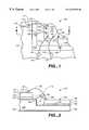
- FIG. 1is a partial top plan view of a semiconductor package made in accordance with the present invention.
- FIG. 2is a sectional view taken along the line 2 — 2 of FIG. 1;
- FIG. 3is a sectional view as in FIG. 2 wherein the anodization oxide layer of the heatspreader within the recess where the semiconductor die is mounted is removed to enhance thermal conduction between the die and the heatspreader;
- FIG. 4is a sectional profile view of an alternate type of semiconductor package made in accordance with the invention.
- FIGS. 1 and 2there is shown a partial top and sectional view, respectively, of a semiconductor package 100 made in accordance with the invention.
- the package 100includes a semiconductor die 102 having an active surface 103 (upper surface as oriented in FIG. 2) and a non-active surface 105 (lower surface as oriented in FIG. 2 ).
- the active surface 103includes a plurality of contact pads 104 thereon through which electrical contact is made with the electronic circuits that are embedded within the die 102 .
- these contact pads 104are located along the edges of the die 102 .
- At least one of the contact padscomprises a voltage potential pad 106 .
- the voltage potential padis electrically connected to a selected voltage source, e.g., Vdd, Vss, or ground, associated with the power source applied to the semiconductor die 102 in order to power the circuits embedded therein.
- the non-active surface 105 of the die 102is thermally bonded to a heatspreader 130 , typically through a layer 112 of a suitable thermal conductive paste, such as Ablebond 965, available from numerous commercial sources.
- the heatspreader 130is bonded to a package substrate 114 , typically using a layer 128 of contact cement, such as chomerics PSA, also commercially available.
- the package substrate 114includes conventional input/output (I/O) means for making electrical connection with the pins, balls, legs or leads (not shown) of the semiconductor package, depending upon the type of semiconductor package that is employed.
- I/O meansinclude a plurality of traces 118 , or other conductive members, that connect each pin, ball, leg or lead of the package to a respective connection pad 116 .
- the die 102is typically mounted within a recess 110 of the heatspreader 130 .
- Such recess 110is not required, but facilitates making the semiconductor package 100 thinner than it otherwise could be.
- Bonding wires 120connect each contact pad 104 of the IC die 102 to respective connection pads 116 of the package substrate 114 .
- Such bonding wires 120are typically connected to the contact pads 104 of the die using spot welds 123 , and connected to the connection pads 116 of the package substrate 114 using spot welds 121 , as is known in the art.
- Such connectionthus allows each pin, ball, leg or lead of the package 100 to be electrically connected with a corresponding contact pad 104 of the semiconductor die 102 .
- TABTape Automated Bonding
- such connectionmay be achieved using beams, rather than bonding wires, as is also known in the art.
- the heatspreader 130is made from aluminum, or an alloy of aluminum, which has been anodized to form an oxide layer 132 thereon.
- the manner of anodizing aluminumis known in the art. Such anodization is typically realized through an anodic process performed in a suitable electrolyte with the aluminum as the anode. Anodization of aluminum is typically carried out using an electrolyte such as chromic acid or sulfuric acid, but other electrolytes may also be used.
- the layer of aluminum oxide 132 that results from anodization processis typically a different color than is pure aluminum, thereby facilitating visual confirmation of the formation of the oxide layer 132 .
- the color of the anodization oxide layermay be selected to be a desired color, e.g., black, gray, or blue.
- Such layer 132advantageously provides a protective and insulative coating for the aluminum. This protective and insulative coating further allows the heatspreader to be electrically connected to ground, or other voltage potential, e.g., +5 volts, without fear or concern that the heatspreader might inadvertently short to another voltage or signal. Such connection, in turn, allows the heatspreader 130 to function as a voltage plane in order to improve the electrical performance characteristics of the semiconductor package.
- the heatspreader 130For the heatspreader 130 to function as a voltage plane, it must be bondable. That is, there must be a way to readily make electrical connection therewith. To facilitate such electrical connection, selected portions or areas of the oxide layer 132 are etched or milled away to expose small contact areas 124 of the aluminum heatspreader 130 . Bonding wires 122 , or equivalent, then connect at least one of the voltage potential pads 106 of the die 102 to the contact area 124 of the heatspreader 130 . Conventional spot welds 123 and 125 , or equivalent, may be used to secure the connection of the bonding wire 122 to the respective contact pads or areas.
- a variation of the semiconductor package 100 shown in FIGS. 1 and 2is illustrated as package 100 ′ in FIG. 3 .
- the package 100 ′ shown in FIG. 3is the same as that shown in FIGS. 1 and 2 except that the oxide layer 132 in the area of the recess 100 has been removed. Removal of the oxide layer 132 in the area where the non-active surface of the die 102 contacts the heatspreader through the thermally-conductive layer 112 may improve the thermal conduction properties of the package.
- a direct thermal path from the die 102 to the heatspreader 130 without having to pass through the oxide layer 132offers a somewhat improved thermal path (better thermal conductivity, or less thermal resistance) than does a thermal path that includes the oxide layer 132 .
- the semiconductor package 100is made using processes and techniques known in the art. The only difference is that the heatspreader is made from aluminum, instead of, e.g., copper. Once the aluminum heatspreader is formed it is anodized. Anodization places a protective film or layer 132 on the surface of the heatspreader. The thickness of the anodized layer 132 may be controlled to a certain extent during the anodization process, as is known in the art. After anodization, selected portions or areas 124 of the anodized heatspreader surface are removed, e.g., by grinding or milling away the oxide film or layer 132 , to thereby expose the base aluminum heatspreader 132 .
- the entire recess 100may be milled (or otherwise formed) in the heatspreader 30 after anodization has taken place. That is, a single, solid piece of aluminum, e.g., an aluminum sheet having a thickness of between about 0.25 and 2.50 mm, may be formed in the size and shape desired for the heatspreader of the package type that is to be made. Then such piece of aluminum may be anodized to form the oxide film or layer 132 thereon.
- a single, solid piece of aluminume.g., an aluminum sheet having a thickness of between about 0.25 and 2.50 mm
- the recess 110may then be formed in the heatspreader, e.g., to a depth of about 0.50 mm, which forming removes the oxide layer 132 in the area where the recess is formed.
- the die 102is then thermally and mechanically bonded to the heatspreader 130 using a thermally conductive layer of cement, or bonding compound, 112 .
- Wire bonds 120are then made, in conventional manner, in order to connect the contact pads 104 of the die 102 to the connection pads 116 of the package substrate 114 .
- Additional wire bonds 122are also installed in order to connect the voltage potential contact pads 106 of the die 102 to the exposed areas 124 of the heatspreader 130 .
- a suitable filler compound(not shown), e.g., epoxy, may then be used to cover the delicate wire bonds and to fill in the edges of the recess 110 , as is commonly practiced in the art.
- a flip-chip embodiment of the inventionis illustrated in the partial sectional view of FIG. 4, which shows a flip chip semiconductor package 200 .
- the flip chipincludes a die 102 ′ having an active surface 103 ′ that has a plurality of solder bumps 107 thereon.
- the solder bumps 107interface with suitable I/O means included within the substrate, as is known in the art, to electrically connect each solder bump 107 to a respective solder ball 109 located on a bottom surface of the package substrate 114 '. I/O connection with the die 102 ' is thus made through the array of solder balls 109 located on the bottom surface of the substrate 114 '.
- the flip-chip package 200includes a heatspreader 130 ′ having a lower surface that is in thermal contact with a non-active surface 105 ′ of the die 102 '. Such thermal contact is typically made using a thermal compound or thermal bonding agent 112 .
- a stiffener 140Around the periphery of the die 102 ′, the edges of the heatspreader 130 ′ are secured to the upper surface of the package substrate 114 using a stiffener 140 .
- the stiffener 140may be a separate element to which the heatspreader 130 ′ is attached, e.g., with fasteners or a suitable bonding cement; or the stiffener 140 may form an integral part of the heatspreader 130 '.
- the heatspreader 130 ′is anodized to form a protective oxide film or layer 132 thereon. While FIG. 4 shows the protective layer 132 as being on both sides of the heatspreader 130 ′, it is to be understood that it is also possible, and perhaps even preferable, to remove the oxide layer 132 on the underneath side of the heatspreader 130 ′ in that region where the die 102 ′ makes thermal contact therewith.
- the bottom edge 142 of the heatspreader 130 ′(or the bottom edge of the stiffener 140 , if used) is attached to the upper surface of the package substrate 114 ′ using any suitable fastening or attaching technique, e.g., using a conductive bonding cement or epoxy 144 .
- the oxide layer 132is removed from such bottom edge 142 to facilitate making electrical connection with the heatspreader.
- a contact trace or contact pads, connected to suitable voltage potential solder bumps on the active surface 103 ′ of the die 102 ′,are included within the package substrate 114 ′ so as to align with the bottom edge 142 of the heatspreader.
- the heatspreader 130 ′when the heatspreader 130 ′ is mounted on the package substrate 114 ′, such contact trace or contact pads make electrical connection with the bottom edge 142 , thereby electrically connecting the heatspreader 130 ′ to a selected voltage potential bump of the die 102 '.
- the heatspreader 130 ′may also function as a voltage plane within the semiconductor package 200 , thereby enhancing the electrical performance of the package.
- anodized aluminum heatspreader within a semiconductor package in accordance with the present inventionoffers several advantages.
- Third, being able to laminate the substrate package to the aluminum heatspreader using, e.g., an epoxyadvantageously provides a stronger bond than has heretofore been achievable when bonding to a gold- or nickel-plated copper heatspreader. Therefore, the reliability of the semiconductor package is improved.
- Fourth, the ability to wirebond directly to the heatspreaderallows the heatspreader to be used as a power or ground plane. The ability to incorporate power or ground planes within the semiconductor package significantly improves the electrical performance of the semiconductor package.
- anodized aluminum heatspreader within a semiconductor package in accordance with the present inventiona semiconductor package is provided that is lighter, less expensive, more reliable, and provides improved electrical performance, than has heretofore been achievable using a plated copper heatspreader as is common in the prior art.
- the anodized aluminum heatspreader of the present inventionprovides the opportunity to give the semiconductor package a desired color, e.g., black, which not only can improve heat dissipation of the package, but may also enhance the cosmetic appearance of the package.
- the oxide layer of the anodized aluminum heatspreaderis a good electrical insulator, the resulting semiconductor package offers the advantage of a robust metal exterior surface which is electrically insulated. Thus, inadvertent electrical contact with the exterior of the package will not cause any problems.
- the semiconductor package of the present inventionwith its anodized aluminum heatspreader, provides a similar exterior surface for attaching external heatsinks. Because such external heatsinks are typically made from aluminum, a good mechanical and thermal interface between the package and external heatsink results.
Landscapes
- Engineering & Computer Science (AREA)
- Computer Hardware Design (AREA)
- Microelectronics & Electronic Packaging (AREA)
- Power Engineering (AREA)
- Physics & Mathematics (AREA)
- Condensed Matter Physics & Semiconductors (AREA)
- General Physics & Mathematics (AREA)
- Chemical & Material Sciences (AREA)
- Materials Engineering (AREA)
- Cooling Or The Like Of Semiconductors Or Solid State Devices (AREA)
Abstract
Description
Claims (15)
Priority Applications (1)
| Application Number | Priority Date | Filing Date | Title |
|---|---|---|---|
| US09/053,357US6297550B1 (en) | 1998-04-01 | 1998-04-01 | Bondable anodized aluminum heatspreader for semiconductor packages |
Applications Claiming Priority (1)
| Application Number | Priority Date | Filing Date | Title |
|---|---|---|---|
| US09/053,357US6297550B1 (en) | 1998-04-01 | 1998-04-01 | Bondable anodized aluminum heatspreader for semiconductor packages |
Publications (1)
| Publication Number | Publication Date |
|---|---|
| US6297550B1true US6297550B1 (en) | 2001-10-02 |
Family
ID=21983660
Family Applications (1)
| Application Number | Title | Priority Date | Filing Date |
|---|---|---|---|
| US09/053,357Expired - LifetimeUS6297550B1 (en) | 1998-04-01 | 1998-04-01 | Bondable anodized aluminum heatspreader for semiconductor packages |
Country Status (1)
| Country | Link |
|---|---|
| US (1) | US6297550B1 (en) |
Cited By (10)
| Publication number | Priority date | Publication date | Assignee | Title |
|---|---|---|---|---|
| US6500698B2 (en)* | 1998-10-24 | 2002-12-31 | Hynix Semiconductor, Inc. | Method for fabricating a stacked semiconductor chip package |
| US6551114B2 (en)* | 2001-02-20 | 2003-04-22 | Advanced Micro Devices, Inc. | Semiconductor device having signal contacts and high current power contacts |
| US20030104652A1 (en)* | 2001-12-03 | 2003-06-05 | Vassoudevane Lebonheur | Semiconductor chip package and method of manufacturing same |
| US20050035452A1 (en)* | 2001-05-07 | 2005-02-17 | Broadcom Corporation | Die-up ball grid array package including a substrate having an opening and method for making the same |
| US20070254404A1 (en)* | 2006-05-01 | 2007-11-01 | Texas Instruments Incorporated | Semiconductor Package-on-Package System Including Integrated Passive Components |
| US20130020111A1 (en)* | 2011-07-20 | 2013-01-24 | Samsung Electro-Mechanics Co., Ltd. | Substrate for power module package and method for manufacturing the same |
| US20130099422A1 (en)* | 2010-06-23 | 2013-04-25 | Seidel, Inc. | Process for Selectively Removing a Coating Layer |
| CN103811431A (en)* | 2012-11-02 | 2014-05-21 | 辉达公司 | Open solder mask and or dielectric to increase lid or ring thickness and contact area to improve package coplanarity |
| US20180233463A1 (en)* | 2017-02-10 | 2018-08-16 | Behrooz Mehr | Grounding techniques for backside-biased semiconductor dice and related devices, systems and methods |
| US10186477B2 (en) | 2013-03-14 | 2019-01-22 | General Electric Company | Power overlay structure and method of making same |
Citations (26)
| Publication number | Priority date | Publication date | Assignee | Title |
|---|---|---|---|---|
| US3469017A (en)* | 1967-12-12 | 1969-09-23 | Rca Corp | Encapsulated semiconductor device having internal shielding |
| US4012768A (en)* | 1975-02-03 | 1977-03-15 | Motorola, Inc. | Semiconductor package |
| US4092697A (en)* | 1976-12-06 | 1978-05-30 | International Business Machines Corporation | Heat transfer mechanism for integrated circuit package |
| US5003429A (en) | 1990-07-09 | 1991-03-26 | International Business Machines Corporation | Electronic assembly with enhanced heat sinking |
| US5013871A (en)* | 1988-02-10 | 1991-05-07 | Olin Corporation | Kit for the assembly of a metal electronic package |
| JPH03218656A (en)* | 1990-01-24 | 1991-09-26 | Sumitomo Metal Mining Co Ltd | Heat dissipation material for semiconductor devices |
| US5225710A (en) | 1990-07-09 | 1993-07-06 | Lsi Logic Products Gmbh | Highly integrated electronic component with heat-conducting plate |
| US5289337A (en) | 1992-02-21 | 1994-02-22 | Intel Corporation | Heatspreader for cavity down multi-chip module with flip chip |
| US5367196A (en)* | 1992-09-17 | 1994-11-22 | Olin Corporation | Molded plastic semiconductor package including an aluminum alloy heat spreader |
| US5402006A (en)* | 1992-11-10 | 1995-03-28 | Texas Instruments Incorporated | Semiconductor device with enhanced adhesion between heat spreader and leads and plastic mold compound |
| US5578869A (en)* | 1994-03-29 | 1996-11-26 | Olin Corporation | Components for housing an integrated circuit device |
| US5583377A (en) | 1992-07-15 | 1996-12-10 | Motorola, Inc. | Pad array semiconductor device having a heat sink with die receiving cavity |
| US5596231A (en)* | 1991-08-05 | 1997-01-21 | Asat, Limited | High power dissipation plastic encapsulated package for integrated circuit die |
| US5621616A (en) | 1995-09-29 | 1997-04-15 | Lsi Logic Corporation | High density CMOS integrated circuit with heat transfer structure for improved cooling |
| US5629835A (en)* | 1994-07-19 | 1997-05-13 | Olin Corporation | Metal ball grid array package with improved thermal conductivity |
| US5650663A (en)* | 1995-07-03 | 1997-07-22 | Olin Corporation | Electronic package with improved thermal properties |
| US5701034A (en)* | 1994-05-03 | 1997-12-23 | Amkor Electronics, Inc. | Packaged semiconductor die including heat sink with locking feature |
| US5744863A (en)* | 1994-07-11 | 1998-04-28 | International Business Machines Corporation | Chip carrier modules with heat sinks attached by flexible-epoxy |
| US5796038A (en)* | 1997-06-16 | 1998-08-18 | Vlsi Technology, Inc. | Technique to produce cavity-up HBGA packages |
| US5796170A (en)* | 1996-02-15 | 1998-08-18 | Northern Telecom Limited | Ball grid array (BGA) integrated circuit packages |
| US5808870A (en)* | 1996-10-02 | 1998-09-15 | Stmicroelectronics, Inc. | Plastic pin grid array package |
| US5866943A (en)* | 1997-06-23 | 1999-02-02 | Lsi Logic Corporation | System and method for forming a grid array device package employing electomagnetic shielding |
| US5895966A (en)* | 1995-09-29 | 1999-04-20 | Analog Devices, Inc. | Integrated circuit and supply decoupling capacitor therefor |
| US5909056A (en)* | 1997-06-03 | 1999-06-01 | Lsi Logic Corporation | High performance heat spreader for flip chip packages |
| US5948542A (en)* | 1996-03-18 | 1999-09-07 | Mcdonnell Douglas Corporation | High-absorptance high-emittance anodic coating |
| US6111311A (en)* | 1997-12-26 | 2000-08-29 | Nec Corporation | Semiconductor device and method of forming the same |
- 1998
- 1998-04-01USUS09/053,357patent/US6297550B1/ennot_activeExpired - Lifetime
Patent Citations (26)
| Publication number | Priority date | Publication date | Assignee | Title |
|---|---|---|---|---|
| US3469017A (en)* | 1967-12-12 | 1969-09-23 | Rca Corp | Encapsulated semiconductor device having internal shielding |
| US4012768A (en)* | 1975-02-03 | 1977-03-15 | Motorola, Inc. | Semiconductor package |
| US4092697A (en)* | 1976-12-06 | 1978-05-30 | International Business Machines Corporation | Heat transfer mechanism for integrated circuit package |
| US5013871A (en)* | 1988-02-10 | 1991-05-07 | Olin Corporation | Kit for the assembly of a metal electronic package |
| JPH03218656A (en)* | 1990-01-24 | 1991-09-26 | Sumitomo Metal Mining Co Ltd | Heat dissipation material for semiconductor devices |
| US5003429A (en) | 1990-07-09 | 1991-03-26 | International Business Machines Corporation | Electronic assembly with enhanced heat sinking |
| US5225710A (en) | 1990-07-09 | 1993-07-06 | Lsi Logic Products Gmbh | Highly integrated electronic component with heat-conducting plate |
| US5596231A (en)* | 1991-08-05 | 1997-01-21 | Asat, Limited | High power dissipation plastic encapsulated package for integrated circuit die |
| US5289337A (en) | 1992-02-21 | 1994-02-22 | Intel Corporation | Heatspreader for cavity down multi-chip module with flip chip |
| US5583377A (en) | 1992-07-15 | 1996-12-10 | Motorola, Inc. | Pad array semiconductor device having a heat sink with die receiving cavity |
| US5367196A (en)* | 1992-09-17 | 1994-11-22 | Olin Corporation | Molded plastic semiconductor package including an aluminum alloy heat spreader |
| US5402006A (en)* | 1992-11-10 | 1995-03-28 | Texas Instruments Incorporated | Semiconductor device with enhanced adhesion between heat spreader and leads and plastic mold compound |
| US5578869A (en)* | 1994-03-29 | 1996-11-26 | Olin Corporation | Components for housing an integrated circuit device |
| US5701034A (en)* | 1994-05-03 | 1997-12-23 | Amkor Electronics, Inc. | Packaged semiconductor die including heat sink with locking feature |
| US5744863A (en)* | 1994-07-11 | 1998-04-28 | International Business Machines Corporation | Chip carrier modules with heat sinks attached by flexible-epoxy |
| US5629835A (en)* | 1994-07-19 | 1997-05-13 | Olin Corporation | Metal ball grid array package with improved thermal conductivity |
| US5650663A (en)* | 1995-07-03 | 1997-07-22 | Olin Corporation | Electronic package with improved thermal properties |
| US5621616A (en) | 1995-09-29 | 1997-04-15 | Lsi Logic Corporation | High density CMOS integrated circuit with heat transfer structure for improved cooling |
| US5895966A (en)* | 1995-09-29 | 1999-04-20 | Analog Devices, Inc. | Integrated circuit and supply decoupling capacitor therefor |
| US5796170A (en)* | 1996-02-15 | 1998-08-18 | Northern Telecom Limited | Ball grid array (BGA) integrated circuit packages |
| US5948542A (en)* | 1996-03-18 | 1999-09-07 | Mcdonnell Douglas Corporation | High-absorptance high-emittance anodic coating |
| US5808870A (en)* | 1996-10-02 | 1998-09-15 | Stmicroelectronics, Inc. | Plastic pin grid array package |
| US5909056A (en)* | 1997-06-03 | 1999-06-01 | Lsi Logic Corporation | High performance heat spreader for flip chip packages |
| US5796038A (en)* | 1997-06-16 | 1998-08-18 | Vlsi Technology, Inc. | Technique to produce cavity-up HBGA packages |
| US5866943A (en)* | 1997-06-23 | 1999-02-02 | Lsi Logic Corporation | System and method for forming a grid array device package employing electomagnetic shielding |
| US6111311A (en)* | 1997-12-26 | 2000-08-29 | Nec Corporation | Semiconductor device and method of forming the same |
Cited By (16)
| Publication number | Priority date | Publication date | Assignee | Title |
|---|---|---|---|---|
| US6500698B2 (en)* | 1998-10-24 | 2002-12-31 | Hynix Semiconductor, Inc. | Method for fabricating a stacked semiconductor chip package |
| US6551114B2 (en)* | 2001-02-20 | 2003-04-22 | Advanced Micro Devices, Inc. | Semiconductor device having signal contacts and high current power contacts |
| US20050035452A1 (en)* | 2001-05-07 | 2005-02-17 | Broadcom Corporation | Die-up ball grid array package including a substrate having an opening and method for making the same |
| US20030104652A1 (en)* | 2001-12-03 | 2003-06-05 | Vassoudevane Lebonheur | Semiconductor chip package and method of manufacturing same |
| US6975025B2 (en)* | 2001-12-03 | 2005-12-13 | Intel Corporation | Semiconductor chip package and method of manufacturing same |
| US20070254404A1 (en)* | 2006-05-01 | 2007-11-01 | Texas Instruments Incorporated | Semiconductor Package-on-Package System Including Integrated Passive Components |
| US7569918B2 (en)* | 2006-05-01 | 2009-08-04 | Texas Instruments Incorporated | Semiconductor package-on-package system including integrated passive components |
| US20130099422A1 (en)* | 2010-06-23 | 2013-04-25 | Seidel, Inc. | Process for Selectively Removing a Coating Layer |
| US20130020111A1 (en)* | 2011-07-20 | 2013-01-24 | Samsung Electro-Mechanics Co., Ltd. | Substrate for power module package and method for manufacturing the same |
| CN103811431A (en)* | 2012-11-02 | 2014-05-21 | 辉达公司 | Open solder mask and or dielectric to increase lid or ring thickness and contact area to improve package coplanarity |
| US9716051B2 (en)* | 2012-11-02 | 2017-07-25 | Nvidia Corporation | Open solder mask and or dielectric to increase lid or ring thickness and contact area to improve package coplanarity |
| US10186477B2 (en) | 2013-03-14 | 2019-01-22 | General Electric Company | Power overlay structure and method of making same |
| US10269688B2 (en) | 2013-03-14 | 2019-04-23 | General Electric Company | Power overlay structure and method of making same |
| US20180233463A1 (en)* | 2017-02-10 | 2018-08-16 | Behrooz Mehr | Grounding techniques for backside-biased semiconductor dice and related devices, systems and methods |
| US10741507B2 (en)* | 2017-02-10 | 2020-08-11 | Microchip Technology Incorporated | Grounding techniques for backside-biased semiconductor dice and related devices, systems and methods |
| US11476208B2 (en) | 2017-02-10 | 2022-10-18 | Microchip Technology Incorporated | Grounding techniques for backside-biased semiconductor dice and related devices, systems and methods |
Similar Documents
| Publication | Publication Date | Title |
|---|---|---|
| US6002169A (en) | Thermally enhanced tape ball grid array package | |
| US5293301A (en) | Semiconductor device and lead frame used therein | |
| US5583377A (en) | Pad array semiconductor device having a heat sink with die receiving cavity | |
| JP3526788B2 (en) | Method for manufacturing semiconductor device | |
| US5789809A (en) | Thermally enhanced micro-ball grid array package | |
| US5379186A (en) | Encapsulated electronic component having a heat diffusing layer | |
| US6919631B1 (en) | Structures for improving heat dissipation in stacked semiconductor packages | |
| US6528877B2 (en) | Semiconductor component having a chip carrier with openings for making contact | |
| US20020079593A1 (en) | Semiconductor package having heat sink attached to substrate | |
| US20050023677A1 (en) | Method for assembling a ball grid array package with multiple interposers | |
| US20020135080A1 (en) | Semiconductor device and method for fabricating same | |
| US20080029906A1 (en) | Semiconductor switching module and method | |
| KR20080031119A (en) | Semiconductor devices | |
| US20100270667A1 (en) | Semiconductor package with multiple chips and substrate in metal cap | |
| US6297550B1 (en) | Bondable anodized aluminum heatspreader for semiconductor packages | |
| JP2000294723A (en) | Stacked semiconductor device and its manufacture | |
| JPH0777258B2 (en) | Semiconductor device | |
| JPH09199629A (en) | Semiconductor device | |
| US20040159929A1 (en) | Semiconductor die package having two die paddles | |
| US6963129B1 (en) | Multi-chip package having a contiguous heat spreader assembly | |
| US6291893B1 (en) | Power semiconductor device for “flip-chip” connections | |
| JP3183064B2 (en) | Semiconductor device | |
| JPH09115956A (en) | Semiconductor device | |
| JP3065288B2 (en) | Semiconductor bare chip sealing method, semiconductor integrated circuit device, and method of manufacturing semiconductor integrated circuit device | |
| JPH03266456A (en) | Semiconductor chip heat dissipating member and semiconductor package |
Legal Events
| Date | Code | Title | Description |
|---|---|---|---|
| AS | Assignment | Owner name:LSI LOGIC CORPORATION, CALIFORNIA Free format text:ASSIGNMENT OF ASSIGNORS INTEREST;ASSIGNORS:CHIA, CHOK J.;VARIOT, PATRICK;ALAGARATNAM, MANIAM;REEL/FRAME:009107/0556 Effective date:19980331 | |
| STCF | Information on status: patent grant | Free format text:PATENTED CASE | |
| FPAY | Fee payment | Year of fee payment:4 | |
| FEPP | Fee payment procedure | Free format text:PAYOR NUMBER ASSIGNED (ORIGINAL EVENT CODE: ASPN); ENTITY STATUS OF PATENT OWNER: LARGE ENTITY | |
| FPAY | Fee payment | Year of fee payment:8 | |
| FPAY | Fee payment | Year of fee payment:12 | |
| AS | Assignment | Owner name:DEUTSCHE BANK AG NEW YORK BRANCH, AS COLLATERAL AG Free format text:PATENT SECURITY AGREEMENT;ASSIGNORS:LSI CORPORATION;AGERE SYSTEMS LLC;REEL/FRAME:032856/0031 Effective date:20140506 | |
| AS | Assignment | Owner name:LSI CORPORATION, CALIFORNIA Free format text:CHANGE OF NAME;ASSIGNOR:LSI LOGIC CORPORATION;REEL/FRAME:033102/0270 Effective date:20070406 | |
| AS | Assignment | Owner name:AVAGO TECHNOLOGIES GENERAL IP (SINGAPORE) PTE. LTD Free format text:ASSIGNMENT OF ASSIGNORS INTEREST;ASSIGNOR:LSI CORPORATION;REEL/FRAME:035390/0388 Effective date:20140814 | |
| AS | Assignment | Owner name:AGERE SYSTEMS LLC, PENNSYLVANIA Free format text:TERMINATION AND RELEASE OF SECURITY INTEREST IN PATENT RIGHTS (RELEASES RF 032856-0031);ASSIGNOR:DEUTSCHE BANK AG NEW YORK BRANCH, AS COLLATERAL AGENT;REEL/FRAME:037684/0039 Effective date:20160201 Owner name:LSI CORPORATION, CALIFORNIA Free format text:TERMINATION AND RELEASE OF SECURITY INTEREST IN PATENT RIGHTS (RELEASES RF 032856-0031);ASSIGNOR:DEUTSCHE BANK AG NEW YORK BRANCH, AS COLLATERAL AGENT;REEL/FRAME:037684/0039 Effective date:20160201 | |
| AS | Assignment | Owner name:BANK OF AMERICA, N.A., AS COLLATERAL AGENT, NORTH CAROLINA Free format text:PATENT SECURITY AGREEMENT;ASSIGNOR:AVAGO TECHNOLOGIES GENERAL IP (SINGAPORE) PTE. LTD.;REEL/FRAME:037808/0001 Effective date:20160201 Owner name:BANK OF AMERICA, N.A., AS COLLATERAL AGENT, NORTH Free format text:PATENT SECURITY AGREEMENT;ASSIGNOR:AVAGO TECHNOLOGIES GENERAL IP (SINGAPORE) PTE. LTD.;REEL/FRAME:037808/0001 Effective date:20160201 | |
| AS | Assignment | Owner name:AVAGO TECHNOLOGIES GENERAL IP (SINGAPORE) PTE. LTD., SINGAPORE Free format text:TERMINATION AND RELEASE OF SECURITY INTEREST IN PATENTS;ASSIGNOR:BANK OF AMERICA, N.A., AS COLLATERAL AGENT;REEL/FRAME:041710/0001 Effective date:20170119 Owner name:AVAGO TECHNOLOGIES GENERAL IP (SINGAPORE) PTE. LTD Free format text:TERMINATION AND RELEASE OF SECURITY INTEREST IN PATENTS;ASSIGNOR:BANK OF AMERICA, N.A., AS COLLATERAL AGENT;REEL/FRAME:041710/0001 Effective date:20170119 | |
| AS | Assignment | Owner name:BELL SEMICONDUCTOR, LLC, ILLINOIS Free format text:ASSIGNMENT OF ASSIGNORS INTEREST;ASSIGNORS:AVAGO TECHNOLOGIES GENERAL IP (SINGAPORE) PTE. LTD.;BROADCOM CORPORATION;REEL/FRAME:044886/0766 Effective date:20171208 | |
| AS | Assignment | Owner name:CORTLAND CAPITAL MARKET SERVICES LLC, AS COLLATERA Free format text:SECURITY INTEREST;ASSIGNORS:HILCO PATENT ACQUISITION 56, LLC;BELL SEMICONDUCTOR, LLC;BELL NORTHERN RESEARCH, LLC;REEL/FRAME:045216/0020 Effective date:20180124 | |
| AS | Assignment | Owner name:BELL NORTHERN RESEARCH, LLC, ILLINOIS Free format text:RELEASE BY SECURED PARTY;ASSIGNOR:CORTLAND CAPITAL MARKET SERVICES LLC;REEL/FRAME:059723/0382 Effective date:20220401 Owner name:BELL SEMICONDUCTOR, LLC, ILLINOIS Free format text:RELEASE BY SECURED PARTY;ASSIGNOR:CORTLAND CAPITAL MARKET SERVICES LLC;REEL/FRAME:059723/0382 Effective date:20220401 Owner name:HILCO PATENT ACQUISITION 56, LLC, ILLINOIS Free format text:RELEASE BY SECURED PARTY;ASSIGNOR:CORTLAND CAPITAL MARKET SERVICES LLC;REEL/FRAME:059723/0382 Effective date:20220401 |