US6297143B1 - Process for forming a bit-line in a MONOS device - Google Patents
Process for forming a bit-line in a MONOS deviceDownload PDFInfo
- Publication number
- US6297143B1 US6297143B1US09/426,743US42674399AUS6297143B1US 6297143 B1US6297143 B1US 6297143B1US 42674399 AUS42674399 AUS 42674399AUS 6297143 B1US6297143 B1US 6297143B1
- Authority
- US
- United States
- Prior art keywords
- semiconductor substrate
- trench
- line
- oxide layer
- bit
- Prior art date
- Legal status (The legal status is an assumption and is not a legal conclusion. Google has not performed a legal analysis and makes no representation as to the accuracy of the status listed.)
- Expired - Lifetime
Links
- 238000000034methodMethods0.000titleclaimsabstractdescription61
- 230000008569processEffects0.000titleclaimsabstractdescription56
- LPQOADBMXVRBNX-UHFFFAOYSA-Nac1ldcw0Chemical compoundCl.C1CN(C)CCN1C1=C(F)C=C2C(=O)C(C(O)=O)=CN3CCSC1=C32LPQOADBMXVRBNX-UHFFFAOYSA-N0.000titleclaimsabstract4
- 239000004065semiconductorSubstances0.000claimsabstractdescription45
- 239000000758substrateSubstances0.000claimsabstractdescription44
- VYPSYNLAJGMNEJ-UHFFFAOYSA-NSilicium dioxideChemical compoundO=[Si]=OVYPSYNLAJGMNEJ-UHFFFAOYSA-N0.000claimsabstractdescription21
- 229910052814silicon oxideInorganic materials0.000claimsabstractdescription17
- 229910052785arsenicInorganic materials0.000claimsdescription12
- RQNWIZPPADIBDY-UHFFFAOYSA-Narsenic atomChemical compound[As]RQNWIZPPADIBDY-UHFFFAOYSA-N0.000claimsdescription12
- ZOXJGFHDIHLPTG-UHFFFAOYSA-NBoronChemical compound[B]ZOXJGFHDIHLPTG-UHFFFAOYSA-N0.000claimsdescription8
- 229910052796boronInorganic materials0.000claimsdescription8
- 238000002955isolationMethods0.000claimsdescription6
- 238000004518low pressure chemical vapour depositionMethods0.000claimsdescription5
- 238000005137deposition processMethods0.000claimsdescription4
- 238000000623plasma-assisted chemical vapour depositionMethods0.000claimsdescription4
- 238000005530etchingMethods0.000claimsdescription3
- 238000007517polishing processMethods0.000claimsdescription3
- 229910021420polycrystalline siliconInorganic materials0.000claimsdescription3
- 230000006870functionEffects0.000claimsdescription2
- 238000000151depositionMethods0.000claims3
- 239000010410layerSubstances0.000description45
- 238000004519manufacturing processMethods0.000description11
- 230000003647oxidationEffects0.000description7
- 238000007254oxidation reactionMethods0.000description7
- 229910052581Si3N4Inorganic materials0.000description3
- 239000000463materialSubstances0.000description3
- HQVNEWCFYHHQES-UHFFFAOYSA-Nsilicon nitrideChemical compoundN12[Si]34N5[Si]62N3[Si]51N64HQVNEWCFYHHQES-UHFFFAOYSA-N0.000description3
- 230000005684electric fieldEffects0.000description2
- 238000005516engineering processMethods0.000description2
- 239000007943implantSubstances0.000description2
- 230000014759maintenance of locationEffects0.000description2
- 235000012239silicon dioxideNutrition0.000description2
- 239000000377silicon dioxideSubstances0.000description2
- CBENFWSGALASAD-UHFFFAOYSA-NOzoneChemical compound[O-][O+]=OCBENFWSGALASAD-UHFFFAOYSA-N0.000description1
- 238000012356Product developmentMethods0.000description1
- 230000002411adverseEffects0.000description1
- 238000011982device technologyMethods0.000description1
- 239000003989dielectric materialSubstances0.000description1
- 238000009792diffusion processMethods0.000description1
- 239000002355dual-layerSubstances0.000description1
- 239000000203mixtureSubstances0.000description1
- 238000012986modificationMethods0.000description1
- 230000004048modificationEffects0.000description1
- 238000005498polishingMethods0.000description1
- 238000005036potential barrierMethods0.000description1
- 238000012545processingMethods0.000description1
- 229910000077silaneInorganic materials0.000description1
- 229910052710siliconInorganic materials0.000description1
- 239000010703siliconSubstances0.000description1
Images

Classifications
- H—ELECTRICITY
- H10—SEMICONDUCTOR DEVICES; ELECTRIC SOLID-STATE DEVICES NOT OTHERWISE PROVIDED FOR
- H10B—ELECTRONIC MEMORY DEVICES
- H10B43/00—EEPROM devices comprising charge-trapping gate insulators
- H10B43/30—EEPROM devices comprising charge-trapping gate insulators characterised by the memory core region
- H—ELECTRICITY
- H10—SEMICONDUCTOR DEVICES; ELECTRIC SOLID-STATE DEVICES NOT OTHERWISE PROVIDED FOR
- H10B—ELECTRONIC MEMORY DEVICES
- H10B41/00—Electrically erasable-and-programmable ROM [EEPROM] devices comprising floating gates
Definitions
- the inventionrelates generally to the fabrication of semiconductor devices and, more particularly, to the fabrication of the dielectric layers in semiconductor devices.
- Non-volatile memory devicesare currently in widespread use in electronic components that require the retention of information when electrical power is terminated.
- Non-volatile memory devicesinclude read-only-memory (ROM), programmable-read-only memory (PROM), erasable-programmable-read-only-memory (EPROM), and electrically-erasable-programmable-read-only-memory (EEPROM) devices.
- EEPROM devicesdiffer from other non-volatile memory devices in that they can be electrically programmed and erased.
- Flash EEPROM devicesare similar to EEPROM devices in that memory cells can be programmed and erased electrically. However, Flash EEPROM devices enable the erasing of all memory cells in the device using a single electrical current pulse.
- EEPROM device technologyOne important dielectric material for the fabrication of the EEPROM is an oxide-nitride-oxide (ONO) structure.
- ONOoxide-nitride-oxide
- During programmingelectrical charge is transferred from the substrate to the silicon nitride layer in the ONO structure. Voltages are applied to the gate and drain creating vertical and lateral electric fields, which accelerate the electrons along the length of the channel. As the electrons move along the channel, some of them gain sufficient energy to jump over the potential barrier of the bottom silicon dioxide layer and become trapped in the silicon nitride layer. Electrons are trapped near the drain region because the electric fields are the strongest near the drain.
- a Flash device that utilizes the ONO structureis a Metal-Oxide-Nitride-Oxide-Silicon (MONOS) cell.
- MONOSMetal-Oxide-Nitride-Oxide-Silicon
- the variation of the arsenic concentrationcauses a twenty percent variation, or more, in the thickness of the bit-line oxidation layer. The variation in the bit-line oxidation layer produces unpredictable MONOS cell performance.
- MONOS cell technologyhas enabled memory designers to improve MONOS cells, numerous challenges exist in the fabrication of material layers within these devices.
- a fabrication process of MONOS cellsshould accommodate precise control of the thickness of a bit-line oxide layer. Accordingly, advances in MONOS cell fabrication technology are necessary to control bit-line oxide layer fabrication and insure high quality MONOS cell devices.
- a uniform bit-line oxide layeris formed to ensure a desired thickness of the bit-line oxide layer. Therefore, a quality of the MONOS cell is improved.
- a process for fabricating a buried bit-line structure for a MONOS cellincludes providing a semiconductor substrate and forming mask layer overlying the semiconductor substrate. Thereafter, an etch process is performed to form a trench in the semiconductor substrate. Next, the mask layer is removed and the trench formed in the semiconductor substrate is filled with a silicon oxide layer. To form a bit-line oxide layer, a chemical-mechanical-polishing process is utilized to planarize the silicon oxide layer and form a planar surface continuous with an upper surface of the semiconductor substrate.
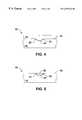
- FIG. 1illustrates, in cross-section, a portion of a semiconductor substrate containing a transistor that incorporates a bit-line oxide layer fabricated in accordance with the invention
- FIGS. 2-5illustrate, in cross-section, process steps for the fabrication of a buried bit-line structure in accordance with the invention.
- MONOS cell 10includes at least one buried bit-line 12 , a word-line 14 , and an ONO structure 16 , which function together to determine the location of a charge stored in memory.
- Bit-line 12 and ONO structure 16overlie a semiconductor substrate 18 .
- bit-line oxide layer 20Overlying the buried bit-line 12 is a bit-line oxide layer 20 , and also included are boron regions 22 and an arsenic region 24 .
- a MONOS devicenecessarily requires that an electrical charge is accurately introduced into a silicon nitride layer of the ONO structure 16 .
- a uniform bit-line oxidation processis necessary to accurately form the bit-line oxide layer 20 .
- a thickness of the bit-line oxide layer 20is accurately formed. Control of the bit-line oxide layer thickness which is obtained by the present invention can be better understood with the following description of a MONOS fabrication process carried out in accordance with the invention.
- a resist layer 26is formed to overlie the semiconductor substrate 18 .
- resist layer 26can be formed to overlie a thin oxide layer (not shown), which overlies semiconductor substrate 18 .
- a thin oxide layernot shown
- trench 27is formed in semiconductor substrate 18 for buried bit-line region 12 .
- trench 27has a depth of at least about 700 angstroms, and, more preferably, about 1000 angstroms, in semiconductor substrate 18 .
- bit-line oxide layer 20sufficiently isolates word-line 14 from buried bit-line region 12 .
- other etching processescan be used to fill the trench, such as a plasma etch process, an electron cyclotron etch process and the like.
- boron and arsenicare implanted into semiconductor substrate 18 , which forms boron regions 22 and arsenic region 24 respectively.
- the boronis implanted at a high angle, typically about twenty-five degrees to form boron regions 22 .
- arsenicis implanted at a low angle, typically about zero to about seven degrees, to form arsenic region 24 .
- Those skilled in the artwill appreciate that other angles can be used so long as the semiconductor substrate 18 is sufficiently doped after the implant process.
- silicon dioxidepreferably is deposited to form silicon oxide layer 28 to overfill the trench formed by the shallow trench isolation process.
- the trenchis filled using the plasma-enhanced-chemical-vapor-deposition (PECVD) process carried out at a temperature of about 400° C.
- PECVDplasma-enhanced-chemical-vapor-deposition
- the processtypically is carried out with a mixture of ozone and tetra-ethyl-ortho-silane (TEOS) gas, for a period of time sufficient to overfill the trench with silicon oxide.
- silicon oxide layer 28can be deposited by other processes, such as a low-pressure-chemical-vapor-deposition (LPCVD) process, a selective deposition process, a molecular beam deposition process, a high-density-plasma (HDP) deposition process, and the like.
- LPCVDlow-pressure-chemical-vapor-deposition
- HDPhigh-density-plasma
- a planarization processis carried out to remove portions of silicon oxide layer 28 overlying upper surface 30 of semiconductor substrate 18 .
- a chemical-mechanical-polishing (CMP) processis used to planarize silicon oxide layer 28 and to form a continuous surface with upper surface 30 of semiconductor substrate 18 .
- a planarization etch processcan be used to remove portions of silicon oxide layer 28 .
- the MONOS cell deviceis further completed by forming an ONO structure 16 to overlie semiconductor substrate 18 .
- polycrystalline silicon layer 14is formed to overlie the top oxide layer of ONO structure 16 , and bit-line oxide layer 20 .
- the polycrystalline silicon layer 14is deposited, for example, by the LPCVD process.
- the MONOS cell processingcontinues in a manner known in the art.
Landscapes
- Non-Volatile Memory (AREA)
- Semiconductor Memories (AREA)
Abstract
Description
Claims (17)
Priority Applications (1)
| Application Number | Priority Date | Filing Date | Title |
|---|---|---|---|
| US09/426,743US6297143B1 (en) | 1999-10-25 | 1999-10-25 | Process for forming a bit-line in a MONOS device |
Applications Claiming Priority (1)
| Application Number | Priority Date | Filing Date | Title |
|---|---|---|---|
| US09/426,743US6297143B1 (en) | 1999-10-25 | 1999-10-25 | Process for forming a bit-line in a MONOS device |
Publications (1)
| Publication Number | Publication Date |
|---|---|
| US6297143B1true US6297143B1 (en) | 2001-10-02 |
Family
ID=23692029
Family Applications (1)
| Application Number | Title | Priority Date | Filing Date |
|---|---|---|---|
| US09/426,743Expired - LifetimeUS6297143B1 (en) | 1999-10-25 | 1999-10-25 | Process for forming a bit-line in a MONOS device |
Country Status (1)
| Country | Link |
|---|---|
| US (1) | US6297143B1 (en) |
Cited By (23)
| Publication number | Priority date | Publication date | Assignee | Title |
|---|---|---|---|---|
| US6458642B1 (en)* | 2001-10-29 | 2002-10-01 | Macronix International Co., Ltd. | Method of fabricating a sonos device |
| US20040069990A1 (en)* | 2002-10-15 | 2004-04-15 | Matrix Semiconductor, Inc. | Thin film transistor with metal oxide layer and method of making same |
| US20060022249A1 (en)* | 2004-07-27 | 2006-02-02 | Se-Aug Jang | Memory device and method for fabricating the same |
| US7116577B2 (en) | 1997-08-01 | 2006-10-03 | Saifun Semiconductors Ltd | Two bit non-volatile electrically erasable and programmable semiconductor memory cell utilizing asymmetrical charge trapping |
| US7221138B2 (en) | 2005-09-27 | 2007-05-22 | Saifun Semiconductors Ltd | Method and apparatus for measuring charge pump output current |
| US7317633B2 (en) | 2004-07-06 | 2008-01-08 | Saifun Semiconductors Ltd | Protection of NROM devices from charge damage |
| US7352627B2 (en) | 2006-01-03 | 2008-04-01 | Saifon Semiconductors Ltd. | Method, system, and circuit for operating a non-volatile memory array |
| US7369440B2 (en) | 2005-01-19 | 2008-05-06 | Saifun Semiconductors Ltd. | Method, circuit and systems for erasing one or more non-volatile memory cells |
| US7420848B2 (en) | 2002-01-31 | 2008-09-02 | Saifun Semiconductors Ltd. | Method, system, and circuit for operating a non-volatile memory array |
| US7466594B2 (en) | 2004-08-12 | 2008-12-16 | Saifun Semiconductors Ltd. | Dynamic matching of signal path and reference path for sensing |
| US7518908B2 (en) | 2001-01-18 | 2009-04-14 | Saifun Semiconductors Ltd. | EEPROM array and method for operation thereof |
| US7532529B2 (en) | 2004-03-29 | 2009-05-12 | Saifun Semiconductors Ltd. | Apparatus and methods for multi-level sensing in a memory array |
| US7605579B2 (en) | 2006-09-18 | 2009-10-20 | Saifun Semiconductors Ltd. | Measuring and controlling current consumption and output current of charge pumps |
| US7638850B2 (en) | 2004-10-14 | 2009-12-29 | Saifun Semiconductors Ltd. | Non-volatile memory structure and method of fabrication |
| US7638835B2 (en) | 2006-02-28 | 2009-12-29 | Saifun Semiconductors Ltd. | Double density NROM with nitride strips (DDNS) |
| US7668017B2 (en) | 2005-08-17 | 2010-02-23 | Saifun Semiconductors Ltd. | Method of erasing non-volatile memory cells |
| US7675782B2 (en) | 2002-10-29 | 2010-03-09 | Saifun Semiconductors Ltd. | Method, system and circuit for programming a non-volatile memory array |
| US7692961B2 (en) | 2006-02-21 | 2010-04-06 | Saifun Semiconductors Ltd. | Method, circuit and device for disturb-control of programming nonvolatile memory cells by hot-hole injection (HHI) and by channel hot-electron (CHE) injection |
| US7738304B2 (en) | 2002-07-10 | 2010-06-15 | Saifun Semiconductors Ltd. | Multiple use memory chip |
| US7760554B2 (en) | 2006-02-21 | 2010-07-20 | Saifun Semiconductors Ltd. | NROM non-volatile memory and mode of operation |
| US7786512B2 (en) | 2005-07-18 | 2010-08-31 | Saifun Semiconductors Ltd. | Dense non-volatile memory array and method of fabrication |
| US7808818B2 (en) | 2006-01-12 | 2010-10-05 | Saifun Semiconductors Ltd. | Secondary injection for NROM |
| US8253452B2 (en) | 2006-02-21 | 2012-08-28 | Spansion Israel Ltd | Circuit and method for powering up an integrated circuit and an integrated circuit utilizing same |
Citations (2)
| Publication number | Priority date | Publication date | Assignee | Title |
|---|---|---|---|---|
| US5851881A (en)* | 1997-10-06 | 1998-12-22 | Taiwan Semiconductor Manufacturing Company, Ltd. | Method of making monos flash memory for multi-level logic |
| US6117730A (en)* | 1999-10-25 | 2000-09-12 | Advanced Micro Devices, Inc. | Integrated method by using high temperature oxide for top oxide and periphery gate oxide |
- 1999
- 1999-10-25USUS09/426,743patent/US6297143B1/ennot_activeExpired - Lifetime
Patent Citations (2)
| Publication number | Priority date | Publication date | Assignee | Title |
|---|---|---|---|---|
| US5851881A (en)* | 1997-10-06 | 1998-12-22 | Taiwan Semiconductor Manufacturing Company, Ltd. | Method of making monos flash memory for multi-level logic |
| US6117730A (en)* | 1999-10-25 | 2000-09-12 | Advanced Micro Devices, Inc. | Integrated method by using high temperature oxide for top oxide and periphery gate oxide |
Cited By (30)
| Publication number | Priority date | Publication date | Assignee | Title |
|---|---|---|---|---|
| US7116577B2 (en) | 1997-08-01 | 2006-10-03 | Saifun Semiconductors Ltd | Two bit non-volatile electrically erasable and programmable semiconductor memory cell utilizing asymmetrical charge trapping |
| US7405969B2 (en) | 1997-08-01 | 2008-07-29 | Saifun Semiconductors Ltd. | Non-volatile memory cell and non-volatile memory devices |
| US7518908B2 (en) | 2001-01-18 | 2009-04-14 | Saifun Semiconductors Ltd. | EEPROM array and method for operation thereof |
| US6458642B1 (en)* | 2001-10-29 | 2002-10-01 | Macronix International Co., Ltd. | Method of fabricating a sonos device |
| US7420848B2 (en) | 2002-01-31 | 2008-09-02 | Saifun Semiconductors Ltd. | Method, system, and circuit for operating a non-volatile memory array |
| US7738304B2 (en) | 2002-07-10 | 2010-06-15 | Saifun Semiconductors Ltd. | Multiple use memory chip |
| US20040069990A1 (en)* | 2002-10-15 | 2004-04-15 | Matrix Semiconductor, Inc. | Thin film transistor with metal oxide layer and method of making same |
| US6858899B2 (en) | 2002-10-15 | 2005-02-22 | Matrix Semiconductor, Inc. | Thin film transistor with metal oxide layer and method of making same |
| US7675782B2 (en) | 2002-10-29 | 2010-03-09 | Saifun Semiconductors Ltd. | Method, system and circuit for programming a non-volatile memory array |
| US7532529B2 (en) | 2004-03-29 | 2009-05-12 | Saifun Semiconductors Ltd. | Apparatus and methods for multi-level sensing in a memory array |
| US7317633B2 (en) | 2004-07-06 | 2008-01-08 | Saifun Semiconductors Ltd | Protection of NROM devices from charge damage |
| US7338864B2 (en)* | 2004-07-27 | 2008-03-04 | Hynix Semiconductor Inc. | Memory device and method for fabricating the same |
| US20060160286A1 (en)* | 2004-07-27 | 2006-07-20 | Eung-Rim Hwang | Memory device and method for fabricating the same |
| US7045846B2 (en)* | 2004-07-27 | 2006-05-16 | Hynix Semiconductor Inc. | Memory device and method for fabricating the same |
| US20060022249A1 (en)* | 2004-07-27 | 2006-02-02 | Se-Aug Jang | Memory device and method for fabricating the same |
| US7466594B2 (en) | 2004-08-12 | 2008-12-16 | Saifun Semiconductors Ltd. | Dynamic matching of signal path and reference path for sensing |
| US7638850B2 (en) | 2004-10-14 | 2009-12-29 | Saifun Semiconductors Ltd. | Non-volatile memory structure and method of fabrication |
| US7964459B2 (en) | 2004-10-14 | 2011-06-21 | Spansion Israel Ltd. | Non-volatile memory structure and method of fabrication |
| US7468926B2 (en) | 2005-01-19 | 2008-12-23 | Saifun Semiconductors Ltd. | Partial erase verify |
| US7369440B2 (en) | 2005-01-19 | 2008-05-06 | Saifun Semiconductors Ltd. | Method, circuit and systems for erasing one or more non-volatile memory cells |
| US7786512B2 (en) | 2005-07-18 | 2010-08-31 | Saifun Semiconductors Ltd. | Dense non-volatile memory array and method of fabrication |
| US7668017B2 (en) | 2005-08-17 | 2010-02-23 | Saifun Semiconductors Ltd. | Method of erasing non-volatile memory cells |
| US7221138B2 (en) | 2005-09-27 | 2007-05-22 | Saifun Semiconductors Ltd | Method and apparatus for measuring charge pump output current |
| US7352627B2 (en) | 2006-01-03 | 2008-04-01 | Saifon Semiconductors Ltd. | Method, system, and circuit for operating a non-volatile memory array |
| US7808818B2 (en) | 2006-01-12 | 2010-10-05 | Saifun Semiconductors Ltd. | Secondary injection for NROM |
| US7692961B2 (en) | 2006-02-21 | 2010-04-06 | Saifun Semiconductors Ltd. | Method, circuit and device for disturb-control of programming nonvolatile memory cells by hot-hole injection (HHI) and by channel hot-electron (CHE) injection |
| US7760554B2 (en) | 2006-02-21 | 2010-07-20 | Saifun Semiconductors Ltd. | NROM non-volatile memory and mode of operation |
| US8253452B2 (en) | 2006-02-21 | 2012-08-28 | Spansion Israel Ltd | Circuit and method for powering up an integrated circuit and an integrated circuit utilizing same |
| US7638835B2 (en) | 2006-02-28 | 2009-12-29 | Saifun Semiconductors Ltd. | Double density NROM with nitride strips (DDNS) |
| US7605579B2 (en) | 2006-09-18 | 2009-10-20 | Saifun Semiconductors Ltd. | Measuring and controlling current consumption and output current of charge pumps |
Similar Documents
| Publication | Publication Date | Title |
|---|---|---|
| US6297143B1 (en) | Process for forming a bit-line in a MONOS device | |
| US6117733A (en) | Poly tip formation and self-align source process for split-gate flash cell | |
| US6960505B2 (en) | Method for manufacturing a multi-bit memory cell | |
| US7442987B2 (en) | Non-volatile memory devices including divided charge storage structures | |
| US7342280B2 (en) | Non-volatile memory and method of fabricating the same | |
| US6538277B2 (en) | Split-gate flash cell | |
| US6436766B1 (en) | Process for fabricating high density memory cells using a polysilicon hard mask | |
| US6248635B1 (en) | Process for fabricating a bit-line in a monos device using a dual layer hard mask | |
| US6380035B1 (en) | Poly tip formation and self-align source process for split-gate flash cell | |
| US6017795A (en) | Method of fabricating buried source to shrink cell dimension and increase coupling ratio in split-gate flash | |
| US20060216891A1 (en) | Non-volatile memory device and method of fabricating the same | |
| KR20030019917A (en) | Memory cell, memory cell device and method for the production thereof | |
| JP2008530771A (en) | Electrically rewritable non-volatile memory cell for storing multiple data and manufacturing method thereof | |
| US20040119109A1 (en) | Non-volatile memory device having improved programming and erasing characteristics and method of fabricating the same | |
| US20060186480A1 (en) | Charge-trapping memory device and method for production | |
| US6326268B1 (en) | Method of fabricating a MONOS flash cell using shallow trench isolation | |
| US5990515A (en) | Trenched gate non-volatile semiconductor device and method with corner doping and sidewall doping | |
| US20030124800A1 (en) | Method of forming a floating gate in a flash memory device | |
| US6440798B1 (en) | Method of forming a mixed-signal circuit embedded NROM memory and MROM memory | |
| US20040156247A1 (en) | Method of fabricating non-volatile memory device | |
| US6969653B2 (en) | Methods of manufacturing and-type flash memory devices | |
| EP1345273A1 (en) | Dual bit multi-level ballistic monos memory, and manufacturing method, programming, and operation process for the memory | |
| US6465303B1 (en) | Method of manufacturing spacer etch mask for silicon-oxide-nitride-oxide-silicon (SONOS) type nonvolatile memory | |
| US7041545B2 (en) | Method for producing semiconductor memory devices and integrated memory device | |
| US6242305B1 (en) | Process for fabricating a bit-line using buried diffusion isolation |
Legal Events
| Date | Code | Title | Description |
|---|---|---|---|
| AS | Assignment | Owner name:ADVANCED MICRO DEVICES, INC., CALIFORNIA Free format text:ASSIGNMENT OF ASSIGNORS INTEREST;ASSIGNORS:FOOTE, DAVID K.;RANGARAJAN, BHARATH;WANG, FEI;AND OTHERS;REEL/FRAME:010564/0409;SIGNING DATES FROM 20000112 TO 20000204 | |
| STCF | Information on status: patent grant | Free format text:PATENTED CASE | |
| FPAY | Fee payment | Year of fee payment:4 | |
| AS | Assignment | Owner name:SPANSION INC., CALIFORNIA Free format text:ASSIGNMENT OF ASSIGNORS INTEREST;ASSIGNOR:ADVANCED MICRO DEVICES, INC.;REEL/FRAME:019047/0526 Effective date:20070131 | |
| AS | Assignment | Owner name:SPANSION LLC, CALIFORNIA Free format text:ASSIGNMENT OF ASSIGNORS INTEREST;ASSIGNOR:SPANSION INC.;REEL/FRAME:019069/0187 Effective date:20070131 | |
| FPAY | Fee payment | Year of fee payment:8 | |
| AS | Assignment | Owner name:BARCLAYS BANK PLC,NEW YORK Free format text:SECURITY AGREEMENT;ASSIGNORS:SPANSION LLC;SPANSION INC.;SPANSION TECHNOLOGY INC.;AND OTHERS;REEL/FRAME:024522/0338 Effective date:20100510 Owner name:BARCLAYS BANK PLC, NEW YORK Free format text:SECURITY AGREEMENT;ASSIGNORS:SPANSION LLC;SPANSION INC.;SPANSION TECHNOLOGY INC.;AND OTHERS;REEL/FRAME:024522/0338 Effective date:20100510 | |
| FPAY | Fee payment | Year of fee payment:12 | |
| AS | Assignment | Owner name:SPANSION INC., CALIFORNIA Free format text:RELEASE BY SECURED PARTY;ASSIGNOR:BARCLAYS BANK PLC;REEL/FRAME:035201/0159 Effective date:20150312 Owner name:SPANSION TECHNOLOGY LLC, CALIFORNIA Free format text:RELEASE BY SECURED PARTY;ASSIGNOR:BARCLAYS BANK PLC;REEL/FRAME:035201/0159 Effective date:20150312 Owner name:SPANSION LLC, CALIFORNIA Free format text:RELEASE BY SECURED PARTY;ASSIGNOR:BARCLAYS BANK PLC;REEL/FRAME:035201/0159 Effective date:20150312 | |
| AS | Assignment | Owner name:MORGAN STANLEY SENIOR FUNDING, INC., NEW YORK Free format text:SECURITY INTEREST;ASSIGNORS:CYPRESS SEMICONDUCTOR CORPORATION;SPANSION LLC;REEL/FRAME:035240/0429 Effective date:20150312 | |
| AS | Assignment | Owner name:CYPRESS SEMICONDUCTOR CORPORATION, CALIFORNIA Free format text:ASSIGNMENT OF ASSIGNORS INTEREST;ASSIGNOR:SPANSION, LLC;REEL/FRAME:036031/0691 Effective date:20150601 | |
| AS | Assignment | Owner name:CYPRESS SEMICONDUCTOR CORPORATION, CALIFORNIA Free format text:PARTIAL RELEASE OF SECURITY INTEREST IN PATENTS;ASSIGNOR:MORGAN STANLEY SENIOR FUNDING, INC., AS COLLATERAL AGENT;REEL/FRAME:039708/0001 Effective date:20160811 Owner name:SPANSION LLC, CALIFORNIA Free format text:PARTIAL RELEASE OF SECURITY INTEREST IN PATENTS;ASSIGNOR:MORGAN STANLEY SENIOR FUNDING, INC., AS COLLATERAL AGENT;REEL/FRAME:039708/0001 Effective date:20160811 | |
| AS | Assignment | Owner name:MONTEREY RESEARCH, LLC, CALIFORNIA Free format text:ASSIGNMENT OF ASSIGNORS INTEREST;ASSIGNOR:CYPRESS SEMICONDUCTOR CORPORATION;REEL/FRAME:040911/0238 Effective date:20160811 | |
| AS | Assignment | Owner name:MORGAN STANLEY SENIOR FUNDING, INC., NEW YORK Free format text:CORRECTIVE ASSIGNMENT TO CORRECT THE 8647899 PREVIOUSLY RECORDED ON REEL 035240 FRAME 0429. ASSIGNOR(S) HEREBY CONFIRMS THE SECURITY INTERST;ASSIGNORS:CYPRESS SEMICONDUCTOR CORPORATION;SPANSION LLC;REEL/FRAME:058002/0470 Effective date:20150312 |