US6297095B1 - Memory device that includes passivated nanoclusters and method for manufacture - Google Patents
Memory device that includes passivated nanoclusters and method for manufactureDownload PDFInfo
- Publication number
- US6297095B1 US6297095B1US09/596,399US59639900AUS6297095B1US 6297095 B1US6297095 B1US 6297095B1US 59639900 AUS59639900 AUS 59639900AUS 6297095 B1US6297095 B1US 6297095B1
- Authority
- US
- United States
- Prior art keywords
- nanoclusters
- layer
- silicon
- oxide
- tunnel dielectric
- Prior art date
- Legal status (The legal status is an assumption and is not a legal conclusion. Google has not performed a legal analysis and makes no representation as to the accuracy of the status listed.)
- Expired - Lifetime
Links
Images


Classifications
- B—PERFORMING OPERATIONS; TRANSPORTING
- B82—NANOTECHNOLOGY
- B82Y—SPECIFIC USES OR APPLICATIONS OF NANOSTRUCTURES; MEASUREMENT OR ANALYSIS OF NANOSTRUCTURES; MANUFACTURE OR TREATMENT OF NANOSTRUCTURES
- B82Y10/00—Nanotechnology for information processing, storage or transmission, e.g. quantum computing or single electron logic
- H—ELECTRICITY
- H10—SEMICONDUCTOR DEVICES; ELECTRIC SOLID-STATE DEVICES NOT OTHERWISE PROVIDED FOR
- H10D—INORGANIC ELECTRIC SEMICONDUCTOR DEVICES
- H10D30/00—Field-effect transistors [FET]
- H10D30/01—Manufacture or treatment
- H10D30/014—Manufacture or treatment of FETs having zero-dimensional [0D] or one-dimensional [1D] channels, e.g. quantum wire FETs, single-electron transistors [SET] or Coulomb blockade transistors
- H—ELECTRICITY
- H10—SEMICONDUCTOR DEVICES; ELECTRIC SOLID-STATE DEVICES NOT OTHERWISE PROVIDED FOR
- H10D—INORGANIC ELECTRIC SEMICONDUCTOR DEVICES
- H10D30/00—Field-effect transistors [FET]
- H10D30/60—Insulated-gate field-effect transistors [IGFET]
- H10D30/68—Floating-gate IGFETs
- H10D30/688—Floating-gate IGFETs programmed by two single electrons
- H—ELECTRICITY
- H10—SEMICONDUCTOR DEVICES; ELECTRIC SOLID-STATE DEVICES NOT OTHERWISE PROVIDED FOR
- H10D—INORGANIC ELECTRIC SEMICONDUCTOR DEVICES
- H10D64/00—Electrodes of devices having potential barriers
- H10D64/01—Manufacture or treatment
- H10D64/031—Manufacture or treatment of data-storage electrodes
- H10D64/035—Manufacture or treatment of data-storage electrodes comprising conductor-insulator-conductor-insulator-semiconductor structures
- H—ELECTRICITY
- H10—SEMICONDUCTOR DEVICES; ELECTRIC SOLID-STATE DEVICES NOT OTHERWISE PROVIDED FOR
- H10D—INORGANIC ELECTRIC SEMICONDUCTOR DEVICES
- H10D64/00—Electrodes of devices having potential barriers
- H10D64/01—Manufacture or treatment
- H10D64/031—Manufacture or treatment of data-storage electrodes
- H10D64/037—Manufacture or treatment of data-storage electrodes comprising charge-trapping insulators
Definitions
- the inventionrelates generally to semiconductor devices and more particularly to a semiconductor memory device and a process for forming such a semiconductor memory device.
- EEPROMElectrically erasable programmable read only memory
- EEPROM device structurescommonly include a floating gate that has charge storage capabilities. Charge can be forced into the floating gate structure or removed from the floating gate structure using control voltages. The conductivity of the channel underlying the floating gate is significantly altered by the presence of charges stored in the floating gate. The difference in conductivity due to a charged or uncharged floating gate can be current sensed, thus allowing binary memory states to be determined. The conductivity difference is also represented by shift in the threshold voltage (V T ) associated with the device in the two different states.
- V Tthreshold voltage
- the operating voltages of such semiconductor devicesare often reduced in order to suit low power applications. It is desirable for such operating voltage reductions to be accomplished while ensuring that the speed and functionality of the devices is maintained or improved.
- a controlling factor in the operating voltages required to program and erase devices that include floating gatesis the thickness of the tunnel oxide through which carriers are exchanged between the floating gate and the underlying channel region.
- the floating gateis formed from a uniform layer of material such as polysilicon.
- a thin tunnel dielectric layer beneath the floating gatepresents the problem of charge leakage from the floating gate to the underlying channel through defects in the thin tunnel dielectric layer. Such charge leakage can lead to degradation of the memory state stored within the device and is therefore undesirable.
- the thickness of tunnel dielectricis often increased.
- thicker tunnel dielectricrequires higher (programming and erasing) voltages for storing and removing charge from the floating gate as the charge carriers must pass through the thicker tunnel dielectric.
- higher programming voltagesrequire the implementation of charge pumps on integrated circuits in order to increase the supply voltage to meet programming voltage requirements. Such charge pumps consume a significant amount of die area for the integrated circuit and therefore reduce the memory array area efficiency and increase overall costs.
- the uniform layer of material used for the floating gatemay be replaced with a plurality of nanoclusters, which operate as isolated charge storage elements.
- Such nanoclustersare also often referred to as nanocrystals, as they may be formed of silicon crystals.
- the plurality of nanoclustersprovide adequate charge storage capacity while remaining physically isolated from each other such that any leakage occurring with respect to a single nanoclusters via a local underlying defect does not cause charge to be drained from other nanoclusters (by controlling average spacing between nanoclusters, it can be ensured that there is no lateral charge flow between nanoclusters in the floating gate).
- thinner tunnel dielectricscan be used in these device structures. The effects of leakage occurring in such thin tunnel dielectric devices does not cause the loss of state information that occurs in devices that include a uniform-layer floating gate.
- a limiting factor in fabrication of devices that include floating gates made up of a plurality of nanoclustersrelates to controlling of the size, density, and uniformity of the nanoclusters within the floating gate structure.
- the density of the nanoclustersis important in the determination of the change in the threshold voltage for the device between the states where the floating gate is charged or discharged. Higher densities are desirable as they lead to an increased change in threshold voltage when the density of charges per storage element is fixed.
- Prior art techniques for forming nanoclusters on the oxide tunnel dielectricwere limited to a density of approximately 5 ⁇ 10 11 nanoclusters per cm 2 . With such a limited density of isolated storage elements, the charge density per nanocluster, or number of carriers that each nanocluster must retain, is forced to an elevated level.
- the higher storage density per nanoclustertypically leads to charge loss from individual nanoclusters, thus degrading the overall charge retention characteristics of the floating gate.
- lower nanocluster densitiesrequire longer programming times as a longer time period is required for forcing subsequent charge carriers into each nanocluster after an initial carrier has been stored.
- the time required for adding subsequent carrierscontinues to increase as the charge density per nanocluster is elevated.
- ion implantationis used to implant silicon atoms into a dielectric material. Following implantation, an annealing step causes these implanted silicon atoms to group together through phase separation to form the nanoclusters. Problems arise using such a technique due to the difficulty in controlling the depth at which the silicon nanoclusters are formed due to the phase segregation in the dielectric material. Because the depth at which the isolation storage elements are formed dramatically affects the electrical characteristics of the resulting device, ion implantation does not provide the level of control desired in a manufacturing situation.
- a thin layer of amorphous siliconis deposited on the tunnel dielectric material.
- a subsequent annealing stepis used to recrystalize the amorphous silicon into the nanoclusters.
- the layer of amorphous siliconshould be deposited such that it is on the order of 7-10 angstroms in thickness. Deposition of such thin layers of amorphous silicon is hard to control and therefore impractical in a manufacturing process. In addition to such control issues, additional problems may arise due to preexisting crystalline zones within the amorphous silicon layer. Such preexisting crystallites serve as nucleation sites for crystal growth, which deleteriously interferes with the spontaneous crystal growth desired for formation of the nanoclusters.
- CVDchemical vapor deposition
- LPCVDlow pressure chemical vapor deposition
- Such prior art LPCVD techniquestypically involve a very short deposition time period, on the order of approximately 10-30 seconds. Part of this deposition time period includes an incubation period where an adequate number of silicon atoms are generated on the surface of the dielectric prior to the commencement of the clustering activity that forms the crystalline structures of the nanoclusters. The remaining portion of the time is used to nucleate and grow the nanoclusters to the desired size.
- FIG. 1includes a graph that illustrates curves associated with nanocluster formation, where such curves plot nanocluster density versus time during CVD processing;
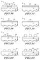
- FIG. 2illustrates a cross-sectional view of a portion of a semiconductor substrate that includes a formed layer of tunnel dielectric
- FIG. 3illustrates a cross-sectional view of the portion of the semiconductor substrate of FIG. 2 following formation of an overlying nitrogen-containing layer in accordance with a particular embodiment of the present invention
- FIG. 4illustrates a cross-sectional view of the portion of the semiconductor substrate of FIG. 2, including a representation of the initial molecular bonding structure at the surface of the tunnel dielectric layer;
- FIG. 5illustrates a cross-sectional view of the portion of the semiconductor substrate of FIG. 4 following alteration of the molecular bonding structure at the surface of the tunnel dielectric layer in accordance with a particular embodiment of the present invention
- FIG. 6illustrates a cross-sectional view of the portion of the semiconductor substrate of FIG. 2 where nanocluster nucleation has been initiated in accordance with a particular embodiment of the present invention
- FIGS. 7-9illustrate cross-sectional views of the portion of the semiconductor substrate of FIG. 6 at subsequent time intervals corresponding to the formation of the nanoclusters in accordance with a particular embodiment of the present invention
- FIG. 10illustrates a cross-sectional view of the semiconductor substrate portion of FIG. 9 where the nanoclusters have been partially or fully relaxed to equilibrium with the surface of the tunnel dielectric layer in accordance with a particular embodiment of the present invention
- FIG. 11illustrates a cross-sectional view of the semiconductor substrate portion of FIG. 10 upon which a control dielectric layer has been formed in accordance with a particular embodiment of the present invention
- FIG. 12illustrates a cross-sectional view of the semiconductor substrate portion of FIG. 11 upon which a gate material layer has been formed in accordance with a particular embodiment of the present invention
- FIG. 13illustrates a cross-sectional view of the semiconductor substrate portion of FIG. 12 where the gate material layer has been patterned to form a gate electrode in accordance with a particular embodiment of the present invention
- FIG. 14illustrates a cross-sectional view of the semiconductor substrate portion of FIG. 13 where a portion of the control dielectric layer has been selectively removed in accordance with a particular embodiment of the present invention
- FIG. 15illustrates a cross-sectional view of the semiconductor substrate portion of FIG. 14 after selective removal of portions of the tunnel dielectric layer, the plurality of nanoclusters, and the control dielectric layer in accordance with the particular embodiment of the present invention
- FIG. 16illustrates a cross-sectional view of the semiconductor substrate portion of FIG. 15 where spacers, a source region, and a drain region have been formed for a semiconductor device in accordance with a particular embodiment of the present invention
- FIGS. 17-19illustrate cross-sectional views of the semiconductor substrate portion of FIG. 3 after sequential steps used to form a nitrogen-containing layer section overlying the tunnel dielectric layer in accordance with a particular embodiment of the present invention
- FIG. 20illustrates a cross-sectional view of the semiconductor substrate portion of FIG. 19 following selective growth of nanoclusters in accordance with a particular embodiment of the present invention
- FIG. 21illustrates an expanded cross-sectional view of a plurality of nanoclusters formed on a tunnel dielectric layer in accordance with a particular embodiment of the present invention
- FIG. 22illustrates an expanded cross-sectional view of the plurality of nanoclusters of FIG. 21 following partial or complete relaxation with the surface of the underlying tunnel dielectric layer in accordance with a particular embodiment of the Present invention
- FIG. 23illustrates an expanded cross-sectional view of the nanoclusters of FIG. 22 where the nanoclusters have been encapsulated in an encapsulation layer in accordance with a particular embodiment of the present invention
- FIG. 24illustrates an expanded cross-sectional view of the structure of FIG. 23 where a control dielectric layer has been formed overlying the tunnel dielectric layer and the encapsulated nanoclusters in accordance with a particular embodiment of the present invention
- FIG. 25illustrates an expanded cross-sectional view of the nanoclusters of FIG. 22 following formation of a thin dielectric layer overlying the plurality of nanoclusters in accordance with a particular embodiment of the present invention
- FIG. 26illustrates an expanded cross-sectional view of the structure of FIG. 25 following formation of a control dielectric layer overlying the thin dielectric layer in accordance with a particular embodiment of the present invention
- FIG. 27illustrates an expanded cross-sectional view of the structure of FIG. 22 following formation of a multi-layered control dielectric overlying the plurality of nanoclusters
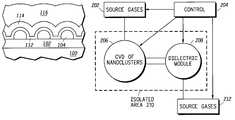
- FIG. 28illustrates a schematic diagram of a processing apparatus for forming a tunnel dielectric layer, a plurality of nanoclusters overlying the tunnel dielectric layer, and a portion or the entirety of an overlying control dielectric in accordance with a particular embodiment of the present invention.
- the present inventionpertains to a semiconductor memory device with a floating gate that includes a plurality of nanoclusters and techniques useful in the manufacturing of such a device.
- the deviceis formed by first providing a semiconductor substrate upon which a tunnel dielectric layer is formed. A plurality of nanoclusters is then grown on the tunnel dielectric layer. After growth of the nanoclusters, a control dielectric layer is formed over the nanoclusters.
- the nanoclustersmay be encapsulated or passivated prior to formation of the control dielectric layer. Such encapsulation may include forming a thin layer of nitride on the nanoclusters.
- a gate electrodeis then formed over the control dielectric, and portions of the control dielectric, the plurality of nanoclusters, and the gate dielectric that do not underlie the gate electrode are selectively removed.
- source and drain regionsare formed by implantation in the semiconductor layer such that a channel region is formed between the source and drain regions underlying the gate electrode.
- the density of nanoclusters included in the floating gate structurecan be closely controlled.
- references to LPCVD processingdescribe processing that may be performed using LPCVD or RTCVD processing techniques.
- a multistep processmay be utilized to ensure proper nucleation and growth selectivity for different phases of the nanocluster formation. As such, desired nanocluster densities can be achieved while ensuring uniformity in size and density in a manufacturable process.
- UHVCVDis utilized to grow the nanocluster structures
- additional advantagesare achieved due to the reduction in background contamination in the environment within which the nanocluster formation occurs. Similar optimizations to the formation of the nanoclusters that were utilized in LPCVD techniques can be employed in UHVCVD techniques to produce the desired resulting nanocluster structures.
- UHVCVD techniqueseven lower pressures than those present in LPCVD techniques can provide a further reduction in growth kinetics such that a higher level of control is obtained over the nanocluster formation.
- potential gradients in nanocluster growth rates due to precursor gas depletion effectsare further minimized.
- FIG. 1illustrates a graph that shows the general evolution of the nanoclusters during the nucleation and growth phases as a function of time.
- Two curves 302 and 312are illustrated in FIG. 1 .
- the curve 302corresponds to nanocluster development consistent with prior art techniques in which higher temperatures and shorter growth time periods produced through a single step deposition process resulted in a limited level of control over nanocluster growth.
- the parameters associated with such prior art techniquesprovide a lack of control of the selectivity of nucleation to growth with regard to nanocluster formation during all phases of the one step process to which the curve 302 corresponds.
- the curve 302 corresponding to the prior art deposition techniquebegins with a brief incubation phase where silicon atoms begin to be deposited on the tunnel dielectric layer. Once enough silicon atoms have been deposited on the dielectric material, nucleation begins to occur. Due to the fact that higher temperatures are used in conjunction with the prior art technique, the surface diffusion rate of silicon atoms present on the dielectric layer will be higher than that in a lower temperature environment. The size of the stable critical nucleus is also higher at the higher deposition temperature. The growth of the already formed nuclei is also higher at the higher temperature.
- the silicon atoms arriving on the surface of the dielectricmust move through a longer diffusion distance before they are either captured by an already existing nucleus or they combine with other diffusing silicon atoms to form a stable nucleus.
- the probability of capture of a silicon atom by an existing nucleusis higher at higher temperature due to longer diffusion distances, hence the growth rate of nuclei dominates the nucleation rate. This type of limited nucleation and rapid growth is undesirable as it results in smaller numbers of large nanoclusters.
- the curve 312corresponds to nanocluster development in accordance with a portion of the teachings provided herein. Such teachings provide a lower temperature process that results in a much greater level of control over nanocluster nucleation and growth. As such, the nanocluster development can be performed as a multi-step process rather than a single, hard to control step. Following the incubation phase 320 corresponding to the curve 312 , a highly selective nucleation phase 318 occurs. The nucleation phase 318 allows for a high nucleation-to-growth ratio with respect to nanocluster formation on the tunnel dielectric surface.
- silicon atoms (or atoms of other materials used to form the nanoclusters) present on the tunnel dielectric surfaceare much more likely to form nuclei than they are to attach to pre-existing nuclei, which would result in growth.
- the conditions that favor such a selective nucleation phaseinclude low temperatures and higher partial pressures of the reactant gas. Note that the temperature should not be so low as to become reaction limited. Thus, during the nucleation phase (a first phase), a plurality of critical nuclei (nuclei large enough to remain stable) is formed.
- a saturation region 314that is much longer than that associated with prior art nanocluster formation techniques allows for controlled growth of the nucleated nanocluster structures.
- the critical nucleiare grown into nanoclusters.
- the control present during the saturation region 314enables nanoclusters of the desired size to be formed uniformly across the surface of the tunnel dielectric layer covering the substrate. Due to the fact that the saturated region 314 is relatively lengthy in time, the optimal saturation density 316 may be achieved in a manufacturing environment. Thus, deviations with respect to the time period over which the nanocluster growth occurs will have less of an effect on the resulting density of nanoclusters on the tunnel dielectric.
- factors that are important for prolonging the saturation region 314include lower partial pressures of the precursor gas and a temperature greater than or equal to the temperature of nucleation.
- the factors that elevate the growth rate during the saturation region 314also decrease the nucleation rate normally associated with the nucleation phase 318 .
- the deposition of the nanoclusters on the dielectric layeris divided into a two-step process, where each step can be individually controlled to achieve the desired result.
- the times associated with the curves illustrated in FIG. 1are merely provided as examples, and are not to be construed as limiting.
- the time period associated with the nucleation and growth phases of the curve 312may be modified based on alterations to the conditions present during the different deposition phases. As is apparent to one of ordinary skill in the art, higher temperatures will reduce the time periods associated with each of the phases when the partial pressures are maintained at a constant level. Similarly, higher pressures will reduce the time periods associated with the various phases when the temperature is held constant.
- FIG. 2illustrates a cross-sectional view of a portion of a semiconductor substrate 10 that includes a semiconductor layer 12 .
- the semiconductor layer 12may be silicon.
- a tunnel dielectric layer 14which may also be referred to as tunnel oxide, has been formed overlying the semiconductor layer 12 .
- the tunnel dielectric layer 14may be silicon dioxide, silicon oxynitride, or other high dielectric constant (high-K) materials.
- the tunnel dielectric layer 14may be thermally grown or deposited.
- the thickness of the tunnel dielectric layer 14may be on the order of less than 50 angstroms. In the case where the device formed is used in more volatile memory structures, thinner tunnel dielectric layers, such as those on the order of 15-20 Angstroms may be used.
- the surface of the tunnel dielectric layer 14can be modified to promote nucleation of nanocluster structures.
- the surface structurecan be modified such that critical nucleus size, surface diffusion of silicon atoms is reduced, and the reactant byproducts desorption is increased.
- FIG. 3illustrates one technique for altering the surface of the tunnel dielectric layer 14 in order to promote nucleation. Note that the alteration of the surface of the tunnel dielectric layer 14 may also be helpful in the deposition of pre-formed nanoclusters, as described in a co-pending patent application entitled “MEMORY DEVICE AND METHOD FOR USING PREFABRICATED ISOLATED STORAGE ELEMENTS” having an attorney docket number of SC10966TP that was filed on the same day as the present application and is incorporated herein by reference.
- FIG. 3illustrates a cross sectional view of the portion of the semiconductor substrate 10 where a nitrogen-containing layer 502 has been formed over the tunnel dielectric layer 14 .
- the nitrogen-containing layer 502may include nitride (Si 3 N 4 ) or silicon oxynitride (SiO x N y ). Both nitride and silicon oxynitride change the surface structure of the tunnel dielectric such that nucleation is promoted.
- nucleation promotionincludes a reduction in the size of a critical nucleus in terms of number of atoms, a decrease in the surface diffusion rate that promotes nucleation of nanoclusters, an increase in the surface reaction such that undesired byproducts resulting from nanocluster formation are desorbed more rapidly from the surface, and an improved adhesion of the atoms comprising the nanoclusters to the substrate surface.
- the nitrogen-container layer 502may be formed by CVD processes such as LPCVD or UHVCVD, and the nitrogen-containing layer 502 may be in direct contact with the tunnel dielectric layer 14 .
- UHVCVD of the nitrogen-containing layermay be more controllable than LPCVD as the UHVCVD generally occurs more slowly and therefore the growth rate may be more closely regulated.
- the nitrogen-containing layermay be a result of deposition from the reaction of such gases as silane (or other silicon source precursor such as dichlorosilane, or disilane) and ammonia (or other nitrogen species such as plasma-ionized nitrogen, N 2 O or NO) or a surface reaction to a reacting gas such as ammonia (or other nitrogen species such as plasma-ionized nitrogen, N 2 O or NO).
- a reacting gassuch as ammonia (or other nitrogen species such as plasma-ionized nitrogen, N 2 O or NO).
- Dichlorosilane and ammonia gas in combination with a co-flow of some inert gas and oxygen-containing gasmay be used for growth of the nitrogen-containing layer 502 .
- the thickness of the nitrogen-containing layer 502is preferably limited to ensure that carrier traps included in nitride structures do not dominate the charge storage aspects of the semiconductor device being formed.
- a desired thickness for the nitrogen-containing layeris less than 10 angstroms. In other embodiments, the desired thickness may be 5 angstroms or less. Utilizing thin nitrogen-containing layers ensures that the long term charge retention characteristics of memory devices formed using floating gate structures that include nanoclusters will meet desired specifications. Thicker nitrogen-containing layers, such as those on the order of 20 or more angstroms, may be undesirable as the charge retention characteristics of the resulting device may be compromised through the limited charge retention characteristics of the nitrogen-containing layer.
- the nitrogen-containing layerwill trap some of the carriers intended to be stored within the nanocluster structures. Such trapped carriers in the nitride level can dominate the overall charge retention characteristics of the resulting device. Furthermore, the inclusion of thicker nitrogen-containing layers, such as those greater than or equal to 20 angstroms, may increase the time associated with forcing carriers into the nanocluster structures as the traps capture some of the carriers en route.
- the nitride layermay be less than or equal to 7 angstroms.
- the thickness of the nitrogen-containing layershould be at least that required to ensure generally uniform coverage of the tunnel dielectric layer 14 by the nitrogen-containing layer 502 such that uniform nanocluster deposition occurs. Therefore, in some embodiments, the thickness of the nitride layer is greater than or equal to 3 angstroms such that an acceptable nitride thickness range may be between 3 and 7 angstroms.
- the concentration of nitrogen within the silicon oxynitridemay be greater than 5%.
- the percentage concentration of nitrogen included in the silicon oxynitridecan be controlled such that the trade-off between the saturation density of nanoclusters that can be formed on the surface and the inclusion of traps due to nitride concentration is regulated.
- the nucleation of nanoclusters on the surface of the tunnel dielectric layer 14can be improved by altering the surface bonding structure of the tunnel dielectric layer 14 .
- FIG. 4illustrates a cross-sectional view of the portion of the semiconductor substrate 10 following formation of the tunnel dielectric layer 14 .
- the tunnel dielectric layer 14 in FIG. 4is assumed to be silicon dioxide and the initial surface bonding structure 504 of the silicon dioxide is also illustrated. Note that each of the two silicon atoms within the silicon dioxide bonding structure 504 is bonded to a single oxygen atom. This bonding structure is generally less reactive to the silane precursor gas commonly used for silicon nanocluster formation.
- a reactant gas speciescan be applied to the surface.
- HFhydrofluoric acid
- reagentscan be applied to the surface of the tunnel dielectric layer 14 to alter the bonding structure such that the resulting surface bonding structure facilitates adsorption of silane, reduces the critical nucleus size, improves reaction byproduct desorption and therefore improves the nucleation of nanocrystals on the tunnel dielectric layer 14 .
- FIG. 5illustrates a cross-sectional view of the portion of the semiconductor substrate 10 where the bonding structure for the top portion or surface of tunnel dielectric layer 14 has been altered by exposure to a reagent.
- the bonding structure 506illustrates individual silicon atoms bonded to an oxygen reactant pair where in the case of exposure to HF, the reactant (R) will be hydrogen (H) or fluorine (F).
- the reactant (R)will be hydrogen (H) or fluorine (F).
- different reagents, or reactant gasesmay be used in place of HF.
- Example reagentsinclude gases such as germane, phosphine, diborane, ammonia, and water vapor.
- the reactant portion of the bonding structure 506may be different materials, where the bonding structure 506 is more reactive to silane gas and therefore improves nucleation on the surface of the tunnel dielectric layer 14 . Therefore, other similar reactant gases may be utilized to achieve the same alteration in bond structures as described with respect to FIG. 5 . Reacting the surface portion of the tunnel dielectric 14 to alter the bonding structure can be achieved through wet etching operations or by performing an annealing process using a reactant gas at a temperature known
- FIG. 6illustrates a cross-sectional view of the portion of the semiconductor substrate 10 as formed in FIG. 2 where nuclei 15 , which eventually grow into nanoclusters, have begun to form.
- the time interval associated with FIG. 6preferably corresponds to the nucleation phase 318 of the curve 312 illustrated in FIG. 1 .
- the surface of the tunnel dielectric layer 14 of FIG. 6may have been treated using one or more of the methods described with respect to FIGS. 3-5 in order to facilitate nucleation.
- the nucleation shown to be occurring in FIG. 6typically follows the incubation period described with respect to FIG. 1 .
- CVD processestypically occur within a controlled environment of a CVD chamber.
- CVD processesinvolve flowing a precursor gas into the chamber under controlled conditions such that molecules in the precursor gas adsorb on the surface of the substrate wafer and react to form the desired species. Typically undesired byproducts resulting from the CVD operation will desorb from the surface and exit the chamber.
- the nanoclustersare typically formed of semiconductor materials such as silicon, germanium, or silicon germanium alloy.
- the precursor gas utilized to form the silicon nanoclustersmay be silane, disilane, or other silicon-containing gas.
- silicon-containing gasescan be used to promote both initial nucleation and further growth of the nanoclusters until the desired density and size is obtained.
- the conditions within the CVD chamberare closely controlled. A number of factors influence whether nucleation or growth occurs with respect to the nanoclusters being formed.
- the nature of the surface of the tunnel dielectric layer 14 , the partial pressure the semiconductor-containing gas, the temperature within the chamber, and the presence and identity of any co-flow gasescan be controlled.
- Parameters suitable for initial nucleation of silicon nanoclustersinclude a chamber temperature not exceeding 600° C., a silicon-containing gas flow rate that is greater than or equal to approximately 50 standard cubic centimeters per minute (SCCM), a partial pressure for the silicon-containing gas that is less than or equal to about 200 mTorr.
- SCCMstandard cubic centimeters per minute
- Such conditionsmay be maintained for a time period that is greater than 30 seconds in order to allow incubation and initial nucleation to occur.
- the substrate with the overlying tunnel dielectric layer 14may be placed in a CVD chamber and heated to a temperature not exceeding 600 degrees Celsius at which point silicon nanoclusters may be formed by flowing gas as stated above.
- a temperature of 580 degrees Celsius using 100 per cent silane at 1000 SCCM for one minutehas been found to be effective.
- the temperature within the chamber during nanocluster formationmay be between 500° and 600° C. Further reduction in temperature below 500° C. may result in reduction in the desorption rate of hydrogen from the surface of the semiconductor wafer during nanocluster formation. Such a reduction in the desorption rate of hydrogen can impede the nucleation process by blocking reactant sites which could be available for silicon-containing precursor adsorption.
- FIG. 7illustrates a cross-sectional view of the portion of the semiconductor substrate 10 as formed in FIG. 6 following additional nucleation and some growth of established nuclei.
- the established nuclei 16have been shown to increase in size through the addition of subsequent atoms, whereas additional nuclei 17 may be forming during this intermediate stage between a first phase, where primarily nucleation is occurring, and a second phase, where primarily growth of established nuclei occurs.
- FIG. 8illustrates a cross-sectional view of the portion of the semiconductor substrate 10 as formed in FIG. 7 where nucleation has generally ceased as the size and density of the established nuclei 18 has reached a point where atoms tend to join the established nuclei rather than generating new nuclei.
- the point at which such a changeover from nucleation to growth occurscan be controlled by variation of the process parameters such that the desired density of nanoclusters can be achieved.
- the conditions within the CVD chambermay be adapted to promote growth of the established nanoclusters 18 .
- the conditions that promote nanocluster growthmay include lower partial pressure of the precursor gas, which may be a silicon-containing gas as described earlier.
- the partial pressure of the silicon-containing gasmay be reduced to a point where the partial pressure is less than or equal to 10 mTorr.
- An additional factor that may promote growth over nucleationis an increased temperature, as faster moving atoms are more likely attach to established nucleation sites rather than forming new nuclei. Decreased partial pressures of the silicon-containing gas causes fewer silicon atoms to form on the surface such that the growth rate of the nanoclusters can be closely controlled.
- co-flow gasesare often employed in order to ensure process stability.
- co-flow gasescan inhibit the deposition of silicon and the growth of nanoclusters.
- hydrogenis a common co-flow gas utilized in conjunction with silane.
- the breakdown of the silane gas into silicon and hydrogencan be inhibited by a hydrogen co-flow gas, as the hydrogen by-product of the silane breakdown operation is prevented from desorbing from the surface of the wafer.
- a gas mixturethat includes inert co-flow gases, such as nitrogen or argon, along with a semiconductor-containing gas, such as silane or disilane, may be used to enhance silicon deposition on the wafer.
- inert co-flow gasessuch as nitrogen or argon
- semiconductor-containing gassuch as silane or disilane
- co-flow gasesmay not be required to promote the distribution of the silane or other semiconductor-containing gas within the chamber.
- the semiconductor-containing gasmay be present without any co-flow gases in the CVD chamber during UHVCVD nanocluster formation.
- the semiconductor waferis preferably kept in a non-oxidizing ambient to inhibit oxidation of the nanoclusters. Further steps can be taken to inhibit oxidation, such as encapsulation of the nanoclusters, which is described in additional detail with respect to FIGS. 21-27 below.
- a further step that can reduce the harmful effects of such oxidationis to allow the silicon nanoclusters to obtain their equilibrium shape, which may be a generally lens-like or hemispherical configuration as shown with respect to the nanoclusters 21 in FIG. 10 .
- the contact angle of molten silicon on a silicon dioxide tunnel dielectric layeris approximately 90°.
- general shape of the nanoclustersmay evolve to form the shape similar to that of the nanoclusters 21 .
- the exact profile of the nanoclustersmay be dependent on the wetting characteristics of the underlying tunnel dielectric layer 14 . As such, pre-treating of the tunnel dielectric layer 14 may be performed to promote such wetting.
- the general shape of the resulting nanocluster structuresis more likely to be in a non-equilibrium configuration such as the configuration of the nanoclusters 19 in FIG. 9 .
- an annealing processmay be utilized.
- the extended time period associated with the formation of the nanoclustersmay be sufficient to allow the nanoclusters to obtain the equilibrium shape illustrated in FIG. 10 . If the time period is not sufficient, a similar annealing step may be utilized to promote the transition to the equilibrium configuration.
- a desirable size of nanoclusters for use in semiconductor memory structuresmay be between 30 and 70 angstroms, and in some embodiments a target diameter of 50 angstroms may be appropriate.
- a density of greater than 5 ⁇ 10 11 nanoclusters per centimetercan be achieved using the formation techniques described herein.
- the coverage, or area density of the nanoclusters on the underlying tunnel dielectric layermay be approximately 20%.
- the 20% area densityis reasonable for semiconductor device manufacturing, as it provides a level of tolerance in the spacing between the nanoclusters included in the floating gate structures.
- the proximity of the isolated storage elements in such higher area density embodimentsmay increase the probability of lateral charge transfer between nanoclusters, thus degrading the beneficial effects of their isolation.
- FIG. 11illustrates a cross-sectional view of the semiconductor substrate portion 10 of FIG. 10 upon which a control dielectric layer 20 has been formed.
- the control dielectric layer 20overlies the nanoclusters 21 and the tunnel dielectric layer 14 .
- the control dielectric layer 20may be deposited using CVD, sputtering, or other deposition steps commonly used in semiconductor processing operations.
- the material included in the control dielectric layer 20may be oxide-nitride-oxide (ONO), silicon oxide, or metal oxide.
- ONOoxide-nitride-oxide
- each of the nanoclusters 21may be encapsulated in order to prevent oxidation as described with respect to FIGS. 21-27 below.
- FIG. 12illustrates a cross-sectional view of the portion of the semiconductor substrate 10 of FIG. 11 where a conductive layer 22 has been deposited over the control dielectric layer 20 .
- the conductive layer 22is preferably a gate material such as doped polysilicon or metal. Deposition of the conductive layer 22 may be accomplished using CVD or other techniques commonly used to deposit such gate materials.
- FIG. 13illustrates a cross-sectional view of the semiconductor substrate portion 10 of FIG. 9 where a portion of the conductive layer 22 has been removed to form a gate, or gate electrode 24 .
- Formation of the gate electrode 24defines a channel region in the semiconductor layer 12 that underlies the gate electrode 24 .
- Etching of the conductive layer 22 to form the gate electrode 24may be accomplished using a reactive ion etch.
- FIG. 14illustrates a cross-sectional view of the semiconductor substrate portion 10 of FIG. 10 where a portion of the control dielectric layer 20 has been etched to form an etched control dielectric layer 26 .
- the portion of the control dielectric layer 20 that is removed to form the etched control dielectric layer 26is the portion that lies adjacent to (not below) the gate electrode 24 .
- the portion of the control dielectric layer 20 that underlies the gate electrode 24is not etched.
- Such etchingmay be performed using reactive ion etching (RIE).
- FIG. 15illustrates a cross-sectional view of the substrate portion 10 of FIG. 14 where a portion of the plurality of nanoclusters 21 have been reacted to form a compound that has subsequently been removed through etching operations.
- the portion that is reactedis the portion that underlies the portion of the control dielectric layer 20 that was etched away to produce the etched control dielectric layer 26 illustrated in FIG. 14 .
- the portion of the plurality of nanoclusters 21 that underlies the gate electrode 24is generally unaffected by the reacting operation.
- Reactingmay include reacting with oxygen, which creates silicon oxide in the case of silicon nanoclusters.
- the reacted portionmay be removed along with a corresponding portion of the tunnel and control dielectric layers 14 and 26 using an etching operation.
- the etching operationmay be a non-selective wet etch operation.
- reacting a portion of the plurality of nanoclustersmay include reacting those nanoclusters with oxygen to form silicon oxide.
- the tunnel and control dielectric layers 14 and 26are silicon oxide, a wet etch operation utilizing dilute hydrofluoric acid will achieve the desired results. What is shown to remain in the cross-sectional view of FIG. 15 is the gate electrode 24 , a selected portion of the control dielectric layer 28 , a portion of the nanoclusters 21 , and a selected portion of the tunnel dielectric layer 30 , all of which underlie the gate electrode 24 .
- FIG. 16illustrates a cross-sectional view of the semiconductor substrate 10 of FIG. 15 where spacers 35 and source and drain regions 32 and 34 have been formed to form a transistor structure (or at least a major portion thereof).
- the source and drain regions 32 and 34may be formed through implantation of dopant materials in the seiconductor layer 12 . Formation of the source and drain regions 32 and 34 results in the formation of the channel region that lies beneath the gate electrode 24 between the source and drain regions 32 and 34 .
- Such a transistor structuremay be produced to include field isolation regions (not shown) to isolate the transistor for neighboring devices.
- Transistorssuch as that shown in FIG. 16 may be utilized in semiconductor memory structures such as flash memories, EEPROM memories, DRAM memories, or other memory structures of varying volatility.
- semiconductor memory structuressuch as flash memories, EEPROM memories, DRAM memories, or other memory structures of varying volatility.
- such a transistor structuremay be useful in the production of flash memory structures that require charge retention characteristics such that the state of the transistor can be maintained for a time period on the order of years.
- the initial growth or deposition of nanoclusterscan be controlled such that few or none of the nanoclusters need to be reacted and etched away.
- manufacturing efficiencycan be improved.
- preferable growth regionscan be formed on the tunnel dielectric layer 14 . Such preferable growth regions correspond to areas on the tunnel dielectric layer 14 where surface modifications have been performed to facilitate nucleation of nanoclusters.
- nitrogen-containing sectionscan be formed over different portions of the tunnel dielectric layer 14 where the nitrogen-containing sections promote higher nanocluster nucleation and growth. Due to the difference in incubation time associated with nanocluster development on nitrogen-containing material and the incubation time associated with the tunnel dielectric materials such as silicon dioxide, nanocluster nucleation and growth will preferentially occur on those nitrogen-containing sections overlying the tunnel dielectric layer 14 .
- FIGS. 17-20illustrate cross-sectional views of the portion of the semiconductor substrate 10 corresponding to different steps in the selective formation of nanoclusters overlying the tunnel dielectric layer 14 .
- FIG. 17illustrates the portion of the semiconductor substrate 10 as illustrated in FIG. 3 following growth of a masking layer 520 , which may be photoresist.
- FIG. 18illustrates a cross-sectional view of the portion of the semiconductor substrate 10 of FIG. 17 following a subsequent step during which the masking layer 520 is patterned to form a patterned masking layer 522 .
- the patterningcan be achieved by lithographic exposure of the photoresist followed by a lift-off operation. As such, a remaining portion 522 of the masking layer remains overlying the portion of the tunnel dielectric layer 14 corresponding to the area in which nanocluster growth is desired. Thus, masked and unmasked portions of the nitrogen-containing layer 502 remain after removal of the portion of the masking layer 520 .
- FIG. 19illustrates a cross-sectional view of the semiconductor substrate portion 10 of FIG. 18 following subsequent processing steps where the remaining portion 522 of the masking layer has been removed along with those unmasked portions of the nitrogen-containing layer 502 (those portions not underlying the remaining portion 522 of the masking layer, which are considered the masked portions).
- the portion of the semiconductor substrate as illustrated in FIG. 18may be anisotropically etched to first remove the unmasked portion of the nitrogen-containing layer that does not underlie the portion of the masking layer 522 , and then the remaining portion 522 of the masking layer can also be removed to produce the resulting structure illustrated in FIG. 19 .
- a nitrogen-containing layer section 524(masked portion of the nitrogen-containing layer) that corresponds to a location on the tunnel dielectric 14 where nanocluster growth is desired. Those portions of the tunnel dielectric 14 that do not have overlying nitrogen-containing layer sections correspond to areas where nanocluster growth is not desired.
- FIG. 20illustrates the selective growth of nanoclusters on the structure illustrated in FIG. 19 .
- nanoclusterswill preferentially grow on the nitrogen-containing layer section 524 such that a number of nanoclusters 521 will be formed thereon.
- the tunnel dielectric layer 14due to the difference in incubation periods and less reactive nature of the tunnel dielectric layer 14 , only a fractional set of corresponding nanoclusters 532 will be formed directly on the tunnel dielectric 14 .
- the operationsare performed to remove the nanoclusters not underlying the gate region of the device, the number of nanoclusters that must be reacted and removed through etching operations is greatly reduced.
- FIG. 21illustrates an expanded cross-sectional view of a plurality of nanoclusters 103 as formed on a tunnel dielectric layer 102 .
- the substrate 100may be exposed to ambient conditions. Such exposure to ambient conditions may result in oxidation of the nanoclusters 103 which in turn may result in a number of undesirable effects.
- One undesirable effectconcerns the reduction in the effective size of the nanoclusters through the consumption of silicon or other composition materials during such oxidation. As a result, if too much oxidation occurs, the resulting size of the nanoclusters may be such that they are incapable of storing charge in the manner required to allow them to effectively function as charge storage elements.
- Smaller nanoclustersare less receptive to charge carriers due to reduced cross-sectional area as well as other factors. As such, higher programming voltages, longer programming times, and less effective programming may result from smaller nanoclusters that are less than 25 angstroms in diameter.
- oxidationinvolves the increase in thickness of the tunnel dielectric layer 102 , which can occur due to oxidation of either the nanoclusters 103 or the underlying substrate 100 . Specifically, oxidation may occur at the interface between the nanoclusters 103 and the tunnel dielectric layer 102 . Because the tunnel dielectric layer 102 is often formed of silicon oxide, and oxidation of silicon nanoclusters will result in additional silicon oxide, this effectively increases the thickness of the tunnel dielectric layer 102 . Such an increase in thickness is undesirable as it can affect the overall electrical characteristics of the semiconductor device that includes the nanoclusters 103 .
- FIG. 22illustrates the nanoclusters as shown in FIG. 21 following a subsequent processing step that reconfigures the general shape of the nanoclusters 103 to form generally hemispherical nanoclusters 104 .
- This alteration in nanocluster shapecan be produced by an annealing step or other operations that allow the atoms in the nanoclusters to move to equilibrium with the underlying tunnel dielectric layer 102 .
- Such a stepwas also described above with respect to FIG. 10 .
- the resulting generally hemispherical nanoclusters 104have a reduced amount of surface area that may be exposed to ambient conditions during subsequent processing steps. Furthermore, the diffusion of oxygen to portions of the nanoclusters 104 are in contact with the underlying tunnel dielectric 102 is reduced so that problems associated with increased tunnel dielectric thickness are generally avoided.
- a further benefit of the generally-hemispherical nanoclusters 104 shown in FIG. 22may be realized based on the increased surface area of the generally-hemispherical nanoclusters 104 in contact with the tunnel dielectric layer 102 .
- the generally-hemispherical nanoclusters 104provide an increased cross-sectional area for capturing charge carriers received from the underlying channel region of the device during programming operations.
- FIG. 23illustrates the nanocluster structures of FIG. 22 following an encapsulation step.
- the encapsulation stepforms an encapsulation layer 106 on each of the nanoclusters 104 .
- Such an encapsulation layer 106may be formed of silicon nitride. Silicon nitride may be formed on the surface of the nanoclusters 104 by exposing the nanoclusters 104 to a nitriding ambient at high temperature.
- a nitriding ambientmay include ammonia, nitrous oxide, or other nitrogen-containing compounds that are reactive to silicon in a manner that can be controlled.
- a thin layer of nitrideis formed on the nanoclusters by flowing ammonia, without other reactants, over the nanoclusters.
- the conditions under which the ammonia may be flowedmay include a temperature within a typical range of 700-1000 degrees Celsius and a pressure within a typical range of 1-760 Torr.
- the formation of the encapsulation layer 106can be controlled such that the thickness of the encapsulation layer 106 is on the order of 5 angstroms, or no greater than 10% of the diameter of the nanoclusters 104 .
- the nitriding process used to create the encapsulating layer 106is typically self-limiting.
- the maximum growth of silicon nitride on the silicon nanoclusters 104may be self-limited with respect to the temperature of nitridation.
- the nitriding ambient used for forming the encapsulation layer 106does not affect the underlying tunnel dielectric layer 102 in a significant manner. As such, the nitriding step utilized to form the encapsulation layer 106 will not result in nitridation of the underlying tunnel dielectric layer 102 . As such, traps that may be generated within the encapsulation layer 106 are isolated from the underlying substrate 100 as well as from the encapsulation layers of neighboring nanoclusters. As such, trap assisted leakage between the nanoclusters is less likely to occur. This lack of degradation of charges stored in the traps may actually enhance the charge storage characteristics of the nanoclusters 104 .
- FIG. 24illustrates the portion of the semiconductor substrate of FIG. 23 following deposition of the control dielectric layer 108 .
- the formation of the control dielectric layer 108could result in oxidizing ambient exposure of the nanoclusters 104 such that oxidation occurs.
- oxidation or other degradation due to oxidizing ambient exposure of the nanoclusters 104can be reduced or eliminated. As such, the diameter of the nanoclusters 104 is maintained, and no uncontrolled increase in the underlying tunnel dielectric occurs.
- a protecting nitride layermay be deposited rather than grown on individual nanoclusters.
- FIG. 25illustrates the nanocluster structures as shown in FIG. 22 following a step where a thin nitride layer 107 is deposited.
- the nitride layer 107may be deposited using CVD operations that utilize ammonia and dichlorosilane. Such CVD operations may be performed using LPCVD or UHVCVD techniques.
- the deposition of the thin nitride layer 107is preferably controlled such that the thickness of the thin nitride layer 107 is limited.
- a desirable thickness for the thin nitride layer 107may be on the order of 5 angstroms. Such a limited thickness of nitride may limit or eliminate the potential for traps that may degrade the charge storage characteristics of semiconductor device being manufactured.
- the thin nitride layer 107 illustrated in FIG. 25forms a barrier to oxygen such that both the nanoclusters 104 and the underlying semiconductor substrate 100 below the tunnel dielectric layer 102 are protected from oxidation. As such, the potential for an increase in the thickness of the tunnel dielectric layer 102 is reduced.
- FIG. 26illustrates the portion of the semiconductor substrate of FIG. 25 following the formation of the control dielectric layer 108 .
- the thin dielectric layer 107prevents oxidation of the nanoclusters 104 and may also serve to eliminate the potential for uncontrolled increase of the thickness of the tunnel dielectric 102 .
- control dielectric layer 108may be formed of a high dielectric (high K) material that does not require high concentrations of oxygen for formation. As such, oxidation of the nanoclusters is less likely to occur. Control dielectrics that include metal oxide do not require the high concentrations of oxygen for growth that silicon oxide control dielectrics require. As such, there is less likelihood of degradation of the nanocluster structures.
- the high dielectric constants associated with metal oxidealso serve to reduce the required programming voltages in comparison with silicon oxide control dielectrics. Metal oxides such as zirconium oxide, hafnium oxide, zirconium silicate, hafnium silicate, lanthanum aluminate, alumina, and strontium titanate may be used as the control dielectric.
- FIG. 27illustrates the semiconductor substrate portion of FIG. 22 following such processing steps.
- a thin layer of high-quality silicon oxide 112is formed over the nanoclusters 104 and underlying tunnel dielectric 102 .
- Deposition of the thin high quality silicon oxide layer 112may result in a small amount of oxidation of the nanoclusters 104 .
- the thickness of the thin layer of high-quality silicon oxide layer 112is preferably limited such that the time required for such deposition is limited. Because the time period for the deposition is limited, the degradation of the nanoclusters 104 is also limited to a tolerable amount.
- the thin layer of high-quality silicon oxide 112is formed to be approximately 13 angstroms thick.
- a silicon-rich silicon oxide layer 114is formed overlying the thin layer of high-quality silicon oxide 112 .
- the silicon-rich silicon oxide layer 114includes silicon atoms that may readily bond with oxygen atoms introduced through exposure to oxidizing conditions. As such, oxygen atoms attempting to migrate through the silicon-rich silicon oxide layer 114 and combine with silicon atoms in the nanoclusters 104 are captured by the silicon atoms, thus preventing degradation of the nanoclusters 104 as well as the underlying semiconductor substrate material 100 .
- the silicon-rich silicon oxide layer 114includes approximately 1% to 2% non-stoichiometric silicon (excess silicon).
- the thickness of the silicon-rich silicon oxide layer 114may be on the order of 20-25 angstroms. It should be noted that this thickness can be altered in order to provide adequate protection for the underlying nanoclusters 104 based on the ambient to which the substrate may be exposed.
- the thickness of the silicon-rich silicon oxide layer 114may be determined based on the potential oxidation that may occur during subsequent processing steps as well as the amount of excess silicon included within the material used to form the silicon-rich silicon oxide layer 114 . Thus, a trade off exists between the concentration of excess silicon within this layer and the degree of oxidation expected to occur during subsequent processing steps. It is desirable to ensure that the majority of the excess silicon within the silicon rich silicon oxide layer 114 combines with oxygen atoms to ensure that the conductive qualities of the silicon rich silicon oxide layer 114 are eliminated.
- the remainder of the control dielectric layercan be formed through the growth of an additional high-quality silicon oxide layer 116 overlying the previously formed layers. Growth of the overlying high-quality silicon oxide layer 116 typically exposes the remaining portions of the structure to ambient conditions. However, as stated above, the silicon-rich silicon oxide layer 114 helps to prevent the oxidation of the nanoclusters 104 during such ambient exposure.
- the overlying high-quality silicon oxide layer 116may be formed through CVD operations such as those described for other deposition steps above.
- the thickness of the overlying high-quality silicon oxide layer 116may be on the order of 65 angstroms, or may be determined in order to provide a total control dielectric layer thickness of approximately 100 angstroms.
- the encapsulation technique described with respect to FIGS. 23 and 24, the protective layer technique described with respect to FIGS. 25 and 26, the technique for inclusion of a silicon-rich oxide layer as described with respect to FIG. 27, and the use of alternate control gate dielectrics such as metal oxidesmay be used in conjunction with nanoclusters that are both spherical or hemispherical.
- FIGs.illustrate encapsulation, layering, etc. with respect to generally-hemispherical nanoclusters, it is apparent to one of ordinary skill in the art that such techniques would also benefit spherical nanoclusters or nanoclusters of other shapes.
- various combinations of the techniques described abovemay be useful in protecting the nanoclusters and underlying substrate from degradation resulting from exposure to oxidizing or other ambient conditions.
- the formation of the tunnel dielectric layer, the nanoclusters, and the control dielectric layermay all be accomplished within a controlled environment that does not expose the substrate wafer to ambient conditions during and between these processing steps.
- a controlled environmentis schematically illustrated in FIG. 28, which may represent a cluster tool.
- a dielectric module 208may be used for growth or deposition of the tunnel dielectric layer and also for formation of the control dielectric layer following formation of the nanoclusters on the surface of the tunnel dielectric layer.
- the dielectric module 208is included in an isolated area 210 along with the module 206 that controls the CVD of the nanoclusters.
- the isolated area 210provides a controlled environment, such as a near vacuum environment, and the transfer of the semiconductor substrate wafers between the dielectric module 208 and the CVD module 206 occurs without exposure to ambient conditions.
- the substrate upon which the nanoclusters are formedis continuously within the controlled environment of the cluster tool from the step of forming the tunnel dielectric until after the step of forming the nanoclusters.
- preventing the tunnel dielectric layer from exposure to ambient conditionsreduces the chance of contaminants forming on the tunnel dielectric layer. Such contaminants can adversely affect the nucleation and growth of nanoclusters, and therefore any reduction in such contaminants is highly desirable.
- a control module 204controls the dielectric growth within the dielectric module 208 and the nanocluster growth within the nanocluster growth module 206 .
- Such controlmay include regulation of source gases 202 and 212 such that desired flow rates and pressures are achieved.
- Other controlmay include regulation of temperature within the isolated area 210 .
- the present inventionprovides techniques useful in forming nanocluster structures using LPCVD and UHCVCD deposition techniques. Utilization of the techniques described herein allows for high densities of nanoclusters to be achieved while maintaining process controllability. Such controllability allows the size, distribution, and general uniformity of the nanoclusters to be closely regulated such that the desired electrical characteristics for devices that include nanocluster floating gate structures can be achieved. As such, devices can be produced that include very thin tunnel dielectric layers such that low-power and high-speed operation can be achieved.
Landscapes
- Engineering & Computer Science (AREA)
- Chemical & Material Sciences (AREA)
- Nanotechnology (AREA)
- Physics & Mathematics (AREA)
- Mathematical Physics (AREA)
- Theoretical Computer Science (AREA)
- Crystallography & Structural Chemistry (AREA)
- Semiconductor Memories (AREA)
- Non-Volatile Memory (AREA)
Abstract
Description
Claims (17)
Priority Applications (1)
| Application Number | Priority Date | Filing Date | Title |
|---|---|---|---|
| US09/596,399US6297095B1 (en) | 2000-06-16 | 2000-06-16 | Memory device that includes passivated nanoclusters and method for manufacture |
Applications Claiming Priority (1)
| Application Number | Priority Date | Filing Date | Title |
|---|---|---|---|
| US09/596,399US6297095B1 (en) | 2000-06-16 | 2000-06-16 | Memory device that includes passivated nanoclusters and method for manufacture |
Publications (1)
| Publication Number | Publication Date |
|---|---|
| US6297095B1true US6297095B1 (en) | 2001-10-02 |
Family
ID=24387147
Family Applications (1)
| Application Number | Title | Priority Date | Filing Date |
|---|---|---|---|
| US09/596,399Expired - LifetimeUS6297095B1 (en) | 2000-06-16 | 2000-06-16 | Memory device that includes passivated nanoclusters and method for manufacture |
Country Status (1)
| Country | Link |
|---|---|
| US (1) | US6297095B1 (en) |
Cited By (120)
| Publication number | Priority date | Publication date | Assignee | Title |
|---|---|---|---|---|
| US6444545B1 (en)* | 2000-12-19 | 2002-09-03 | Motorola, Inc. | Device structure for storing charge and method therefore |
| US6455372B1 (en)* | 2000-08-14 | 2002-09-24 | Micron Technology, Inc. | Nucleation for improved flash erase characteristics |
| US20030040171A1 (en)* | 2001-08-22 | 2003-02-27 | Weimer Ronald A. | Method of composite gate formation |
| US20030092227A1 (en)* | 2001-09-21 | 2003-05-15 | Lee Jang-Eun | Method of forming a quantum dot and a gate electrode using the same |
| US6596555B2 (en)* | 2000-08-04 | 2003-07-22 | Stmicroelectronics S.A. | Forming of quantum dots |
| US6605520B2 (en)* | 2000-12-29 | 2003-08-12 | Hynix Semiconductor Inc | Method of forming silicon-germanium film |
| US20030153151A1 (en)* | 2002-02-09 | 2003-08-14 | Samsung Electronics Co., Ltd. | Memory device with quantum dot and method for manufacturing the same |
| US20030194824A1 (en)* | 2002-04-11 | 2003-10-16 | Hunt Jeffrey H. | Optical integrated circuit |
| US20030201489A1 (en)* | 2002-04-24 | 2003-10-30 | Nanya Technology Corporation | Flash memory cell and method for fabricating the same |
| US20030206445A1 (en)* | 1997-01-29 | 2003-11-06 | Micron Technology, Inc. | Flash memory with nanocrystalline silicon film floating gate |
| US20030211748A1 (en)* | 2002-05-09 | 2003-11-13 | Applied Materials, Inc. | Method of plasma etching of high-K dielectric materials |
| US20040002223A1 (en)* | 2002-06-26 | 2004-01-01 | Applied Materials, Inc. | Method for plasma etching of high-K dielectric materials |
| US20040007561A1 (en)* | 2002-07-12 | 2004-01-15 | Applied Materials, Inc. | Method for plasma etching of high-K dielectric materials |
| US20040009634A1 (en)* | 2002-07-12 | 2004-01-15 | Applied Materials, Inc. | Method for fabricating a gate structure |
| US20040043583A1 (en)* | 2002-08-30 | 2004-03-04 | Rao Rajesh A. | Method of forming nanocrystals in a memory device |
| WO2004044898A3 (en)* | 2002-11-08 | 2004-08-19 | Aviza Tech Inc | Nitridation of high-k dielectrics |
| US6784103B1 (en)* | 2003-05-21 | 2004-08-31 | Freescale Semiconductor, Inc. | Method of formation of nanocrystals on a semiconductor structure |
| US20040173572A1 (en)* | 2002-03-06 | 2004-09-09 | Applied Materials, Inc. | Method of plasma etching of high-K dielectric materials with high selectivity to underlying layers |
| US20040180491A1 (en)* | 2003-03-13 | 2004-09-16 | Nobutoshi Arai | Memory function body, particle forming method therefor and, memory device, semiconductor device, and electronic equipment having the memory function body |
| US6812517B2 (en) | 2002-08-29 | 2004-11-02 | Freescale Semiconductor, Inc. | Dielectric storage memory cell having high permittivity top dielectric and method therefor |
| DE10326805A1 (en)* | 2003-06-13 | 2005-01-13 | Infineon Technologies Ag | Memory cell and manufacturing process |
| US20050045943A1 (en)* | 2003-08-25 | 2005-03-03 | Hsiang-Lan Lung | [non-volatile memory cell and fabrication thereof] |
| US20050054156A1 (en)* | 2003-09-10 | 2005-03-10 | International Business Machines Corporation | Capacitor and fabrication method using ultra-high vacuum cvd of silicon nitride |
| US20050059213A1 (en)* | 2003-09-16 | 2005-03-17 | Steimle Robert F. | Semiconductor device with nanoclusters |
| US20050122775A1 (en)* | 2002-07-23 | 2005-06-09 | Asahi Glass Company, Limited | Novolatile semiconductor memory device and manufacturing process of the same |
| US20050136655A1 (en)* | 2003-12-19 | 2005-06-23 | Texas Instruments, Incorporated | Method to manufacture silicon quantum islands and single-electron devices |
| US20050202615A1 (en)* | 2004-03-10 | 2005-09-15 | Nanosys, Inc. | Nano-enabled memory devices and anisotropic charge carrying arrays |
| US20050201149A1 (en)* | 2004-03-10 | 2005-09-15 | Nanosys, Inc. | Nano-enabled memory devices and anisotropic charge carrying arrays |
| US20050258467A1 (en)* | 2004-05-21 | 2005-11-24 | Taiwan Semiconductor Manufacturing Co., Ltd. | Nano-crystal non-volatile memory device employing oxidation inhibiting and charge storage enhancing layer |
| US20050287729A1 (en)* | 2004-06-25 | 2005-12-29 | Steimle Robert F | Method of forming a nanocluster charge storage device |
| US20050287717A1 (en)* | 2004-06-08 | 2005-12-29 | Nanosys, Inc. | Methods and devices for forming nanostructure monolayers and devices including such monolayers |
| US20060003529A1 (en)* | 2004-07-01 | 2006-01-05 | Baker Frank K | Dielectric storage memory cell having high permittivity top dielectric and method therefor |
| US20060019469A1 (en)* | 2004-07-23 | 2006-01-26 | Applied Materials, Inc. | Deposition of nano-crystal silicon using a single wafer chamber |
| US20060030105A1 (en)* | 2004-08-06 | 2006-02-09 | Prinz Erwin J | Method of discharging a semiconductor device |
| US20060040103A1 (en)* | 2004-06-08 | 2006-02-23 | Nanosys, Inc. | Post-deposition encapsulation of nanostructures: compositions, devices and systems incorporating same |
| US20060046384A1 (en)* | 2004-08-24 | 2006-03-02 | Kyong-Hee Joo | Methods of fabricating non-volatile memory devices including nanocrystals |
| US20060073660A1 (en)* | 2004-10-01 | 2006-04-06 | Hynix Semiconductor Inc. | Method of manufacturing flash memory device |
| US20060081891A1 (en)* | 2004-10-20 | 2006-04-20 | Nec Electronics Corporation | Nonvolatile semiconductor memory capable of storing data of two bits or more per cell |
| US20060081911A1 (en)* | 2002-06-21 | 2006-04-20 | Micron Technology, Inc. | Method of forming a non-volatile electron storage memory and the resulting device |
| WO2005089165A3 (en)* | 2004-03-10 | 2006-05-04 | Nanosys Inc | Nano-enabled memory devices and anisotropic charge carrying arrays |
| US20060105522A1 (en)* | 2004-11-12 | 2006-05-18 | Steimle Robert F | Method of forming a nanocluster charge storage device |
| US20060102197A1 (en)* | 2004-11-16 | 2006-05-18 | Kang-Lie Chiang | Post-etch treatment to remove residues |
| US20060110883A1 (en)* | 2004-11-23 | 2006-05-25 | Intel Corporation | Method for forming a memory device |
| US20060160311A1 (en)* | 2005-01-14 | 2006-07-20 | Rao Rajesh A | Method of forming an integrated circuit having nanocluster devices and non-nanocluster devices |
| US20060157741A1 (en)* | 2005-01-18 | 2006-07-20 | Kabushiki Kaisha Toshiba | Semiconductor device including gate insulation film that is formed of pyroceramics, and method of manufacturing the same |
| US20060166452A1 (en)* | 2005-01-26 | 2006-07-27 | Rao Rajesh A | Non-volatile nanocrystal memory and method therefor |
| US20060166493A1 (en)* | 2005-01-26 | 2006-07-27 | Sangwoo Lim | Semiconductor device having nitridated oxide layer and method therefor |
| US7091130B1 (en) | 2004-06-25 | 2006-08-15 | Freescale Semiconductor, Inc. | Method of forming a nanocluster charge storage device |
| US20060189079A1 (en)* | 2005-02-24 | 2006-08-24 | Merchant Tushar P | Method of forming nanoclusters |
| US20060194454A1 (en)* | 2005-02-28 | 2006-08-31 | Hughes Harold L | Technique to radiation-harden trench refill oxides |
| US20060252202A1 (en)* | 2005-05-09 | 2006-11-09 | Jiyan Dai | Process and apparatus for fabricating nano-floating gate memories and memory made thereby |
| US20060252265A1 (en)* | 2002-03-06 | 2006-11-09 | Guangxiang Jin | Etching high-kappa dielectric materials with good high-kappa foot control and silicon recess control |
| US20060284241A1 (en)* | 2005-06-15 | 2006-12-21 | Il-Gweon Kim | Nanocrystal non-volatile memory device and method of fabricating the same |
| US7154778B2 (en) | 2002-06-21 | 2006-12-26 | Micron Technology, Inc. | Nanocrystal write once read only memory for archival storage |
| US20070004146A1 (en)* | 2005-07-01 | 2007-01-04 | Freescale Semiconductor, Inc. | Semiconductor fabrication process for integrating formation of embedded nonvolatile storage device with formation of multiple transistor device types |
| US20070032091A1 (en)* | 2004-06-08 | 2007-02-08 | Nanosys, Inc. | Methods and devices for forming nanostructure monolayers and devices including such monolayers |
| US20070054453A1 (en)* | 2005-09-06 | 2007-03-08 | Gyoung-Ho Buh | Methods of forming integrated circuit memory devices having a charge storing layer formed by plasma doping |
| US20070082495A1 (en)* | 2005-10-06 | 2007-04-12 | Leo Mathew | Semiconductor device having nano-pillars and method therefor |
| CN1323439C (en)* | 2003-09-26 | 2007-06-27 | 三星电子株式会社 | Permanent memory cell employing a plurality of dielectric nanoclusters and method of manufacturing the same |
| US20070202708A1 (en)* | 2006-02-28 | 2007-08-30 | Luo Tien Y | Method for forming a deposited oxide layer |
| US20070199922A1 (en)* | 2006-02-27 | 2007-08-30 | Applied Materials, Inc. | Etch methods to form anisotropic features for high aspect ratio applications |
| US20070202700A1 (en)* | 2006-02-27 | 2007-08-30 | Applied Materials, Inc. | Etch methods to form anisotropic features for high aspect ratio applications |
| US20070249121A1 (en)* | 2006-04-19 | 2007-10-25 | Chien-Kang Kao | Method of fabricating non-volatile memory |
| US20080026526A1 (en)* | 2006-07-25 | 2008-01-31 | Rao Rajesh A | Method for removing nanoclusters from selected regions |
| US20080083943A1 (en)* | 2006-10-10 | 2008-04-10 | Walker Andrew J | Dual-gate memory device and optimization of electrical interaction between front and back gates to enable scaling |
| US20080084745A1 (en)* | 2006-10-10 | 2008-04-10 | Walker Andrew J | Dual-gate device and method |
| US20080102646A1 (en)* | 2006-10-26 | 2008-05-01 | Mark Naoshi Kawaguchi | Integrated method and apparatus for efficient removal of halogen residues from etched substrates |
| US20080099040A1 (en)* | 2006-10-26 | 2008-05-01 | Bahng Kenneth J | Integrated method for removal of halogen residues from etched substrates in a processing system |
| US20080099820A1 (en)* | 2006-10-30 | 2008-05-01 | Atmel Corporation | Growth of metallic nanodots using specific precursors |
| US20080118755A1 (en)* | 2004-06-08 | 2008-05-22 | Nanosys, Inc. | Compositions and methods for modulation of nanostructure energy levels |
| US20080121967A1 (en)* | 2006-09-08 | 2008-05-29 | Ramachandran Muralidhar | Nanocrystal non-volatile memory cell and method therefor |
| FR2910176A1 (en)* | 2006-12-15 | 2008-06-20 | Commissariat Energie Atomique | METHOD FOR PRODUCING A DEVICE BASED ON NANOCRYSTALS COATED WITH A CVD-BASED NITRIDE LAYER |
| US7390756B2 (en) | 2005-04-28 | 2008-06-24 | Micron Technology, Inc. | Atomic layer deposited zirconium silicon oxide films |
| EP1936672A1 (en) | 2006-12-20 | 2008-06-25 | Nanosys, Inc. | Electron blocking layers for gate stacks of nonvolatile memory devices |
| US20080150004A1 (en)* | 2006-12-20 | 2008-06-26 | Nanosys, Inc. | Electron Blocking Layers for Electronic Devices |
| US20080150003A1 (en)* | 2006-12-20 | 2008-06-26 | Jian Chen | Electron blocking layers for electronic devices |
| US20080157171A1 (en)* | 2006-12-29 | 2008-07-03 | Prashant Majhi | Dielectric barrier for nanocrystals |
| US20080182428A1 (en)* | 2007-01-26 | 2008-07-31 | Freescale Semiconductor, Inc. | Electronic device including a layer of discontinuous storage elements and a process for forming the electronic device |
| US20080198895A1 (en)* | 2007-02-16 | 2008-08-21 | Matthew Fenton Davis | Substrate temperature measurement by infrared transmission |
| US20080203056A1 (en)* | 2007-02-26 | 2008-08-28 | Judy Wang | Methods for etching high aspect ratio features |
| US7432158B1 (en)* | 2006-07-25 | 2008-10-07 | Freescale Semiconductor, Inc. | Method for retaining nanocluster size and electrical characteristics during processing |
| US20080246101A1 (en)* | 2007-04-05 | 2008-10-09 | Applied Materials Inc. | Method of poly-silicon grain structure formation |
| US20090004870A1 (en)* | 2007-06-27 | 2009-01-01 | Wei Liu | Methods for high temperature etching a high-k material gate structure |
| US7554161B2 (en) | 2002-06-05 | 2009-06-30 | Micron Technology, Inc. | HfAlO3 films for gate dielectrics |
| US20090166712A1 (en)* | 2006-09-08 | 2009-07-02 | Freescale Semiconductor, Inc. | Nanocrystal non-volatile memory cell and method therefor |
| US7560395B2 (en) | 2005-01-05 | 2009-07-14 | Micron Technology, Inc. | Atomic layer deposited hafnium tantalum oxide dielectrics |
| US7572695B2 (en) | 2005-05-27 | 2009-08-11 | Micron Technology, Inc. | Hafnium titanium oxide films |
| US7575978B2 (en)* | 2005-08-04 | 2009-08-18 | Micron Technology, Inc. | Method for making conductive nanoparticle charge storage element |
| US20090212351A1 (en)* | 2006-12-20 | 2009-08-27 | Nanosys, Inc. | Electron blocking layers for electronic devices |
| US7589029B2 (en) | 2002-05-02 | 2009-09-15 | Micron Technology, Inc. | Atomic layer deposition and conversion |
| US20100006820A1 (en)* | 2008-07-11 | 2010-01-14 | Samsung Electronics Co., Ltd. | Silica nanowire comprising silicon nanodots and method of preparing the same |
| US7662729B2 (en) | 2005-04-28 | 2010-02-16 | Micron Technology, Inc. | Atomic layer deposition of a ruthenium layer to a lanthanide oxide dielectric layer |
| US7670646B2 (en) | 2002-05-02 | 2010-03-02 | Micron Technology, Inc. | Methods for atomic-layer deposition |
| US20100159651A1 (en)* | 2008-12-19 | 2010-06-24 | Shen Jinmiao J | Method of forming nanocrystals |
| US20100176432A1 (en)* | 2009-01-09 | 2010-07-15 | Ramaswamy D V Nirmal | Memory Cells, Methods Of Forming Dielectric Materials, And Methods Of Forming Memory Cells |
| US20100193003A1 (en)* | 2009-02-02 | 2010-08-05 | Samsung Electronics Co., Ltd. | Thermoelectric device and method of manufacturing the same |
| US20100240206A1 (en)* | 2009-03-20 | 2010-09-23 | Shen Jinmiao J | Method of annealing a dielectric layer |
| US7847341B2 (en) | 2006-12-20 | 2010-12-07 | Nanosys, Inc. | Electron blocking layers for electronic devices |
| US20100330805A1 (en)* | 2007-11-02 | 2010-12-30 | Kenny Linh Doan | Methods for forming high aspect ratio features on a substrate |
| US7871886B2 (en) | 2008-12-19 | 2011-01-18 | Freescale Semiconductor, Inc. | Nanocrystal memory with differential energy bands and method of formation |
| US7927948B2 (en) | 2005-07-20 | 2011-04-19 | Micron Technology, Inc. | Devices with nanocrystals and methods of formation |
| US7968273B2 (en) | 2004-06-08 | 2011-06-28 | Nanosys, Inc. | Methods and devices for forming nanostructure monolayers and devices including such monolayers |
| US20110179011A1 (en)* | 2008-05-12 | 2011-07-21 | Business Intelligence Solutions Safe B.V. | Data obfuscation system, method, and computer implementation of data obfuscation for secret databases |
| US20110227142A1 (en)* | 2010-03-22 | 2011-09-22 | Micron Technology, Inc. | Fortification of charge-storing material in high-k dielectric environments and resulting appratuses |
| CN101426639B (en)* | 2004-06-08 | 2012-11-14 | 奈米系统股份有限公司 | Post-deposition encapsulation of nanostructures: compositions, devices, and systems incorporating them |
| US8367506B2 (en) | 2007-06-04 | 2013-02-05 | Micron Technology, Inc. | High-k dielectrics with gold nano-particles |
| US20130224943A1 (en)* | 2012-02-28 | 2013-08-29 | Taiwan Semiconductor Manufacturing Company, Ltd. | Memory Device Structure and Method |
| US20140001533A1 (en)* | 2012-07-02 | 2014-01-02 | SanDisk Technologies, Inc. | NAND Memory Device Containing Nanodots and Method of Making Thereof |
| US8823075B2 (en) | 2012-11-30 | 2014-09-02 | Sandisk Technologies Inc. | Select gate formation for nanodot flat cell |
| US8845816B2 (en) | 2011-03-01 | 2014-09-30 | Applied Materials, Inc. | Method extending the service interval of a gas distribution plate |
| US8932947B1 (en) | 2013-07-23 | 2015-01-13 | Applied Materials, Inc. | Methods for forming a round bottom silicon trench recess for semiconductor applications |
| US8992689B2 (en) | 2011-03-01 | 2015-03-31 | Applied Materials, Inc. | Method for removing halogen-containing residues from substrate |
| US9177808B2 (en) | 2013-05-21 | 2015-11-03 | Sandisk Technologies Inc. | Memory device with control gate oxygen diffusion control and method of making thereof |
| US9214377B2 (en) | 2013-10-31 | 2015-12-15 | Applied Materials, Inc. | Methods for silicon recess structures in a substrate by utilizing a doping layer |
| US9533332B2 (en) | 2011-10-06 | 2017-01-03 | Applied Materials, Inc. | Methods for in-situ chamber clean utilized in an etching processing chamber |
| US9929007B2 (en)* | 2014-12-26 | 2018-03-27 | Taiwan Semiconductor Manufacturing Co., Ltd. | e-Flash Si dot nitrogen passivation for trap reduction |
| US10453694B2 (en) | 2011-03-01 | 2019-10-22 | Applied Materials, Inc. | Abatement and strip process chamber in a dual loadlock configuration |
| US10468282B2 (en) | 2011-03-01 | 2019-11-05 | Applied Materials, Inc. | Method and apparatus for substrate transfer and radical confinement |
| US10566205B2 (en) | 2012-02-29 | 2020-02-18 | Applied Materials, Inc. | Abatement and strip process chamber in a load lock configuration |
| US11171008B2 (en) | 2011-03-01 | 2021-11-09 | Applied Materials, Inc. | Abatement and strip process chamber in a dual load lock configuration |
Citations (4)
| Publication number | Priority date | Publication date | Assignee | Title |
|---|---|---|---|---|
| US5886368A (en)* | 1997-07-29 | 1999-03-23 | Micron Technology, Inc. | Transistor with silicon oxycarbide gate and methods of fabrication and use |
| US6090666A (en)* | 1997-09-30 | 2000-07-18 | Sharp Kabushiki Kaisha | Method for fabricating semiconductor nanocrystal and semiconductor memory device using the semiconductor nanocrystal |
| US6140181A (en)* | 1997-11-13 | 2000-10-31 | Micron Technology, Inc. | Memory using insulator traps |
| US6166401A (en)* | 1997-01-29 | 2000-12-26 | Micron Technology, Inc. | Flash memory with microcrystalline silicon carbide film floating gate |
- 2000
- 2000-06-16USUS09/596,399patent/US6297095B1/ennot_activeExpired - Lifetime
Patent Citations (4)
| Publication number | Priority date | Publication date | Assignee | Title |
|---|---|---|---|---|
| US6166401A (en)* | 1997-01-29 | 2000-12-26 | Micron Technology, Inc. | Flash memory with microcrystalline silicon carbide film floating gate |
| US5886368A (en)* | 1997-07-29 | 1999-03-23 | Micron Technology, Inc. | Transistor with silicon oxycarbide gate and methods of fabrication and use |
| US6090666A (en)* | 1997-09-30 | 2000-07-18 | Sharp Kabushiki Kaisha | Method for fabricating semiconductor nanocrystal and semiconductor memory device using the semiconductor nanocrystal |
| US6140181A (en)* | 1997-11-13 | 2000-10-31 | Micron Technology, Inc. | Memory using insulator traps |
Non-Patent Citations (2)
| Title |
|---|
| Kim, et al. "Room Temperature Single Electron Effects in Si Quantum Dot Memory with Oxide-Nitride Tunneling Dielectrics," IEEE, 4 pgs. (1998). |
| Wahl et al., "Write, Erase and Storage Times in Nanocrystal Memories and the Role of Interface States," IEEE, pp. 15.4.1-15.4.4 (1999). |
Cited By (284)
| Publication number | Priority date | Publication date | Assignee | Title |
|---|---|---|---|---|
| US20060273375A1 (en)* | 1997-01-29 | 2006-12-07 | Micron Technology, Inc. | Transistor with nanocrystalline silicon gate structure |
| US6912158B2 (en) | 1997-01-29 | 2005-06-28 | Micron Technology, Inc. | Transistor with nanocrystalline silicon gate structure |
| US20050146938A1 (en)* | 1997-01-29 | 2005-07-07 | Micron Technology, Inc. | Transistor with nanocrystalline silicon gate structure |
| US7110299B2 (en) | 1997-01-29 | 2006-09-19 | Micron Technology, Inc. | Transistor with nanocrystalline silicon gate structure |
| US20030206445A1 (en)* | 1997-01-29 | 2003-11-06 | Micron Technology, Inc. | Flash memory with nanocrystalline silicon film floating gate |
| US6596555B2 (en)* | 2000-08-04 | 2003-07-22 | Stmicroelectronics S.A. | Forming of quantum dots |
| US6455372B1 (en)* | 2000-08-14 | 2002-09-24 | Micron Technology, Inc. | Nucleation for improved flash erase characteristics |
| US6998675B2 (en) | 2000-08-14 | 2006-02-14 | Micron Technology, Inc. | Nucleation for improved flash erase characteristics |
| US20040229433A1 (en)* | 2000-08-14 | 2004-11-18 | Weimer Ronald A. | Nucleation for improved flash erase characteristics |
| US6762451B2 (en) | 2000-08-14 | 2004-07-13 | Micron Technology, Inc. | Nucleation for improved flash erase characteristics |
| US6444545B1 (en)* | 2000-12-19 | 2002-09-03 | Motorola, Inc. | Device structure for storing charge and method therefore |
| US6605520B2 (en)* | 2000-12-29 | 2003-08-12 | Hynix Semiconductor Inc | Method of forming silicon-germanium film |
| US20060289949A1 (en)* | 2001-08-22 | 2006-12-28 | Micron Technology Inc. | Method of composite gate formation |
| US20050032393A1 (en)* | 2001-08-22 | 2005-02-10 | Micron Technology Inc. | Method of composite gate formation |
| US20060289951A1 (en)* | 2001-08-22 | 2006-12-28 | Micron Technology Inc. | Method of composite gate formation |
| US7323756B2 (en) | 2001-08-22 | 2008-01-29 | Micron Technology, Inc. | Method of composite gate formation |
| US7323755B2 (en) | 2001-08-22 | 2008-01-29 | Micron Technology, Inc. | Method of composite gate formation |
| US20050026348A1 (en)* | 2001-08-22 | 2005-02-03 | Micron Technology Inc. | Method of composite gate formation |
| US7576398B2 (en) | 2001-08-22 | 2009-08-18 | Micron Technology, Inc. | Method of composite gate formation |
| US7247920B2 (en) | 2001-08-22 | 2007-07-24 | Micron Technology, Inc. | Method of composite gate formation |
| US20060289950A1 (en)* | 2001-08-22 | 2006-12-28 | Micron Technology Inc. | Method of composite gate formation |
| US20060289952A1 (en)* | 2001-08-22 | 2006-12-28 | Micron Technology Inc. | Method of composite gate formation |
| US20030052377A1 (en)* | 2001-08-22 | 2003-03-20 | Micron Technology Inc. | Method of composite gate formation |
| US20030040171A1 (en)* | 2001-08-22 | 2003-02-27 | Weimer Ronald A. | Method of composite gate formation |
| US20030092227A1 (en)* | 2001-09-21 | 2003-05-15 | Lee Jang-Eun | Method of forming a quantum dot and a gate electrode using the same |
| US6756292B2 (en)* | 2001-09-21 | 2004-06-29 | Samsung Electronics Co., Ltd. | Method of forming a quantum dot and a gate electrode using the same |
| US20050212059A1 (en)* | 2002-02-09 | 2005-09-29 | Samsung Electronics Co., Ltd. | Memory device with quantum dot and method for manufacturing the same |
| EP1335433A3 (en)* | 2002-02-09 | 2004-09-08 | Samsung Electronics Co., Ltd. | Memory device with quantum dot and method for manufacturing the same |
| US7405126B2 (en) | 2002-02-09 | 2008-07-29 | Samsung Electronics Co., Ltd. | Memory device with quantum dot and method for manufacturing the same |
| US6949793B2 (en) | 2002-02-09 | 2005-09-27 | Samsung Electronics Co., Ltd. | Memory device with quantum dot and method for manufacturing the same |
| US20030153151A1 (en)* | 2002-02-09 | 2003-08-14 | Samsung Electronics Co., Ltd. | Memory device with quantum dot and method for manufacturing the same |
| US20070264778A1 (en)* | 2002-02-09 | 2007-11-15 | Samsung Electronics Co., Ltd. | Memory device with quantum dot and method for manufacturing the same |
| US7259068B2 (en) | 2002-02-09 | 2007-08-21 | Samsung Electronics Co., Ltd. | Memory device with quantum dot and method for manufacturing the same |
| US20060252265A1 (en)* | 2002-03-06 | 2006-11-09 | Guangxiang Jin | Etching high-kappa dielectric materials with good high-kappa foot control and silicon recess control |
| US6806095B2 (en) | 2002-03-06 | 2004-10-19 | Padmapani C. Nallan | Method of plasma etching of high-K dielectric materials with high selectivity to underlying layers |
| US20040173572A1 (en)* | 2002-03-06 | 2004-09-09 | Applied Materials, Inc. | Method of plasma etching of high-K dielectric materials with high selectivity to underlying layers |
| US6822305B2 (en) | 2002-04-11 | 2004-11-23 | The Boeing Company | Optical integrated circuit |
| US20030194824A1 (en)* | 2002-04-11 | 2003-10-16 | Hunt Jeffrey H. | Optical integrated circuit |
| US6699754B2 (en)* | 2002-04-24 | 2004-03-02 | Nanya Technology Corporation | Flash memory cell and method for fabricating the same |
| US20030201489A1 (en)* | 2002-04-24 | 2003-10-30 | Nanya Technology Corporation | Flash memory cell and method for fabricating the same |
| US7670646B2 (en) | 2002-05-02 | 2010-03-02 | Micron Technology, Inc. | Methods for atomic-layer deposition |
| US7589029B2 (en) | 2002-05-02 | 2009-09-15 | Micron Technology, Inc. | Atomic layer deposition and conversion |
| US7838434B2 (en) | 2002-05-09 | 2010-11-23 | Applied Materials, Inc. | Method of plasma etching of high-K dielectric materials |
| US7094704B2 (en) | 2002-05-09 | 2006-08-22 | Applied Materials, Inc. | Method of plasma etching of high-K dielectric materials |
| US20030211748A1 (en)* | 2002-05-09 | 2003-11-13 | Applied Materials, Inc. | Method of plasma etching of high-K dielectric materials |
| US20070077767A1 (en)* | 2002-05-09 | 2007-04-05 | Applied Materials, Inc. | Method of plasma etching of high-k dielectric materials |
| US7554161B2 (en) | 2002-06-05 | 2009-06-30 | Micron Technology, Inc. | HfAlO3 films for gate dielectrics |
| US20060081911A1 (en)* | 2002-06-21 | 2006-04-20 | Micron Technology, Inc. | Method of forming a non-volatile electron storage memory and the resulting device |
| US7154778B2 (en) | 2002-06-21 | 2006-12-26 | Micron Technology, Inc. | Nanocrystal write once read only memory for archival storage |
| US7639528B2 (en) | 2002-06-21 | 2009-12-29 | Micron Technology, Inc. | Nanocrystal write once read only memory for archival storage |
| US8541821B2 (en) | 2002-06-21 | 2013-09-24 | Micron Technology, Inc. | Method of forming a non-volatile electron storage memory and the resulting device |
| US7257022B2 (en) | 2002-06-21 | 2007-08-14 | Micron Technology, Inc. | Nanocrystal write once read only memory for archival storage |
| US20040002223A1 (en)* | 2002-06-26 | 2004-01-01 | Applied Materials, Inc. | Method for plasma etching of high-K dielectric materials |
| US6902681B2 (en) | 2002-06-26 | 2005-06-07 | Applied Materials Inc | Method for plasma etching of high-K dielectric materials |
| US20040009634A1 (en)* | 2002-07-12 | 2004-01-15 | Applied Materials, Inc. | Method for fabricating a gate structure |
| US6855643B2 (en) | 2002-07-12 | 2005-02-15 | Padmapani C. Nallan | Method for fabricating a gate structure |
| US20040007561A1 (en)* | 2002-07-12 | 2004-01-15 | Applied Materials, Inc. | Method for plasma etching of high-K dielectric materials |
| US7550802B2 (en)* | 2002-07-23 | 2009-06-23 | Asahi Glass Company, Limited | Nonvolatile semiconductor memory device and manufacturing process of the same |
| US20050122775A1 (en)* | 2002-07-23 | 2005-06-09 | Asahi Glass Company, Limited | Novolatile semiconductor memory device and manufacturing process of the same |
| US6812517B2 (en) | 2002-08-29 | 2004-11-02 | Freescale Semiconductor, Inc. | Dielectric storage memory cell having high permittivity top dielectric and method therefor |
| US20040043583A1 (en)* | 2002-08-30 | 2004-03-04 | Rao Rajesh A. | Method of forming nanocrystals in a memory device |
| US6808986B2 (en) | 2002-08-30 | 2004-10-26 | Freescale Semiconductor, Inc. | Method of forming nanocrystals in a memory device |
| WO2004044898A3 (en)* | 2002-11-08 | 2004-08-19 | Aviza Tech Inc | Nitridation of high-k dielectrics |
| US20040180491A1 (en)* | 2003-03-13 | 2004-09-16 | Nobutoshi Arai | Memory function body, particle forming method therefor and, memory device, semiconductor device, and electronic equipment having the memory function body |
| US20080003736A1 (en)* | 2003-03-13 | 2008-01-03 | Nobutoshi Arai | Memory Function Body, Particle Forming Method Therefor and, Memory Device, Semiconductor Device, and Electronic Equipment having the Memory Function Body |
| US7187043B2 (en)* | 2003-03-13 | 2007-03-06 | Sharp Kabushiki Kaisha | Memory function body, particle forming method therefor and, memory device, semiconductor device, and electronic equipment having the memory function body |
| US7879704B2 (en) | 2003-03-13 | 2011-02-01 | Sharp Kabushiki Kaisha | Memory function body, particle forming method therefor and, memory device, semiconductor device, and electronic equipment having the memory function body |
| US6784103B1 (en)* | 2003-05-21 | 2004-08-31 | Freescale Semiconductor, Inc. | Method of formation of nanocrystals on a semiconductor structure |
| DE10326805A1 (en)* | 2003-06-13 | 2005-01-13 | Infineon Technologies Ag | Memory cell and manufacturing process |
| DE10326805B4 (en)* | 2003-06-13 | 2007-02-15 | Infineon Technologies Ag | Production process for non-volatile memory cells |
| US20050014335A1 (en)* | 2003-06-13 | 2005-01-20 | Matthias Goldbach | Method for fabricating a memory cell |
| US7192830B2 (en) | 2003-06-13 | 2007-03-20 | Infineon Technologies Ag | Method for fabricating a memory cell |
| US20050045943A1 (en)* | 2003-08-25 | 2005-03-03 | Hsiang-Lan Lung | [non-volatile memory cell and fabrication thereof] |
| US6927136B2 (en) | 2003-08-25 | 2005-08-09 | Macronix International Co., Ltd. | Non-volatile memory cell having metal nano-particles for trapping charges and fabrication thereof |
| US20050054156A1 (en)* | 2003-09-10 | 2005-03-10 | International Business Machines Corporation | Capacitor and fabrication method using ultra-high vacuum cvd of silicon nitride |
| US6958265B2 (en) | 2003-09-16 | 2005-10-25 | Freescale Semiconductor, Inc. | Semiconductor device with nanoclusters |
| US20050059213A1 (en)* | 2003-09-16 | 2005-03-17 | Steimle Robert F. | Semiconductor device with nanoclusters |
| CN1323439C (en)* | 2003-09-26 | 2007-06-27 | 三星电子株式会社 | Permanent memory cell employing a plurality of dielectric nanoclusters and method of manufacturing the same |
| US20070007596A1 (en)* | 2003-12-19 | 2007-01-11 | Texas Instruments Incorporated | Method to manufacture silicon quantum islands and single-electron devices |
| US20050136655A1 (en)* | 2003-12-19 | 2005-06-23 | Texas Instruments, Incorporated | Method to manufacture silicon quantum islands and single-electron devices |
| US7939398B2 (en) | 2003-12-19 | 2011-05-10 | Texas Instruments Incorporated | Method to manufacture silicon quantum islands and single-electron devices |
| US7122413B2 (en)* | 2003-12-19 | 2006-10-17 | Texas Instruments Incorporated | Method to manufacture silicon quantum islands and single-electron devices |
| US20100062587A1 (en)* | 2003-12-19 | 2010-03-11 | Texas Instruments Incorporated | Method to manufacture silicon quantum islands and single-electron devices |
| US20050202615A1 (en)* | 2004-03-10 | 2005-09-15 | Nanosys, Inc. | Nano-enabled memory devices and anisotropic charge carrying arrays |
| US7382017B2 (en) | 2004-03-10 | 2008-06-03 | Nanosys, Inc | Nano-enabled memory devices and anisotropic charge carrying arrays |
| US20080026532A1 (en)* | 2004-03-10 | 2008-01-31 | Nanosys, Inc. | Nano-Enabled Memory Devices and Anisotropic Charge Carrying Arrays |
| WO2005089165A3 (en)* | 2004-03-10 | 2006-05-04 | Nanosys Inc | Nano-enabled memory devices and anisotropic charge carrying arrays |
| US20050201149A1 (en)* | 2004-03-10 | 2005-09-15 | Nanosys, Inc. | Nano-enabled memory devices and anisotropic charge carrying arrays |
| US20070187768A1 (en)* | 2004-03-10 | 2007-08-16 | Nanosys, Inc. | Nano-Enabled Memory Devices and Anisotropic Charge Carrying Arrays |
| US20070247904A1 (en)* | 2004-03-10 | 2007-10-25 | Nanosys, Inc. | Nano-enabled memory devices and anisotropic charge carrying arrays |
| US7595528B2 (en) | 2004-03-10 | 2009-09-29 | Nanosys, Inc. | Nano-enabled memory devices and anisotropic charge carrying arrays |
| US20050258467A1 (en)* | 2004-05-21 | 2005-11-24 | Taiwan Semiconductor Manufacturing Co., Ltd. | Nano-crystal non-volatile memory device employing oxidation inhibiting and charge storage enhancing layer |
| US20060040103A1 (en)* | 2004-06-08 | 2006-02-23 | Nanosys, Inc. | Post-deposition encapsulation of nanostructures: compositions, devices and systems incorporating same |
| US20080118755A1 (en)* | 2004-06-08 | 2008-05-22 | Nanosys, Inc. | Compositions and methods for modulation of nanostructure energy levels |
| US20070032091A1 (en)* | 2004-06-08 | 2007-02-08 | Nanosys, Inc. | Methods and devices for forming nanostructure monolayers and devices including such monolayers |
| US8563133B2 (en) | 2004-06-08 | 2013-10-22 | Sandisk Corporation | Compositions and methods for modulation of nanostructure energy levels |
| US8871623B2 (en) | 2004-06-08 | 2014-10-28 | Sandisk Corporation | Methods and devices for forming nanostructure monolayers and devices including such monolayers |
| KR101424966B1 (en) | 2004-06-08 | 2014-08-01 | 쌘디스크 코포레이션 | Post-deposition encapsulation of nanostructures: compositions, devices and systems incorporating same |
| US8735226B2 (en) | 2004-06-08 | 2014-05-27 | Sandisk Corporation | Methods and devices for forming nanostructure monolayers and devices including such monolayers |
| US8558304B2 (en)* | 2004-06-08 | 2013-10-15 | Sandisk Corporation | Methods and devices for forming nanostructure monolayers and devices including such monolayers |
| US8981452B2 (en)* | 2004-06-08 | 2015-03-17 | Sandisk Corporation | Methods and devices for forming nanostructure monolayers and devices including such monolayers |
| US9149836B2 (en) | 2004-06-08 | 2015-10-06 | Sandisk Corporation | Compositions and methods for modulation of nanostructure energy levels |
| CN102945800B (en)* | 2004-06-08 | 2016-01-06 | 桑迪士克公司 | The rear deposition encapsulating of nanostructure: composition, device and comprise their system |
| US20050287717A1 (en)* | 2004-06-08 | 2005-12-29 | Nanosys, Inc. | Methods and devices for forming nanostructure monolayers and devices including such monolayers |
| US20140035011A1 (en)* | 2004-06-08 | 2014-02-06 | Sandisk Corporation | Methods and devices for forming nanostructure monolayers and devices including such monolayers |
| TWI406890B (en)* | 2004-06-08 | 2013-09-01 | Sandisk Corp | Post-deposition encapsulation of nanostructures : compositions, devices and systems incorporating same |
| US7501315B2 (en) | 2004-06-08 | 2009-03-10 | Nanosys, Inc. | Methods and devices for forming nanostructure monolayers and devices including such monolayers |
| KR101255001B1 (en)* | 2004-06-08 | 2013-04-17 | 쌘디스크 코포레이션 | Methods and devices for forming nanostructure monolayers and devices including such monolayers |
| US8143703B2 (en) | 2004-06-08 | 2012-03-27 | Nanosys, Inc. | Methods and devices for forming nanostructure monolayers and devices including such monolayers |
| CN102064102B (en)* | 2004-06-08 | 2013-10-30 | 桑迪士克公司 | Methods and devices for forming nanostructure monolayers and devices including such monolayers |
| WO2005123373A3 (en)* | 2004-06-08 | 2009-04-16 | Nanosys Inc | Post-deposition encapsulation of nanostructures: compositions, devices and systems incorporating same |
| US8507390B2 (en) | 2004-06-08 | 2013-08-13 | Sandisk Corporation | Methods and devices for forming nanostructure monolayers and devices including such monolayers |
| US7267875B2 (en)* | 2004-06-08 | 2007-09-11 | Nanosys, Inc. | Post-deposition encapsulation of nanostructures: compositions, devices and systems incorporating same |
| AU2005253604B2 (en)* | 2004-06-08 | 2011-09-08 | Scandisk Corporation | Methods and devices for forming nanostructure monolayers and devices including such monolayers |
| CN102945800A (en)* | 2004-06-08 | 2013-02-27 | 桑迪士克公司 | Post-deposition encapsulation of nanostructures: compositions, devices and systems incorporating same |
| US7968273B2 (en) | 2004-06-08 | 2011-06-28 | Nanosys, Inc. | Methods and devices for forming nanostructure monolayers and devices including such monolayers |
| US7776758B2 (en) | 2004-06-08 | 2010-08-17 | Nanosys, Inc. | Methods and devices for forming nanostructure monolayers and devices including such monolayers |
| CN101426639B (en)* | 2004-06-08 | 2012-11-14 | 奈米系统股份有限公司 | Post-deposition encapsulation of nanostructures: compositions, devices, and systems incorporating them |
| US20080032134A1 (en)* | 2004-06-08 | 2008-02-07 | Nanosys, Inc. | Post-deposition encapsulation of nanostructures: compositions, devices and systems incorporating same |
| US7585564B2 (en) | 2004-06-08 | 2009-09-08 | Nanosys, Inc. | Post-deposition encapsulation of nanostructures: compositions, devices and systems incorporating same |
| US20110204432A1 (en)* | 2004-06-08 | 2011-08-25 | Nanosys, Inc. | Methods and Devices for Forming Nanostructure Monolayers and Devices Including Such Monolayers |
| US7091130B1 (en) | 2004-06-25 | 2006-08-15 | Freescale Semiconductor, Inc. | Method of forming a nanocluster charge storage device |
| US7091089B2 (en) | 2004-06-25 | 2006-08-15 | Freescale Semiconductor, Inc. | Method of forming a nanocluster charge storage device |
| US20060194438A1 (en)* | 2004-06-25 | 2006-08-31 | Rao Rajesh A | Method of forming a nanocluster charge storage device |
| US20050287729A1 (en)* | 2004-06-25 | 2005-12-29 | Steimle Robert F | Method of forming a nanocluster charge storage device |
| US7135370B2 (en) | 2004-07-01 | 2006-11-14 | Freescale Semiconductor, Inc. | Dielectric storage memory cell having high permittivity top dielectric and method therefor |
| US20060003529A1 (en)* | 2004-07-01 | 2006-01-05 | Baker Frank K | Dielectric storage memory cell having high permittivity top dielectric and method therefor |
| US20060019469A1 (en)* | 2004-07-23 | 2006-01-26 | Applied Materials, Inc. | Deposition of nano-crystal silicon using a single wafer chamber |
| US20070287271A1 (en)* | 2004-07-23 | 2007-12-13 | Panayil Sheeba J | Deposition of nano-crystal silicon using a single wafer chamber |
| US7265036B2 (en) | 2004-07-23 | 2007-09-04 | Applied Materials, Inc. | Deposition of nano-crystal silicon using a single wafer chamber |
| US20060030105A1 (en)* | 2004-08-06 | 2006-02-09 | Prinz Erwin J | Method of discharging a semiconductor device |
| US7160775B2 (en)* | 2004-08-06 | 2007-01-09 | Freescale Semiconductor, Inc. | Method of discharging a semiconductor device |
| US20060046384A1 (en)* | 2004-08-24 | 2006-03-02 | Kyong-Hee Joo | Methods of fabricating non-volatile memory devices including nanocrystals |
| US20070077712A1 (en)* | 2004-08-24 | 2007-04-05 | Samsung Electronics Co., Ltd. | Methods of fabricating non-volatile memory devices including nanocrystals |
| US7651904B2 (en) | 2004-08-24 | 2010-01-26 | Samsung Electronics Co., Ltd. | Methods of fabricating non-volatile memory devices including nanocrystals |
| US7148106B2 (en)* | 2004-08-24 | 2006-12-12 | Samsung Electronics Co., Ltd. | Methods of fabricating non-volatile memory devices including nanocrystals |
| US7157334B2 (en)* | 2004-10-01 | 2007-01-02 | Hynix Semiconductor Inc. | Method of manufacturing flash memory device |
| US20060073660A1 (en)* | 2004-10-01 | 2006-04-06 | Hynix Semiconductor Inc. | Method of manufacturing flash memory device |
| US20060081891A1 (en)* | 2004-10-20 | 2006-04-20 | Nec Electronics Corporation | Nonvolatile semiconductor memory capable of storing data of two bits or more per cell |
| US7361543B2 (en) | 2004-11-12 | 2008-04-22 | Freescale Semiconductor, Inc. | Method of forming a nanocluster charge storage device |
| US20080105945A1 (en)* | 2004-11-12 | 2008-05-08 | Freescale Semiconductor, Inc. | Method of forming a nanocluster charge storage device |
| US8373221B2 (en) | 2004-11-12 | 2013-02-12 | Freescale Semiconductor, Inc. | Nanocluster charge storage device |
| US20060105522A1 (en)* | 2004-11-12 | 2006-05-18 | Steimle Robert F | Method of forming a nanocluster charge storage device |
| US20060102197A1 (en)* | 2004-11-16 | 2006-05-18 | Kang-Lie Chiang | Post-etch treatment to remove residues |
| US20060110883A1 (en)* | 2004-11-23 | 2006-05-25 | Intel Corporation | Method for forming a memory device |
| US20070105312A1 (en)* | 2004-11-23 | 2007-05-10 | Min Kyu S | Memory cell with nanocrystal as discrete storage element |
| US8524618B2 (en) | 2005-01-05 | 2013-09-03 | Micron Technology, Inc. | Hafnium tantalum oxide dielectrics |
| US7602030B2 (en) | 2005-01-05 | 2009-10-13 | Micron Technology, Inc. | Hafnium tantalum oxide dielectrics |
| US8278225B2 (en) | 2005-01-05 | 2012-10-02 | Micron Technology, Inc. | Hafnium tantalum oxide dielectrics |
| US7560395B2 (en) | 2005-01-05 | 2009-07-14 | Micron Technology, Inc. | Atomic layer deposited hafnium tantalum oxide dielectrics |
| US20060160311A1 (en)* | 2005-01-14 | 2006-07-20 | Rao Rajesh A | Method of forming an integrated circuit having nanocluster devices and non-nanocluster devices |
| US7183159B2 (en) | 2005-01-14 | 2007-02-27 | Freescale Semiconductor, Inc. | Method of forming an integrated circuit having nanocluster devices and non-nanocluster devices |
| US7923761B2 (en)* | 2005-01-18 | 2011-04-12 | Kabushiki Kaisha Toshiba | Semiconductor device including gate insulation film that is formed of pyroceramics, and method of manufacturing the same |
| US20060157741A1 (en)* | 2005-01-18 | 2006-07-20 | Kabushiki Kaisha Toshiba | Semiconductor device including gate insulation film that is formed of pyroceramics, and method of manufacturing the same |
| US7338894B2 (en) | 2005-01-26 | 2008-03-04 | Freescale Semiconductor, Inc. | Semiconductor device having nitridated oxide layer and method therefor |
| TWI407492B (en)* | 2005-01-26 | 2013-09-01 | Freescale Semiconductor Inc | Non-volatile nanocrystal memory and manufacturing method thereof |
| US20060166493A1 (en)* | 2005-01-26 | 2006-07-27 | Sangwoo Lim | Semiconductor device having nitridated oxide layer and method therefor |
| US20060166452A1 (en)* | 2005-01-26 | 2006-07-27 | Rao Rajesh A | Non-volatile nanocrystal memory and method therefor |
| US7361567B2 (en) | 2005-01-26 | 2008-04-22 | Freescale Semiconductor, Inc. | Non-volatile nanocrystal memory and method therefor |
| US7781831B2 (en) | 2005-01-26 | 2010-08-24 | Freescale Semiconductor, Inc. | Semiconductor device having nitridated oxide layer and method therefor |
| US20080087954A1 (en)* | 2005-01-26 | 2008-04-17 | Freescale Semiconductor, Inc. | Semiconductor device having nitridated oxide layer and method therefor |
| US20060189079A1 (en)* | 2005-02-24 | 2006-08-24 | Merchant Tushar P | Method of forming nanoclusters |
| WO2006091290A3 (en)* | 2005-02-24 | 2007-06-21 | Freescale Semiconductor Inc | Method of forming nanoclusters |
| US20060194454A1 (en)* | 2005-02-28 | 2006-08-31 | Hughes Harold L | Technique to radiation-harden trench refill oxides |
| US8021991B2 (en)* | 2005-02-28 | 2011-09-20 | The United States Of America As Represented By The Secretary Of The Navy | Technique to radiation-harden trench refill oxides |
| US7390756B2 (en) | 2005-04-28 | 2008-06-24 | Micron Technology, Inc. | Atomic layer deposited zirconium silicon oxide films |
| US7662729B2 (en) | 2005-04-28 | 2010-02-16 | Micron Technology, Inc. | Atomic layer deposition of a ruthenium layer to a lanthanide oxide dielectric layer |
| US8084808B2 (en) | 2005-04-28 | 2011-12-27 | Micron Technology, Inc. | Zirconium silicon oxide films |
| US20060252202A1 (en)* | 2005-05-09 | 2006-11-09 | Jiyan Dai | Process and apparatus for fabricating nano-floating gate memories and memory made thereby |
| US7585721B2 (en) | 2005-05-09 | 2009-09-08 | The Hong Kong Polytechnic University | Process and apparatus for fabricating nano-floating gate memories and memory made thereby |
| US7572695B2 (en) | 2005-05-27 | 2009-08-11 | Micron Technology, Inc. | Hafnium titanium oxide films |
| US7700989B2 (en) | 2005-05-27 | 2010-04-20 | Micron Technology, Inc. | Hafnium titanium oxide films |
| US20060284241A1 (en)* | 2005-06-15 | 2006-12-21 | Il-Gweon Kim | Nanocrystal non-volatile memory device and method of fabricating the same |
| US7364969B2 (en)* | 2005-07-01 | 2008-04-29 | Freescale Semiconductor, Inc. | Semiconductor fabrication process for integrating formation of embedded nonvolatile storage device with formation of multiple transistor device types |
| US20070004146A1 (en)* | 2005-07-01 | 2007-01-04 | Freescale Semiconductor, Inc. | Semiconductor fabrication process for integrating formation of embedded nonvolatile storage device with formation of multiple transistor device types |
| US8288818B2 (en) | 2005-07-20 | 2012-10-16 | Micron Technology, Inc. | Devices with nanocrystals and methods of formation |
| US8501563B2 (en) | 2005-07-20 | 2013-08-06 | Micron Technology, Inc. | Devices with nanocrystals and methods of formation |
| US7927948B2 (en) | 2005-07-20 | 2011-04-19 | Micron Technology, Inc. | Devices with nanocrystals and methods of formation |
| US8921914B2 (en) | 2005-07-20 | 2014-12-30 | Micron Technology, Inc. | Devices with nanocrystals and methods of formation |
| US20090302371A1 (en)* | 2005-08-04 | 2009-12-10 | Micron Technology, Inc. | Conductive nanoparticles |
| US7575978B2 (en)* | 2005-08-04 | 2009-08-18 | Micron Technology, Inc. | Method for making conductive nanoparticle charge storage element |
| US9496355B2 (en) | 2005-08-04 | 2016-11-15 | Micron Technology, Inc. | Conductive nanoparticles |
| US20070054453A1 (en)* | 2005-09-06 | 2007-03-08 | Gyoung-Ho Buh | Methods of forming integrated circuit memory devices having a charge storing layer formed by plasma doping |
| TWI427706B (en)* | 2005-10-06 | 2014-02-21 | Freescale Semiconductor Inc | Semiconductor device with nano column and method thereof |
| US7241695B2 (en) | 2005-10-06 | 2007-07-10 | Freescale Semiconductor, Inc. | Semiconductor device having nano-pillars and method therefor |
| US20070082495A1 (en)* | 2005-10-06 | 2007-04-12 | Leo Mathew | Semiconductor device having nano-pillars and method therefor |
| US20080057729A1 (en)* | 2006-02-27 | 2008-03-06 | Meihua Shen | Etch methods to form anisotropic features for high aspect ratio applications |
| US7368394B2 (en) | 2006-02-27 | 2008-05-06 | Applied Materials, Inc. | Etch methods to form anisotropic features for high aspect ratio applications |
| US20070199922A1 (en)* | 2006-02-27 | 2007-08-30 | Applied Materials, Inc. | Etch methods to form anisotropic features for high aspect ratio applications |
| US20070202700A1 (en)* | 2006-02-27 | 2007-08-30 | Applied Materials, Inc. | Etch methods to form anisotropic features for high aspect ratio applications |
| US20070202708A1 (en)* | 2006-02-28 | 2007-08-30 | Luo Tien Y | Method for forming a deposited oxide layer |
| US7767588B2 (en)* | 2006-02-28 | 2010-08-03 | Freescale Semiconductor, Inc. | Method for forming a deposited oxide layer |
| US20070249121A1 (en)* | 2006-04-19 | 2007-10-25 | Chien-Kang Kao | Method of fabricating non-volatile memory |
| US7445984B2 (en)* | 2006-07-25 | 2008-11-04 | Freescale Semiconductor, Inc. | Method for removing nanoclusters from selected regions |
| WO2008063699A3 (en)* | 2006-07-25 | 2009-04-09 | Freescale Semiconductor Inc | Method for removing nanoclusters from selected regions |
| US20080026526A1 (en)* | 2006-07-25 | 2008-01-31 | Rao Rajesh A | Method for removing nanoclusters from selected regions |
| WO2008063699A2 (en) | 2006-07-25 | 2008-05-29 | Freescale Semiconductor Inc. | Method for removing nanoclusters from selected regions |
| US7432158B1 (en)* | 2006-07-25 | 2008-10-07 | Freescale Semiconductor, Inc. | Method for retaining nanocluster size and electrical characteristics during processing |
| EP2047504A4 (en)* | 2006-07-25 | 2010-05-26 | Freescale Semiconductor Inc | METHOD FOR REMOVING NANOAGREGHEES FROM SELECTED AREAS |
| US20090166712A1 (en)* | 2006-09-08 | 2009-07-02 | Freescale Semiconductor, Inc. | Nanocrystal non-volatile memory cell and method therefor |
| US7800164B2 (en)* | 2006-09-08 | 2010-09-21 | Freescale Semiconductor, Inc. | Nanocrystal non-volatile memory cell and method therefor |
| US20080121967A1 (en)* | 2006-09-08 | 2008-05-29 | Ramachandran Muralidhar | Nanocrystal non-volatile memory cell and method therefor |
| US20080083943A1 (en)* | 2006-10-10 | 2008-04-10 | Walker Andrew J | Dual-gate memory device and optimization of electrical interaction between front and back gates to enable scaling |
| US20080084745A1 (en)* | 2006-10-10 | 2008-04-10 | Walker Andrew J | Dual-gate device and method |
| US7777268B2 (en)* | 2006-10-10 | 2010-08-17 | Schiltron Corp. | Dual-gate device |
| US9735002B2 (en) | 2006-10-26 | 2017-08-15 | Applied Materials, Inc. | Integrated apparatus for efficient removal of halogen residues from etched substrates |
| US7846845B2 (en) | 2006-10-26 | 2010-12-07 | Applied Materials, Inc. | Integrated method for removal of halogen residues from etched substrates in a processing system |
| US7655571B2 (en) | 2006-10-26 | 2010-02-02 | Applied Materials, Inc. | Integrated method and apparatus for efficient removal of halogen residues from etched substrates |
| US20090014324A1 (en)* | 2006-10-26 | 2009-01-15 | Mark Naoshi Kawaguchi | Integrated apparatus for efficient removal of halogen residues from etched substrates |
| US20080099040A1 (en)* | 2006-10-26 | 2008-05-01 | Bahng Kenneth J | Integrated method for removal of halogen residues from etched substrates in a processing system |
| US20080102646A1 (en)* | 2006-10-26 | 2008-05-01 | Mark Naoshi Kawaguchi | Integrated method and apparatus for efficient removal of halogen residues from etched substrates |
| US20080099820A1 (en)* | 2006-10-30 | 2008-05-01 | Atmel Corporation | Growth of metallic nanodots using specific precursors |
| WO2008115266A3 (en)* | 2006-10-30 | 2009-02-05 | Atmel Corp | Growth of metallic nanodots using specific precursors |
| US7687349B2 (en) | 2006-10-30 | 2010-03-30 | Atmel Corporation | Growth of silicon nanodots having a metallic coating using gaseous precursors |
| US8338276B2 (en)* | 2006-12-15 | 2012-12-25 | Commissariat A L'energie Atomique | Manufacturing method for a nanocrystal based device covered with a layer of nitride deposited by CVD |
| FR2910176A1 (en)* | 2006-12-15 | 2008-06-20 | Commissariat Energie Atomique | METHOD FOR PRODUCING A DEVICE BASED ON NANOCRYSTALS COATED WITH A CVD-BASED NITRIDE LAYER |
| EP1933373A3 (en)* | 2006-12-15 | 2009-07-08 | Commissariat A L'energie Atomique | Method for producing a device based on nanocrystals covered with a nitride layer applied by CVD |
| US20080203460A1 (en)* | 2006-12-15 | 2008-08-28 | Commissariat A L'energie Atomique | Manufacturing method for a nanocrystal based device covered with a layer of nitride deposited by cvd |
| US20100035415A1 (en)* | 2006-12-15 | 2010-02-11 | Commissariat A L'energie Atomique | Manufacturing method for a nanocrystal based device covered with a layer of nitride deposited by cvd |
| EP1936672A1 (en) | 2006-12-20 | 2008-06-25 | Nanosys, Inc. | Electron blocking layers for gate stacks of nonvolatile memory devices |
| US7847341B2 (en) | 2006-12-20 | 2010-12-07 | Nanosys, Inc. | Electron blocking layers for electronic devices |
| US20080150009A1 (en)* | 2006-12-20 | 2008-06-26 | Nanosys, Inc. | Electron Blocking Layers for Electronic Devices |
| US20080150004A1 (en)* | 2006-12-20 | 2008-06-26 | Nanosys, Inc. | Electron Blocking Layers for Electronic Devices |
| US20080150003A1 (en)* | 2006-12-20 | 2008-06-26 | Jian Chen | Electron blocking layers for electronic devices |
| US9214525B2 (en) | 2006-12-20 | 2015-12-15 | Sandisk Corporation | Gate stack having electron blocking layers on charge storage layers for electronic devices |
| EP2357662A2 (en) | 2006-12-20 | 2011-08-17 | Nanosys, Inc. | Electron blocking layers for gate stacks of nonvolatile memory devices |
| US20090212351A1 (en)* | 2006-12-20 | 2009-08-27 | Nanosys, Inc. | Electron blocking layers for electronic devices |
| US8686490B2 (en) | 2006-12-20 | 2014-04-01 | Sandisk Corporation | Electron blocking layers for electronic devices |
| US20080157171A1 (en)* | 2006-12-29 | 2008-07-03 | Prashant Majhi | Dielectric barrier for nanocrystals |
| US7763511B2 (en) | 2006-12-29 | 2010-07-27 | Intel Corporation | Dielectric barrier for nanocrystals |
| US20080182428A1 (en)* | 2007-01-26 | 2008-07-31 | Freescale Semiconductor, Inc. | Electronic device including a layer of discontinuous storage elements and a process for forming the electronic device |
| US7932189B2 (en)* | 2007-01-26 | 2011-04-26 | Freescale Semiconductor, Inc. | Process of forming an electronic device including a layer of discontinuous storage elements |
| US7946759B2 (en) | 2007-02-16 | 2011-05-24 | Applied Materials, Inc. | Substrate temperature measurement by infrared transmission |
| US20080198895A1 (en)* | 2007-02-16 | 2008-08-21 | Matthew Fenton Davis | Substrate temperature measurement by infrared transmission |
| US20080203056A1 (en)* | 2007-02-26 | 2008-08-28 | Judy Wang | Methods for etching high aspect ratio features |
| US20080246101A1 (en)* | 2007-04-05 | 2008-10-09 | Applied Materials Inc. | Method of poly-silicon grain structure formation |
| US8367506B2 (en) | 2007-06-04 | 2013-02-05 | Micron Technology, Inc. | High-k dielectrics with gold nano-particles |
| US9064866B2 (en) | 2007-06-04 | 2015-06-23 | Micro Technology, Inc. | High-k dielectrics with gold nano-particles |
| US8501626B2 (en) | 2007-06-27 | 2013-08-06 | Applied Materials, Inc. | Methods for high temperature etching a high-K material gate structure |
| US20090004870A1 (en)* | 2007-06-27 | 2009-01-01 | Wei Liu | Methods for high temperature etching a high-k material gate structure |
| US20100330805A1 (en)* | 2007-11-02 | 2010-12-30 | Kenny Linh Doan | Methods for forming high aspect ratio features on a substrate |
| US9305180B2 (en)* | 2008-05-12 | 2016-04-05 | New BIS Luxco S.à r.l | Data obfuscation system, method, and computer implementation of data obfuscation for secret databases |
| US20110179011A1 (en)* | 2008-05-12 | 2011-07-21 | Business Intelligence Solutions Safe B.V. | Data obfuscation system, method, and computer implementation of data obfuscation for secret databases |
| US20100006820A1 (en)* | 2008-07-11 | 2010-01-14 | Samsung Electronics Co., Ltd. | Silica nanowire comprising silicon nanodots and method of preparing the same |
| US8115189B2 (en)* | 2008-07-11 | 2012-02-14 | Samsung Electronics Co., Ltd. | Silica nanowire comprising silicon nanodots and method of preparing the same |
| US20110073936A1 (en)* | 2008-12-19 | 2011-03-31 | Freescale Semiconductor, Inc. | Nanocrystal memory with differential energy bands and method of formation |
| US7871886B2 (en) | 2008-12-19 | 2011-01-18 | Freescale Semiconductor, Inc. | Nanocrystal memory with differential energy bands and method of formation |
| US7799634B2 (en) | 2008-12-19 | 2010-09-21 | Freescale Semiconductor, Inc. | Method of forming nanocrystals |
| US20100159651A1 (en)* | 2008-12-19 | 2010-06-24 | Shen Jinmiao J | Method of forming nanocrystals |
| US8163609B2 (en) | 2008-12-19 | 2012-04-24 | Freescale Semiconductor, Inc. | Nanocrystal memory with differential energy bands and method of formation |
| US8183110B2 (en) | 2009-01-09 | 2012-05-22 | Micron Technology, Inc. | Memory cells, methods of forming dielectric materials, and methods of forming memory cells |
| US7968406B2 (en) | 2009-01-09 | 2011-06-28 | Micron Technology, Inc. | Memory cells, methods of forming dielectric materials, and methods of forming memory cells |
| US20100176432A1 (en)* | 2009-01-09 | 2010-07-15 | Ramaswamy D V Nirmal | Memory Cells, Methods Of Forming Dielectric Materials, And Methods Of Forming Memory Cells |
| US8835742B2 (en) | 2009-02-02 | 2014-09-16 | Samsung Electronics Co., Ltd. | Thermoelectric device and method of manufacturing the same |
| US20100193003A1 (en)* | 2009-02-02 | 2010-08-05 | Samsung Electronics Co., Ltd. | Thermoelectric device and method of manufacturing the same |
| US20100240206A1 (en)* | 2009-03-20 | 2010-09-23 | Shen Jinmiao J | Method of annealing a dielectric layer |
| US8021970B2 (en)* | 2009-03-20 | 2011-09-20 | Freescale Semiconductor, Inc. | Method of annealing a dielectric layer |
| US20110227142A1 (en)* | 2010-03-22 | 2011-09-22 | Micron Technology, Inc. | Fortification of charge-storing material in high-k dielectric environments and resulting appratuses |
| US9576805B2 (en) | 2010-03-22 | 2017-02-21 | Micron Technology, Inc. | Fortification of charge-storing material in high-K dielectric environments and resulting apparatuses |
| US8288811B2 (en) | 2010-03-22 | 2012-10-16 | Micron Technology, Inc. | Fortification of charge-storing material in high-K dielectric environments and resulting apparatuses |
| US8987806B2 (en) | 2010-03-22 | 2015-03-24 | Micron Technology, Inc. | Fortification of charge storing material in high K dielectric environments and resulting apparatuses |
| US8992689B2 (en) | 2011-03-01 | 2015-03-31 | Applied Materials, Inc. | Method for removing halogen-containing residues from substrate |
| US10468282B2 (en) | 2011-03-01 | 2019-11-05 | Applied Materials, Inc. | Method and apparatus for substrate transfer and radical confinement |
| US11574831B2 (en) | 2011-03-01 | 2023-02-07 | Applied Materials, Inc. | Method and apparatus for substrate transfer and radical confinement |
| US11177136B2 (en) | 2011-03-01 | 2021-11-16 | Applied Materials, Inc. | Abatement and strip process chamber in a dual loadlock configuration |
| US11171008B2 (en) | 2011-03-01 | 2021-11-09 | Applied Materials, Inc. | Abatement and strip process chamber in a dual load lock configuration |
| US10453694B2 (en) | 2011-03-01 | 2019-10-22 | Applied Materials, Inc. | Abatement and strip process chamber in a dual loadlock configuration |
| US8845816B2 (en) | 2011-03-01 | 2014-09-30 | Applied Materials, Inc. | Method extending the service interval of a gas distribution plate |
| US9533332B2 (en) | 2011-10-06 | 2017-01-03 | Applied Materials, Inc. | Methods for in-situ chamber clean utilized in an etching processing chamber |
| US9406519B2 (en) | 2012-02-28 | 2016-08-02 | Taiwan Semiconductor Manufacturing Company, Ltd. | Memory device structure and method |
| US20130224943A1 (en)* | 2012-02-28 | 2013-08-29 | Taiwan Semiconductor Manufacturing Company, Ltd. | Memory Device Structure and Method |
| US8980711B2 (en)* | 2012-02-28 | 2015-03-17 | Taiwan Semiconductor Manufacturing Company, Ltd. | Memory device structure and method |
| US12094715B2 (en) | 2012-02-29 | 2024-09-17 | Applied Materials, Inc. | Abatement and strip process chamber in a load lock configuration |
| US10566205B2 (en) | 2012-02-29 | 2020-02-18 | Applied Materials, Inc. | Abatement and strip process chamber in a load lock configuration |
| US10943788B2 (en) | 2012-02-29 | 2021-03-09 | Applied Materials, Inc. | Abatement and strip process chamber in a load lock configuration |
| US8822288B2 (en)* | 2012-07-02 | 2014-09-02 | Sandisk Technologies Inc. | NAND memory device containing nanodots and method of making thereof |
| US20140001535A1 (en)* | 2012-07-02 | 2014-01-02 | SanDisk Technologies, Inc. | Non-Volatile Memory Structure Containing Nanodots and Continuous Metal Layer Charge Traps and Method of Making Thereof |
| US20140001533A1 (en)* | 2012-07-02 | 2014-01-02 | SanDisk Technologies, Inc. | NAND Memory Device Containing Nanodots and Method of Making Thereof |
| US9029936B2 (en)* | 2012-07-02 | 2015-05-12 | Sandisk Technologies Inc. | Non-volatile memory structure containing nanodots and continuous metal layer charge traps and method of making thereof |
| US8823075B2 (en) | 2012-11-30 | 2014-09-02 | Sandisk Technologies Inc. | Select gate formation for nanodot flat cell |
| US9177808B2 (en) | 2013-05-21 | 2015-11-03 | Sandisk Technologies Inc. | Memory device with control gate oxygen diffusion control and method of making thereof |
| US8932947B1 (en) | 2013-07-23 | 2015-01-13 | Applied Materials, Inc. | Methods for forming a round bottom silicon trench recess for semiconductor applications |
| US9214377B2 (en) | 2013-10-31 | 2015-12-15 | Applied Materials, Inc. | Methods for silicon recess structures in a substrate by utilizing a doping layer |
| US9929007B2 (en)* | 2014-12-26 | 2018-03-27 | Taiwan Semiconductor Manufacturing Co., Ltd. | e-Flash Si dot nitrogen passivation for trap reduction |
Similar Documents
| Publication | Publication Date | Title |
|---|---|---|
| US6297095B1 (en) | Memory device that includes passivated nanoclusters and method for manufacture | |
| US6344403B1 (en) | Memory device and method for manufacture | |
| KR100615093B1 (en) | Method of manufacturing nonvolatile memory device having nanocrystal | |
| US7419888B2 (en) | Method of forming a silicon-rich nanocrystalline structure by an atomic layer deposition process and method of manufacturing a non-volatile semiconductor device using the same | |
| US6808986B2 (en) | Method of forming nanocrystals in a memory device | |
| US8211811B2 (en) | Semiconductor device and method for manufacturing the same | |
| KR100894098B1 (en) | Nonvolatile memory device having a fast erase speed and improved retention characteristics and method of manufacturing the same | |
| US6969886B1 (en) | ONO fabrication process for reducing oxygen vacancy content in bottom oxide layer in flash memory devices | |
| US7371640B2 (en) | Semiconductor device with floating trap type nonvolatile memory cell and method for manufacturing the same | |
| US20070105312A1 (en) | Memory cell with nanocrystal as discrete storage element | |
| US7687349B2 (en) | Growth of silicon nanodots having a metallic coating using gaseous precursors | |
| JP4617574B2 (en) | Nonvolatile semiconductor memory device and manufacturing method thereof | |
| US7164169B2 (en) | Semiconductor device having high-permittivity insulation film and production method therefor | |
| KR101217260B1 (en) | Method of fabricating a memory cell structure with reduced charge loss | |
| KR100482751B1 (en) | Method of manufacturing semiconductor device | |
| WO2001099167A2 (en) | Memory device including nanoclusters and method for manufacture | |
| US6767791B1 (en) | Structure and method for suppressing oxide encroachment in a floating gate memory cell | |
| US9406519B2 (en) | Memory device structure and method | |
| US6969689B1 (en) | Method of manufacturing an oxide-nitride-oxide (ONO) dielectric for SONOS-type devices | |
| KR20050118752A (en) | Method of forming a gate structure of a non-volatile memory device and apparatus for performing the method | |
| KR101038398B1 (en) | Floating gate film formation method of semiconductor device | |
| KR100274352B1 (en) | Method of manufacturing a flash memory cell | |
| KR20090123327A (en) | Method for manufacturing nonvolatile memory device having charge trap layer | |
| KR20070109633A (en) | Method for manufacturing nonvolatile memory device and nonvolatile memory device manufactured accordingly | |
| JPS61287274A (en) | Manufacture of semicondutor memory device |
Legal Events
| Date | Code | Title | Description |
|---|---|---|---|
| AS | Assignment | Owner name:MOTOROLA, INC., ILLINOIS Free format text:ASSIGNMENT OF ASSIGNORS INTEREST;ASSIGNORS:MURALIDHAR, RAMACHANDRAN;SUBRAMANIAN, CHITRA K.;MADHUKAR, SUCHARITA;AND OTHERS;REEL/FRAME:010926/0094;SIGNING DATES FROM 20000608 TO 20000613 | |
| STCF | Information on status: patent grant | Free format text:PATENTED CASE | |
| AS | Assignment | Owner name:FREESCALE SEMICONDUCTOR, INC., TEXAS Free format text:ASSIGNMENT OF ASSIGNORS INTEREST;ASSIGNOR:MOTOROLA, INC.;REEL/FRAME:015698/0657 Effective date:20040404 Owner name:FREESCALE SEMICONDUCTOR, INC.,TEXAS Free format text:ASSIGNMENT OF ASSIGNORS INTEREST;ASSIGNOR:MOTOROLA, INC.;REEL/FRAME:015698/0657 Effective date:20040404 | |
| FPAY | Fee payment | Year of fee payment:4 | |
| AS | Assignment | Owner name:CITIBANK, N.A. AS COLLATERAL AGENT, NEW YORK Free format text:SECURITY AGREEMENT;ASSIGNORS:FREESCALE SEMICONDUCTOR, INC.;FREESCALE ACQUISITION CORPORATION;FREESCALE ACQUISITION HOLDINGS CORP.;AND OTHERS;REEL/FRAME:018855/0129 Effective date:20061201 Owner name:CITIBANK, N.A. AS COLLATERAL AGENT, NEW YORK Free format text:SECURITY AGREEMENT;ASSIGNORS:FREESCALE SEMICONDUCTOR, INC.;FREESCALE ACQUISITION CORPORATION;FREESCALE ACQUISITION HOLDINGS CORP.;AND OTHERS;REEL/FRAME:018855/0129B Effective date:20061201 Owner name:CITIBANK, N.A. AS COLLATERAL AGENT,NEW YORK Free format text:SECURITY AGREEMENT;ASSIGNORS:FREESCALE SEMICONDUCTOR, INC.;FREESCALE ACQUISITION CORPORATION;FREESCALE ACQUISITION HOLDINGS CORP.;AND OTHERS;REEL/FRAME:018855/0129 Effective date:20061201 Owner name:CITIBANK, N.A. AS COLLATERAL AGENT, NEW YORK Free format text:SECURITY AGREEMENT;ASSIGNORS:FREESCALE SEMICONDUCTOR, INC.;FREESCALE ACQUISITION CORPORATION;FREESCALE ACQUISITION HOLDINGS CORP.;AND OTHERS;REEL/FRAME:018855/0129C Effective date:20061201 | |
| FPAY | Fee payment | Year of fee payment:8 | |
| AS | Assignment | Owner name:CITIBANK, N.A., AS COLLATERAL AGENT,NEW YORK Free format text:SECURITY AGREEMENT;ASSIGNOR:FREESCALE SEMICONDUCTOR, INC.;REEL/FRAME:024397/0001 Effective date:20100413 Owner name:CITIBANK, N.A., AS COLLATERAL AGENT, NEW YORK Free format text:SECURITY AGREEMENT;ASSIGNOR:FREESCALE SEMICONDUCTOR, INC.;REEL/FRAME:024397/0001 Effective date:20100413 | |
| FPAY | Fee payment | Year of fee payment:12 | |
| AS | Assignment | Owner name:CITIBANK, N.A., AS NOTES COLLATERAL AGENT, NEW YORK Free format text:SECURITY AGREEMENT;ASSIGNOR:FREESCALE SEMICONDUCTOR, INC.;REEL/FRAME:030633/0424 Effective date:20130521 Owner name:CITIBANK, N.A., AS NOTES COLLATERAL AGENT, NEW YOR Free format text:SECURITY AGREEMENT;ASSIGNOR:FREESCALE SEMICONDUCTOR, INC.;REEL/FRAME:030633/0424 Effective date:20130521 | |
| AS | Assignment | Owner name:CITIBANK, N.A., AS NOTES COLLATERAL AGENT, NEW YORK Free format text:SECURITY AGREEMENT;ASSIGNOR:FREESCALE SEMICONDUCTOR, INC.;REEL/FRAME:031591/0266 Effective date:20131101 Owner name:CITIBANK, N.A., AS NOTES COLLATERAL AGENT, NEW YOR Free format text:SECURITY AGREEMENT;ASSIGNOR:FREESCALE SEMICONDUCTOR, INC.;REEL/FRAME:031591/0266 Effective date:20131101 | |
| AS | Assignment | Owner name:FREESCALE SEMICONDUCTOR, INC., TEXAS Free format text:PATENT RELEASE;ASSIGNOR:CITIBANK, N.A., AS COLLATERAL AGENT;REEL/FRAME:037354/0225 Effective date:20151207 Owner name:FREESCALE SEMICONDUCTOR, INC., TEXAS Free format text:PATENT RELEASE;ASSIGNOR:CITIBANK, N.A., AS COLLATERAL AGENT;REEL/FRAME:037356/0143 Effective date:20151207 Owner name:FREESCALE SEMICONDUCTOR, INC., TEXAS Free format text:PATENT RELEASE;ASSIGNOR:CITIBANK, N.A., AS COLLATERAL AGENT;REEL/FRAME:037356/0553 Effective date:20151207 | |
| AS | Assignment | Owner name:MORGAN STANLEY SENIOR FUNDING, INC., MARYLAND Free format text:ASSIGNMENT AND ASSUMPTION OF SECURITY INTEREST IN PATENTS;ASSIGNOR:CITIBANK, N.A.;REEL/FRAME:037486/0517 Effective date:20151207 | |
| AS | Assignment | Owner name:MORGAN STANLEY SENIOR FUNDING, INC., MARYLAND Free format text:ASSIGNMENT AND ASSUMPTION OF SECURITY INTEREST IN PATENTS;ASSIGNOR:CITIBANK, N.A.;REEL/FRAME:037518/0292 Effective date:20151207 | |
| AS | Assignment | Owner name:MORGAN STANLEY SENIOR FUNDING, INC., MARYLAND Free format text:SUPPLEMENT TO THE SECURITY AGREEMENT;ASSIGNOR:FREESCALE SEMICONDUCTOR, INC.;REEL/FRAME:039138/0001 Effective date:20160525 | |
| AS | Assignment | Owner name:NXP, B.V., F/K/A FREESCALE SEMICONDUCTOR, INC., NETHERLANDS Free format text:RELEASE BY SECURED PARTY;ASSIGNOR:MORGAN STANLEY SENIOR FUNDING, INC.;REEL/FRAME:040925/0001 Effective date:20160912 Owner name:NXP, B.V., F/K/A FREESCALE SEMICONDUCTOR, INC., NE Free format text:RELEASE BY SECURED PARTY;ASSIGNOR:MORGAN STANLEY SENIOR FUNDING, INC.;REEL/FRAME:040925/0001 Effective date:20160912 | |
| AS | Assignment | Owner name:NXP B.V., NETHERLANDS Free format text:RELEASE BY SECURED PARTY;ASSIGNOR:MORGAN STANLEY SENIOR FUNDING, INC.;REEL/FRAME:040928/0001 Effective date:20160622 | |
| AS | Assignment | Owner name:MORGAN STANLEY SENIOR FUNDING, INC., MARYLAND Free format text:CORRECTIVE ASSIGNMENT TO CORRECT THE REMOVE PATENTS 8108266 AND 8062324 AND REPLACE THEM WITH 6108266 AND 8060324 PREVIOUSLY RECORDED ON REEL 037518 FRAME 0292. ASSIGNOR(S) HEREBY CONFIRMS THE ASSIGNMENT AND ASSUMPTION OF SECURITY INTEREST IN PATENTS;ASSIGNOR:CITIBANK, N.A.;REEL/FRAME:041703/0536 Effective date:20151207 | |
| AS | Assignment | Owner name:III HOLDINGS 12, LLC, DELAWARE Free format text:ASSIGNMENT OF ASSIGNORS INTEREST;ASSIGNOR:FREESCALE SEMICONDUCTOR, INC.;REEL/FRAME:041809/0877 Effective date:20161018 | |
| AS | Assignment | Owner name:FREESCALE SEMICONDUCTOR, INC., TEXAS Free format text:RELEASE BY SECURED PARTY;ASSIGNOR:MORGAN STANLEY SENIOR FUNDING, INC;REEL/FRAME:042562/0135 Effective date:20160622 Owner name:FREESCALE SEMICONDUCTOR, INC., TEXAS Free format text:RELEASE BY SECURED PARTY;ASSIGNOR:MORGAN STANLEY SENIOR FUNDING, INC.;REEL/FRAME:042561/0675 Effective date:20160912 | |
| AS | Assignment | Owner name:NXP B.V., NETHERLANDS Free format text:PATENT SALE RELEASE RELATED TO RECORDATIONS AT R/F 039138/001 AND 038017/0058;ASSIGNOR:MORGAN STANLEY SENIOR FUNDING, INC.;REEL/FRAME:042859/0895 Effective date:20161028 Owner name:NXP B.V., NETHERLANDS Free format text:TERMINATION & LIEN RELEASE RELATED TO 039138/0001 AND 038017/0058;ASSIGNOR:MORGAN STANLEY SENIOR FUNDING, INC.;REEL/FRAME:042859/0901 Effective date:20161028 | |
| AS | Assignment | Owner name:SHENZHEN XINGUODU TECHNOLOGY CO., LTD., CHINA Free format text:CORRECTIVE ASSIGNMENT TO CORRECT THE TO CORRECT THE APPLICATION NO. FROM 13,883,290 TO 13,833,290 PREVIOUSLY RECORDED ON REEL 041703 FRAME 0536. ASSIGNOR(S) HEREBY CONFIRMS THE THE ASSIGNMENT AND ASSUMPTION OF SECURITYINTEREST IN PATENTS.;ASSIGNOR:MORGAN STANLEY SENIOR FUNDING, INC.;REEL/FRAME:048734/0001 Effective date:20190217 | |
| AS | Assignment | Owner name:NXP B.V., NETHERLANDS Free format text:RELEASE BY SECURED PARTY;ASSIGNOR:MORGAN STANLEY SENIOR FUNDING, INC.;REEL/FRAME:050744/0097 Effective date:20190903 | |
| AS | Assignment | Owner name:MORGAN STANLEY SENIOR FUNDING, INC., MARYLAND Free format text:CORRECTIVE ASSIGNMENT TO CORRECT THE REMOVE APPLICATION11759915 AND REPLACE IT WITH APPLICATION 11759935 PREVIOUSLY RECORDED ON REEL 037486 FRAME 0517. ASSIGNOR(S) HEREBY CONFIRMS THE ASSIGNMENT AND ASSUMPTION OF SECURITYINTEREST IN PATENTS;ASSIGNOR:CITIBANK, N.A.;REEL/FRAME:053547/0421 Effective date:20151207 | |
| AS | Assignment | Owner name:NXP B.V., NETHERLANDS Free format text:CORRECTIVE ASSIGNMENT TO CORRECT THE REMOVEAPPLICATION 11759915 AND REPLACE IT WITH APPLICATION11759935 PREVIOUSLY RECORDED ON REEL 040928 FRAME 0001. ASSIGNOR(S) HEREBY CONFIRMS THE RELEASE OF SECURITYINTEREST;ASSIGNOR:MORGAN STANLEY SENIOR FUNDING, INC.;REEL/FRAME:052915/0001 Effective date:20160622 | |
| AS | Assignment | Owner name:NXP, B.V. F/K/A FREESCALE SEMICONDUCTOR, INC., NETHERLANDS Free format text:CORRECTIVE ASSIGNMENT TO CORRECT THE REMOVEAPPLICATION 11759915 AND REPLACE IT WITH APPLICATION11759935 PREVIOUSLY RECORDED ON REEL 040925 FRAME 0001. ASSIGNOR(S) HEREBY CONFIRMS THE RELEASE OF SECURITYINTEREST;ASSIGNOR:MORGAN STANLEY SENIOR FUNDING, INC.;REEL/FRAME:052917/0001 Effective date:20160912 |