US6296741B1 - Method of making oxide barrier layer for a spin tunnel junction - Google Patents
Method of making oxide barrier layer for a spin tunnel junctionDownload PDFInfo
- Publication number
- US6296741B1 US6296741B1US09/344,457US34445799AUS6296741B1US 6296741 B1US6296741 B1US 6296741B1US 34445799 AUS34445799 AUS 34445799AUS 6296741 B1US6296741 B1US 6296741B1
- Authority
- US
- United States
- Prior art keywords
- ion beam
- chamber
- layer
- wafer substrate
- forming
- Prior art date
- Legal status (The legal status is an assumption and is not a legal conclusion. Google has not performed a legal analysis and makes no representation as to the accuracy of the status listed.)
- Expired - Fee Related
Links
- 230000004888barrier functionEffects0.000titleclaimsabstractdescription39
- 238000004519manufacturing processMethods0.000titleclaimsdescription7
- 238000010884ion-beam techniqueMethods0.000claimsabstractdescription47
- 239000000758substrateSubstances0.000claimsabstractdescription45
- TWNQGVIAIRXVLR-UHFFFAOYSA-Noxo(oxoalumanyloxy)alumaneChemical compoundO=[Al]O[Al]=OTWNQGVIAIRXVLR-UHFFFAOYSA-N0.000claimsabstractdescription35
- 239000001301oxygenSubstances0.000claimsabstractdescription30
- 229910052760oxygenInorganic materials0.000claimsabstractdescription30
- QVGXLLKOCUKJST-UHFFFAOYSA-Natomic oxygenChemical compound[O]QVGXLLKOCUKJST-UHFFFAOYSA-N0.000claimsabstractdescription27
- AZDRQVAHHNSJOQ-UHFFFAOYSA-NalumaneChemical group[AlH3]AZDRQVAHHNSJOQ-UHFFFAOYSA-N0.000claimsabstractdescription24
- 238000000034methodMethods0.000claimsabstractdescription21
- 229910052782aluminiumInorganic materials0.000claimsabstractdescription19
- XAGFODPZIPBFFR-UHFFFAOYSA-NaluminiumChemical compound[Al]XAGFODPZIPBFFR-UHFFFAOYSA-N0.000claimsabstractdescription19
- 229910052756noble gasInorganic materials0.000claimsabstractdescription16
- 238000000151depositionMethods0.000claimsabstractdescription9
- 230000005291magnetic effectEffects0.000claimsdescription37
- MYMOFIZGZYHOMD-UHFFFAOYSA-NDioxygenChemical compoundO=OMYMOFIZGZYHOMD-UHFFFAOYSA-N0.000claimsdescription14
- 229910001882dioxygenInorganic materials0.000claimsdescription14
- 230000005294ferromagnetic effectEffects0.000claimsdescription14
- 230000001133accelerationEffects0.000claimsdescription13
- XKRFYHLGVUSROY-UHFFFAOYSA-NArgonChemical compound[Ar]XKRFYHLGVUSROY-UHFFFAOYSA-N0.000claimsdescription10
- 238000009413insulationMethods0.000claimsdescription9
- 230000005290antiferromagnetic effectEffects0.000claimsdescription7
- 229910052786argonInorganic materials0.000claimsdescription5
- 229910052743kryptonInorganic materials0.000claimsdescription5
- DNNSSWSSYDEUBZ-UHFFFAOYSA-Nkrypton atomChemical compound[Kr]DNNSSWSSYDEUBZ-UHFFFAOYSA-N0.000claimsdescription5
- 229910052724xenonInorganic materials0.000claimsdescription5
- FHNFHKCVQCLJFQ-UHFFFAOYSA-Nxenon atomChemical compound[Xe]FHNFHKCVQCLJFQ-UHFFFAOYSA-N0.000claimsdescription5
- 150000002500ionsChemical class0.000claimsdescription4
- 238000004544sputter depositionMethods0.000abstractdescription7
- 239000007789gasSubstances0.000abstractdescription6
- 230000005641tunnelingEffects0.000description8
- 238000011109contaminationMethods0.000description4
- 239000000463materialSubstances0.000description4
- 230000008859changeEffects0.000description3
- 230000003647oxidationEffects0.000description3
- 238000007254oxidation reactionMethods0.000description3
- -1oxygen ionsChemical class0.000description3
- 239000002245particleSubstances0.000description3
- BASFCYQUMIYNBI-UHFFFAOYSA-NplatinumChemical compound[Pt]BASFCYQUMIYNBI-UHFFFAOYSA-N0.000description3
- 238000000926separation methodMethods0.000description3
- 239000000725suspensionSubstances0.000description3
- 229910052715tantalumInorganic materials0.000description3
- GUVRBAGPIYLISA-UHFFFAOYSA-Ntantalum atomChemical compound[Ta]GUVRBAGPIYLISA-UHFFFAOYSA-N0.000description3
- 230000008901benefitEffects0.000description2
- 239000011651chromiumSubstances0.000description2
- 239000010949copperSubstances0.000description2
- 230000007547defectEffects0.000description2
- 230000000694effectsEffects0.000description2
- 229910044991metal oxideInorganic materials0.000description2
- 150000004706metal oxidesChemical class0.000description2
- 230000004048modificationEffects0.000description2
- 238000012986modificationMethods0.000description2
- VYZAMTAEIAYCRO-UHFFFAOYSA-NChromiumChemical compound[Cr]VYZAMTAEIAYCRO-UHFFFAOYSA-N0.000description1
- 229910003321CoFeInorganic materials0.000description1
- RYGMFSIKBFXOCR-UHFFFAOYSA-NCopperChemical compound[Cu]RYGMFSIKBFXOCR-UHFFFAOYSA-N0.000description1
- 229910001030Iron–nickel alloyInorganic materials0.000description1
- 230000015572biosynthetic processEffects0.000description1
- 229910052804chromiumInorganic materials0.000description1
- FQMNUIZEFUVPNU-UHFFFAOYSA-Ncobalt ironChemical compound[Fe].[Co].[Co]FQMNUIZEFUVPNU-UHFFFAOYSA-N0.000description1
- 238000004590computer programMethods0.000description1
- 239000002772conduction electronSubstances0.000description1
- 229910052802copperInorganic materials0.000description1
- 230000003247decreasing effectEffects0.000description1
- 238000001659ion-beam spectroscopyMethods0.000description1
- UGKDIUIOSMUOAW-UHFFFAOYSA-Niron nickelChemical compound[Fe].[Ni]UGKDIUIOSMUOAW-UHFFFAOYSA-N0.000description1
- 238000002955isolationMethods0.000description1
- IGOJMROYPFZEOR-UHFFFAOYSA-Nmanganese platinumChemical compound[Mn].[Pt]IGOJMROYPFZEOR-UHFFFAOYSA-N0.000description1
- 229910052751metalInorganic materials0.000description1
- 239000002184metalSubstances0.000description1
- 229910052697platinumInorganic materials0.000description1
- 230000008569processEffects0.000description1
- 230000004044responseEffects0.000description1
- 239000004065semiconductorSubstances0.000description1
Images


Classifications
- C—CHEMISTRY; METALLURGY
- C23—COATING METALLIC MATERIAL; COATING MATERIAL WITH METALLIC MATERIAL; CHEMICAL SURFACE TREATMENT; DIFFUSION TREATMENT OF METALLIC MATERIAL; COATING BY VACUUM EVAPORATION, BY SPUTTERING, BY ION IMPLANTATION OR BY CHEMICAL VAPOUR DEPOSITION, IN GENERAL; INHIBITING CORROSION OF METALLIC MATERIAL OR INCRUSTATION IN GENERAL
- C23C—COATING METALLIC MATERIAL; COATING MATERIAL WITH METALLIC MATERIAL; SURFACE TREATMENT OF METALLIC MATERIAL BY DIFFUSION INTO THE SURFACE, BY CHEMICAL CONVERSION OR SUBSTITUTION; COATING BY VACUUM EVAPORATION, BY SPUTTERING, BY ION IMPLANTATION OR BY CHEMICAL VAPOUR DEPOSITION, IN GENERAL
- C23C14/00—Coating by vacuum evaporation, by sputtering or by ion implantation of the coating forming material
- C23C14/0021—Reactive sputtering or evaporation
- C23C14/0036—Reactive sputtering
- C23C14/0047—Activation or excitation of reactive gases outside the coating chamber
- C23C14/0052—Bombardment of substrates by reactive ion beams
Definitions
- the present inventionrelates to a method of making an oxide barrier layer for a spin tunnel junction and, more particularly, to implementing oxidation of a metal that forms a barrier junction without surface contamination.
- the heart of a computeris an assembly that is referred to as a magnetic disk drive.
- the magnetic disk driveincludes a rotatable magnetic disk, a slider with write and read heads supported by a suspension arm above the disk and an actuator that swings the suspension arm to place the read and write heads over selected circular tracks on the rotating disk.
- the suspension armbiases the slider into contact with the surface of the disk when the disk is not rotating but, when the disk rotates, air is swirled by the rotating disk adjacent an air bearing surface (ABS) of the slider to cause the slider and the write and read heads to ride on an air bearing a slight distance from the surface of the rotating disk.
- ABSair bearing surface
- the write headwrites magnetic bits of information to the disk and the read senses the magnetic bits from the disk.
- the read and write headsare connected to processing circuitry that operates according to a computer program to implement the writing and reading functions.
- the write headincludes a coil layer embedded in first, second and third insulation layers (insulation stack), the insulation stack being sandwiched between first and second pole piece layers.
- a magnetic gapis formed between the first and second pole piece layers by a write gap layer at an air bearing surface (ABS) of the write head.
- the pole piece layersare connected at a back gap.
- Current conducted to the coil layerinduces a magnetic field across the gap between the pole pieces. This field fringes across the gap at the ABS for the purpose of writing the aforementioned magnetic bits in circular tracks on the rotating disk.
- the read headincludes a sensor which senses the aforementioned magnetic bits from the rotating disk.
- a sensorwhich senses the aforementioned magnetic bits from the rotating disk.
- One type of sensoris a spin tunnel junction sensor which includes an oxide barrier layer between a ferromagnetic pinned layer and a ferromagnetic free layer.
- the pinned layeris located on, and exchanged coupled to, an antiferromagnetic layer which pins a magnetic moment of the pinned layer in a first direction which is typically perpendicular to the ABS.
- the free layerhas a magnetic moment which is free to rotate in response to magnetic fields from the rotating disk.
- a tunneling current I Tis conducted through the spin tunnel junction sensor in a direction perpendicular to the surface planes of the layers.
- the oxide barrier layerIn order for the tunneling effect to work properly the oxide barrier layer must be extremely thin, such as 10 ⁇ -20 ⁇ thick.
- the barrier layermust be smooth and uniform with a low defect density and a large dielectric strength.
- Aluminum oxide (Al 2 O 3 )is the most commonly used barrier material. There is a strong-felt need to provide a method of making the barrier layer for a tunnel junction sensor that has the aforementioned attributes.
- a wafer substratewas placed in an ion beam sputtering chamber and aluminum oxide was sputtered on the wafer substrate to form the barrier layer with a desired thickness.
- the barrier layerwas aluminum.
- the aluminum barrier layerwas then subjected to oxygen which caused the aluminum to be oxidized to form aluminum oxide.
- An advantage of this methodis that no high energy particles are involved which promotes smooth surfaces and a uniform texture of the aluminum oxide layer.
- the oxidationwhich is usually accompanied with heat may take several hours.
- I found that the oxidation processcauses the aluminum oxide barrier layer to have surface contamination. This surface contamination seriously degrades the tunnel junction effect of the sensor.
- an ion beamis directed on an aluminum target to cause aluminum atoms to be sputtered from the target and deposited on a wafer substrate.
- ionized oxygenis provided in the chamber that reacts with the aluminum atoms on the wafer substrate to form the aluminum oxide layer.
- the oxygen ionsare not accelerated toward the aluminum on the substrate. This eliminates any energetic particle bombardment which may deteriorate the barrier layer.
- the ion beam directed on the aluminum targetmay be implemented with a first ion beam gun which is located within the chamber.
- This gunionizes a noble gas, such as argon (Ar), krypton (Kr) or xenon (Xe), and accelerates the ionized gas toward the aluminum target.
- a second ion beam gun located in the chambermay be employed for disassociating oxygen to produce oxygen ions which are then disseminated without acceleration within the chamber. Since a vacuum is pulled on the chamber before introduction of any gases the oxygen ions will quickly spread and envelope the aluminum atoms on the wafer substrate to form aluminum oxide.
- oxygen (O 2 ) gasmay be introduced into the chamber through an inlet in which case the second ion beam is not used.
- An object of the present inventionis to provide a method of making an oxide barrier layer for a tunnel junction sensor which has smooth surfaces and a uniform texture.
- Another objectis to provide a method of making an aluminum oxide barrier layer for a tunnel junction sensor which has smooth surfaces, uniform texture and virtually no contamination.
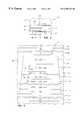
- FIG. 1is an elevation side cross-sectional view of a front portion of an exemplary magnetic head assembly employing read and write heads;
- FIG. 2is a view taken along plane 2 — 2 of FIG. 1;
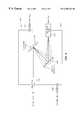
- FIG. 3is an ABS illustration of a typical tunnel junction sensor which has a barrier layer formed by the present invention
- FIG. 4is a schematic illustration of a sputtering chamber having components employed by the present invention.
- FIG. 5is a series of steps employed in the present invention.
- FIG. 6is another set of steps involved in the present invention.
- FIG. 1illustrates a cross-sectional side elevation view of the front portion of a piggyback magnetic head assembly 20 which includes a write head portion 22 and a read head portion 24 , the read head portion employing a tunnel junction sensor 26 which is partially made by the present invention.
- the tunnel junction sensor 26is located between nonmagnetic metallic first and second gap separation layers (G1) 27 and (G2) 28 and first and second gap separation layers 27 and 28 are located between ferromagnetic first and second shield layers 30 and 32 .
- the first and second shield layers 30 and 32may be employed for conducting a tunneling current T I , through the tunnel junction sensor 26 , which will be explained in more detail hereinbelow.
- the write head 22may include a ferromagnetic first pole piece layer 34 which has a yoke portion between a pole tip portion and a back gap portion.
- An insulation stack 36which may include a coil layer 38 that is embedded in first, second and third insulation layers 40 , 42 and 44 , may be located on the first pole piece layer 34 in the yoke region.
- a write gap layer 46is located on the first pole piece layer 34 in the pole tip region and may extend into the yoke region, either below or on top of the insulation stack 36 .
- a ferromagnetic second pole piece layer 48is located on the write gap layer 46 , the insulation stack 36 and is connected to the first pole piece layer 34 in the back gap region at 50 .
- an electrically insulative separation layer 52is located between the second shield layer 32 and the first pole piece layer 34 .
- the second shield layer 32 and the first pole piece layer 34are a common layer in which case the isolation layer 52 is omitted.
- the invention to be described hereinafteris applicable to either type of magnetic head assembly.
- On top of the second pole piece layer 48is an overcoat layer 54 which may be aluminum oxide.
- the magnetic head assemblyhas an air bearing surface (ABS) 56 which faces a rotating magnetic disk (not shown) for writing and reading magnetic bits to and from the disk, respectively.
- ABSair bearing surface
- FIG. 3illustrates an enlarged ABS illustration of the tunnel junction sensor 26 shown in FIGS. 1 and 2.
- the tunnel junction sensor 26includes a non-magnetic electrically insulative barrier layer 100 which is located between a ferromagnetic pinned layer (P) 102 and a ferromagnetic free layer (F) 104 .
- the pinned layer 102is located on, and exchange coupled to, an antiferromagnetic (AFM) layer 106 .
- the magnetic spins of the antiferromagnetic layer 106pin a magnetic moment 108 of the pinned layer 102 in a direction which is typically perpendicular to the ABS, as shown in FIG. 3 .
- the free layer 104has a magnetic moment 110 which is typically oriented parallel to the ABS in a quiescent state, namely when the sensor is not sensing magnetic fields from the rotating magnetic disk.
- a magnetic moment 110 of the free layerrotates upwardly and downwardly to change the resistance of the sensor to a tunneling current I T , which is conducted through the sensor perpendicular to the surface planes of the layers.
- the barrier layer 100is extremely thin which allows conduction electrons to tunnel through the barrier layer with increased or decreased resistance, depending upon whether the magnetic moment 110 is rotated toward or away from the ABS, respectively.
- a non-magnetic electrically conductive seed layer (SL) 112may be located between the antiferromagnetic pinning layer 106 and the first shield layer 30 . Furthermore, a non-magnetic electrically conductive cap 114 may be located between the free layer 104 and the second shield layer 32 . All of the layers above and below the barrier layer 100 are electrically conductive.
- the seed layer 112may make electrical contact with the first shield layer 30 and the cap layer 114 may make electrical contact with the second shield layer 32 .
- the first and second shield layers 30 and 32which are electrically conductive, may be employed as first and second leads for conducting the tunneling current I T through the tunnel junction sensor 26 .
- the barrier layer 100be ultrathin (10 ⁇ -20 ⁇ ). It is also important that the barrier layer have smooth top and bottom surfaces 116 and 118 and that the texture of the material of the barrier layer between these surfaces be uniform without defects or pinholes.
- Aluminum oxideAl 2 O 3
- the present inventionwhich will be explained hereinafter, overcomes this problem.
- Suitable thicknesses and materials of the various layers of the tunnel junction sensor 26are 20 ⁇ of tantalum (Ta) for the seed layer 112 , 150 ⁇ of platinum manganese (PtMn) for the pinning layer 106 , 30 ⁇ of cobalt iron (CoFe) for the pinned layer 102 , 10 ⁇ of aluminum oxide (Al 2 O 3 ) for the barrier layer 100 , 40 ⁇ of nickel iron (NiFe) for the free layer 104 and 50 ⁇ of tantalum (Ta) of the cap 114 .
- the first and second gap layers 27 and 28may be copper (Cu), aluminum (Al), platinum (Pt), chromium (Cr) or tantalum (Ta) with a thickness in a range of 400 ⁇ -1,000 ⁇ . It should be understood that these thicknesses and materials are exemplary. Further, either of the magnetic moments 108 and 110 may be antiparallel to that shown in FIG. 3 .
- FIG. 4schematically illustrates an exemplary sputtering chamber 200 which may be employed for practicing the present invention.
- the sputtering chamber 200includes a chamber 202 which has an inlet/outlet and valve assembly 204 for permitting drawing of a vacuum within the chamber.
- a wafer substrate 206is mounted on a fixture (not shown) within the chamber.
- a target 208is also mounted on a fixture (not shown) within the chamber.
- First and second ion beam guns 210 and 212are located within the chamber and each gun may be capable of generating a plasma and accelerating ionized gas within the chamber.
- the ion beam gun 210receives a noble gas, such as argon (Ar), krypton (Kr) or xenon (Xe), which is ionized within the gun and accelerated toward the target 208 , which is preferably aluminum (Al).
- a noble gassuch as argon (Ar), krypton (Kr) or xenon (Xe)
- the gunWhen the noble gas enters the ion beam gun 210 the gun generates a plasma which ionizes the gas and a grid in the gun accelerates the ions toward the target 208 .
- the ionsstrike the target causing aluminum atoms to be sputtered from the target 208 and deposited on the wafer substrate 206 .
- the second ion beam gun 212receives oxygen gas (O 2 ) which is ionized within the gun and disseminated into the chamber which causes ionized oxygen to envelope the wafer substrate 206 and oxidize the aluminum atoms deposited thereon to form aluminum oxide (Al 2 O 3 ).
- O 2oxygen gas
- the ion beam gun 212may have the capability of accelerating ionized oxygen toward the wafer substrate 206 it is preferred that the ionized oxygen be disseminated without acceleration. Without acceleration, energetic particle bombardment of the wafer substrate, which may deteriorate the barrier layer, is avoided.
- the ionized oxygenis accelerated toward the wafer substrate 206 by the ion beam gun 212 .
- a wafer substrate (not shown) supporting the partially completed tunnel junction sensor 26is located in the sputtering chamber 200 for formation of the aluminum oxide barrier layer 100 .
- the method of practicing the present inventionis illustrated in FIG.
- a first stepis disposing the wafer substrate 206 in the vacuum chamber 200 as shown at 300 , providing an aluminum (Al) target 208 in the chamber as shown at 302 , drawing a vacuum on the chamber via 204 as shown at 304 , directing an ion beam on the target 208 to cause aluminum atoms to be sputtered from the target and deposited on the wafer substrate 206 as shown at 306 and simultaneously with depositing the aluminum atoms on the wafer substrate, disseminating ionized oxygen in the chamber with or without acceleration that reacts with the aluminum atoms on the wafer substrate 206 to form the aluminum oxide layer on the wafer substrate as shown at 308 .
- Alaluminum
- FIG. 6Another method of the invention is shown in FIG. 6 wherein the first steps 320 and 322 are the same as the steps 300 and 302 .
- the methodincludes ionizing a noble gas in the ion beam gun 212 to produce an ionized noble gas in the chamber as shown at 324 , accelerating the ionized noble gas toward and onto the aluminum target 208 to cause the aluminum target to be sputtered and produce aluminum atoms that are deposited on the wafer substrate 206 , as shown at 326 , and simultaneously with depositing the aluminum atoms on the wafer substrate introducing oxygen gas (O 2 ) through an inlet/outlet valve assembly 327 to flood the chamber and react with the aluminum atoms on the wafer substrate to form the aluminum oxide, as shown at 328 .
- oxygen gasO 2
- the aforementioned methodsmay be employed for forming the barrier layer 100 of the tunnel junction sensor 26 shown in FIG. 3 . It should be understood, however, that the method may be employed for constructing other metal oxide layers of sensors or semiconductor devices. For instance, the method may be employed for forming the layers 28 , 52 and 46 in FIG. 1 . These layers are typically aluminum oxide (Al 2 O 3 ). It should be understood, however, that the method may be employed for forming metal oxide layers other than aluminum oxide.
- a spin valve sensormay optionally be a magnetoresistive (MR) sensor. Therefore, this invention is to be limited only by the following claims, which include all such embodiments and modifications when viewed in conjunction with the above specification and accompanying drawings.
- MRmagnetoresistive
Landscapes
- Chemical & Material Sciences (AREA)
- Chemical Kinetics & Catalysis (AREA)
- Engineering & Computer Science (AREA)
- Materials Engineering (AREA)
- Mechanical Engineering (AREA)
- Metallurgy (AREA)
- Organic Chemistry (AREA)
- Hall/Mr Elements (AREA)
- Magnetic Heads (AREA)
Abstract
Description
Claims (12)
Priority Applications (1)
| Application Number | Priority Date | Filing Date | Title |
|---|---|---|---|
| US09/344,457US6296741B1 (en) | 1999-06-25 | 1999-06-25 | Method of making oxide barrier layer for a spin tunnel junction |
Applications Claiming Priority (1)
| Application Number | Priority Date | Filing Date | Title |
|---|---|---|---|
| US09/344,457US6296741B1 (en) | 1999-06-25 | 1999-06-25 | Method of making oxide barrier layer for a spin tunnel junction |
Publications (1)
| Publication Number | Publication Date |
|---|---|
| US6296741B1true US6296741B1 (en) | 2001-10-02 |
Family
ID=23350621
Family Applications (1)
| Application Number | Title | Priority Date | Filing Date |
|---|---|---|---|
| US09/344,457Expired - Fee RelatedUS6296741B1 (en) | 1999-06-25 | 1999-06-25 | Method of making oxide barrier layer for a spin tunnel junction |
Country Status (1)
| Country | Link |
|---|---|
| US (1) | US6296741B1 (en) |
Cited By (16)
| Publication number | Priority date | Publication date | Assignee | Title |
|---|---|---|---|---|
| US20030137039A1 (en)* | 2001-11-16 | 2003-07-24 | Tdk Corporation | Packaging substrate and manufacturing method thereof, integrated circuit device and manufacturing method thereof, and saw device |
| US6655006B2 (en)* | 2001-06-28 | 2003-12-02 | International Business Machines Corporation | Method of making a tunnel junction sensor with a smooth interface between a pinned or free layer and a barrier layer |
| US20040020761A1 (en)* | 2002-05-06 | 2004-02-05 | Guardian Industries Corp. | Sputter coating apparatus including ion beam source(s), and corresponding method |
| US6730395B2 (en) | 2000-12-18 | 2004-05-04 | Seagate Technology Llc | Magnetic tunnel junction using nanoparticle monolayers and applications therefor |
| US20040095692A1 (en)* | 2002-11-18 | 2004-05-20 | International Business Machines Corporation | Enhanced spin-valve sensor with engineered overlayer |
| US6831816B2 (en) | 2002-07-15 | 2004-12-14 | International Business Machines Corporation | CPP sensor with in-stack biased free layer |
| US20060057304A1 (en)* | 2002-03-16 | 2006-03-16 | Symmorphix, Inc. | Biased pulse DC reactive sputtering of oxide films |
| US20060291105A1 (en)* | 2005-06-28 | 2006-12-28 | Chang Y A | Fabrication of magnetic tunnel junctions with epitaxial and textured ferromagnetic layers |
| US20070196984A1 (en)* | 2006-02-22 | 2007-08-23 | Samsung Electronics Co., Ltd. | Nonvolatile memory device, layer deposition apparatus and method of fabricating a nonvolatile memory device using the same |
| US20080152834A1 (en)* | 2006-12-22 | 2008-06-26 | Hitachi Global Storage Technologies | Method for manufacturing a tunnel junction magnetic sensor using ion beam deposition |
| US20080210544A1 (en)* | 2006-12-22 | 2008-09-04 | Mustafa Michael Pinarbasi | Method for manufacturing a magnetic tunnel junction sensor using ion beam deposition |
| US7579042B2 (en) | 2004-07-29 | 2009-08-25 | Wisconsin Alumni Research Foundation | Methods for the fabrication of thermally stable magnetic tunnel junctions |
| US8365393B1 (en)* | 2005-07-08 | 2013-02-05 | Seagate Technology Llc | Manufacturing methods for write heads with floating side shields |
| US8636876B2 (en) | 2004-12-08 | 2014-01-28 | R. Ernest Demaray | Deposition of LiCoO2 |
| US8728285B2 (en) | 2003-05-23 | 2014-05-20 | Demaray, Llc | Transparent conductive oxides |
| US10319817B2 (en) | 2017-09-11 | 2019-06-11 | International Business Machines Corporation | Lattice matched epitaxial oxide layer for a super steep retrograde well |
Citations (10)
| Publication number | Priority date | Publication date | Assignee | Title |
|---|---|---|---|---|
| US4920094A (en)* | 1987-03-27 | 1990-04-24 | Nissin Electric Co., Ltd. | Process for producing superconducting thin films |
| US4923585A (en)* | 1988-11-02 | 1990-05-08 | Arch Development Corporation | Sputter deposition for multi-component thin films |
| US4994164A (en)* | 1987-08-05 | 1991-02-19 | U.S. Philips Corporation | Metal ion implantation apparatus |
| US5454919A (en)* | 1992-12-03 | 1995-10-03 | Gec-Marconi Avionics Holdings Limited | Depositing different materials on a substrate |
| US5650958A (en)* | 1996-03-18 | 1997-07-22 | International Business Machines Corporation | Magnetic tunnel junctions with controlled magnetic response |
| US5750275A (en)* | 1996-07-12 | 1998-05-12 | Read-Rite Corporation | Thin film heads with insulated laminations for improved high frequency performance |
| US5768065A (en)* | 1992-01-28 | 1998-06-16 | Tdk Corporation | Thin film magnetic head |
| US5768071A (en)* | 1997-06-19 | 1998-06-16 | International Business Machines Corporation | Spin valve sensor with improved magnetic stability of the pinned layer |
| US5898547A (en)* | 1997-10-24 | 1999-04-27 | International Business Machines Corporation | Magnetic tunnel junction magnetoresistive read head with sensing layer as flux guide |
| US5962080A (en)* | 1995-04-17 | 1999-10-05 | Read-Rite Corporation | Deposition of insulating thin film by a plurality of ion beams |
- 1999
- 1999-06-25USUS09/344,457patent/US6296741B1/ennot_activeExpired - Fee Related
Patent Citations (10)
| Publication number | Priority date | Publication date | Assignee | Title |
|---|---|---|---|---|
| US4920094A (en)* | 1987-03-27 | 1990-04-24 | Nissin Electric Co., Ltd. | Process for producing superconducting thin films |
| US4994164A (en)* | 1987-08-05 | 1991-02-19 | U.S. Philips Corporation | Metal ion implantation apparatus |
| US4923585A (en)* | 1988-11-02 | 1990-05-08 | Arch Development Corporation | Sputter deposition for multi-component thin films |
| US5768065A (en)* | 1992-01-28 | 1998-06-16 | Tdk Corporation | Thin film magnetic head |
| US5454919A (en)* | 1992-12-03 | 1995-10-03 | Gec-Marconi Avionics Holdings Limited | Depositing different materials on a substrate |
| US5962080A (en)* | 1995-04-17 | 1999-10-05 | Read-Rite Corporation | Deposition of insulating thin film by a plurality of ion beams |
| US5650958A (en)* | 1996-03-18 | 1997-07-22 | International Business Machines Corporation | Magnetic tunnel junctions with controlled magnetic response |
| US5750275A (en)* | 1996-07-12 | 1998-05-12 | Read-Rite Corporation | Thin film heads with insulated laminations for improved high frequency performance |
| US5768071A (en)* | 1997-06-19 | 1998-06-16 | International Business Machines Corporation | Spin valve sensor with improved magnetic stability of the pinned layer |
| US5898547A (en)* | 1997-10-24 | 1999-04-27 | International Business Machines Corporation | Magnetic tunnel junction magnetoresistive read head with sensing layer as flux guide |
Cited By (23)
| Publication number | Priority date | Publication date | Assignee | Title |
|---|---|---|---|---|
| US6730395B2 (en) | 2000-12-18 | 2004-05-04 | Seagate Technology Llc | Magnetic tunnel junction using nanoparticle monolayers and applications therefor |
| US6655006B2 (en)* | 2001-06-28 | 2003-12-02 | International Business Machines Corporation | Method of making a tunnel junction sensor with a smooth interface between a pinned or free layer and a barrier layer |
| US6891704B2 (en) | 2001-06-28 | 2005-05-10 | International Business Machines Corporation | Tunnel junction sensor with a smooth interface between a pinned or free layer and a barrier layer |
| US20030137039A1 (en)* | 2001-11-16 | 2003-07-24 | Tdk Corporation | Packaging substrate and manufacturing method thereof, integrated circuit device and manufacturing method thereof, and saw device |
| US20060057304A1 (en)* | 2002-03-16 | 2006-03-16 | Symmorphix, Inc. | Biased pulse DC reactive sputtering of oxide films |
| US8105466B2 (en) | 2002-03-16 | 2012-01-31 | Springworks, Llc | Biased pulse DC reactive sputtering of oxide films |
| US20040020761A1 (en)* | 2002-05-06 | 2004-02-05 | Guardian Industries Corp. | Sputter coating apparatus including ion beam source(s), and corresponding method |
| US7198699B2 (en) | 2002-05-06 | 2007-04-03 | Guardian Industries Corp. | Sputter coating apparatus including ion beam source(s), and corresponding method |
| US6831816B2 (en) | 2002-07-15 | 2004-12-14 | International Business Machines Corporation | CPP sensor with in-stack biased free layer |
| US7007373B2 (en) | 2002-11-18 | 2006-03-07 | Hitachi Global Storage Technologies Netherlands B.V. | Method of manufacturing enhanced spin-valve sensor with engineered overlayer |
| US7352542B2 (en) | 2002-11-18 | 2008-04-01 | Hitachi Global Storage Technologies Netherlands B.V | Enhanced spin-valve sensor with engineered overlayer formed on a free layer |
| US20040095692A1 (en)* | 2002-11-18 | 2004-05-20 | International Business Machines Corporation | Enhanced spin-valve sensor with engineered overlayer |
| US8728285B2 (en) | 2003-05-23 | 2014-05-20 | Demaray, Llc | Transparent conductive oxides |
| US7579042B2 (en) | 2004-07-29 | 2009-08-25 | Wisconsin Alumni Research Foundation | Methods for the fabrication of thermally stable magnetic tunnel junctions |
| US8636876B2 (en) | 2004-12-08 | 2014-01-28 | R. Ernest Demaray | Deposition of LiCoO2 |
| US7450352B2 (en) | 2005-06-28 | 2008-11-11 | Wisconsin Alumni Research Foundation | Fabrication of magnetic tunnel junctions with epitaxial and textured ferromagnetic layers |
| US20060291105A1 (en)* | 2005-06-28 | 2006-12-28 | Chang Y A | Fabrication of magnetic tunnel junctions with epitaxial and textured ferromagnetic layers |
| US8365393B1 (en)* | 2005-07-08 | 2013-02-05 | Seagate Technology Llc | Manufacturing methods for write heads with floating side shields |
| US8995086B2 (en) | 2005-07-08 | 2015-03-31 | Seagate Technology Llc | Write head with floating side shields and enhanced magnetic potential |
| US20070196984A1 (en)* | 2006-02-22 | 2007-08-23 | Samsung Electronics Co., Ltd. | Nonvolatile memory device, layer deposition apparatus and method of fabricating a nonvolatile memory device using the same |
| US20080210544A1 (en)* | 2006-12-22 | 2008-09-04 | Mustafa Michael Pinarbasi | Method for manufacturing a magnetic tunnel junction sensor using ion beam deposition |
| US20080152834A1 (en)* | 2006-12-22 | 2008-06-26 | Hitachi Global Storage Technologies | Method for manufacturing a tunnel junction magnetic sensor using ion beam deposition |
| US10319817B2 (en) | 2017-09-11 | 2019-06-11 | International Business Machines Corporation | Lattice matched epitaxial oxide layer for a super steep retrograde well |
Similar Documents
| Publication | Publication Date | Title |
|---|---|---|
| US6296741B1 (en) | Method of making oxide barrier layer for a spin tunnel junction | |
| US6800565B2 (en) | Method of forming thin oxidation layer by cluster ion beam | |
| US6482657B2 (en) | Methods of manufacturing tunnel magnetoresistive element, thin-film magnetic head and memory element | |
| US6434814B1 (en) | Method of manufacturing a magnetic head including a read head with read track width defining layer that planarizes the write gap layer of a write head | |
| US7920363B2 (en) | TMR sensor having magnesium/magnesium oxide tunnel barrier | |
| US5514477A (en) | Corrosion-resistant laminate which consists of a metal of a single mass number deposited on a substrate | |
| US6891704B2 (en) | Tunnel junction sensor with a smooth interface between a pinned or free layer and a barrier layer | |
| US20030087130A1 (en) | Magnetoresistive sensor and manufacturing method therefor | |
| JP2002076473A (en) | Magnetoresistive element, method and apparatus for manufacturing the same, and magnetic reproducing apparatus | |
| US6783635B2 (en) | Spin valve sensor free layer structure with a cobalt based layer that promotes magnetic stability and high magnetoresistance | |
| US20080152834A1 (en) | Method for manufacturing a tunnel junction magnetic sensor using ion beam deposition | |
| US6306266B1 (en) | Method of making a top spin valve sensor with an in-situ formed seed layer structure for improving sensor performance | |
| US7038890B2 (en) | Current perpendicular to the planes (CPP) sensor with a highly conductive cap structure | |
| US20080316656A1 (en) | Magnetic head and method of manufacturing the magnetic head | |
| US6398924B1 (en) | Spin valve sensor with improved pinning field between nickel oxide (NiO) pinning layer and pinned layer | |
| US6226158B1 (en) | High operating temperature gold leads for a read sensor | |
| KR101977795B1 (en) | Methods of forming mgo barrier layer | |
| KR100376744B1 (en) | METHOD OF MAKING LOW STRESS AND LOW RESISTANCE RHODIUM(Rh) LEADS | |
| US6428657B1 (en) | Magnetic read head sensor with a reactively sputtered pinning layer structure | |
| US6820322B2 (en) | Method of making a spin valve sensor with a free layer structure sputter deposited in a nitrogen atmosphere | |
| US7676904B2 (en) | Method of manufacturing high sensitivity spin valve designs with ion beam treatment | |
| US7088561B2 (en) | Method of making a tunnel valve sensor with improved free layer sensitivity | |
| US20080210544A1 (en) | Method for manufacturing a magnetic tunnel junction sensor using ion beam deposition | |
| US7097745B2 (en) | Method of forming a tunneling magnetoresistive head | |
| US6787004B2 (en) | Method for manufacturing a spin valve film and a method of manufacturing a magnetoresistance-effect type magnetic head |
Legal Events
| Date | Code | Title | Description |
|---|---|---|---|
| AS | Assignment | Owner name:INTERNATIONAL BUSINESS MACHINES CORPORATION, NEW Y Free format text:ASSIGNMENT OF ASSIGNORS INTEREST;ASSIGNOR:PINARBASI, MUSTAFA;REEL/FRAME:010071/0072 Effective date:19990623 | |
| AS | Assignment | Owner name:HITACHI GLOBAL STORAGE TECHNOLOGIES NETHERLANDS B. Free format text:CHANGE OF NAME;ASSIGNOR:MARIANA HDD B.V.;REEL/FRAME:014871/0450 Effective date:20021231 Owner name:MARIANA HDD B.V., NETHERLANDS Free format text:ASSIGNMENT OF ASSIGNORS INTEREST;ASSIGNOR:INTERNATIONAL BUSINESS MACHINES CORPORATION;REEL/FRAME:014871/0746 Effective date:20021231 | |
| FEPP | Fee payment procedure | Free format text:PAYOR NUMBER ASSIGNED (ORIGINAL EVENT CODE: ASPN); ENTITY STATUS OF PATENT OWNER: LARGE ENTITY | |
| FPAY | Fee payment | Year of fee payment:4 | |
| REMI | Maintenance fee reminder mailed | ||
| LAPS | Lapse for failure to pay maintenance fees | ||
| STCH | Information on status: patent discontinuation | Free format text:PATENT EXPIRED DUE TO NONPAYMENT OF MAINTENANCE FEES UNDER 37 CFR 1.362 | |
| FP | Lapsed due to failure to pay maintenance fee | Effective date:20091002 |