US6296740B1 - Pretreatment process for a surface texturing process - Google Patents
Pretreatment process for a surface texturing processDownload PDFInfo
- Publication number
- US6296740B1 US6296740B1US08/427,462US42746295AUS6296740B1US 6296740 B1US6296740 B1US 6296740B1US 42746295 AUS42746295 AUS 42746295AUS 6296740 B1US6296740 B1US 6296740B1
- Authority
- US
- United States
- Prior art keywords
- substrate
- micro
- tips
- sample
- layer
- Prior art date
- Legal status (The legal status is an assumption and is not a legal conclusion. Google has not performed a legal analysis and makes no representation as to the accuracy of the status listed.)
- Expired - Fee Related
Links
- 238000000034methodMethods0.000titleclaimsabstractdescription52
- 239000000463materialSubstances0.000claimsabstractdescription68
- 238000005498polishingMethods0.000claimsabstractdescription16
- 239000000758substrateSubstances0.000claimsabstractdescription16
- 238000005530etchingMethods0.000claimsabstractdescription12
- 229910003460diamondInorganic materials0.000claimsabstractdescription7
- 239000010432diamondSubstances0.000claimsabstractdescription7
- 238000005488sandblastingMethods0.000claimsabstractdescription5
- 238000000151depositionMethods0.000claimsdescription12
- 238000004519manufacturing processMethods0.000claimsdescription7
- 238000004544sputter depositionMethods0.000claimsdescription7
- 239000007921spraySubstances0.000claimsdescription6
- 239000000443aerosolSubstances0.000claimsdescription3
- PNEYBMLMFCGWSK-UHFFFAOYSA-Naluminium oxideInorganic materials[O-2].[O-2].[O-2].[Al+3].[Al+3]PNEYBMLMFCGWSK-UHFFFAOYSA-N0.000claimsdescription3
- 229910052593corundumInorganic materials0.000claimsdescription2
- 229910001845yogo sapphireInorganic materials0.000claimsdescription2
- 230000015572biosynthetic processEffects0.000abstractdescription8
- 238000000206photolithographyMethods0.000abstractdescription5
- 238000006748scratchingMethods0.000abstractdescription3
- 230000002393scratching effectEffects0.000abstractdescription3
- 238000000992sputter etchingMethods0.000abstractdescription3
- 238000010884ion-beam techniqueMethods0.000description14
- ZOKXTWBITQBERF-UHFFFAOYSA-NMolybdenumChemical compound[Mo]ZOKXTWBITQBERF-UHFFFAOYSA-N0.000description7
- 239000010949copperSubstances0.000description7
- 230000009977dual effectEffects0.000description7
- 229910052750molybdenumInorganic materials0.000description7
- 239000011733molybdenumSubstances0.000description7
- VYZAMTAEIAYCRO-UHFFFAOYSA-NChromiumChemical compound[Cr]VYZAMTAEIAYCRO-UHFFFAOYSA-N0.000description6
- 230000007547defectEffects0.000description6
- 230000008021depositionEffects0.000description6
- 239000011521glassSubstances0.000description5
- 239000011651chromiumSubstances0.000description4
- 238000001659ion-beam spectroscopyMethods0.000description4
- 229910052751metalInorganic materials0.000description4
- 239000002184metalSubstances0.000description4
- RYGMFSIKBFXOCR-UHFFFAOYSA-NCopperChemical compound[Cu]RYGMFSIKBFXOCR-UHFFFAOYSA-N0.000description3
- KFZMGEQAYNKOFK-UHFFFAOYSA-NIsopropanolChemical compoundCC(C)OKFZMGEQAYNKOFK-UHFFFAOYSA-N0.000description3
- 229910021417amorphous siliconInorganic materials0.000description3
- 229910052804chromiumInorganic materials0.000description3
- 229910052802copperInorganic materials0.000description3
- 239000002245particleSubstances0.000description3
- 238000007517polishing processMethods0.000description3
- 229920006395saturated elastomerPolymers0.000description3
- XUIMIQQOPSSXEZ-UHFFFAOYSA-NSiliconChemical compound[Si]XUIMIQQOPSSXEZ-UHFFFAOYSA-N0.000description2
- 238000005229chemical vapour depositionMethods0.000description2
- 238000005566electron beam evaporationMethods0.000description2
- 238000005516engineering processMethods0.000description2
- 238000001552radio frequency sputter depositionMethods0.000description2
- 238000000926separation methodMethods0.000description2
- 229910052710siliconInorganic materials0.000description2
- 239000010703siliconSubstances0.000description2
- 239000002002slurrySubstances0.000description2
- 239000010936titaniumSubstances0.000description2
- 229910001868waterInorganic materials0.000description2
- 235000010627Phaseolus vulgarisNutrition0.000description1
- 244000046052Phaseolus vulgarisSpecies0.000description1
- BQCADISMDOOEFD-UHFFFAOYSA-NSilverChemical compound[Ag]BQCADISMDOOEFD-UHFFFAOYSA-N0.000description1
- RTAQQCXQSZGOHL-UHFFFAOYSA-NTitaniumChemical compound[Ti]RTAQQCXQSZGOHL-UHFFFAOYSA-N0.000description1
- 230000004075alterationEffects0.000description1
- 239000008367deionised waterSubstances0.000description1
- 229910021641deionized waterInorganic materials0.000description1
- 230000001419dependent effectEffects0.000description1
- 238000010586diagramMethods0.000description1
- 238000001017electron-beam sputter depositionMethods0.000description1
- 239000012530fluidSubstances0.000description1
- 238000010849ion bombardmentMethods0.000description1
- 238000002203pretreatmentMethods0.000description1
- 239000004576sandSubstances0.000description1
- 229910052709silverInorganic materials0.000description1
- 239000004332silverSubstances0.000description1
- 238000006467substitution reactionMethods0.000description1
- 229910052719titaniumInorganic materials0.000description1
- WFKWXMTUELFFGS-UHFFFAOYSA-NtungstenChemical compound[W]WFKWXMTUELFFGS-UHFFFAOYSA-N0.000description1
- 229910052721tungstenInorganic materials0.000description1
- 239000010937tungstenSubstances0.000description1
- XLYOFNOQVPJJNP-UHFFFAOYSA-NwaterChemical compoundOXLYOFNOQVPJJNP-UHFFFAOYSA-N0.000description1
Images


Classifications
- C—CHEMISTRY; METALLURGY
- C23—COATING METALLIC MATERIAL; COATING MATERIAL WITH METALLIC MATERIAL; CHEMICAL SURFACE TREATMENT; DIFFUSION TREATMENT OF METALLIC MATERIAL; COATING BY VACUUM EVAPORATION, BY SPUTTERING, BY ION IMPLANTATION OR BY CHEMICAL VAPOUR DEPOSITION, IN GENERAL; INHIBITING CORROSION OF METALLIC MATERIAL OR INCRUSTATION IN GENERAL
- C23C—COATING METALLIC MATERIAL; COATING MATERIAL WITH METALLIC MATERIAL; SURFACE TREATMENT OF METALLIC MATERIAL BY DIFFUSION INTO THE SURFACE, BY CHEMICAL CONVERSION OR SUBSTITUTION; COATING BY VACUUM EVAPORATION, BY SPUTTERING, BY ION IMPLANTATION OR BY CHEMICAL VAPOUR DEPOSITION, IN GENERAL
- C23C14/00—Coating by vacuum evaporation, by sputtering or by ion implantation of the coating forming material
- C23C14/22—Coating by vacuum evaporation, by sputtering or by ion implantation of the coating forming material characterised by the process of coating
- C—CHEMISTRY; METALLURGY
- C23—COATING METALLIC MATERIAL; COATING MATERIAL WITH METALLIC MATERIAL; CHEMICAL SURFACE TREATMENT; DIFFUSION TREATMENT OF METALLIC MATERIAL; COATING BY VACUUM EVAPORATION, BY SPUTTERING, BY ION IMPLANTATION OR BY CHEMICAL VAPOUR DEPOSITION, IN GENERAL; INHIBITING CORROSION OF METALLIC MATERIAL OR INCRUSTATION IN GENERAL
- C23C—COATING METALLIC MATERIAL; COATING MATERIAL WITH METALLIC MATERIAL; SURFACE TREATMENT OF METALLIC MATERIAL BY DIFFUSION INTO THE SURFACE, BY CHEMICAL CONVERSION OR SUBSTITUTION; COATING BY VACUUM EVAPORATION, BY SPUTTERING, BY ION IMPLANTATION OR BY CHEMICAL VAPOUR DEPOSITION, IN GENERAL
- C23C14/00—Coating by vacuum evaporation, by sputtering or by ion implantation of the coating forming material
- C23C14/02—Pretreatment of the material to be coated
- C23C14/028—Physical treatment to alter the texture of the substrate surface, e.g. grinding, polishing
Definitions
- the present inventionrelates in general to a surface texturing process, and more particularly, to a pretreatment process performed prior to performing a surface texturing process wherein irregularities are produced on a surface to be textured using an ion beam.
- a cone (micro-tip) structuremay be produced by using an ion source for etching a material, such as copper, after it has been seeded with a second material, such as molybdenum.
- a dual ion beam systemis utilized to efficiently control the ion beam sputtering process.
- the surface textured structurebe uniform in terms of the density, height and shape of the resultant cones. Additionally, for mass production manufacturing, the process should be controllable and repeatable. However, the above-noted surface texturing process using ion beam sources is difficult to control, and the structures of the cones are not as uniform as many applications require, such as for flat panel display devices.
- micro-tipand “cone” are used interchangeably
- a material layeris deposited upon a substrate.
- An irregularityis then formed in the surface of the material prior to loading the sample into an evacuated chamber to be subject to an ion milling process.
- the ion milling processsputters a seed material onto the surface of the material.
- An ion beamis then utilized to etch the material, resulting in cones or micro-tips being formed thereon.
- the irregularitiesare nuclei sites for collecting the seed material.
- An irregularitymay be formed by polishing the surface with a polishing solution, such as a diamond spray.
- an irregularitymay be formed by bombarding the surface through a sandblasting technique.
- an irregularitymay be formed using a photolithography technique, whereby a step feature is caused to be formed on the surface of the material.
- an irregularitymay be formed through a mechanical means, such as by scratching the surface with a needle.
- a dual ion beam systemis utilized whereby one ion beam source is used to sputter the seed material onto the surface of the material, while a second ion beam source is utilized for the etching portion of the process.
- the material upon which the irregularities are formedis an emitter material that may be utilized in a field emission device, wherein electrons are emitted from the formed micro-tips under the influence of a potential field.
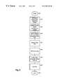
- FIG. 1illustrates a dual ion beam system for producing micro-tip structures
- FIGS. 2 and 3illustrate a formation of micro-tips
- FIG. 4illustrates a preferred embodiment of the present invention
- FIG. 5illustrates an alternative embodiment of the present invention utilizing a polishing technique
- FIG. 6illustrates an alternative embodiment of the present invention utilizing a sandblasting technique
- FIGS. 7A-7Billustrate an alternative embodiment of the present invention utilizing a photolithography technique
- FIG. 8illustrates an alternative embodiment of the present invention using mechanical means for creating defects in the surface of a sample
- FIG. 9illustrates a sample having had dints produced thereon.
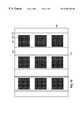
- FIG. 10illustrates a top view of an apparatus fabricated in accordance with the present invention.
- FIG. 1there is illustrated dual ion beam system 10 in accordance with the cross-referenced patent application Ser. No. 08/427,462, now U.S. Pat. No. 5,628,659.
- the ion beams produced by Kaufman ion source 13are utilized to etch material 304
- Kaufman ion source 12is utilized to sputter seed material onto material 304 .
- Evacuated chamber 15(alternatively chamber 15 may be filled with a particular gas) may be utilized to enclose system 10 .
- glass substrate 308is first cleaned. Next, depending upon the particular structure desired, a layer of 700 angstroms of chromium (Cr) is optionally deposited upon glass substrate 308 .
- layer 305is deposited using electron beam evaporation, sputtering or a CVD (chemical vapor deposition) process.
- Layer 305may be a resistive layer of 5,000 angstroms (0.5 ⁇ m) of amorphous silicon (a-Si).
- a 3 ⁇ m (micrometer) copper (Cu) film layer 304is deposited upon layer 305 , preferably utilizing electron beam evaporation.
- This entire structurewhich may eventually comprise the cathode of a flat panel display is then loaded into system 10 and coupled to heater 11 . Since the formation of the cones, or micro-tips, is a temperature-dependent process heater 11 is used to assist in controlling the entire process.
- Ion source 13is utilized to etch away portions of material 304 , ion source 12 is utilized to sputter a seed material, which is preferably molybdenum (Mo), onto material 304 .
- Ion source 13is preferably operated with a beam energy of 800 volts and a beam current of 80 milliamps, while ion source 12 is preferably operated with a beam energy of 800 volts and a beam current of 50 milliamps.
- the molybdenum seed materialis sputtered onto material 304 by the bombardment of molybdenum target 14 with an ion beam from ion source 12 .
- Ion beam source 13etches away material 304 while ion beam source 12 sputters a seed material from target 14 to deposit on the surface of material 304 .
- source 12 and target 14can be replaced with other deposition equipment, such as RF sputtering.
- the structure, density and height of tips 304are sensitive to the ratio of the etching rate and the deposition rate of the seed material.
- the etching rate for Cuis 8 angstroms per second and the deposition rate for Mo is 0.2 angstroms per second. These conditions are achieved at the above noted 800 volts beam voltage and 50 milliamp beam current for source 12 , and 80 milliamp beam current for source 13 .
- Very small amounts of seed materialcan give rise to seed cone formation in material 304 .
- the ratio of Mo atoms arriving at material 304can be as low as one seed atom per 500 sputtered Cu target atoms. In other words, the ratio of the deposition rate to the etching rate can be as low as 1/500.
- Control of this processis implemented with the assistance of mass spectrometer 16 , which is utilized to monitor the etching process.
- mass spectrometer 16detects a preselected amount of material 305 , the etching process may be terminated. For example, if material 305 is amorphous silicon, then mass spectrometer 16 will monitor for a preselected amount of silicon. If a preselected amount of silicon is monitored, then the process may be terminated either manually or automatically.
- material 304may also be comprised of Titanium (Ti) or silver (Ag), while molybdenum may be replaced by tungsten (W).
- irregularities in the surface of layer 304may be produced. It has been found that cones 304 such as those illustrated in FIG. 3 are more likely to grow in an area where the surface of layer 304 has been “damaged” in some way. The following describes various alternative methods of “damaging” the surface of layer 304 .
- sample 53the sample comprising glass substrate 308 with layer 304 will also be referred to as sample 53 .
- layer 305is optional.
- step 401there is illustrated a process for polishing the surface of layer 304 with a LECO® Aerosol Diamond Spray before submitting sample 53 for ion bombardment within system 10 .
- the diamond particles within the sprayare 0.25 ⁇ m in diameter.
- the processbegins at step 401 and proceeds to step 402 , wherein a fresh TX172 TEXWIPE® swab is saturated when the LECO® 0.25 ⁇ m aerosol diamond spray.
- step 403sample 53 is laid face up on a clean lint-free tissue and swiped lightly from left to right approximately 46 times with the saturated swab. The fluid is then allowed to evaporate from the surface of layer 304 .
- step 404a fresh TX172 TEXWIPE® swab is saturated with isopropyl alcohol (“IPA”), which is utilized to swipe the sample from left to right approximately 25 times.
- step 405the surface of layer 304 is then rinsed with IPA twice.
- step 406the surface is dried with dry N 2 .
- step 407sample 53 is then loaded into dual ion bean system 10 for the ion beam sputtering process described above. Using this process, the uniformity of the cone structures (including height, shape and density) is improved. This process also results in an ability to produce the cones in a more controllable and repeatable manner.
- the diamond spray solutionmay be replaced with a different polishing solution comprised of 50 nm Al2O3+DI-H2O (deionized water).
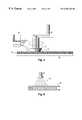
- sample 53is mounted to sample holder 52 , which is a portion of polishing machine 50 , which may be a Model 372 polisher made by Westech Systems, Inc. As noted by the arrows in FIG. 5, polishing machine 50 has an ability to slide and rotate sample 53 across the surface of polishing pad 54 , which is a Rodel 750 finishing pad, which is mounted upon flat surface 55 . Sample 53 may be rotated at 50 rpm. The contact pressure between pad 54 and sample 53 is preferably 1 psi (pound per square inch). The sample is preferably polished for 30 seconds.
- a polishingmay be contained within container 51 is poured onto the surface of polishing pad 54 .
- FIG. 6there is illustrated another alternative embodiment of the present invention, which utilizes a sandblasting process to create the defects on the surface of layer 304 before subjecting sample 53 to the process of system 10 .
- Sandblaster 60(Trinco Dry Blast, Model 48/EF2) is utilized to blast the surface of layer 304 with sand particles 61 at approximately an air pressure of 15 psi. 90% of particles 61 are in the range of 148 ⁇ m-188 ⁇ m in diameter.
- the distance between nozzle 60 and sample 53is preferably 15 inches.
- Surface finishing timeis approximately one minute.
- FIGS. 7A and 7Bthere is illustrated another alternative embodiment of the present invention, wherein photolithography techniques are utilized to create a minute “step” on the surface of layer 304 .
- the conesare then grown along the edges of these created steps. With such a process, there is an ability to selectively grow the cones or micro-tips exactly where they are desired.
- the first portion of this processis a deposition of a 700 angstrom layer of chromium 700 or an equivalent material on the clean surface of glass substrate 308 , utilizing a sputtering technology along with photolithography in order to pattern film layer 700 into 50 ⁇ m wide strips having a separation therebetween of 50 ⁇ m. Of course, other width strips and separations may be utilized.
- a 3 ⁇ m copper film 304 or an equivalent materialis deposited on top of glass substrate 308 with chromium strips 700 utilizing a sputtering technique.
- the result of this processis “steps” 701 and 702 on the surface of layer 304 .
- the edges of the “steps” 701 , 702are the imperfections upon which the cones are to be grown.
- the entire sample 70is then mounted in system 10 for the dual ion beam sputtering surface texturing process, which produces cones 304 as illustrated in FIG. 7 B.
- FIG. 8there is shown yet another alternative embodiment of the present invention wherein defects on the surface of layer 304 are produced by mechanical means such as by scratching the surface of layer 304 using a fine needle 80 . Cones are then grown along the edges of the scratches.
- the present inventionresults in cones grown near or at defects or irregularities on the surface of material 304 .
- the aforementioned polishing processescreate defects on the surface by creating a number of small dints 90 as illustrated in FIG. 9 .
- the surface of material 304 previous to producing any type of irregularity to any of the aforementioned techniquesis quite smooth and damage-free as a result of the deposition of layer 304 by RF sputtering.
- the irregularitiesare the nuclei sites for cone growth because the seed material (in this case molybdenum sputtered onto surface 304 by system 10 ) is likely trapped inside or adjacent to the irregularities.
- pretreatmentse.g., polishing, steps, sandblast, etc. create many preferable sites for seed atoms to form clusters, which are the nuclei sites for cone growth.
Landscapes
- Chemical & Material Sciences (AREA)
- Chemical Kinetics & Catalysis (AREA)
- Engineering & Computer Science (AREA)
- Materials Engineering (AREA)
- Mechanical Engineering (AREA)
- Metallurgy (AREA)
- Organic Chemistry (AREA)
- Physical Vapour Deposition (AREA)
Abstract
Description
Claims (5)
Priority Applications (2)
| Application Number | Priority Date | Filing Date | Title |
|---|---|---|---|
| US08/427,462US6296740B1 (en) | 1995-04-24 | 1995-04-24 | Pretreatment process for a surface texturing process |
| US09/778,430US6613204B2 (en) | 1995-04-24 | 2001-02-07 | Pretreatment process for a surface texturing process |
Applications Claiming Priority (1)
| Application Number | Priority Date | Filing Date | Title |
|---|---|---|---|
| US08/427,462US6296740B1 (en) | 1995-04-24 | 1995-04-24 | Pretreatment process for a surface texturing process |
Related Child Applications (1)
| Application Number | Title | Priority Date | Filing Date |
|---|---|---|---|
| US09/778,430DivisionUS6613204B2 (en) | 1995-04-24 | 2001-02-07 | Pretreatment process for a surface texturing process |
Publications (1)
| Publication Number | Publication Date |
|---|---|
| US6296740B1true US6296740B1 (en) | 2001-10-02 |
Family
ID=23694978
Family Applications (2)
| Application Number | Title | Priority Date | Filing Date |
|---|---|---|---|
| US08/427,462Expired - Fee RelatedUS6296740B1 (en) | 1995-04-24 | 1995-04-24 | Pretreatment process for a surface texturing process |
| US09/778,430Expired - Fee RelatedUS6613204B2 (en) | 1995-04-24 | 2001-02-07 | Pretreatment process for a surface texturing process |
Family Applications After (1)
| Application Number | Title | Priority Date | Filing Date |
|---|---|---|---|
| US09/778,430Expired - Fee RelatedUS6613204B2 (en) | 1995-04-24 | 2001-02-07 | Pretreatment process for a surface texturing process |
Country Status (1)
| Country | Link |
|---|---|
| US (2) | US6296740B1 (en) |
Cited By (18)
| Publication number | Priority date | Publication date | Assignee | Title |
|---|---|---|---|---|
| US20040063333A1 (en)* | 2002-09-30 | 2004-04-01 | Tokyo Electron Limited | Method and apparatus for an improved baffle plate in a plasma processing system |
| US20040081746A1 (en)* | 2000-12-12 | 2004-04-29 | Kosuke Imafuku | Method for regenerating container for plasma treatment, member inside container for plasma treatment, method for preparing member inside container for plasma treatment, and apparatus for plasma treatment |
| US6761803B2 (en)* | 2001-12-17 | 2004-07-13 | City University Of Hong Kong | Large area silicon cone arrays fabrication and cone based nanostructure modification |
| US20050136788A1 (en)* | 2003-12-18 | 2005-06-23 | Nano-Proprietary, Inc. | Bead blast activation of carbon nanotube cathode |
| US7137353B2 (en) | 2002-09-30 | 2006-11-21 | Tokyo Electron Limited | Method and apparatus for an improved deposition shield in a plasma processing system |
| US7147749B2 (en) | 2002-09-30 | 2006-12-12 | Tokyo Electron Limited | Method and apparatus for an improved upper electrode plate with deposition shield in a plasma processing system |
| US7163585B2 (en) | 2002-09-30 | 2007-01-16 | Tokyo Electron Limited | Method and apparatus for an improved optical window deposition shield in a plasma processing system |
| US7166200B2 (en) | 2002-09-30 | 2007-01-23 | Tokyo Electron Limited | Method and apparatus for an improved upper electrode plate in a plasma processing system |
| US7204912B2 (en) | 2002-09-30 | 2007-04-17 | Tokyo Electron Limited | Method and apparatus for an improved bellows shield in a plasma processing system |
| US7282112B2 (en) | 2002-09-30 | 2007-10-16 | Tokyo Electron Limited | Method and apparatus for an improved baffle plate in a plasma processing system |
| US7291566B2 (en) | 2003-03-31 | 2007-11-06 | Tokyo Electron Limited | Barrier layer for a processing element and a method of forming the same |
| US20070278925A1 (en)* | 2004-09-10 | 2007-12-06 | Nano-Proprietary, Inc. | Enhanced electron field emission from carbon nanotubes without activation |
| US7552521B2 (en) | 2004-12-08 | 2009-06-30 | Tokyo Electron Limited | Method and apparatus for improved baffle plate |
| US7560376B2 (en) | 2003-03-31 | 2009-07-14 | Tokyo Electron Limited | Method for adjoining adjacent coatings on a processing element |
| US7601242B2 (en) | 2005-01-11 | 2009-10-13 | Tokyo Electron Limited | Plasma processing system and baffle assembly for use in plasma processing system |
| US7780786B2 (en) | 2002-11-28 | 2010-08-24 | Tokyo Electron Limited | Internal member of a plasma processing vessel |
| US7846291B2 (en) | 1999-12-10 | 2010-12-07 | Tokyo Electron Limited | Processing apparatus with a chamber having therein a high-corrosion-resistant sprayed film |
| CN114102272A (en)* | 2021-12-03 | 2022-03-01 | 湖北久之洋红外系统股份有限公司 | Ion beam polishing method for high-precision C-direction sapphire window |
Families Citing this family (8)
| Publication number | Priority date | Publication date | Assignee | Title |
|---|---|---|---|---|
| KR100279051B1 (en)* | 1997-09-23 | 2001-02-01 | 박호군 | Manufacturing method of diamond field emission device |
| US7374642B2 (en)* | 2004-01-30 | 2008-05-20 | Deutchman Arnold H | Treatment process for improving the mechanical, catalytic, chemical, and biological activity of surfaces and articles treated therewith |
| US9523144B2 (en)* | 2004-01-30 | 2016-12-20 | Beamalloy Reconstructive Medical Products, Llc | Orthopaedic implants having self-lubricated articulating surfaces designed to reduce wear, corrosion, and ion leaching |
| US10543094B2 (en) | 2004-01-30 | 2020-01-28 | Beamalloy Reconstructive Medical Products, Llc | Orthopaedic implants having self-lubricated articulating surfaces designed to reduce wear, corrosion, and ion leaching |
| US20050249983A1 (en)* | 2004-05-06 | 2005-11-10 | Seagate Technology Llc | Thickness gradient protective overcoat layers by filtered cathodic arc deposition |
| JP5343008B2 (en)* | 2007-01-29 | 2013-11-13 | トーソー エスエムディー,インク. | Ultra-smooth surface sputtering target and method of manufacturing the same |
| KR101505536B1 (en)* | 2012-05-14 | 2015-03-25 | 피에스케이 주식회사 | A baffle and an apparatus for treating a substrate with the baffle |
| CN103495907B (en)* | 2013-09-24 | 2015-12-02 | 中国科学院高能物理研究所 | A kind of method utilizing ion beam etching technology polishing microstructure side wall |
Citations (104)
| Publication number | Priority date | Publication date | Assignee | Title |
|---|---|---|---|---|
| US3259782A (en) | 1961-11-08 | 1966-07-05 | Csf | Electron-emissive structure |
| US3665241A (en) | 1970-07-13 | 1972-05-23 | Stanford Research Inst | Field ionizer and field emission cathode structures and methods of production |
| US3755704A (en) | 1970-02-06 | 1973-08-28 | Stanford Research Inst | Field emission cathode structures and devices utilizing such structures |
| US3789471A (en) | 1970-02-06 | 1974-02-05 | Stanford Research Inst | Field emission cathode structures, devices utilizing such structures, and methods of producing such structures |
| US3812559A (en) | 1970-07-13 | 1974-05-28 | Stanford Research Inst | Methods of producing field ionizer and field emission cathode structures |
| US3855499A (en) | 1972-02-25 | 1974-12-17 | Hitachi Ltd | Color display device |
| US3947716A (en) | 1973-08-27 | 1976-03-30 | The United States Of America As Represented By The Secretary Of The Army | Field emission tip and process for making same |
| US3970887A (en) | 1974-06-19 | 1976-07-20 | Micro-Bit Corporation | Micro-structure field emission electron source |
| US4008412A (en) | 1974-08-16 | 1977-02-15 | Hitachi, Ltd. | Thin-film field-emission electron source and a method for manufacturing the same |
| US4075535A (en) | 1975-04-15 | 1978-02-21 | Battelle Memorial Institute | Flat cathodic tube display |
| US4084942A (en) | 1975-08-27 | 1978-04-18 | Villalobos Humberto Fernandez | Ultrasharp diamond edges and points and method of making |
| US4139773A (en) | 1977-11-04 | 1979-02-13 | Oregon Graduate Center | Method and apparatus for producing bright high resolution ion beams |
| US4141405A (en) | 1977-07-27 | 1979-02-27 | Sri International | Method of fabricating a funnel-shaped miniature electrode for use as a field ionization source |
| US4143292A (en) | 1975-06-27 | 1979-03-06 | Hitachi, Ltd. | Field emission cathode of glassy carbon and method of preparation |
| US4164680A (en) | 1975-08-27 | 1979-08-14 | Villalobos Humberto F | Polycrystalline diamond emitter |
| US4168213A (en) | 1976-04-29 | 1979-09-18 | U.S. Philips Corporation | Field emission device and method of forming same |
| US4307507A (en) | 1980-09-10 | 1981-12-29 | The United States Of America As Represented By The Secretary Of The Navy | Method of manufacturing a field-emission cathode structure |
| US4350926A (en) | 1980-07-28 | 1982-09-21 | The United States Of America As Represented By The Secretary Of The Army | Hollow beam electron source |
| US4498952A (en) | 1982-09-17 | 1985-02-12 | Condesin, Inc. | Batch fabrication procedure for manufacture of arrays of field emitted electron beams with integral self-aligned optical lense in microguns |
| US4513308A (en) | 1982-09-23 | 1985-04-23 | The United States Of America As Represented By The Secretary Of The Navy | p-n Junction controlled field emitter array cathode |
| US4540983A (en) | 1981-10-02 | 1985-09-10 | Futaba Denshi Kogyo K.K. | Fluorescent display device |
| US4578614A (en) | 1982-07-23 | 1986-03-25 | The United States Of America As Represented By The Secretary Of The Navy | Ultra-fast field emitter array vacuum integrated circuit switching device |
| US4588921A (en) | 1981-01-31 | 1986-05-13 | International Standard Electric Corporation | Vacuum-fluorescent display matrix and method of operating same |
| US4594527A (en) | 1983-10-06 | 1986-06-10 | Xerox Corporation | Vacuum fluorescent lamp having a flat geometry |
| US4663559A (en) | 1982-09-17 | 1987-05-05 | Christensen Alton O | Field emission device |
| US4685996A (en) | 1986-10-14 | 1987-08-11 | Busta Heinz H | Method of making micromachined refractory metal field emitters |
| US4687938A (en) | 1984-12-17 | 1987-08-18 | Hitachi, Ltd. | Ion source |
| US4710765A (en) | 1983-07-30 | 1987-12-01 | Sony Corporation | Luminescent display device |
| US4721885A (en) | 1987-02-11 | 1988-01-26 | Sri International | Very high speed integrated microelectronic tubes |
| US4728851A (en) | 1982-01-08 | 1988-03-01 | Ford Motor Company | Field emitter device with gated memory |
| US4822466A (en) | 1987-06-25 | 1989-04-18 | University Of Houston - University Park | Chemically bonded diamond films and method for producing same |
| US4835438A (en) | 1986-11-27 | 1989-05-30 | Commissariat A L'energie Atomique | Source of spin polarized electrons using an emissive micropoint cathode |
| US4851254A (en) | 1987-01-13 | 1989-07-25 | Nippon Soken, Inc. | Method and device for forming diamond film |
| US4855636A (en) | 1987-10-08 | 1989-08-08 | Busta Heinz H | Micromachined cold cathode vacuum tube device and method of making |
| US4857161A (en) | 1986-01-24 | 1989-08-15 | Commissariat A L'energie Atomique | Process for the production of a display means by cathodoluminescence excited by field emission |
| US4857799A (en) | 1986-07-30 | 1989-08-15 | Sri International | Matrix-addressed flat panel display |
| US4874981A (en) | 1988-05-10 | 1989-10-17 | Sri International | Automatically focusing field emission electrode |
| US4882659A (en) | 1988-12-21 | 1989-11-21 | Delco Electronics Corporation | Vacuum fluorescent display having integral backlit graphic patterns |
| US4899081A (en) | 1987-10-02 | 1990-02-06 | Futaba Denshi Kogyo K.K. | Fluorescent display device |
| US4908539A (en) | 1984-07-24 | 1990-03-13 | Commissariat A L'energie Atomique | Display unit by cathodoluminescence excited by field emission |
| US4923421A (en) | 1988-07-06 | 1990-05-08 | Innovative Display Development Partners | Method for providing polyimide spacers in a field emission panel display |
| US4933108A (en) | 1978-04-13 | 1990-06-12 | Soeredal Sven G | Emitter for field emission and method of making same |
| US4940916A (en) | 1987-11-06 | 1990-07-10 | Commissariat A L'energie Atomique | Electron source with micropoint emissive cathodes and display means by cathodoluminescence excited by field emission using said source |
| US4952272A (en)* | 1988-05-30 | 1990-08-28 | Hitachi, Ltd. | Method of manufacturing probing head for testing equipment of semi-conductor large scale integrated circuits |
| US4964946A (en) | 1990-02-02 | 1990-10-23 | The United States Of America As Represented By The Secretary Of The Navy | Process for fabricating self-aligned field emitter arrays |
| US4987007A (en) | 1988-04-18 | 1991-01-22 | Board Of Regents, The University Of Texas System | Method and apparatus for producing a layer of material from a laser ion source |
| US4990766A (en) | 1989-05-22 | 1991-02-05 | Murasa International | Solid state electron amplifier |
| US5015912A (en) | 1986-07-30 | 1991-05-14 | Sri International | Matrix-addressed flat panel display |
| US5019003A (en) | 1989-09-29 | 1991-05-28 | Motorola, Inc. | Field emission device having preformed emitters |
| US5036247A (en) | 1985-09-10 | 1991-07-30 | Pioneer Electronic Corporation | Dot matrix fluorescent display device |
| US5038070A (en) | 1989-12-26 | 1991-08-06 | Hughes Aircraft Company | Field emitter structure and fabrication process |
| US5054047A (en) | 1988-01-06 | 1991-10-01 | Jupiter Toy Company | Circuits responsive to and controlling charged particles |
| US5055744A (en) | 1987-12-01 | 1991-10-08 | Futuba Denshi Kogyo K.K. | Display device |
| US5063323A (en) | 1990-07-16 | 1991-11-05 | Hughes Aircraft Company | Field emitter structure providing passageways for venting of outgassed materials from active electronic area |
| US5063327A (en) | 1988-07-06 | 1991-11-05 | Coloray Display Corporation | Field emission cathode based flat panel display having polyimide spacers |
| US5064396A (en) | 1990-01-29 | 1991-11-12 | Coloray Display Corporation | Method of manufacturing an electric field producing structure including a field emission cathode |
| US5075591A (en) | 1990-07-13 | 1991-12-24 | Coloray Display Corporation | Matrix addressing arrangement for a flat panel display with field emission cathodes |
| US5089742A (en) | 1990-09-28 | 1992-02-18 | The United States Of America As Represented By The Secretary Of The Navy | Electron beam source formed with biologically derived tubule materials |
| US5089292A (en) | 1990-07-20 | 1992-02-18 | Coloray Display Corporation | Field emission cathode array coated with electron work function reducing material, and method |
| US5090932A (en) | 1988-03-25 | 1992-02-25 | Thomson-Csf | Method for the fabrication of field emission type sources, and application thereof to the making of arrays of emitters |
| US5098737A (en) | 1988-04-18 | 1992-03-24 | Board Of Regents The University Of Texas System | Amorphic diamond material produced by laser plasma deposition |
| US5103144A (en) | 1990-10-01 | 1992-04-07 | Raytheon Company | Brightness control for flat panel display |
| US5103145A (en) | 1990-09-05 | 1992-04-07 | Raytheon Company | Luminance control for cathode-ray tube having field emission cathode |
| US5117267A (en) | 1989-09-27 | 1992-05-26 | Sumitomo Electric Industries, Ltd. | Semiconductor heterojunction structure |
| US5119386A (en) | 1989-01-17 | 1992-06-02 | Matsushita Electric Industrial Co., Ltd. | Light emitting device |
| US5129850A (en) | 1991-08-20 | 1992-07-14 | Motorola, Inc. | Method of making a molded field emission electron emitter employing a diamond coating |
| US5138237A (en) | 1991-08-20 | 1992-08-11 | Motorola, Inc. | Field emission electron device employing a modulatable diamond semiconductor emitter |
| US5142184A (en) | 1990-02-09 | 1992-08-25 | Kane Robert C | Cold cathode field emission device with integral emitter ballasting |
| US5141459A (en) | 1990-07-18 | 1992-08-25 | International Business Machines Corporation | Structures and processes for fabricating field emission cathodes |
| US5141460A (en) | 1991-08-20 | 1992-08-25 | Jaskie James E | Method of making a field emission electron source employing a diamond coating |
| US5148461A (en) | 1988-01-06 | 1992-09-15 | Jupiter Toy Co. | Circuits responsive to and controlling charged particles |
| US5151061A (en) | 1992-02-21 | 1992-09-29 | Micron Technology, Inc. | Method to form self-aligned tips for flat panel displays |
| US5157309A (en) | 1990-09-13 | 1992-10-20 | Motorola Inc. | Cold-cathode field emission device employing a current source means |
| US5162704A (en)* | 1991-02-06 | 1992-11-10 | Futaba Denshi Kogyo K.K. | Field emission cathode |
| US5180951A (en) | 1992-02-05 | 1993-01-19 | Motorola, Inc. | Electron device electron source including a polycrystalline diamond |
| US5183529A (en) | 1990-10-29 | 1993-02-02 | Ford Motor Company | Fabrication of polycrystalline free-standing diamond films |
| US5186670A (en) | 1992-03-02 | 1993-02-16 | Micron Technology, Inc. | Method to form self-aligned gate structures and focus rings |
| US5194780A (en) | 1990-06-13 | 1993-03-16 | Commissariat A L'energie Atomique | Electron source with microtip emissive cathodes |
| US5199917A (en) | 1991-12-09 | 1993-04-06 | Cornell Research Foundation, Inc. | Silicon tip field emission cathode arrays and fabrication thereof |
| US5199918A (en) | 1991-11-07 | 1993-04-06 | Microelectronics And Computer Technology Corporation | Method of forming field emitter device with diamond emission tips |
| US5202571A (en) | 1990-07-06 | 1993-04-13 | Canon Kabushiki Kaisha | Electron emitting device with diamond |
| US5203731A (en) | 1990-07-18 | 1993-04-20 | International Business Machines Corporation | Process and structure of an integrated vacuum microelectronic device |
| US5204581A (en) | 1990-07-12 | 1993-04-20 | Bell Communications Research, Inc. | Device including a tapered microminiature silicon structure |
| US5210430A (en) | 1988-12-27 | 1993-05-11 | Canon Kabushiki Kaisha | Electric field light-emitting device |
| US5212426A (en) | 1991-01-24 | 1993-05-18 | Motorola, Inc. | Integrally controlled field emission flat display device |
| US5228878A (en) | 1989-12-18 | 1993-07-20 | Seiko Epson Corporation | Field electron emission device production method |
| US5228877A (en) | 1991-01-25 | 1993-07-20 | Gec-Marconi Limited | Field emission devices |
| US5229682A (en) | 1989-12-18 | 1993-07-20 | Seiko Epson Corporation | Field electron emission device |
| US5229331A (en) | 1992-02-14 | 1993-07-20 | Micron Technology, Inc. | Method to form self-aligned gate structures around cold cathode emitter tips using chemical mechanical polishing technology |
| US5235244A (en) | 1990-01-29 | 1993-08-10 | Innovative Display Development Partners | Automatically collimating electron beam producing arrangement |
| US5243252A (en) | 1989-12-19 | 1993-09-07 | Matsushita Electric Industrial Co., Ltd. | Electron field emission device |
| US5250451A (en) | 1991-04-23 | 1993-10-05 | France Telecom Etablissement Autonome De Droit Public | Process for the production of thin film transistors |
| US5252833A (en) | 1992-02-05 | 1993-10-12 | Motorola, Inc. | Electron source for depletion mode electron emission apparatus |
| US5256888A (en) | 1992-05-04 | 1993-10-26 | Motorola, Inc. | Transistor device apparatus employing free-space electron emission from a diamond material surface |
| US5259799A (en) | 1992-03-02 | 1993-11-09 | Micron Technology, Inc. | Method to form self-aligned gate structures and focus rings |
| US5277638A (en) | 1992-04-29 | 1994-01-11 | Samsung Electron Devices Co., Ltd. | Method for manufacturing field emission display |
| US5278475A (en) | 1992-06-01 | 1994-01-11 | Motorola, Inc. | Cathodoluminescent display apparatus and method for realization using diamond crystallites |
| US5281891A (en) | 1991-02-22 | 1994-01-25 | Matsushita Electric Industrial Co., Ltd. | Electron emission element |
| US5283500A (en) | 1992-05-28 | 1994-02-01 | At&T Bell Laboratories | Flat panel field emission display apparatus |
| US5285129A (en) | 1988-05-31 | 1994-02-08 | Canon Kabushiki Kaisha | Segmented electron emission device |
| US5288367A (en)* | 1993-02-01 | 1994-02-22 | International Business Machines Corporation | End-point detection |
| US5312514A (en) | 1991-11-07 | 1994-05-17 | Microelectronics And Computer Technology Corporation | Method of making a field emitter device using randomly located nuclei as an etch mask |
| US5380546A (en) | 1993-06-09 | 1995-01-10 | Microelectronics And Computer Technology Corporation | Multilevel metallization process for electronic components |
| US5399238A (en)* | 1991-11-07 | 1995-03-21 | Microelectronics And Computer Technology Corporation | Method of making field emission tips using physical vapor deposition of random nuclei as etch mask |
Family Cites Families (3)
| Publication number | Priority date | Publication date | Assignee | Title |
|---|---|---|---|---|
| US4858556A (en)* | 1986-09-15 | 1989-08-22 | Siebert Jerome F | Method and apparatus for physical vapor deposition of thin films |
| JPH06267846A (en)* | 1993-03-10 | 1994-09-22 | Canon Inc | Diamond electronic device and its manufacturing method |
| JP3640317B2 (en)* | 1995-04-13 | 2005-04-20 | 昭和電工株式会社 | Texturing composition |
- 1995
- 1995-04-24USUS08/427,462patent/US6296740B1/ennot_activeExpired - Fee Related
- 2001
- 2001-02-07USUS09/778,430patent/US6613204B2/ennot_activeExpired - Fee Related
Patent Citations (107)
| Publication number | Priority date | Publication date | Assignee | Title |
|---|---|---|---|---|
| US3259782A (en) | 1961-11-08 | 1966-07-05 | Csf | Electron-emissive structure |
| US3755704A (en) | 1970-02-06 | 1973-08-28 | Stanford Research Inst | Field emission cathode structures and devices utilizing such structures |
| US3789471A (en) | 1970-02-06 | 1974-02-05 | Stanford Research Inst | Field emission cathode structures, devices utilizing such structures, and methods of producing such structures |
| US3665241A (en) | 1970-07-13 | 1972-05-23 | Stanford Research Inst | Field ionizer and field emission cathode structures and methods of production |
| US3812559A (en) | 1970-07-13 | 1974-05-28 | Stanford Research Inst | Methods of producing field ionizer and field emission cathode structures |
| US3855499A (en) | 1972-02-25 | 1974-12-17 | Hitachi Ltd | Color display device |
| US3947716A (en) | 1973-08-27 | 1976-03-30 | The United States Of America As Represented By The Secretary Of The Army | Field emission tip and process for making same |
| US3970887A (en) | 1974-06-19 | 1976-07-20 | Micro-Bit Corporation | Micro-structure field emission electron source |
| US4008412A (en) | 1974-08-16 | 1977-02-15 | Hitachi, Ltd. | Thin-film field-emission electron source and a method for manufacturing the same |
| US4075535A (en) | 1975-04-15 | 1978-02-21 | Battelle Memorial Institute | Flat cathodic tube display |
| US4143292A (en) | 1975-06-27 | 1979-03-06 | Hitachi, Ltd. | Field emission cathode of glassy carbon and method of preparation |
| US4084942A (en) | 1975-08-27 | 1978-04-18 | Villalobos Humberto Fernandez | Ultrasharp diamond edges and points and method of making |
| US4164680A (en) | 1975-08-27 | 1979-08-14 | Villalobos Humberto F | Polycrystalline diamond emitter |
| US4168213A (en) | 1976-04-29 | 1979-09-18 | U.S. Philips Corporation | Field emission device and method of forming same |
| US4141405A (en) | 1977-07-27 | 1979-02-27 | Sri International | Method of fabricating a funnel-shaped miniature electrode for use as a field ionization source |
| US4139773A (en) | 1977-11-04 | 1979-02-13 | Oregon Graduate Center | Method and apparatus for producing bright high resolution ion beams |
| US4933108A (en) | 1978-04-13 | 1990-06-12 | Soeredal Sven G | Emitter for field emission and method of making same |
| US4350926A (en) | 1980-07-28 | 1982-09-21 | The United States Of America As Represented By The Secretary Of The Army | Hollow beam electron source |
| US4307507A (en) | 1980-09-10 | 1981-12-29 | The United States Of America As Represented By The Secretary Of The Navy | Method of manufacturing a field-emission cathode structure |
| US4588921A (en) | 1981-01-31 | 1986-05-13 | International Standard Electric Corporation | Vacuum-fluorescent display matrix and method of operating same |
| US4540983A (en) | 1981-10-02 | 1985-09-10 | Futaba Denshi Kogyo K.K. | Fluorescent display device |
| US4728851A (en) | 1982-01-08 | 1988-03-01 | Ford Motor Company | Field emitter device with gated memory |
| US4578614A (en) | 1982-07-23 | 1986-03-25 | The United States Of America As Represented By The Secretary Of The Navy | Ultra-fast field emitter array vacuum integrated circuit switching device |
| US4663559A (en) | 1982-09-17 | 1987-05-05 | Christensen Alton O | Field emission device |
| US4498952A (en) | 1982-09-17 | 1985-02-12 | Condesin, Inc. | Batch fabrication procedure for manufacture of arrays of field emitted electron beams with integral self-aligned optical lense in microguns |
| US4513308A (en) | 1982-09-23 | 1985-04-23 | The United States Of America As Represented By The Secretary Of The Navy | p-n Junction controlled field emitter array cathode |
| US4710765A (en) | 1983-07-30 | 1987-12-01 | Sony Corporation | Luminescent display device |
| US4594527A (en) | 1983-10-06 | 1986-06-10 | Xerox Corporation | Vacuum fluorescent lamp having a flat geometry |
| US4908539A (en) | 1984-07-24 | 1990-03-13 | Commissariat A L'energie Atomique | Display unit by cathodoluminescence excited by field emission |
| US4687938A (en) | 1984-12-17 | 1987-08-18 | Hitachi, Ltd. | Ion source |
| US5036247A (en) | 1985-09-10 | 1991-07-30 | Pioneer Electronic Corporation | Dot matrix fluorescent display device |
| US4857161A (en) | 1986-01-24 | 1989-08-15 | Commissariat A L'energie Atomique | Process for the production of a display means by cathodoluminescence excited by field emission |
| US5015912A (en) | 1986-07-30 | 1991-05-14 | Sri International | Matrix-addressed flat panel display |
| US4857799A (en) | 1986-07-30 | 1989-08-15 | Sri International | Matrix-addressed flat panel display |
| US4685996A (en) | 1986-10-14 | 1987-08-11 | Busta Heinz H | Method of making micromachined refractory metal field emitters |
| US4835438A (en) | 1986-11-27 | 1989-05-30 | Commissariat A L'energie Atomique | Source of spin polarized electrons using an emissive micropoint cathode |
| US4851254A (en) | 1987-01-13 | 1989-07-25 | Nippon Soken, Inc. | Method and device for forming diamond film |
| US4721885A (en) | 1987-02-11 | 1988-01-26 | Sri International | Very high speed integrated microelectronic tubes |
| US4822466A (en) | 1987-06-25 | 1989-04-18 | University Of Houston - University Park | Chemically bonded diamond films and method for producing same |
| US4899081A (en) | 1987-10-02 | 1990-02-06 | Futaba Denshi Kogyo K.K. | Fluorescent display device |
| US4855636A (en) | 1987-10-08 | 1989-08-08 | Busta Heinz H | Micromachined cold cathode vacuum tube device and method of making |
| US4940916B1 (en) | 1987-11-06 | 1996-11-26 | Commissariat Energie Atomique | Electron source with micropoint emissive cathodes and display means by cathodoluminescence excited by field emission using said source |
| US4940916A (en) | 1987-11-06 | 1990-07-10 | Commissariat A L'energie Atomique | Electron source with micropoint emissive cathodes and display means by cathodoluminescence excited by field emission using said source |
| US5055744A (en) | 1987-12-01 | 1991-10-08 | Futuba Denshi Kogyo K.K. | Display device |
| US5054047A (en) | 1988-01-06 | 1991-10-01 | Jupiter Toy Company | Circuits responsive to and controlling charged particles |
| US5148461A (en) | 1988-01-06 | 1992-09-15 | Jupiter Toy Co. | Circuits responsive to and controlling charged particles |
| US5090932A (en) | 1988-03-25 | 1992-02-25 | Thomson-Csf | Method for the fabrication of field emission type sources, and application thereof to the making of arrays of emitters |
| US5098737A (en) | 1988-04-18 | 1992-03-24 | Board Of Regents The University Of Texas System | Amorphic diamond material produced by laser plasma deposition |
| US4987007A (en) | 1988-04-18 | 1991-01-22 | Board Of Regents, The University Of Texas System | Method and apparatus for producing a layer of material from a laser ion source |
| US4874981A (en) | 1988-05-10 | 1989-10-17 | Sri International | Automatically focusing field emission electrode |
| US4952272A (en)* | 1988-05-30 | 1990-08-28 | Hitachi, Ltd. | Method of manufacturing probing head for testing equipment of semi-conductor large scale integrated circuits |
| US5285129A (en) | 1988-05-31 | 1994-02-08 | Canon Kabushiki Kaisha | Segmented electron emission device |
| US4923421A (en) | 1988-07-06 | 1990-05-08 | Innovative Display Development Partners | Method for providing polyimide spacers in a field emission panel display |
| US5063327A (en) | 1988-07-06 | 1991-11-05 | Coloray Display Corporation | Field emission cathode based flat panel display having polyimide spacers |
| US4882659A (en) | 1988-12-21 | 1989-11-21 | Delco Electronics Corporation | Vacuum fluorescent display having integral backlit graphic patterns |
| US5275967A (en) | 1988-12-27 | 1994-01-04 | Canon Kabushiki Kaisha | Electric field light-emitting device |
| US5210430A (en) | 1988-12-27 | 1993-05-11 | Canon Kabushiki Kaisha | Electric field light-emitting device |
| US5119386A (en) | 1989-01-17 | 1992-06-02 | Matsushita Electric Industrial Co., Ltd. | Light emitting device |
| US4990766A (en) | 1989-05-22 | 1991-02-05 | Murasa International | Solid state electron amplifier |
| US5117267A (en) | 1989-09-27 | 1992-05-26 | Sumitomo Electric Industries, Ltd. | Semiconductor heterojunction structure |
| US5019003A (en) | 1989-09-29 | 1991-05-28 | Motorola, Inc. | Field emission device having preformed emitters |
| US5229682A (en) | 1989-12-18 | 1993-07-20 | Seiko Epson Corporation | Field electron emission device |
| US5228878A (en) | 1989-12-18 | 1993-07-20 | Seiko Epson Corporation | Field electron emission device production method |
| US5243252A (en) | 1989-12-19 | 1993-09-07 | Matsushita Electric Industrial Co., Ltd. | Electron field emission device |
| US5038070A (en) | 1989-12-26 | 1991-08-06 | Hughes Aircraft Company | Field emitter structure and fabrication process |
| US5235244A (en) | 1990-01-29 | 1993-08-10 | Innovative Display Development Partners | Automatically collimating electron beam producing arrangement |
| US5064396A (en) | 1990-01-29 | 1991-11-12 | Coloray Display Corporation | Method of manufacturing an electric field producing structure including a field emission cathode |
| US4964946A (en) | 1990-02-02 | 1990-10-23 | The United States Of America As Represented By The Secretary Of The Navy | Process for fabricating self-aligned field emitter arrays |
| US5142184A (en) | 1990-02-09 | 1992-08-25 | Kane Robert C | Cold cathode field emission device with integral emitter ballasting |
| US5142184B1 (en) | 1990-02-09 | 1995-11-21 | Motorola Inc | Cold cathode field emission device with integral emitter ballasting |
| US5194780A (en) | 1990-06-13 | 1993-03-16 | Commissariat A L'energie Atomique | Electron source with microtip emissive cathodes |
| US5202571A (en) | 1990-07-06 | 1993-04-13 | Canon Kabushiki Kaisha | Electron emitting device with diamond |
| US5204581A (en) | 1990-07-12 | 1993-04-20 | Bell Communications Research, Inc. | Device including a tapered microminiature silicon structure |
| US5075591A (en) | 1990-07-13 | 1991-12-24 | Coloray Display Corporation | Matrix addressing arrangement for a flat panel display with field emission cathodes |
| US5063323A (en) | 1990-07-16 | 1991-11-05 | Hughes Aircraft Company | Field emitter structure providing passageways for venting of outgassed materials from active electronic area |
| US5141459A (en) | 1990-07-18 | 1992-08-25 | International Business Machines Corporation | Structures and processes for fabricating field emission cathodes |
| US5203731A (en) | 1990-07-18 | 1993-04-20 | International Business Machines Corporation | Process and structure of an integrated vacuum microelectronic device |
| US5089292A (en) | 1990-07-20 | 1992-02-18 | Coloray Display Corporation | Field emission cathode array coated with electron work function reducing material, and method |
| US5103145A (en) | 1990-09-05 | 1992-04-07 | Raytheon Company | Luminance control for cathode-ray tube having field emission cathode |
| US5157309A (en) | 1990-09-13 | 1992-10-20 | Motorola Inc. | Cold-cathode field emission device employing a current source means |
| US5089742A (en) | 1990-09-28 | 1992-02-18 | The United States Of America As Represented By The Secretary Of The Navy | Electron beam source formed with biologically derived tubule materials |
| US5103144A (en) | 1990-10-01 | 1992-04-07 | Raytheon Company | Brightness control for flat panel display |
| US5183529A (en) | 1990-10-29 | 1993-02-02 | Ford Motor Company | Fabrication of polycrystalline free-standing diamond films |
| US5212426A (en) | 1991-01-24 | 1993-05-18 | Motorola, Inc. | Integrally controlled field emission flat display device |
| US5228877A (en) | 1991-01-25 | 1993-07-20 | Gec-Marconi Limited | Field emission devices |
| US5162704A (en)* | 1991-02-06 | 1992-11-10 | Futaba Denshi Kogyo K.K. | Field emission cathode |
| US5281891A (en) | 1991-02-22 | 1994-01-25 | Matsushita Electric Industrial Co., Ltd. | Electron emission element |
| US5250451A (en) | 1991-04-23 | 1993-10-05 | France Telecom Etablissement Autonome De Droit Public | Process for the production of thin film transistors |
| US5141460A (en) | 1991-08-20 | 1992-08-25 | Jaskie James E | Method of making a field emission electron source employing a diamond coating |
| US5129850A (en) | 1991-08-20 | 1992-07-14 | Motorola, Inc. | Method of making a molded field emission electron emitter employing a diamond coating |
| US5138237A (en) | 1991-08-20 | 1992-08-11 | Motorola, Inc. | Field emission electron device employing a modulatable diamond semiconductor emitter |
| US5199918A (en) | 1991-11-07 | 1993-04-06 | Microelectronics And Computer Technology Corporation | Method of forming field emitter device with diamond emission tips |
| US5399238A (en)* | 1991-11-07 | 1995-03-21 | Microelectronics And Computer Technology Corporation | Method of making field emission tips using physical vapor deposition of random nuclei as etch mask |
| US5312514A (en) | 1991-11-07 | 1994-05-17 | Microelectronics And Computer Technology Corporation | Method of making a field emitter device using randomly located nuclei as an etch mask |
| US5199917A (en) | 1991-12-09 | 1993-04-06 | Cornell Research Foundation, Inc. | Silicon tip field emission cathode arrays and fabrication thereof |
| US5252833A (en) | 1992-02-05 | 1993-10-12 | Motorola, Inc. | Electron source for depletion mode electron emission apparatus |
| US5180951A (en) | 1992-02-05 | 1993-01-19 | Motorola, Inc. | Electron device electron source including a polycrystalline diamond |
| US5229331A (en) | 1992-02-14 | 1993-07-20 | Micron Technology, Inc. | Method to form self-aligned gate structures around cold cathode emitter tips using chemical mechanical polishing technology |
| US5151061A (en) | 1992-02-21 | 1992-09-29 | Micron Technology, Inc. | Method to form self-aligned tips for flat panel displays |
| US5186670A (en) | 1992-03-02 | 1993-02-16 | Micron Technology, Inc. | Method to form self-aligned gate structures and focus rings |
| US5259799A (en) | 1992-03-02 | 1993-11-09 | Micron Technology, Inc. | Method to form self-aligned gate structures and focus rings |
| US5277638A (en) | 1992-04-29 | 1994-01-11 | Samsung Electron Devices Co., Ltd. | Method for manufacturing field emission display |
| US5256888A (en) | 1992-05-04 | 1993-10-26 | Motorola, Inc. | Transistor device apparatus employing free-space electron emission from a diamond material surface |
| US5283500A (en) | 1992-05-28 | 1994-02-01 | At&T Bell Laboratories | Flat panel field emission display apparatus |
| US5278475A (en) | 1992-06-01 | 1994-01-11 | Motorola, Inc. | Cathodoluminescent display apparatus and method for realization using diamond crystallites |
| US5288367A (en)* | 1993-02-01 | 1994-02-22 | International Business Machines Corporation | End-point detection |
| US5380546A (en) | 1993-06-09 | 1995-01-10 | Microelectronics And Computer Technology Corporation | Multilevel metallization process for electronic components |
Non-Patent Citations (39)
| Title |
|---|
| "A Comparative Study of Deposition of Thin Films by Laser Induced PVD with Femtosecond and Nanosecond Laser Pulses," SPIE, vol. 1858 (1993), pp. 464-475. |
| "Amorphic Diamond Films Produced by a Laser Plasma Source," Journal Appl. Physics, vol. 67, No. 4, Feb. 15, 1990, pp. 2081-2087. |
| "Angular Characteristics of the Radiation by Ultra Relativistic Electrons in Thick Diamond Single Crystals," Sov. Tech. Phys. Lett., vol. 11, No. 11, Nov. 1985, pp. 574-575. |
| "Characterization of Laser Vaporization Plasmas Generated for the Deposition of Diamond-Like Carbon," J. Appl. Phys., vol. 72, No. 9, Nov. 1, 1992, pp. 3966-3970. |
| "Cold Field Emission From CVD Diamond Films Observed in Emission Electron Microscopy," 1991. |
| "Cone Formation as a Result of Whisker Growth on Ion Bombarded Metal Surfaces," J. Vac. Sci. Technol. A 3(4), Jul./Aug. 1985, pp. 1821-1834. |
| "Cone Formation on Metal Targets During Sputtering," J. Appl. Physics, vol. 42, No. 3, Mar. 1, 1971, pp. 1145-1149. |
| "Control of Silicon Field Emitter Shaper with Isotrophically Etched Oxide Masks," Dec. 1989. |
| "Current Display Research-A Survey," Zenith Radio Corporation, Ch. 5.1, pp. 64-58. |
| "Current Display Research—A Survey," Zenith Radio Corporation, Ch. 5.1, pp. 64-58. |
| "Deposition of Amorphous Carbon Films from Laser-Produced Plasmas," Mat. Res. Soc. Sump. Proc., vol. 38, (1985), pp. 326-335. |
| "Development of Nano-Crystaline Diamond-Based Field-Emission Displays," Society of Information Display Conference Technical Digest, 1994, pp. 43-45. |
| "Diamond Cold Cathode," IEEE Electron Device Letters, vol. 12, No. 8, (Aug. 1989) pp. 456-459. |
| "Diamond-like Carbon Films Prepared with a Laser Ion Source," Appl. Phys. Lett., vol. 53, No. 3, Jul. 18, 1988, pp. 187-188. |
| "Electron Field Emission from Amorphic Diamond Thin Films," 6th International Vacuum Microelectronics Conference Technical Digest, 1993, pp. 162-163. |
| "Electron Field Emission from Broad-Area Electrodes," Applied Physics A 28, 1982, pp. 1-24. |
| "Emission Properties of Spindt-Type Cold Cathodes with Different Emission Cone Material", IEEE Transactions on Electron Devices, vol. 38, No. 10, Oct. 1991. |
| "Emission Spectroscopy During Excimer Laser Albation of Graphite," Appl. Phys. Letters, vol. 57, No. 21, Nov. 19, 1990, pp. 2178-2180. |
| "Enhanced Cold-Cathode Emission Using Composite Resin-Carbon Coatings," Dept. of Electronic Eng. & Applied Phiscs, Aston Univ., Aston Triangle, Birmingham B4 7ET, UK, May 29, 1987. |
| "Enhanced Cold-Cathode Emission Using Composite Resin-Carbon Coatings," Dept. of Electronic Eng. & Applied Physics, Aston Univ., Aston Triangle, Birmingham B4 7ET, UK, May 29, 1987. |
| "Field Emission Displays Based on Diamond Thin Films," Society of Information Display Conference Technical Digest, 1993, pp. 1009-1010. |
| "High Temperature Chemistry in Laser Plumes," John L. Margrave Research Symposium, Rice University, Apr. 28, 1994. |
| "Laser Ablation in Materials Processing: Fundamentals and Applications," Mat. Res. Soc. Symp. Proc., vol. 285, (Dec. 1, 1992), pp. 39-86. |
| "Laser Plasma Source of Amorphic Diamond," Appl. Phys. Lett., vol. 54, No. 3, Jan. 16, 1989, pp. 216-218. |
| "Microstructure of Amorphic Diamond Films". |
| "Optical Characterization of Thin Film Laser Deposition Processes," SPIE, vol. 1594, Process Module Metrology, Control, and Clustering (1991), pp. 411-417. |
| "Optical Emission Diagnostics of Laser-Induced Plasma for Diamond-Like Film Deposition," Appl. Phys., vol. 52A, 1991, pp. 328-334. |
| "Optical Observation of Plumes Formed at Laser Ablation of Carbon Materials," Appl. Surface Science, vol. 79/80, 1994, pp. 141-145. |
| "Physical Properties of Thin Film Field Emission Cathodes," J. Appl. Phys., vol. 47, 1976, p. 5248. |
| "Recent Development on "Microtips' Display at LETI," Technical Digest of IUMC 91, Nagahama 1991, pp. 6-9. |
| "Recent Development on ‘Microtips’ Display at LETI," Technical Digest of IUMC 91, Nagahama 1991, pp. 6-9. |
| "Spatial Characteristics of Laser Pulsed Plasma Deposition of Thin Films," SPIE, vol. 1352, Laser Surface Microprocessing (1989), pp. 95-99. |
| "The Bonding of Protective Films of Amorphic Diamond to Titanium," J. Appl. Phys., vol. 71, No. 7, Apr. 1, 1992, pp. 3260-3265. |
| "Thermochemistry of Materials by Laser Vaporization Mass Spectrometry: 2. Graphite," High Temperatures-High Pressures, vol. 20, 1988, pp. 73-89. |
| "Thin-Film Diamond," The Texas Journal of Science, vol. 41, No. 4, 1989, pp. 343-358. |
| "Topography: Texturing Effects," Handbook of Ion Beam Processing Technology, No. 17, pp. 338-361. |
| "Use of Diamond Thin Films for Low Cost field Emissions Displays," 7th International Vacuum Microelectronics Conference Technical Digest, 1994, pp. 229-232. |
| Wehner "Cone Formation as a result of Whisker Growth on Ion Bombarded Metal Surfaces," J. Vac. Sci. Technol. A 3(4), pp. 1821-1834, Aug. 1985.* |
| Wehner et al. "Cone Formation on Metal Targets During Sputtering," J. Appl. Physics, vol. 42, No. 3, pp. 1145-1149, Mar. 1971.* |
Cited By (33)
| Publication number | Priority date | Publication date | Assignee | Title |
|---|---|---|---|---|
| US7846291B2 (en) | 1999-12-10 | 2010-12-07 | Tokyo Electron Limited | Processing apparatus with a chamber having therein a high-corrosion-resistant sprayed film |
| US7879179B2 (en) | 1999-12-10 | 2011-02-01 | Tokyo Electron Limited | Processing apparatus with a chamber having therein a high-corrosion-resistant sprayed film |
| US20040081746A1 (en)* | 2000-12-12 | 2004-04-29 | Kosuke Imafuku | Method for regenerating container for plasma treatment, member inside container for plasma treatment, method for preparing member inside container for plasma treatment, and apparatus for plasma treatment |
| US6761803B2 (en)* | 2001-12-17 | 2004-07-13 | City University Of Hong Kong | Large area silicon cone arrays fabrication and cone based nanostructure modification |
| US7811428B2 (en) | 2002-09-30 | 2010-10-12 | Tokyo Electron Limited | Method and apparatus for an improved optical window deposition shield in a plasma processing system |
| US7566368B2 (en) | 2002-09-30 | 2009-07-28 | Tokyo Electron Limited | Method and apparatus for an improved upper electrode plate in a plasma processing system |
| US8117986B2 (en) | 2002-09-30 | 2012-02-21 | Tokyo Electron Limited | Apparatus for an improved deposition shield in a plasma processing system |
| US7137353B2 (en) | 2002-09-30 | 2006-11-21 | Tokyo Electron Limited | Method and apparatus for an improved deposition shield in a plasma processing system |
| US7147749B2 (en) | 2002-09-30 | 2006-12-12 | Tokyo Electron Limited | Method and apparatus for an improved upper electrode plate with deposition shield in a plasma processing system |
| US7163585B2 (en) | 2002-09-30 | 2007-01-16 | Tokyo Electron Limited | Method and apparatus for an improved optical window deposition shield in a plasma processing system |
| US7166200B2 (en) | 2002-09-30 | 2007-01-23 | Tokyo Electron Limited | Method and apparatus for an improved upper electrode plate in a plasma processing system |
| US7166166B2 (en) | 2002-09-30 | 2007-01-23 | Tokyo Electron Limited | Method and apparatus for an improved baffle plate in a plasma processing system |
| US7204912B2 (en) | 2002-09-30 | 2007-04-17 | Tokyo Electron Limited | Method and apparatus for an improved bellows shield in a plasma processing system |
| US7282112B2 (en) | 2002-09-30 | 2007-10-16 | Tokyo Electron Limited | Method and apparatus for an improved baffle plate in a plasma processing system |
| US8118936B2 (en) | 2002-09-30 | 2012-02-21 | Tokyo Electron Limited | Method and apparatus for an improved baffle plate in a plasma processing system |
| US8057600B2 (en) | 2002-09-30 | 2011-11-15 | Tokyo Electron Limited | Method and apparatus for an improved baffle plate in a plasma processing system |
| US20040063333A1 (en)* | 2002-09-30 | 2004-04-01 | Tokyo Electron Limited | Method and apparatus for an improved baffle plate in a plasma processing system |
| US7678226B2 (en) | 2002-09-30 | 2010-03-16 | Tokyo Electron Limited | Method and apparatus for an improved bellows shield in a plasma processing system |
| US7566379B2 (en) | 2002-09-30 | 2009-07-28 | Tokyo Electron Limited | Method and apparatus for an improved upper electrode plate with deposition shield in a plasma processing system |
| US8877002B2 (en) | 2002-11-28 | 2014-11-04 | Tokyo Electron Limited | Internal member of a plasma processing vessel |
| US8449715B2 (en) | 2002-11-28 | 2013-05-28 | Tokyo Electron Limited | Internal member of a plasma processing vessel |
| US7780786B2 (en) | 2002-11-28 | 2010-08-24 | Tokyo Electron Limited | Internal member of a plasma processing vessel |
| US7291566B2 (en) | 2003-03-31 | 2007-11-06 | Tokyo Electron Limited | Barrier layer for a processing element and a method of forming the same |
| US7560376B2 (en) | 2003-03-31 | 2009-07-14 | Tokyo Electron Limited | Method for adjoining adjacent coatings on a processing element |
| WO2005060682A3 (en)* | 2003-12-18 | 2005-09-09 | Nano Proprietary Inc | Bead blast activation of carbon nanotube cathode |
| US20060096950A1 (en)* | 2003-12-18 | 2006-05-11 | Nano-Proprietary, Inc. | Bead blast activation of carbon nanotube cathode |
| US20050136788A1 (en)* | 2003-12-18 | 2005-06-23 | Nano-Proprietary, Inc. | Bead blast activation of carbon nanotube cathode |
| US7125308B2 (en)* | 2003-12-18 | 2006-10-24 | Nano-Proprietary, Inc. | Bead blast activation of carbon nanotube cathode |
| US20070278925A1 (en)* | 2004-09-10 | 2007-12-06 | Nano-Proprietary, Inc. | Enhanced electron field emission from carbon nanotubes without activation |
| US7736209B2 (en) | 2004-09-10 | 2010-06-15 | Applied Nanotech Holdings, Inc. | Enhanced electron field emission from carbon nanotubes without activation |
| US7552521B2 (en) | 2004-12-08 | 2009-06-30 | Tokyo Electron Limited | Method and apparatus for improved baffle plate |
| US7601242B2 (en) | 2005-01-11 | 2009-10-13 | Tokyo Electron Limited | Plasma processing system and baffle assembly for use in plasma processing system |
| CN114102272A (en)* | 2021-12-03 | 2022-03-01 | 湖北久之洋红外系统股份有限公司 | Ion beam polishing method for high-precision C-direction sapphire window |
Also Published As
| Publication number | Publication date |
|---|---|
| US6613204B2 (en) | 2003-09-02 |
| US20010047931A1 (en) | 2001-12-06 |
Similar Documents
| Publication | Publication Date | Title |
|---|---|---|
| US6296740B1 (en) | Pretreatment process for a surface texturing process | |
| JP2662321B2 (en) | Surface treatment method using ultra-slow cluster ion beam | |
| US6632483B1 (en) | Ion gun deposition and alignment for liquid-crystal applications | |
| US4278493A (en) | Method for cleaning surfaces by ion milling | |
| US5628659A (en) | Method of making a field emission electron source with random micro-tip structures | |
| JPH065567A (en) | Method and apparatus for removing subsurface damage of semiconductor material by plasma etching | |
| WO1997045855A1 (en) | Highly tetrahedral amorphous carbon films and methods for their production | |
| US20030224620A1 (en) | Method and apparatus for smoothing surfaces on an atomic scale | |
| CN107052913B (en) | RB-SiC optical element polishing process processing methods | |
| US20120222952A1 (en) | Plasma immersion ion milling apparatus and method | |
| US3943047A (en) | Selective removal of material by sputter etching | |
| JP3731917B2 (en) | Planarization method of solid surface by gas cluster ion beam | |
| KR100445105B1 (en) | Ultra surface smoothing device of ito thin film and method thereof using gas cluster ion beam | |
| US5419822A (en) | Method for applying a thin adherent layer | |
| JPH1012597A (en) | Plasma etching apparatus and plasma etching method | |
| Lin et al. | A review of material surface processing utilizing gas cluster ion beam technology | |
| JP3190610B2 (en) | Method for forming a substantially flat film | |
| US6194048B1 (en) | Magnetic recording disk | |
| US6099698A (en) | Magnetic disc and method of manufacturing same | |
| US7064927B2 (en) | Disk, method for making it free of asperities utilizing a step of exposing a surface of the disk to a gas cluster ion beam and disk drive unit for using the disk | |
| McNeil et al. | Ion beam deposition | |
| Maréchal et al. | Properties of Silver Films Sputter‐Deposited on Biased Substrates | |
| JP2002217131A (en) | Method for forming film and its apparatus | |
| US6468598B1 (en) | Magnetic disk and method of making thereof | |
| Franks et al. | Ion enhanced film bonding |
Legal Events
| Date | Code | Title | Description |
|---|---|---|---|
| AS | Assignment | Owner name:MICROELECTRONICS AND COMPUTER TECHNOLOGY CORPORATI Free format text:ASSIGNMENT OF ASSIGNORS INTEREST;ASSIGNORS:XIE, CHENGGANG;EICHMAN, DEAN J.;REEL/FRAME:007514/0988;SIGNING DATES FROM 19950407 TO 19950410 Owner name:SI DIAMOND TECHNOLOGY, INCORPORATED, TEXAS Free format text:ASSIGNMENT OF ASSIGNORS INTEREST;ASSIGNORS:XIE, CHENGGANG;EICHMAN, DEAN J.;REEL/FRAME:007514/0988;SIGNING DATES FROM 19950407 TO 19950410 | |
| AS | Assignment | Owner name:SI DIAMOND TECHNOLOGY, INC., TEXAS Free format text:ASSIGNMENT OF ASSIGNORS INTEREST;ASSIGNOR:MICROELECTRONICS AND COMPUTER TECHNOLOGY CORPORATION;REEL/FRAME:009098/0773 Effective date:19971216 | |
| FPAY | Fee payment | Year of fee payment:4 | |
| REMI | Maintenance fee reminder mailed | ||
| LAPS | Lapse for failure to pay maintenance fees | ||
| STCH | Information on status: patent discontinuation | Free format text:PATENT EXPIRED DUE TO NONPAYMENT OF MAINTENANCE FEES UNDER 37 CFR 1.362 | |
| FP | Lapsed due to failure to pay maintenance fee | Effective date:20091002 |