US6295571B1 - Shared memory apparatus and method for multiprocessor systems - Google Patents
Shared memory apparatus and method for multiprocessor systemsDownload PDFInfo
- Publication number
- US6295571B1 US6295571B1US09/273,430US27343099AUS6295571B1US 6295571 B1US6295571 B1US 6295571B1US 27343099 AUS27343099 AUS 27343099AUS 6295571 B1US6295571 B1US 6295571B1
- Authority
- US
- United States
- Prior art keywords
- memory
- processor
- shared memory
- bus
- state
- Prior art date
- Legal status (The legal status is an assumption and is not a legal conclusion. Google has not performed a legal analysis and makes no representation as to the accuracy of the status listed.)
- Expired - Lifetime
Links
Images


Classifications
- G—PHYSICS
- G06—COMPUTING OR CALCULATING; COUNTING
- G06F—ELECTRIC DIGITAL DATA PROCESSING
- G06F13/00—Interconnection of, or transfer of information or other signals between, memories, input/output devices or central processing units
- G06F13/14—Handling requests for interconnection or transfer
- G06F13/16—Handling requests for interconnection or transfer for access to memory bus
- G06F13/1605—Handling requests for interconnection or transfer for access to memory bus based on arbitration
- G06F13/1652—Handling requests for interconnection or transfer for access to memory bus based on arbitration in a multiprocessor architecture
- G06F13/1663—Access to shared memory
Definitions
- the present inventionrelates in general to computer systems, and, more particularly, to apparatuses for sharing memory among multiple processors.
- Multiprocessor computer systemshave been commercially available for the past 30 years. Typical systems have multiple processors connected, through a variety of connection fabrics, to a single, shared memory system. Likewise, all input and output (IO) devices are connected to the multiple processors through a single IO channel.
- the operating system for these typical SMP systemsis a single Operating System that has been parallelized to run over the processor complex.
- These packetsare transferred by the device driver to a conventional network card, such as a 10 or 100 megabit-per-second Ethernet network card.
- the network cardthen transmits the data over the physical layer of the network, where a similar network card on the receiving computer captures it.
- This captured datais then transferred to a similar software-based device driver on the receiving computer.
- This device driverwill typically reconstruct the message sent by the transmitting computer, by decoding and unpacking the individual protocol packets transferred over the physical layer. The reconstructed message is then made available to an application running on the receiving computer.
- one disadvantage of such typical LAN systemsis the delays imposed, on both the transmitting and receiving ends, from the presence of software-based layers, such as operating systems network device and transmission protocol drivers.
- the present inventionovercomes the limitations of the prior art systems.
- the inventionsignificantly reduces the bottlenecks in both the memory connection fabric and the IO channel and eliminates the requirement to parallelize the Operating System and maintain the standard load/store (read/write).
- the inventionalso eliminates the requirement to pass messages between processors hence significantly reducing the data transfer times.
- the present inventionis directed to an adapter for coupling a processor (single or multiple) system to a shared memory unit over a data link, wherein the processor system includes a data bus for access to a local memory and a expansion bus coupled to the data bus, and, the shared memory unit includes at least one bank of shared memory.
- the adaptercomprises: a expansion bus interface coupling the adapter to the expansion bus of the processor system; an input/output port coupling the adapter to the shared memory unit via the data link; means coupled to the expansion bus interface for monitoring processor memory accesses on the data bus; means coupled to the data bus monitoring means for detecting when a monitored processor memory access is a processor memory access operation to a memory address value within a range of addresses corresponding to the shared memory; means coupled to the detecting means for translating the monitored processor memory access operation into a shared memory access request; means for outputting the shared memory access request to the input/output port and, in turn, to the shared memory unit; and means coupled to the expansion bus interface for placing a memory access completion acknowledgement indication on the standard expansion bus, whereby it is transparent to the processor system whether the memory access operation is addressed to the local memory or to the shared memory.
- the memory access operationmay comprise at least one of a memory read operation or a memory write operation.
- the expansion bus interfacecomprises at least one of the following: a peripheral component interface bus interface, an Advanced Graphics Port bus interface, conventional memory module bus interface, or an Industry Standard Architecture bus interface. It is also contemplated that the input/output port comprises at least one of a Scalable Coherent Interface, an IEEE 1394 interface, a SCSI bus interface, an Ethernet network interface or an optimized parallel or serial interface. In one preferred embodiment, the processor system comprises a conventional IBM-compatible personal computer.
- the processor systemaccesses the data bus and, in turn, the shared memory unit, via memory accesses placed upon the data bus from an unmodified conventional operating system.
- the unmodified conventional operating systemcomprises a uniprocessor build of a Windows NT or similar operating system.
- a combined memory spacecomprises the local memory of the processor system and the shared memory of the shared memory unit contains at least one memory address corresponding to a register location.
- the present inventionalso is directed to a shared memory unit for providing shared memory to a plurality of processor systems.
- the shared memory unitcomprises a shared memory comprising a plurality of memory banks; a plurality of input/output ports, each input/output port being connectable to a processor system by a dedicated data link; means coupled to the input/output ports for receiving a shared memory access request from a requesting processor; means coupled to the receiving means for determining the memory bank corresponding to the memory access request; connecting means coupled to the receiving means, the determining means, and the memory banks, for providing a data path between the input/output port and the memory bank associated with the memory access request; a memory controller coupled to the connecting means and the receiving means, the memory controller performing memory accesses to the shared memory bank through the connecting means in accordance with the memory access request; and means coupled to the memory controller and the input/output ports for generating a shared memory access response for transmission back to the requesting processor system.
- the connecting meanscomprises a crossbar switch, which may comprise a non-blocking crossbar switch.
- the inventionincludes a memory bus transfer controller for controlling accesses to a local portion of distributed shared memory.
- the memory bus transfer controllercomprises: a local processor memory bus interface coupling the memory bus transfer controller to a local processor and to a memory private to the local processor; a local shared memory bus interface coupling the memory bus transfer controller to the local portion of distributed shared memory; a shared memory interconnect bus coupling, the memory bus transfer controller to at least one remote memory bus transfer controller associated with at least one remote processor; first monitoring means coupled to the local processor memory bus interface for monitoring local processor memory bus accesses; first determining means coupled to the first monitoring means for determining whether a memory address associated with the processor memory bus access corresponds to one of the memory private to the local processor, the local portion of distributed shared memory, and a remote portion of distributed shared memory; second monitoring means coupled to the shared memory interconnect bus for monitoring remote processor memory access requests; second determining means coupled to the second monitoring means for determining when a remote processor memory access request corresponds to the local portion of distributed shared memory; and a memory controller coupled
- the memory controllerperforms a local shared memory access when the first determining means indicates that a local processor memory bus access corresponds to the local portion of distributed shared memory. This sends a shared memory access request to the shared memory interconnect bus when the first determining means indicates that a local processor memory bus access corresponds to a remote portion of distributed shared memory, and performs a local shared memory bus access when the second determining means indicates that a remote memory access request corresponds to the local portion of distributed shared memory; whereby it is transparent to the local processor whether each of its memory access operations is addressed to the local memory, the local portion of distributed shared memory, or a remote portion of distributed shared memory.
- the inventionis also directed to a method for performing processor memory accesses to a shared memory unit using an adapter coupling a processor system to the shared memory unit via a data link.
- the processor systemincludes a standard expansion bus.
- the adapterhas a standard expansion bus interface coupling the adapter to the standard expansion bus of the processor system and an input/output port coupling the adapter to the data link and, in turn, to the shared memory unit.
- the methodcomprises the steps of: A) monitoring processor memory accesses on the standard expansion bus; B) detecting when a monitored processor memory access is a processor memory operation to a memory address value within a range of addresses corresponding to the shared memory; C) translating the processor memory operation into a shared memory access request; D) outputting the shared memory access request to the input/output port and, in turn, to the shared memory unit via the data link; and E) placing a shared memory access acknowledgement indication on the standard expansion bus; whereby it is transparent to the processor whether the memory access operation is addressed to the local memory or to the shared memory.
- FIG. 1 of the drawingsis a block diagram of an embodiment of the shared memory system, showing a component based implementation having centralized shared memory;
- FIG. 2 of the drawingsis a schematic diagram of the memory alias adapter of FIG. 1;
- FIG. 3 of the drawingsis a schematic diagram of the address detect ASIC of FIG. 2;
- FIG. 4 of the drawingsis a schematic diagram of the interface control ASIC of FIG. 2;
- FIG. 5 of the drawingsis a state diagram of the system bring-up sequence of the memory alias adapter of FIG. 2;
- FIG. 6 of the drawingsis a state diagram of a portion of the operational mode of the memory alias adapter of FIG. 2;
- FIG. 7 of the drawingsis a state diagram of a further portion of the operational mode of the memory alias adapter of FIG. 2;
- FIG. 8 of the drawingsis a schematic diagram of the shared memory unit of FIG. 1;
- FIG. 9 of the drawingsis a schematic diagram of the memory banks of FIG. 8;
- FIG. 10 of the drawingsis a schematic diagram of the crossbar switch of FIG. 8;
- FIG. 11 of the drawingsis a state diagram showing the operation of the state machine controller portion of the memory controller/processor interconnect of FIG. 8;
- FIG. 12 of the drawingsis a block diagram of another embodiment of the shared memory network, showing an integrated implementation with distributed shared memory
- FIG. 13 of the drawingsis a schematic diagram of a processor card of FIG. 12;
- FIG. 14 of the drawingsis a state diagram of the system bring-up process of the processor card of FIG. 13;
- FIG. 15 of the drawingsis a state diagram of the system operation portion of the memory bus transfer controller of FIG. 13;
- FIG. 16 of the drawingsis a state diagram of the tag, arbitration and coherence portions of the memory bus transfer controller of FIG. 13 .
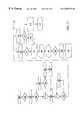
- the present shared memory systemis shown in FIG. 1 as comprising shared memory unit (SMU) 100 , and multiple computer systems 200 , each connected by links 101 , to the SMU.
- SMUshared memory unit
- the SMUis a freestanding unit containing shared memory accessible by all connected computer systems 200 via its I/O ports and a cable or bus.
- Each computer system 200may comprise a conventional personal computer or workstation, such as an IBM-PC compatible computer.
- Each computer system 200includes conventional local memory 201 , which may comprise one or more memory modules closely coupled to the processor on the system motherboard and alternatively, or in addition, one or more memory expansion boards coupled to the system bus.
- each computer system connected to the SMUincludes a memory alias adapter (MAA) 300 (shown extended for illustrative purposes only) coupled to the computer system's processor.
- MAAmemory alias adapter
- Each MAAprovides full physical, electrical and operational emulation of a traditional memory device, such as a memory board coupled, for example, to a standard computer bus, such as the PCI (Peripheral Component Interconnect) bus.
- the MAAmay comprise a SIMM/DIMM memory module, closely coupled to the computer's processor via a socket proximate the processor.
- Each MAAincludes an I/O port to connect the MAA to the SMU 100 via a cable or bus.
- the MAAis assigned a (preferably contiguous) range of memory addresses. Whenever a computer system performs a memory-write operation to a region of memory corresponding to the physical address space locally assigned to the MAA 300 (as opposed to local memory 201 ), the MAA responds by placing the write data, together with the associated address, upon the network link to the SMU. The SMU responds by storing the specified write data at the appropriate address within its own memory. In this manner, memory write operations that appear to be local operations to the computer's processor are, in fact, memory write operations to a central shared memory unit.
- the MAAWhenever a computer system performs a memory-read operation to a region of memory corresponding to the physical address space locally assigned to the MAA, the MAA responds by sensing a request for data, together with the associated address to the SMU. The SMU responds to this request by retrieving the requested data from its shared memory, at the requested address. The requested data is then sent back to the requesting computer system. The computer system's MAA receives the requested data, and places it upon the computer's system bus. In this manner, memory read operations that appear to be local operations to the computer's processor are, in fact, memory read operations from a central shared memory unit.
- the MAAresponds by sending a data write request, including the associated address and data to the SMU.
- the SMUresponds to this request by storing the messaged data into its shared memory, at the specified address.
- An acknowledgementis then sent back to the requesting computer system. link.
- the computer system's MAAreceives the acknowledgement, and places an appropriate handshake signal upon the computer's system bus in order to complete the memory access cycle.
- memory write operations that appear to be local operations to the computer's processorare, in fact, memory write operations to a central shared memory unit.
- a preferred embodiment of MAA 300is shown in FIG. 2 as comprising address detect ASIC (Application Specific Integrated Circuit) 310 and interface control ASIC 350 .
- a conventional PCI edge connector 301is provided for exchanging address, data and control signals with the system processor when MAA 300 is inserted into an empty PCI slot within the computer system.
- Address detect ASIC 310provides overall PCI bus interface functions for the MAA, coupling to the PCI edge connector via on-board bus 302 . This ASIC senses PCI bus activity, determining when processor write (store) operations or read (load) operations correspond to memory addresses assigned to the MAA and, in turn, to the SMU. When such processor operations are detected, a transaction manager within ASIC 310 passes the address and data corresponding to the operation to interface control ASIC 350 via a dedicated interface 303 .
- Interface control ASIC 350provides link management functions between the MAA and the SMU in the form of memory read/write requests sent to the SMU through I/O port 304 and over the cable or bus 101 .
- interface control ASIC 350receives the operation's associated address and data information from address detect ASIC 310 via interface 303 .
- Interface control ASIC 350translates the address and data into a shared memory write request, and handles transmitting the message over the physical layer of the connection to the SMU.
- the interface control ASICreceives response messages, such as indications of successful writes into shared memory, from the SMU. Such acknowledgements are passed back to address detect ASIC 310 via interface 303 .
- Address detect ASIC 310uses this acknowledgement to complete the overall write operation occurring on the PCI bus.
- interface control ASIC 350receives the operation's associated address information from address detect ASIC 310 via interface 303 .
- Interface control ASIC 350translates the address into a shared memory read request, and handles transmitting the request over the physical layer of the connection to the SMU.
- the interface control ASICreceives response requests, such as those containing data stored within the requested address of the SMU's shared memory, from the SMU.
- the datais passed back to address detect ASIC 310 via interface 303 .
- Address detect ASIC 310places this data upon the PCI bus via edge connector 301 to complete the overall read operation occurring on the PCI bus.
- PCI interface 320which may be a PCI target/slave unit, or a unit capable of mastering the PCI bus, may comprise an “off the shelf” intellectual property core, obtainable commercially from a number of vendors, including Xilinx, Inc. Alternatively, PCI interface 320 may be separated from ASIC 310 as a stand-alone component. Such devices are commercially available, from vendors such as Applied Microcircuits Corporation.
- a typical PCI interface 320includes a PCI protocol handler 321 , PCI configuration manager 322 , PCI configuration storage 323 , buffer memory 324 , and PCI to local I/O bus interface 325 .
- Protocol handler 321provides the overall interface to the PCI physical layer, via onboard bus 302 .
- the PCI configuration manager 322provides the required PCI-compliant configuration registers (Vendor ID, Device ID, memory requirements, etc.), polled by the host's BIOS system during power-on initialization. The device-specific data is stored within PCI configuration storage 323 .
- PCI to local I/O bus transfer interface 325provides a bridge between the complex PCI bus and the simplified, internal local I/O bus 326 .
- a buffer memory 324provides mailbox registers and pass-through buffering between the PCI bus 302 and local bus 326 .
- the MAAhas focused on the use of a Peripheral Component Interface (PCI) bus to electrically and physically couple the MAA to a standard PCI expansion bus of a personal computer or computer workstation, such as an IBM-PC compatible computer.
- PCIPeripheral Component Interface
- other standard expansion bussesmay be used.
- the MAAmay be coupled to the Advanced Graphics Port (AGP) of a computer, rather than the PCI bus.
- AGPAdvanced Graphics Port
- the AGP standard expansion busmay be preferred over the PCI, inasmuch as the AGP generally provides a faster, higher bandwidth connection to the processor itself.
- the address detect ASICshould include a conventional AGP interface, rather than a conventional PCI interface.
- PCI interface 320 within address detect ASIC 310is replaced with a conventional AGP interface.
- AGP interfacesare commercially available in the form of a synthesizable core for incorporation as a component within an overall ASIC.
- Commercially available AGP coresinclude the SuperAGPTargetCore from Integrated Intellectual Property, Inc. of Santa Clara, Calif., as well as the AGP Master Core product from Phoenix Technologies, Ltd. Of San Jose, Calif.
- ISAIndustry Standard Architecture
- SIMM/DIMM memory expansion socketsmay also be used.
- a suitable matching bus interfacemust be included within the address detect ASIC of the MAA, as well as a suitable matching edge connector on the MAA circuit card.
- Transaction unit 330is shown in FIG. 3 as including local I/O bus interface 331 , buffer memory 332 and transaction manager 333 .
- Local I/O bus interfaceprovides the physical interface to local I/O bus 331 accepting, among other things, processor write and processor read operations.
- Transaction manager 333monitors the accepted local I/O bus operations, looking for operations associated with the shared memory region of the local processor's overall memory map.
- Transaction manager 333contains an address limit register, containing a value representing a boundary address between the top of memory local to the present processor, and higher memory addresses, corresponding to shared memory contained within the SMU.
- the transaction manageralso contains an address request register, for storing the address corresponding to the current memory access operation on the PCI bus, and a magnitude comparator coupled to these two registers for comparing their relative values.
- Buffer memory 332provides storage for ongoing transactions within the transaction manager.
- Interface 303includes paths for both SMU memory requests 334 and SMU memory responses 335 .
- SMU read operationsthe requests include the SMU memory address, and the responses include the contents of the relevant SMU memory location.
- SMU write operationsthe requests include both the SMU memory address and the data to be written, and the responses include acknowledgements that the data has been successfully written.
- Interface control ASIC 350is shown in further detail in FIG. 4 as comprising link manager 351 and I/O port physical interface 352 .
- Link manager 351provides overall processing of SMU memory access from the Memory Alias Adapter.
- This ASIC 350is coupled to the address detect ASIC via interface 303 , including paths for both SMU memory requests 334 and SMU memory responses 335 .
- the link managermaps SMU memory requests into messages suitable for transmission over bi-directional data port 304 and, in turn, the network link between the MAA and the SMU. This preferably includes the generation of error detection and correction information within the messages, such as conventional Cyclical Redundancy Check (CRC) information.
- CRCCyclical Redundancy Check
- the link manageris controlled by traditional, dedicated state machine circuitry within the ASIC.
- a conventional microprocessor coremay be included within the ASIC, with microprocessor firmware stored within the ASIC controlling the link operations between the ASIC and the SMU.
- microprocessor coresare commercially available, such as the MCORE family from Motorola, Inc.
- physical interface 352provides the bridge between the link manager 351 and data port 304 and, in turn, the connection link between the MAA and the SMU.
- the choice, and design of physical interface 352depends upon the choice of physical interconnect to the SMU. In a preferred embodiment, for very close proximaty to a crossbar switch, a parallel, high speed connection link is recommended, such as the ANSI/IEEE standard Scalable Coherent Interface (SCI). In such cases, physical interface 352 comprises a conventional SCI interface.
- SCIScalable Coherent Interface
- SCSISmall Computer System Interfaces
- SCSI2Small Computer System Interfaces
- UltraSCSIa commercially available host adapter may be used for physical interface 352 , such as the AIC-7895 product from Adaptec, Inc. of Milpitas, Calif.
- suitable serial linkmay alternatively be used.
- suitable serial linksinclude the Institute of Electrical and Electronic Engineers (IEEE) standard 1394 (also shown as FireWire) and Ethernet.
- IEEE-1394is chosen, physical interface 352 preferably comprises a conventional IEEE-1394 host adapter device, such as the AIC-5800 device from Adaptec, Inc. of Milpitas, Calif.
- physical interface 352preferably comprises a conventional Ethernet media access controller (MAC) and Ethernet physical interface (PHY).
- MACEthernet media access controller
- PHYEthernet physical interface
- link manager 351issues SMU access requests 353 and link-level requests 354 to the physical interface.
- the physical interfacewill respond with access grant signals 355 , which, in turn, causes the link manager to issue an acknowledgement 357 .
- the physical interfacewill issue link-level responses 358 and network system configuration information 359 to the link manager, which issues acknowledgements 356 .
- FIG. 5shows the system bring-up sequence 360 for the MAA.
- state 361the local memory in the individual processors in the overall system is detected.
- state 362the amount of local memory in each processor is mapped.
- state 363the minimum and maximum local memory addresses for the processor is established.
- state 364the local/shared memory transition address is selected.
- this local/shared memory transition addressis stored into the address limit register of the transaction manager portion of the MAA's address detect ASIC.
- a shared memory access operationbegins in state 371 , where the processor issues a data request, in the form of a memory read (load) or memory write (store) operation.
- the processorissues the memory address for the data request upon its address bus.
- PCI bridge circuitrytypically proximate processor on its motherboard, translates the data request into PCI bus signals, which are made available to the MAA in its PCI bus slot.
- the MAAloads the address from the PCI bus into its address request register within the address detect ASIC.
- state 375the contents of the address request register are compared to the contents of the address limit register. Action is taken, based upon the output of this comparison, within state 376 . If the contents of the address request register are less than the contents of the address limit register, transition is taken to state 377 . Within state 377 , the current PCI bus transaction is deemed to be a local access, requiring no further MAA intervention. Transaction is taken to state 368 , where MAA processing of the current PCI bus operation is halted. The MAA will then await the next PCI bus operation, which will begin again at state 371 . If, however, the contents of the address request register is greater than or equal to the contents of the address limit register, transition is taken from state 376 to state 379 .
- the current PCI bus operationis deemed to be a shared memory access.
- the contents of the address detect registeris passed from the address detect ASIC to the interface control ASIC, together with an indication of whether the current operation is a memory read or a memory write. If the current operation is a memory write, the data to be written is also passed to the interface control ASIC at this time.
- the operation of the interface control ASICgoverned by the state machine controller within its transaction manager, is shown in FIG. 7 .
- the controllerstays within state 385 , awaiting data from the address detect ASIC.
- an address(and associated data, for write operations) is received from the address detect ASIC, transition is taken to state 386 .
- an address tagis generated. Any suitable hashing algorithm may be used to generate the tag, which is used as an index for storing information relating to the pending operation within the interface control ASIC's buffer memory.
- a connection to the SMUvia the ASIC's physical interface and the dedicated network link
- the systemwill remain within state 387 until a grant message is received, at which time a transition is taken to state 388 .
- the SMU memory addresstogether with the corresponding data (for memory write operations), is sent to the SMU. If the current operation is a memory write operation, an acknowledgement is sent from the interface control ASIC to the address detect ASIC at this time, indicating a successful shared memory write operation.
- the MAAis capable of handling multiple outstanding (i.e., simultaneous and overlapping) connection requests to the SMU.
- transitionis taken from state 388 to state 389 , where the MAA waits for a response from the SMU.
- the MAAtests to see if an SMU response has been received by the physical interface portion of the interface control ASIC. If no response is received, transition is taken back to state 389 . If, however, a response is received, transition is taken to state 391 , where the tag portion of a received request from the SMU is matched against the tags associated with pending requests, stored within the ASIC's memory buffer.
- state 392the data from the request received from the SMU is placed on the internal data bus connecting the interface control ASIC and the address detect ASIC.
- a link level response messageis issued to the address detect ASIC, indicating that the requested data from the SMU is available.
- the interface controller ASIC's state machinehas completed the shared memory read operation, and transition is taken back to the idle state 385 to await the next request from the address detect ASIC.
- the link level response requestincluding the data requested from the specified SMU memory address, is received by the address detect ASIC at state 380 .
- this ASICasserting the PCI TRDY signal and then transition is taken to state 382 , where the requested data from the SMU is placed upon the PCI data bus.
- state 383the processor loads the requested data into one of its internal operations, completing the shared memory read operation.
- the MAAis coupled to a computer running a conventional uniprocessor operating system, such as a uniprocessor build of the Windows NT operating system, distributed by Microsoft Corp. of Redmond, Wash.
- a set of operating system (OS) enhancementsin the form of an operating system extension layer, is employed to facilitate use of the MAA and the SMU by programmers of applications running on the operating system.
- the OS extension layerexposes an application programming interface (API) for use by the application programmer.
- APIapplication programming interface
- the APIpermits the programmer to specify the range of local memory addresses which actually correspond to external physical memory located within the SMU.
- the APIexposes functions which permit the user to define, allocate, and manage the SMU's memory.
- the OS extension layermakes low-level calls to another API, provided by the operating system kernel, including kernel-mode and hardware abstraction layer (HAL) API calls.
- the OS extension layerforms a bridge between the user applications and the operating system, facilitating the application programmer's usage of shared memory, supplied to the computer by the SMU via the computer's local MAA.
- BIOSBasic Input/Output Operating System
- a fundamental function of most system BIOS programsis to test local memory, and inform any subsequently bootstrapped operating system of the amount of available memory, Since a conventional BIOS is not cognizant of the additional memory within the SMU and made available to the processor via its local MAA, the conventional BIOS only indicates the amount of local memory.
- BIOSmay be readily modified to indicate to any subsequently-booted operating system that there is an amount of available memory which comprises an aggregate of the physical memory coupled to the motherboard and the total physical memory of the SMU, available via the standard expansion bus to which the MAA is coupled.
- a particular computer systemhas 128 Megabytes (MB) of local memory, and includes an MAA coupled to its PC 1 bus.
- the MAAin turn, is linked to an SMU having an additional 128 MB of memory.
- the modified system BIOSwould be hard coded to inform any subsequently-booted operating system that there is a total of 256 MB of (apparently) local memory—128 MB coupled to the local memory bus, and 128 MB coupled to the local PCI bus.
- a second processorhaving only 64 MB may also be coupled to the SMU.
- the first 64 MBcomprises its local memory.
- the next 64 MBcomprises an unused and unavailable “hole” within its overall memory space.
- the next 128 MBcomprises the shared memory of the SMU.
- Applications running on this second processormay be informed of this discontinuous memory space by executing a memory map inquiry API call to an OS extension layer.
- a modified BIOSmay inform the application of the ranges of available memory. In either case, discontinuous memory spaces are supported by the present invention.
- the SMUis shown in further detail in FIG. 8 as comprising shared memory banks 110 , crossbar switch 150 , and memory controller/processor interconnect 400 .
- Memory controller/processor interconnect 400includes several physical interface components, each similar to the physical interface portion of the MAA's interface control ASIC. Each physical interface component provides the SMU with a port, connecting the SMU to one of the computer systems via a dedicated cable or bus 101 . As with the interface control ASIC, the design of the memory controller/processor interconnect's physical interface will depend upon the type of cable or bus 101 selected (i.e., SCI, ATM, FibreChannel, Ethernet, etc.). Moreover, although three such ports are shown in FIG. 8 for illustrative purposes, it is contemplated that a large number of such connections (64 or greater) may be provided.
- memory controller/processor interconnect 400also includes a state machine for controlling both memory read operations and memory write operations to the memory banks 110 , in response to access requests [messages] received over the cable or bus 101 .
- Crossbar switch 150is of the non-blocking variety, and is interposed between memory controller/processor interconnect 400 and memory banks 110 in order to provide multiple, simultaneous accesses to the shared memory.
- Memory banks 110are shown in further detail in FIG. 9 as including a plurality of identically sized, individual memory banks 111 , each coupled to a common address bus 112 .
- the lower order bits of address bus 112are used to address the memory contents of each bank 111 .
- the highest order bits of address bus 112are decoded to selectively enable one of the multiple memory banks.
- four memory banksare shown in FIG. 9 for illustrative purposes, it is contemplated that a large number of such banks (64 or greater) may be provided.
- Non-blocking crossbar switch 150is shown in further detail in FIG. 10 as including switch controller 151 , read port address bus 152 , write port address bus 153 , read port multiplexers 154 , write port multiplexers 155 , memory controller ports 156 , and memory bank ports 157 .
- Each memory controller port 156provides an individual data path between crossbar switch 150 and the memory controller/processor interconnect, via a corresponding data path 158 .
- crossbar switch 150preferably includes one memory controller port for each connection coupled to the memory controller/processor interconnect portion of the SMU.
- Each memory bank port 157provides an individual data path between crossbar switch 150 and one of the memory banks, via a corresponding data path 159 .
- crossbar switch 150preferably includes one memory bank port for each individual memory bank within the SMU.
- switch controller 151In response to shared memory read requests forwarded from the memory controller/processor interconnect portion of the SMU, switch controller 151 places high order address information upon read port address bus 152 and, in turn, to the select inputs of the read port multiplexers 154 . At this time, switch controller 151 commands one of the read port multiplexers 154 , corresponding to the desired target memory controller port, to latch its current select inputs and, in turn, to latch the contents of the read port address bus. Since each read port multiplexer accepts data inputs from each of the memory bank ports, this causes the selected multiplexer to provide a data link, through the crossbar switch, from one memory bank port to one memory controller port.
- switch controller 151may now change the contents of read port address bus 152 , in order to provide another, non-blocking read link between one of the memory bank ports and a different memory controller port 156 . This is accomplished by commanding a different read port multiplexer 154 corresponding to another target memory controller port, to again latch its current select inputs.
- crossbar switch 150provides multiple, simultaneous data paths from the memory banks to the memory controller/processor interconnect portion of the SMU. This, in turn, permits multiple, overlapping read access to the shared memory.
- switch controller 151In response to shared memory write requests forwarded from the memory controller/processor interconnect portion of the SMU, switch controller 151 places high order address information upon of write port address bus 153 and, in turn, to the select inputs the write port multiplexers 155 . At this time, switch controller 151 commands one of the write port multiplexers 155 , corresponding to the desired target memory bank port, to latch its current select inputs and, in turn, to latch the contents of the write port address bus. Since each write port multiplexer accepts data input from each of the memory controller ports, this causes the selected multiplexer to provide a data link, through the crossbar switch, from one memory controller port to one memory bank port.
- switch controller 151may now change the contents of write port address bus 153 , in order to provide another, non-blocking write link between one of the memory controller ports and a different memory bank port 157 . This is accomplished by commanding a different write port multiplexer 155 corresponding to another target memory bank port, to again latch its current select inputs.
- crossbar switch 150provides multiple, simultaneous data paths from the memory controller/processor interconnect portion of the SMU to the memory banks. This, in turn, permits multiple, overlapping write operations to the shared memory.
- the SMUprovides the means for performing atomic (i.e., locked/uninterruptable) memory operations between processor nodes and the shared memory, by permitting a processor node to temporarily lock a region of shared memory and block other node accesses.
- FIG. 10shows three read port multiplexers 154 and three write port multiplexers for illustration purposes, many more, on the order of 64 or more, are contemplated. Note that one read port multiplexer is required for each individual bank within the SMU's memory banks; and that one write port multiplexer is required for each physical interface (and dedicated network link) within the SMU's memory controller/processor interconnect circuitry.
- memory controller/processor interconnectalso includes a state machine for controlling both memory read operations and memory write operations to the memory banks 110 , in response to access requests received over the cable or bus 101 .
- the state diagram of the state machine controller portion of memory controller/processor interconnect 400is shown in FIG. 11 .
- a conventional microprocessor coremay be included as a separate entity or within the controller's ASIC, with microprocessor firmware controlling the physical interface components, crossbar switch and memory banks.
- the memory controller's idle stateis state 401 , where the controller continuously tests each of the several physical interface components for a new memory request. The result of each test is handled in state 402 . If no new request is detected, transition is taken back to state 401 . If, however, a new memory request is detected, transition is taken to state 403 , where another test is conducted to determine if one or more overlapping requests are in progress. The results of this test are acted upon in state 404 . If overlapping requests are detected, transition is taken to state 405 , where the overlapping requests and the new request are compared, to determine if the new request is for access to the same memory bank as one of the already-pending requests.
- Each request's associated memory bankis determined by decoding the higher-order address bits of the shared memory address specified within the overall request message.
- State 406takes action upon the results of this test. If a memory bank overlap occurs, transition is taken to state 407 , where the current memory request is arbitrated against the overlapping request for the same memory bank. In state 408 , an active request is selected from among all pending requests for the same bank, and transition is taken to state 409 to determine if the requested memory bank is still locked.
- State 409can also be reached from state 404 , if no overlapping requests are detected. However when state 409 is reached, action is taken on its test in state 410 . If the memory bank is still locked, transition is taken to state 411 , where the lock is retested. If, however, there is no active lock on the selected memory bank, transition is taken to state 412 , where a test is performed to determine whether the current shared memory request is a write operation or a read operation. The results of this test are acted upon within state 413 . If the operation is a write operation, transition is taken to state 414 , where the use table is updated, and state 415 , where the data write request is forwarded to the controller portion of the crossbar switch.
- transitionis taken to state 416 , where the use table is consulted to determine if the current read address is “stale”. The result of this test is acted upon in state 417 . If the determination is “stale”, transition is taken to state 418 to update the data. Otherwise, transition is taken to state 419 , where the use table is updated.
- transitionis taken to state 420 , where the read request is forwarded to the controller portion of the crossbar switch.
- state 421continuously senses the crossbar switch controller for an indication that data from a pending operation is available. The results of each such test is acted upon in state 422 . If no data is available, transition is taken back to state 421 for continual sensing. If, however, read data is available, transition is taken to state 423 , where the read data is matched with its associated tag information. In state 424 , the read and tag data are formatted into a message for transmission back to the requesting MAA via the dedicated network link.
- the interconnected processorsare more closely integrated, residing within a common enclosure.
- the shared memoryis distributed into regions associated with each system processor, rather than centralized, as is the prior embodiment.
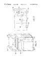
- This embodimentis shown in FIG. 12 as comprising system enclosure 500 , motherboard 501 , power supplies 504 , and hard file bays 505 .
- Power supplies 504preferably include two or more redundant supplies.
- file bays 505preferably include a configuration of redundant hard disk drives, such as mirrored drives or RAID (Redundant Array of Inexpensive Drives).
- Motherboard 501includes multiple data busses, including conventional system bus 502 and shared memory interconnect bus 503 .
- Conventional system bus 502which may comprise a conventional PCI bus, is used by each system processor to access common devices and peripherals.
- Such devices and peripheralsmay include, among other things, display controllers, modems, and disk drive controllers which, in turn, access disk drives within file bays 505 .
- Shared memory interconnect bus 503is preferably a high speed, low latency interconnect, such as the standard SCI bus.
- motherboard 501includes sockets for accepting a plurality of processor cards 600 .
- Each socketcouples a processor card 600 to both the system bus 502 and the shared memory interconnect bus 503 .
- processor cardsare shown in FIG. 12 for illustrative purposes, motherboards capable of accepting a large number of processor cards, such as 64 or more, are contemplated.
- each processor card 600includes a region of shared memory, which it makes available to all of the other processors in the system.
- Each processordynamically configures its portion of the overall shared memory to reside at a different global memory address, relative to all of the other processor's own portions of shared memory.
- each processor cardcan individually address and access the shared memory portions of all the other processor cards.
- a processor card 600is shown in FIG. 13 as comprising processor and support circuitry 601 , local memory 602 , shared memory 603 , and Memory Bus Transfer controller (MBT) 610 .
- Processor 601may be a typical microprocessor, such as an Intel Pentium, together with its support circuitry, or “chip set”.
- the processor's support circuitryincludes support for a local memory bus 604 , and a bus controller for communicating on the PCI bus 502 .
- Local memory bus 604allows the processor to access two separate regions of on-board memory. Local memory 602 may only be accessed by processor 601 .
- Shared memory 603may be accessed both by the local processor 601 , and other processors residing on other cards within the system, via shared memory interconnect bus 503 .
- MBT 610is situated between shared memory 603 , local memory bus 604 , and shared memory interconnect bus 503 .
- a dedicated data, address and control bus 605couples MBT 610 to the shared memory portion 603 of the processor's memory.
- MBT 610controls accesses to the local shared memory from both local processor 601 and other processors which request access to shared memory 603 via shared memory interconnect bus 503 .
- MBT 610also permits its local processor 601 to access the shared memory portions of other processor cards.
- the MBTmonitors the address specified by its local processor whenever a memory request (read or write) is placed on the local memory bus. If the request is for local non-shared memory, private to the processor, no MBT intervention is necessary.
- the processoraccesses its local memory via its local memory bus.
- the MBTperforms the requisite memory access. For memory writes, an acknowledgement, or handshake, is returned to the local processor, via the local memory bus. For memory reads, the handshake is accompanied by the requested data. If, however, the local processor is addressing memory shared by another processor card, the MBT places a corresponding request (read or write) on the shared memory interconnect bus. For memory write operations, the associated data accompanies the request. When the MBT accepts a response over the shared memory interconnect bus, it relays the results to the local processor. For memory read operations, this response includes the requested data. For memory write operations, the response is an acknowledgement, or handshake.
- each MBTalso monitors the shared memory interconnect bus for requests from other processors (via their own MBTs) for access to the portion of shared memory coupled to the MBT.
- Each MBTservices appropriate requests, performing shared memory writes and reads, and transmitting associated data and handshake/acknowledgements, over the shared memory interconnect bus.
- the MBTcomprises an ASIC, and includes traditional, dedicated state machine circuitry controlling overall operation of the MBT.
- a conventional microprocessor coremay be included within the MBT ASIC, with microprocessor firmware controlling memory access to the on-board shared memory, as well as the on-board processor's requests to off-board shared memory.
- the MBT ASICincludes a physical interface circuit. This circuit forms the bridge between the MBT and the shared memory interconnect bus.
- the physical interfaceincludes an interface to the SCI bus within the MBT ASIC.
- the SCI interfacemay comprise an external SCI interface device, such as those commercially available from LSI Logic Corp. of Milpitas, Calif.
- FIG. 14shows the system bring-up sequence 620 for the processor card.
- state 621upon system power-up, the amount of local memory in each processor is mapped.
- state 622registers within the MBT are loaded with these local and shared address ranges.
- state 623the upper address boundary of local memory is written to a register within the MBT, named LREG; the shared memory low address boundary is written to an MBT register named SREGL, and the shared memory high address boundary is written to an MBT register designated SREGH.
- a memory access transactionbegins with a processor issuing a (load or store) data request.
- the processorgenerates the effective address for the relevant memory location and, in state 633 , places the address together with its associated control and (for write operations) data on the processor card's local memory bus.
- the MBTloads the address from the local memory bus into its address request register, designated ARR.
- state 635the MBT compares the contents of the ARR and LREG registers, and the result of the comparison is acted upon in state 636 . If ARR is less than or equal to LREG, transition is taken to state 637 , where the memory access is deemed to be to local memory. In state 638 , the MBT processing of the current processor request is halted, since no further MBT action is warranted. The MBT will then await the next processor memory request, beginning again at state 631 .
- transitionis taken from state 636 to state 639 .
- the MBTcompares the contents of the ARR and SREGH registers. If ARR is greater than SREGH, the memory access is deemed to be to a portion of shared memory which resides on a different processor card. Transition is taken to state 640 , where a tag associated with the memory request is generated.
- the MBTrequests access to the shared memory interconnect bus, in order to issue the memory request.
- state 642the MBT tests whether access to the bus was granted. If not, transition is taken back to state 640 , in order to retry the bus request.
- transitionis taken to state 643 , where the MBT issues the request onto the bus.
- Transitionis taken to state 644 , where the MBT waits for a response (data plus handshake/acknowledge for memory reads, handshake/acknowledge only for memory writes) over the bus.
- the MBTdetermines that ARR is less than or equal to SREGH, the memory access is deemed to be to shared memory located on the processor card. Transition is then taken to state 651 , discussed in reference to FIG. 16 .
- FIG. 16shows the MBT processing of accesses to the portion of overall shared memory situated on its own processor card. Processing of memory requests from both the on-board processor (via the local memory bus) and from external processors (via the shared memory interconnect bus) are shown.
- state 651the MBT tests both the local memory bus and the shared memory interconnect bus for a memory access request for its assigned (i.e., on board) portion of overall shared memory. The result of the test is acted upon in state 652 , where transition is taken either back to state 651 , if such shared memory access is requested, or to state 653 , if a shared memory request is detected.
- state 653a test is performed to determine if the requesting processor is the local (on-board) processor. The result of the test is acted upon in state 654 , where transition is taken to state 655 if the requesting processor is local, or to state 656 if the requesting processor is off-board. In state 655 , a tag is generated for the local processor's memory request, and transition is taken to state 656 .
- a testis made to determine if multiple requests are pending for the MBT's portion of shared memory. The result of the test is acted upon in state 657 . If multiple requests are pending, transition is taken to state 658 , where the requests are arbitrated. Following arbitration, or if no overlapping requests were detected, transition is taken to state 659 , where the MBT tests whether there is a lock (via a semaphore) on the requested memory location. The result of this test is acted upon in state 660 . If there is an active lock, transition is taken to state 661 , in order to wait for the lock to be released, and then back to state 659 , where the lock is retested.
- transitionis taken to state 671 , where the MBT tests whether the current request is a memory read or write operation. The result of this test is acted upon in state 672 . If the request is a write request, transition is taken to state 673 , where the MBT writes the data accompanying the memory request to the specified address within its portion of shared memory. Transition is taken to state 674 , where the use table is updated to reflect the memory access, and then to state 675 , where the memory write operation is deemed completed.
- transitionis taken to state 676 , where the use table is consulted to determine if the current read address is “stale”. The result of this test is acted upon in state 677 . If the determination is “stale”, transition is taken to state 678 to update the data. Otherwise, or after updating the data, transition is taken to state 679 , where the data within the specified address in shared memory is read.
- state 680the use table is updated. Transition is taken to state 681 , where the tags from the use table and data requests are matched.
- the MBTtests whether the processor issuing the current request is the local (on-board) processor. The result of this test is acted upon in state 683 .
- transitionis taken to state 684 , where the requested data, together with appropriate acknowledge/handshaking signals, are placed on the local processor's memory bus. If, however, the requesting processor is off-board, transition is taken to state 685 , where the MBT requests the shared memory interconnect bus, then waits until the bus is granted. Upon receiving a bus grant indication, transition is taken to state 686 , where the MBT places the requested data, together with appropriate acknowledge/handshaking signals, onto the shared memory interconnect bus, where it is subsequently retrieved by another MBT associated with the requesting processor.
Landscapes
- Engineering & Computer Science (AREA)
- Theoretical Computer Science (AREA)
- Physics & Mathematics (AREA)
- General Engineering & Computer Science (AREA)
- General Physics & Mathematics (AREA)
- Multi Processors (AREA)
Abstract
Description
Claims (16)
Priority Applications (8)
| Application Number | Priority Date | Filing Date | Title |
|---|---|---|---|
| US09/273,430US6295571B1 (en) | 1999-03-19 | 1999-03-19 | Shared memory apparatus and method for multiprocessor systems |
| PCT/US2000/001262WO2000057286A1 (en) | 1999-03-19 | 2000-01-18 | Shared memory apparatus and method for multiprocessor systems |
| CA002367065ACA2367065A1 (en) | 1999-03-19 | 2000-01-18 | Shared memory apparatus and method for multiprocessor systems |
| AU26183/00AAU2618300A (en) | 1999-03-19 | 2000-01-18 | Shared memory apparatus and method for multiprocessor systems |
| IL14553100AIL145531A0 (en) | 1999-03-19 | 2000-01-18 | Shared memory apparatus and method for multiprocessor systems |
| EP00904420AEP1166209A1 (en) | 1999-03-19 | 2000-01-18 | Shared memory apparatus and method for multiprocessor systems |
| US09/854,351US6519672B2 (en) | 1999-03-19 | 2001-05-10 | Shared memory apparatus and method for multiprocessor systems |
| US09/859,193US6467011B2 (en) | 1999-03-19 | 2001-05-15 | Shared memory apparatus and method for multiprocessor systems |
Applications Claiming Priority (1)
| Application Number | Priority Date | Filing Date | Title |
|---|---|---|---|
| US09/273,430US6295571B1 (en) | 1999-03-19 | 1999-03-19 | Shared memory apparatus and method for multiprocessor systems |
Related Child Applications (2)
| Application Number | Title | Priority Date | Filing Date |
|---|---|---|---|
| US09/854,351DivisionUS6519672B2 (en) | 1999-03-19 | 2001-05-10 | Shared memory apparatus and method for multiprocessor systems |
| US09/859,193ContinuationUS6467011B2 (en) | 1999-03-19 | 2001-05-15 | Shared memory apparatus and method for multiprocessor systems |
Publications (1)
| Publication Number | Publication Date |
|---|---|
| US6295571B1true US6295571B1 (en) | 2001-09-25 |
Family
ID=23043905
Family Applications (3)
| Application Number | Title | Priority Date | Filing Date |
|---|---|---|---|
| US09/273,430Expired - LifetimeUS6295571B1 (en) | 1999-03-19 | 1999-03-19 | Shared memory apparatus and method for multiprocessor systems |
| US09/854,351Expired - LifetimeUS6519672B2 (en) | 1999-03-19 | 2001-05-10 | Shared memory apparatus and method for multiprocessor systems |
| US09/859,193Expired - LifetimeUS6467011B2 (en) | 1999-03-19 | 2001-05-15 | Shared memory apparatus and method for multiprocessor systems |
Family Applications After (2)
| Application Number | Title | Priority Date | Filing Date |
|---|---|---|---|
| US09/854,351Expired - LifetimeUS6519672B2 (en) | 1999-03-19 | 2001-05-10 | Shared memory apparatus and method for multiprocessor systems |
| US09/859,193Expired - LifetimeUS6467011B2 (en) | 1999-03-19 | 2001-05-15 | Shared memory apparatus and method for multiprocessor systems |
Country Status (6)
| Country | Link |
|---|---|
| US (3) | US6295571B1 (en) |
| EP (1) | EP1166209A1 (en) |
| AU (1) | AU2618300A (en) |
| CA (1) | CA2367065A1 (en) |
| IL (1) | IL145531A0 (en) |
| WO (1) | WO2000057286A1 (en) |
Cited By (64)
| Publication number | Priority date | Publication date | Assignee | Title |
|---|---|---|---|---|
| US20020013822A1 (en)* | 2000-07-26 | 2002-01-31 | West Karlon K. | Shared as needed programming model |
| US20020019926A1 (en)* | 1997-12-17 | 2002-02-14 | Huppenthal Jon M. | Switch/network adapter port for clustered computers employing a chain of multi-adaptive processors in a dual in-line memory module format |
| US6405293B1 (en)* | 2000-03-21 | 2002-06-11 | Oak Technology, Inc. | Selectively accessible memory banks for operating in alternately reading or writing modes of operation |
| WO2002088970A1 (en)* | 2001-05-02 | 2002-11-07 | Portalplayer, Inc. | Crossbar multipath resource controller system and method |
| US20030140192A1 (en)* | 2000-03-31 | 2003-07-24 | Thibault Robert A. | Data storage system |
| US20030233398A1 (en)* | 2002-06-12 | 2003-12-18 | Kinstler Gary A. | Distributed data handling and processing resources system |
| US20040015656A1 (en)* | 2002-07-19 | 2004-01-22 | Rust Robert A. | Hardware assisted communication between processors |
| US20040019703A1 (en)* | 1997-12-17 | 2004-01-29 | Src Computers, Inc. | Switch/network adapter port incorporating shared memory resources selectively accessible by a direct execution logic element and one or more dense logic devices |
| US6687797B1 (en)* | 2001-05-17 | 2004-02-03 | Emc Corporation | Arbitration system and method |
| US6763327B1 (en)* | 2000-02-17 | 2004-07-13 | Tensilica, Inc. | Abstraction of configurable processor functionality for operating systems portability |
| US6772328B1 (en)* | 1999-06-18 | 2004-08-03 | Samsung Electronics Co., Ltd. | Dynamic initialization of processor module via motherboard interface |
| US20040181471A1 (en)* | 2003-03-12 | 2004-09-16 | Microsoft Corporation | Automated business software application integration |
| US6823475B1 (en)* | 1999-11-15 | 2004-11-23 | Robin Harker | PC-CPU motherboards with common fault-tolerant power supply |
| US20040236877A1 (en)* | 1997-12-17 | 2004-11-25 | Lee A. Burton | Switch/network adapter port incorporating shared memory resources selectively accessible by a direct execution logic element and one or more dense logic devices in a fully buffered dual in-line memory module format (FB-DIMM) |
| US20050080961A1 (en)* | 2003-10-09 | 2005-04-14 | Bedwell Ryan D. | Communication steering for use in a multi-master shared resource system |
| US6885631B1 (en)* | 1999-07-01 | 2005-04-26 | Samsung Electronics Co., Ltd. | Connection management method for digital interface |
| US6907483B1 (en) | 2002-03-28 | 2005-06-14 | Emc Corporation | Data storage system having dummy printed circuit boards with jumpers |
| US20050283546A1 (en)* | 1997-12-17 | 2005-12-22 | Huppenthal Jon M | Switch/network adapter port coupling a reconfigurable processing element to one or more microprocessors for use with interleaved memory controllers |
| US7036106B1 (en) | 2000-02-17 | 2006-04-25 | Tensilica, Inc. | Automated processor generation system for designing a configurable processor and method for the same |
| US20060095718A1 (en)* | 2004-09-16 | 2006-05-04 | International Business Machines Corporation | System and method for providing a persistent function server |
| US20060215434A1 (en)* | 2003-05-08 | 2006-09-28 | Lee Terry R | Apparatus and methods for a physical layout of simultaneously sub-accessible memory modules |
| US7139836B1 (en)* | 2001-08-08 | 2006-11-21 | Stephen Clark Purcell | One-way transaction tagging in a switch crossbar |
| US7197575B2 (en) | 1997-12-17 | 2007-03-27 | Src Computers, Inc. | Switch/network adapter port coupling a reconfigurable processing element to one or more microprocessors for use with interleaved memory controllers |
| US20070079028A1 (en)* | 2005-09-30 | 2007-04-05 | Rockwell Automation Technologies, Inc. | Information technology integration with automation systems |
| US20070208985A1 (en)* | 2006-02-03 | 2007-09-06 | Teradyne, Inc. | Multi-stream interface for parallel test processing |
| US20070208989A1 (en)* | 2006-01-18 | 2007-09-06 | Hamzy Mark J | System and method of utilizing a network to correct flawed media data |
| US20090007141A1 (en)* | 2007-06-26 | 2009-01-01 | International Business Machines Corporation | Message passing with a limited number of dma byte counters |
| US20090006762A1 (en)* | 2007-06-26 | 2009-01-01 | International Business Machines Corporation | Method and apparatus of prefetching streams of varying prefetch depth |
| US20090006769A1 (en)* | 2007-06-26 | 2009-01-01 | International Business Machines Corporation | Programmable partitioning for high-performance coherence domains in a multiprocessor system |
| US20090006810A1 (en)* | 2007-06-26 | 2009-01-01 | International Business Machines Corporation | Mechanism to support generic collective communication across a variety of programming models |
| US20090006718A1 (en)* | 2007-06-26 | 2009-01-01 | International Business Machines Corporation | System and method for programmable bank selection for banked memory subsystems |
| CN100464319C (en)* | 2006-06-23 | 2009-02-25 | 华为技术有限公司 | Device and method for implementing communication between processors |
| US20090113159A1 (en)* | 2007-10-29 | 2009-04-30 | Mekhiel Nagi N | Data processing with time-based memory access |
| US20100205329A1 (en)* | 2009-02-12 | 2010-08-12 | Hitachi, Ltd. | File input/output method |
| US7802025B2 (en) | 2007-06-26 | 2010-09-21 | International Business Machines Corporation | DMA engine for repeating communication patterns |
| US7827391B2 (en) | 2007-06-26 | 2010-11-02 | International Business Machines Corporation | Method and apparatus for single-stepping coherence events in a multiprocessor system under software control |
| US7886084B2 (en) | 2007-06-26 | 2011-02-08 | International Business Machines Corporation | Optimized collectives using a DMA on a parallel computer |
| US8010875B2 (en) | 2007-06-26 | 2011-08-30 | International Business Machines Corporation | Error correcting code with chip kill capability and power saving enhancement |
| US8108738B2 (en) | 2007-06-26 | 2012-01-31 | International Business Machines Corporation | Data eye monitor method and apparatus |
| US8140925B2 (en) | 2007-06-26 | 2012-03-20 | International Business Machines Corporation | Method and apparatus to debug an integrated circuit chip via synchronous clock stop and scan |
| US8230433B2 (en) | 2007-06-26 | 2012-07-24 | International Business Machines Corporation | Shared performance monitor in a multiprocessor system |
| CN101158935B (en)* | 2006-10-06 | 2012-10-10 | 国际商业机器公司 | South bridge system and method |
| US8458282B2 (en) | 2007-06-26 | 2013-06-04 | International Business Machines Corporation | Extended write combining using a write continuation hint flag |
| US8468416B2 (en) | 2007-06-26 | 2013-06-18 | International Business Machines Corporation | Combined group ECC protection and subgroup parity protection |
| US8509255B2 (en) | 2007-06-26 | 2013-08-13 | International Business Machines Corporation | Hardware packet pacing using a DMA in a parallel computer |
| US8756350B2 (en) | 2007-06-26 | 2014-06-17 | International Business Machines Corporation | Method and apparatus for efficiently tracking queue entries relative to a timestamp |
| US20140279894A1 (en)* | 2013-03-14 | 2014-09-18 | Oracle International Corporation | Memory sharing across distributed nodes |
| US9047178B2 (en) | 2010-12-13 | 2015-06-02 | SanDisk Technologies, Inc. | Auto-commit memory synchronization |
| US9159419B2 (en) | 2010-09-28 | 2015-10-13 | Intelligent Intellectual Property Holdings 2 Llc | Non-volatile memory interface |
| US9208071B2 (en) | 2010-12-13 | 2015-12-08 | SanDisk Technologies, Inc. | Apparatus, system, and method for accessing memory |
| US9218278B2 (en) | 2010-12-13 | 2015-12-22 | SanDisk Technologies, Inc. | Auto-commit memory |
| US9223662B2 (en) | 2010-12-13 | 2015-12-29 | SanDisk Technologies, Inc. | Preserving data of a volatile memory |
| US9250900B1 (en) | 2014-10-01 | 2016-02-02 | Cadence Design Systems, Inc. | Method, system, and computer program product for implementing a microprocessor with a customizable register file bypass network |
| US9305610B2 (en) | 2009-09-09 | 2016-04-05 | SanDisk Technologies, Inc. | Apparatus, system, and method for power reduction management in a storage device |
| US9665533B2 (en) | 2013-12-20 | 2017-05-30 | Rambus Inc. | Blob pools, selectors, and command set implemented within a memory appliance for accessing memory |
| US9898414B2 (en) | 2014-03-28 | 2018-02-20 | Oracle International Corporation | Memory corruption detection support for distributed shared memory applications |
| US20180293188A1 (en)* | 2017-04-05 | 2018-10-11 | International Business Machines Corporation | Low overhead exclusive control for shared memory objects |
| US10223116B2 (en) | 2012-10-02 | 2019-03-05 | Oracle International Corporation | Memory sharing across distributed nodes |
| US10452547B2 (en) | 2017-12-29 | 2019-10-22 | Oracle International Corporation | Fault-tolerant cache coherence over a lossy network |
| US10467139B2 (en) | 2017-12-29 | 2019-11-05 | Oracle International Corporation | Fault-tolerant cache coherence over a lossy network |
| US10817421B2 (en) | 2010-12-13 | 2020-10-27 | Sandisk Technologies Llc | Persistent data structures |
| US10817502B2 (en) | 2010-12-13 | 2020-10-27 | Sandisk Technologies Llc | Persistent memory management |
| US10839289B2 (en) | 2016-04-28 | 2020-11-17 | International Business Machines Corporation | Neural network processing with von-Neumann cores |
| US11573909B2 (en) | 2006-12-06 | 2023-02-07 | Unification Technologies Llc | Apparatus, system, and method for managing commands of solid-state storage using bank interleave |
Families Citing this family (70)
| Publication number | Priority date | Publication date | Assignee | Title |
|---|---|---|---|---|
| EP1224560A2 (en)* | 1999-10-13 | 2002-07-24 | Times N Systems, Inc. | Low latency, high bandwidth multi-computer system interconnect |
| JP3620427B2 (en)* | 1999-11-30 | 2005-02-16 | セイコーエプソン株式会社 | Display control device and electronic device |
| AU2001243463A1 (en)* | 2000-03-10 | 2001-09-24 | Arc International Plc | Memory interface and method of interfacing between functional entities |
| FR2814555B1 (en)* | 2000-09-25 | 2003-02-28 | Thomson Multimedia Sa | SYSTEM AND METHOD FOR MEMORY MANAGEMENT OF DATA COHERENCE AND MULTIPROCESSOR NETWORK THEREOF |
| US6604176B1 (en)* | 2000-12-21 | 2003-08-05 | Emc Corporation | Data storage system having plural fault domains |
| US20030069949A1 (en)* | 2001-10-04 | 2003-04-10 | Chan Michele W. | Managing distributed network infrastructure services |
| US6999998B2 (en) | 2001-10-04 | 2006-02-14 | Hewlett-Packard Development Company, L.P. | Shared memory coupling of network infrastructure devices |
| US6920485B2 (en) | 2001-10-04 | 2005-07-19 | Hewlett-Packard Development Company, L.P. | Packet processing in shared memory multi-computer systems |
| US7185066B2 (en)* | 2001-10-11 | 2007-02-27 | Raytheon Company | Secure data sharing system |
| US6956861B2 (en)* | 2002-04-16 | 2005-10-18 | Interactics Holdings, Llc | Controlled shared memory smart switch system |
| US7174394B1 (en)* | 2002-06-14 | 2007-02-06 | Cisco Technology, Inc. | Multi processor enqueue packet circuit |
| US20040019640A1 (en)* | 2002-07-25 | 2004-01-29 | Bartram Linda Ruth | System and method for distributing shared storage for collaboration across multiple devices |
| US20040107240A1 (en)* | 2002-12-02 | 2004-06-03 | Globespan Virata Incorporated | Method and system for intertask messaging between multiple processors |
| US6931460B2 (en)* | 2003-05-19 | 2005-08-16 | Emulex Design & Manufacturing Corporation | Dynamically self-adjusting polling mechanism |
| US7814280B2 (en)* | 2005-01-12 | 2010-10-12 | Fulcrum Microsystems Inc. | Shared-memory switch fabric architecture |
| US20060225115A1 (en)* | 2005-04-01 | 2006-10-05 | Microsoft Corporation | Systems and methods for network communication |
| US7813831B2 (en)* | 2005-06-09 | 2010-10-12 | Whirlpool Corporation | Software architecture system and method for operating an appliance in multiple operating modes |
| US9098641B1 (en)* | 2006-01-30 | 2015-08-04 | Cypress Semiconductor Corporation | Configurable bus |
| US20070260672A1 (en)* | 2006-05-08 | 2007-11-08 | International Business Machines Corporation | A post/bios solution for providing input and output capacity on demand |
| US7647454B2 (en)* | 2006-06-12 | 2010-01-12 | Hewlett-Packard Development Company, L.P. | Transactional shared memory system and method of control |
| US7609703B2 (en)* | 2006-09-15 | 2009-10-27 | Hewlett-Packard Development Company, L.P. | Group communication system and method |
| US7949815B2 (en)* | 2006-09-27 | 2011-05-24 | Intel Corporation | Virtual heterogeneous channel for message passing |
| US7916718B2 (en)* | 2007-04-19 | 2011-03-29 | Fulcrum Microsystems, Inc. | Flow and congestion control in switch architectures for multi-hop, memory efficient fabrics |
| US9766672B2 (en)* | 2007-12-28 | 2017-09-19 | Intel Corporation | System for managing power provided to a processor or memory based on a measured memory consumption characteristic |
| US8566930B2 (en)* | 2009-02-27 | 2013-10-22 | Science Applications International Corporation | Monitoring module |
| US9286256B2 (en)* | 2009-09-28 | 2016-03-15 | Nvidia Corporation | Sharing data crossbar for reads and writes in a data cache |
| US8756411B2 (en)* | 2010-12-06 | 2014-06-17 | Siemens Aktiengesellschaft | Application layer security proxy for automation and control system networks |
| WO2013100783A1 (en) | 2011-12-29 | 2013-07-04 | Intel Corporation | Method and system for control signalling in a data path module |
| WO2014158177A1 (en)* | 2013-03-28 | 2014-10-02 | Hewlett-Packard Development Company, L.P. | Shared memory system |
| US10331583B2 (en) | 2013-09-26 | 2019-06-25 | Intel Corporation | Executing distributed memory operations using processing elements connected by distributed channels |
| US9852090B2 (en) | 2013-12-11 | 2017-12-26 | Adesto Technologies Corporation | Serial memory device alert of an external host to completion of an internally self-timed operation |
| WO2015176040A1 (en)* | 2014-05-15 | 2015-11-19 | Adesto Technologies Corporation | Memory devices and methods having instruction acknowledgement |
| US9230691B1 (en)* | 2014-11-06 | 2016-01-05 | Qualcomm Incorporated | Shared repair register for memory redundancy |
| US10025727B2 (en) | 2016-02-05 | 2018-07-17 | Honeywell International Inc. | Relay mechanism to facilitate processor communication with inaccessible input/output (I/O) device |
| US10539989B1 (en) | 2016-03-15 | 2020-01-21 | Adesto Technologies Corporation | Memory device alert of completion of internally self-timed power-up and reset operations |
| US10558575B2 (en) | 2016-12-30 | 2020-02-11 | Intel Corporation | Processors, methods, and systems with a configurable spatial accelerator |
| US10572376B2 (en) | 2016-12-30 | 2020-02-25 | Intel Corporation | Memory ordering in acceleration hardware |
| US10474375B2 (en) | 2016-12-30 | 2019-11-12 | Intel Corporation | Runtime address disambiguation in acceleration hardware |
| US10416999B2 (en) | 2016-12-30 | 2019-09-17 | Intel Corporation | Processors, methods, and systems with a configurable spatial accelerator |
| US10467183B2 (en) | 2017-07-01 | 2019-11-05 | Intel Corporation | Processors and methods for pipelined runtime services in a spatial array |
| US10445451B2 (en) | 2017-07-01 | 2019-10-15 | Intel Corporation | Processors, methods, and systems for a configurable spatial accelerator with performance, correctness, and power reduction features |
| US10445234B2 (en) | 2017-07-01 | 2019-10-15 | Intel Corporation | Processors, methods, and systems for a configurable spatial accelerator with transactional and replay features |
| US10387319B2 (en) | 2017-07-01 | 2019-08-20 | Intel Corporation | Processors, methods, and systems for a configurable spatial accelerator with memory system performance, power reduction, and atomics support features |
| US10515049B1 (en) | 2017-07-01 | 2019-12-24 | Intel Corporation | Memory circuits and methods for distributed memory hazard detection and error recovery |
| US10469397B2 (en) | 2017-07-01 | 2019-11-05 | Intel Corporation | Processors and methods with configurable network-based dataflow operator circuits |
| US10515046B2 (en) | 2017-07-01 | 2019-12-24 | Intel Corporation | Processors, methods, and systems with a configurable spatial accelerator |
| US10496574B2 (en) | 2017-09-28 | 2019-12-03 | Intel Corporation | Processors, methods, and systems for a memory fence in a configurable spatial accelerator |
| US11086816B2 (en) | 2017-09-28 | 2021-08-10 | Intel Corporation | Processors, methods, and systems for debugging a configurable spatial accelerator |
| US10445098B2 (en) | 2017-09-30 | 2019-10-15 | Intel Corporation | Processors and methods for privileged configuration in a spatial array |
| CN108038070A (en)* | 2017-11-15 | 2018-05-15 | 中国电子科技集团公司第三十二研究所 | IO expansion module of modularized design |
| US10445250B2 (en) | 2017-12-30 | 2019-10-15 | Intel Corporation | Apparatus, methods, and systems with a configurable spatial accelerator |
| US10565134B2 (en) | 2017-12-30 | 2020-02-18 | Intel Corporation | Apparatus, methods, and systems for multicast in a configurable spatial accelerator |
| US10417175B2 (en) | 2017-12-30 | 2019-09-17 | Intel Corporation | Apparatus, methods, and systems for memory consistency in a configurable spatial accelerator |
| US20190303297A1 (en)* | 2018-04-02 | 2019-10-03 | Intel Corporation | Apparatus, methods, and systems for remote memory access in a configurable spatial accelerator |
| US10564980B2 (en) | 2018-04-03 | 2020-02-18 | Intel Corporation | Apparatus, methods, and systems for conditional queues in a configurable spatial accelerator |
| US11307873B2 (en)* | 2018-04-03 | 2022-04-19 | Intel Corporation | Apparatus, methods, and systems for unstructured data flow in a configurable spatial accelerator with predicate propagation and merging |
| US10891240B2 (en) | 2018-06-30 | 2021-01-12 | Intel Corporation | Apparatus, methods, and systems for low latency communication in a configurable spatial accelerator |
| US10459866B1 (en) | 2018-06-30 | 2019-10-29 | Intel Corporation | Apparatuses, methods, and systems for integrated control and data processing in a configurable spatial accelerator |
| US10853073B2 (en) | 2018-06-30 | 2020-12-01 | Intel Corporation | Apparatuses, methods, and systems for conditional operations in a configurable spatial accelerator |
| US11200186B2 (en) | 2018-06-30 | 2021-12-14 | Intel Corporation | Apparatuses, methods, and systems for operations in a configurable spatial accelerator |
| US10649764B2 (en)* | 2018-08-01 | 2020-05-12 | EMC IP Holding Company LLC | Module mirroring during non-disruptive upgrade |
| US10678724B1 (en) | 2018-12-29 | 2020-06-09 | Intel Corporation | Apparatuses, methods, and systems for in-network storage in a configurable spatial accelerator |
| US11029927B2 (en) | 2019-03-30 | 2021-06-08 | Intel Corporation | Methods and apparatus to detect and annotate backedges in a dataflow graph |
| US10965536B2 (en) | 2019-03-30 | 2021-03-30 | Intel Corporation | Methods and apparatus to insert buffers in a dataflow graph |
| US10817291B2 (en) | 2019-03-30 | 2020-10-27 | Intel Corporation | Apparatuses, methods, and systems for swizzle operations in a configurable spatial accelerator |
| US10915471B2 (en) | 2019-03-30 | 2021-02-09 | Intel Corporation | Apparatuses, methods, and systems for memory interface circuit allocation in a configurable spatial accelerator |
| US11037050B2 (en) | 2019-06-29 | 2021-06-15 | Intel Corporation | Apparatuses, methods, and systems for memory interface circuit arbitration in a configurable spatial accelerator |
| US12086446B2 (en) | 2019-10-21 | 2024-09-10 | Intel Corporation | Memory and storage pool interfaces |
| US11907713B2 (en) | 2019-12-28 | 2024-02-20 | Intel Corporation | Apparatuses, methods, and systems for fused operations using sign modification in a processing element of a configurable spatial accelerator |
| US12086080B2 (en) | 2020-09-26 | 2024-09-10 | Intel Corporation | Apparatuses, methods, and systems for a configurable accelerator having dataflow execution circuits |
Citations (10)
| Publication number | Priority date | Publication date | Assignee | Title |
|---|---|---|---|---|
| US4392200A (en)* | 1980-01-28 | 1983-07-05 | Digital Equipment Corporation | Cached multiprocessor system with pipeline timing |
| US4710868A (en) | 1984-06-29 | 1987-12-01 | International Business Machines Corporation | Interconnect scheme for shared memory local networks |
| US5341475A (en) | 1991-10-16 | 1994-08-23 | International Business Machines Corporation | Method for exchanging messages between a shared memory and communication adapters using an efficient logical protocol |
| US5388210A (en) | 1993-05-17 | 1995-02-07 | The United States Of America As Represented By The Secretary Of The Navy | Programmable modular network interface for coupling a computer and a plurality of workstation consoles |
| US5390316A (en) | 1990-08-31 | 1995-02-14 | International Business Machines Corporation | Multicomputer complex having a distributed shared memory system for providing a single system view from multiple consoles |
| US5446841A (en) | 1991-06-15 | 1995-08-29 | Hitachi, Ltd. | Multi-processor system having shared memory for storing the communication information used in communicating between processors |
| US5471592A (en) | 1989-11-17 | 1995-11-28 | Texas Instruments Incorporated | Multi-processor with crossbar link of processors and memories and method of operation |
| US5483640A (en) | 1993-02-26 | 1996-01-09 | 3Com Corporation | System for managing data flow among devices by storing data and structures needed by the devices and transferring configuration information from processor to the devices |
| US5742785A (en) | 1992-12-18 | 1998-04-21 | International Business Machines Corporation | Posting multiple reservations with a conditional store atomic operations in a multiprocessing environment |
| US5765036A (en) | 1994-10-06 | 1998-06-09 | Lim; Whai | Shared memory device with arbitration to allow uninterrupted access to memory |
Family Cites Families (12)
| Publication number | Priority date | Publication date | Assignee | Title |
|---|---|---|---|---|
| AU598101B2 (en)* | 1987-02-27 | 1990-06-14 | Honeywell Bull Inc. | Shared memory controller arrangement |
| DE3853363T2 (en)* | 1988-12-23 | 1995-09-28 | Ibm | Load balancing technology in a shared memory with a distributed structure. |
| CA1324679C (en)* | 1989-02-03 | 1993-11-23 | Michael A. Gagliardo | Method and means for interfacing a system control unit for a multi-processor system with the system main memory |
| DE3917715A1 (en)* | 1989-05-31 | 1990-12-06 | Teldix Gmbh | COMPUTER SYSTEM |
| US6070003A (en)* | 1989-11-17 | 2000-05-30 | Texas Instruments Incorporated | System and method of memory access in apparatus having plural processors and plural memories |
| US5099418A (en)* | 1990-06-14 | 1992-03-24 | Hughes Aircraft Company | Distributed data driven process |
| US5878240A (en)* | 1995-05-11 | 1999-03-02 | Lucent Technologies, Inc. | System and method for providing high speed memory access in a multiprocessor, multimemory environment |
| US5664152A (en)* | 1995-06-06 | 1997-09-02 | Hewlett-Packard Company | Multiple segmenting of main memory to streamline data paths in a computing system |
| US6148377A (en)* | 1996-11-22 | 2000-11-14 | Mangosoft Corporation | Shared memory computer networks |
| US6026474A (en)* | 1996-11-22 | 2000-02-15 | Mangosoft Corporation | Shared client-side web caching using globally addressable memory |
| US5987506A (en)* | 1996-11-22 | 1999-11-16 | Mangosoft Corporation | Remote access and geographically distributed computers in a globally addressable storage environment |
| FR2770008B1 (en)* | 1997-10-16 | 2001-10-12 | Alsthom Cge Alkatel | COMMUNICATION DEVICE BETWEEN SEVERAL PROCESSORS |
- 1999
- 1999-03-19USUS09/273,430patent/US6295571B1/ennot_activeExpired - Lifetime
- 2000
- 2000-01-18WOPCT/US2000/001262patent/WO2000057286A1/ennot_activeApplication Discontinuation
- 2000-01-18ILIL14553100Apatent/IL145531A0/enunknown
- 2000-01-18CACA002367065Apatent/CA2367065A1/ennot_activeAbandoned
- 2000-01-18EPEP00904420Apatent/EP1166209A1/ennot_activeWithdrawn
- 2000-01-18AUAU26183/00Apatent/AU2618300A/ennot_activeAbandoned
- 2001
- 2001-05-10USUS09/854,351patent/US6519672B2/ennot_activeExpired - Lifetime
- 2001-05-15USUS09/859,193patent/US6467011B2/ennot_activeExpired - Lifetime
Patent Citations (10)
| Publication number | Priority date | Publication date | Assignee | Title |
|---|---|---|---|---|
| US4392200A (en)* | 1980-01-28 | 1983-07-05 | Digital Equipment Corporation | Cached multiprocessor system with pipeline timing |
| US4710868A (en) | 1984-06-29 | 1987-12-01 | International Business Machines Corporation | Interconnect scheme for shared memory local networks |
| US5471592A (en) | 1989-11-17 | 1995-11-28 | Texas Instruments Incorporated | Multi-processor with crossbar link of processors and memories and method of operation |
| US5390316A (en) | 1990-08-31 | 1995-02-14 | International Business Machines Corporation | Multicomputer complex having a distributed shared memory system for providing a single system view from multiple consoles |
| US5446841A (en) | 1991-06-15 | 1995-08-29 | Hitachi, Ltd. | Multi-processor system having shared memory for storing the communication information used in communicating between processors |
| US5341475A (en) | 1991-10-16 | 1994-08-23 | International Business Machines Corporation | Method for exchanging messages between a shared memory and communication adapters using an efficient logical protocol |
| US5742785A (en) | 1992-12-18 | 1998-04-21 | International Business Machines Corporation | Posting multiple reservations with a conditional store atomic operations in a multiprocessing environment |
| US5483640A (en) | 1993-02-26 | 1996-01-09 | 3Com Corporation | System for managing data flow among devices by storing data and structures needed by the devices and transferring configuration information from processor to the devices |
| US5388210A (en) | 1993-05-17 | 1995-02-07 | The United States Of America As Represented By The Secretary Of The Navy | Programmable modular network interface for coupling a computer and a plurality of workstation consoles |
| US5765036A (en) | 1994-10-06 | 1998-06-09 | Lim; Whai | Shared memory device with arbitration to allow uninterrupted access to memory |
Non-Patent Citations (2)
| Title |
|---|
| Red Hot Power/4, IBM Shared Memory System(TM) Power/4(TM) User's Guide and Technical Reference, May 1993. |
| Red Hot Power/4, IBM Shared Memory System™ Power/4™ User's Guide and Technical Reference, May 1993. |
Cited By (125)
| Publication number | Priority date | Publication date | Assignee | Title |
|---|---|---|---|---|
| US7197575B2 (en) | 1997-12-17 | 2007-03-27 | Src Computers, Inc. | Switch/network adapter port coupling a reconfigurable processing element to one or more microprocessors for use with interleaved memory controllers |
| US20020019926A1 (en)* | 1997-12-17 | 2002-02-14 | Huppenthal Jon M. | Switch/network adapter port for clustered computers employing a chain of multi-adaptive processors in a dual in-line memory module format |
| US7565461B2 (en) | 1997-12-17 | 2009-07-21 | Src Computers, Inc. | Switch/network adapter port coupling a reconfigurable processing element to one or more microprocessors for use with interleaved memory controllers |
| US7424552B2 (en) | 1997-12-17 | 2008-09-09 | Src Computers, Inc. | Switch/network adapter port incorporating shared memory resources selectively accessible by a direct execution logic element and one or more dense logic devices |
| US7421524B2 (en) | 1997-12-17 | 2008-09-02 | Src Computers, Inc. | Switch/network adapter port for clustered computers employing a chain of multi-adaptive processors in a dual in-line memory module format |
| US7373440B2 (en)* | 1997-12-17 | 2008-05-13 | Src Computers, Inc. | Switch/network adapter port for clustered computers employing a chain of multi-adaptive processors in a dual in-line memory module format |
| US20050283546A1 (en)* | 1997-12-17 | 2005-12-22 | Huppenthal Jon M | Switch/network adapter port coupling a reconfigurable processing element to one or more microprocessors for use with interleaved memory controllers |
| US20040019703A1 (en)* | 1997-12-17 | 2004-01-29 | Src Computers, Inc. | Switch/network adapter port incorporating shared memory resources selectively accessible by a direct execution logic element and one or more dense logic devices |
| US20050091434A1 (en)* | 1997-12-17 | 2005-04-28 | Huppenthal Jon M. | Switch/network adapter port for clustered computers employing a chain of multi-adaptive processors in a dual in-line memory module format |
| US20040236877A1 (en)* | 1997-12-17 | 2004-11-25 | Lee A. Burton | Switch/network adapter port incorporating shared memory resources selectively accessible by a direct execution logic element and one or more dense logic devices in a fully buffered dual in-line memory module format (FB-DIMM) |
| US6772328B1 (en)* | 1999-06-18 | 2004-08-03 | Samsung Electronics Co., Ltd. | Dynamic initialization of processor module via motherboard interface |
| US6885631B1 (en)* | 1999-07-01 | 2005-04-26 | Samsung Electronics Co., Ltd. | Connection management method for digital interface |
| US6823475B1 (en)* | 1999-11-15 | 2004-11-23 | Robin Harker | PC-CPU motherboards with common fault-tolerant power supply |
| US20090177876A1 (en)* | 2000-02-17 | 2009-07-09 | Albert Ren-Rui Wang | Automated processor generation system and method for designing a configurable processor |
| US7036106B1 (en) | 2000-02-17 | 2006-04-25 | Tensilica, Inc. | Automated processor generation system for designing a configurable processor and method for the same |
| US7437700B2 (en) | 2000-02-17 | 2008-10-14 | Tensilica, Inc. | Automated processor generation system and method for designing a configurable processor |
| US20060101369A1 (en)* | 2000-02-17 | 2006-05-11 | Wang Albert R | Automated processor generation system for designing a configurable processor and method for the same |
| US6763327B1 (en)* | 2000-02-17 | 2004-07-13 | Tensilica, Inc. | Abstraction of configurable processor functionality for operating systems portability |
| US9582278B2 (en) | 2000-02-17 | 2017-02-28 | Cadence Design Systems, Inc. | Automated processor generation system and method for designing a configurable processor |
| US8161432B2 (en) | 2000-02-17 | 2012-04-17 | Tensilica, Inc. | Automated processor generation system and method for designing a configurable processor |
| US20090172630A1 (en)* | 2000-02-17 | 2009-07-02 | Albert Ren-Rui Wang | Automated processor generation system and method for designing a configurable processor |
| US6405293B1 (en)* | 2000-03-21 | 2002-06-11 | Oak Technology, Inc. | Selectively accessible memory banks for operating in alternately reading or writing modes of operation |
| US20030140192A1 (en)* | 2000-03-31 | 2003-07-24 | Thibault Robert A. | Data storage system |
| US6877061B2 (en)* | 2000-03-31 | 2005-04-05 | Emc Corporation | Data storage system having dummy printed circuit boards |
| US20020013822A1 (en)* | 2000-07-26 | 2002-01-31 | West Karlon K. | Shared as needed programming model |
| US7996592B2 (en) | 2001-05-02 | 2011-08-09 | Nvidia Corporation | Cross bar multipath resource controller system and method |
| WO2002088970A1 (en)* | 2001-05-02 | 2002-11-07 | Portalplayer, Inc. | Crossbar multipath resource controller system and method |
| US20020166017A1 (en)* | 2001-05-02 | 2002-11-07 | Kim Jason Seung-Min | Cross bar multipath resource controller system and method |
| US6687797B1 (en)* | 2001-05-17 | 2004-02-03 | Emc Corporation | Arbitration system and method |
| US8010618B1 (en) | 2001-08-08 | 2011-08-30 | Stephen Clark Purcell | One-way transaction tagging in a switch crossbar |
| US7139836B1 (en)* | 2001-08-08 | 2006-11-21 | Stephen Clark Purcell | One-way transaction tagging in a switch crossbar |
| US6907483B1 (en) | 2002-03-28 | 2005-06-14 | Emc Corporation | Data storage system having dummy printed circuit boards with jumpers |
| US20080098059A1 (en)* | 2002-06-12 | 2008-04-24 | Kinstler Gary A | Distributed data handling and processing resources system |
| US8261044B2 (en) | 2002-06-12 | 2012-09-04 | The Boeing Company | Bus bandwidth sharing physically remote distributed processing functional nodes coupled to passive cooling interface assembly with minimal thermal path |
| US7337255B2 (en)* | 2002-06-12 | 2008-02-26 | The Boeing Company | Distributed data handling and processing resources system |
| US20030233398A1 (en)* | 2002-06-12 | 2003-12-18 | Kinstler Gary A. | Distributed data handling and processing resources system |
| US6938124B2 (en) | 2002-07-19 | 2005-08-30 | Hewlett-Packard Development Company, L.P. | Hardware assisted communication between processors |
| US7318120B2 (en) | 2002-07-19 | 2008-01-08 | Hewlett-Packard Development Company, L.P. | Hardware assisted communication between processors |
| US20050120190A1 (en)* | 2002-07-19 | 2005-06-02 | Rust Robert A. | Hardware assisted communication between processors |
| US20040015656A1 (en)* | 2002-07-19 | 2004-01-22 | Rust Robert A. | Hardware assisted communication between processors |
| US20040181471A1 (en)* | 2003-03-12 | 2004-09-16 | Microsoft Corporation | Automated business software application integration |
| US7395540B2 (en)* | 2003-03-12 | 2008-07-01 | Microsoft Corporation | Automated business software application integration |
| US7414875B2 (en)* | 2003-05-08 | 2008-08-19 | Mircon Technology, Inc. | Apparatus and methods for a physical layout of simultaneously sub-accessible memory modules |
| US20060215434A1 (en)* | 2003-05-08 | 2006-09-28 | Lee Terry R | Apparatus and methods for a physical layout of simultaneously sub-accessible memory modules |
| US8553470B2 (en) | 2003-05-08 | 2013-10-08 | Micron Technology, Inc. | Apparatus and methods for a physical layout of simultaneously sub-accessible memory modules |
| US9019779B2 (en) | 2003-05-08 | 2015-04-28 | Micron Technology, Inc. | Apparatus and methods for a physical layout of simultaneously sub-accessible memory modules |
| US7911819B2 (en) | 2003-05-08 | 2011-03-22 | Micron Technology, Inc. | Apparatus and methods for a physical layout of simultaneously sub-accessible memory modules |
| US20110164446A1 (en)* | 2003-05-08 | 2011-07-07 | Micron Technology, Inc. | Apparatus and methods for a physical layout of simultaneously sub-accessible memory modules |
| US20050080961A1 (en)* | 2003-10-09 | 2005-04-14 | Bedwell Ryan D. | Communication steering for use in a multi-master shared resource system |
| US7802038B2 (en) | 2003-10-09 | 2010-09-21 | Freescale Semiconductor, Inc. | Communication steering for use in a multi-master shared resource system |
| US20090077291A1 (en)* | 2003-10-09 | 2009-03-19 | Freescale Semiconductor, Inc. | Communication steering for use in a multi-master shared resource system |
| US20060095718A1 (en)* | 2004-09-16 | 2006-05-04 | International Business Machines Corporation | System and method for providing a persistent function server |
| US7240182B2 (en)* | 2004-09-16 | 2007-07-03 | International Business Machines Corporation | System and method for providing a persistent function server |
| US8806099B2 (en) | 2005-09-30 | 2014-08-12 | Rockwell Automation Technologies, Inc. | Information technology integration with automation systems |
| US7716403B2 (en)* | 2005-09-30 | 2010-05-11 | Rockwell Automation Technologies, Inc. | Information technology integration with automation systems |
| US20100217902A1 (en)* | 2005-09-30 | 2010-08-26 | Rockwell Automation Technologies, Inc. | Information technology integration with automation systems |
| US20070079028A1 (en)* | 2005-09-30 | 2007-04-05 | Rockwell Automation Technologies, Inc. | Information technology integration with automation systems |
| US20080222476A1 (en)* | 2006-01-18 | 2008-09-11 | International Business Machines Corp. | Utilizing a network to correct flawed media data |
| US7568143B2 (en)* | 2006-01-18 | 2009-07-28 | International Business Machines Corporation | System and method of utilizing a network to correct flawed media data |
| US20070208989A1 (en)* | 2006-01-18 | 2007-09-06 | Hamzy Mark J | System and method of utilizing a network to correct flawed media data |
| US8190957B2 (en) | 2006-01-18 | 2012-05-29 | International Business Machines Corporation | Utilizing a network to correct flawed media data |
| US7673199B2 (en) | 2006-02-03 | 2010-03-02 | Teradyne, Inc. | Multi-stream interface for parallel test processing |
| US20070208985A1 (en)* | 2006-02-03 | 2007-09-06 | Teradyne, Inc. | Multi-stream interface for parallel test processing |
| CN100464319C (en)* | 2006-06-23 | 2009-02-25 | 华为技术有限公司 | Device and method for implementing communication between processors |
| CN101158935B (en)* | 2006-10-06 | 2012-10-10 | 国际商业机器公司 | South bridge system and method |
| US11640359B2 (en) | 2006-12-06 | 2023-05-02 | Unification Technologies Llc | Systems and methods for identifying storage resources that are not in use |
| US11960412B2 (en) | 2006-12-06 | 2024-04-16 | Unification Technologies Llc | Systems and methods for identifying storage resources that are not in use |
| US11847066B2 (en) | 2006-12-06 | 2023-12-19 | Unification Technologies Llc | Apparatus, system, and method for managing commands of solid-state storage using bank interleave |
| US11573909B2 (en) | 2006-12-06 | 2023-02-07 | Unification Technologies Llc | Apparatus, system, and method for managing commands of solid-state storage using bank interleave |
| US7827391B2 (en) | 2007-06-26 | 2010-11-02 | International Business Machines Corporation | Method and apparatus for single-stepping coherence events in a multiprocessor system under software control |
| US8509255B2 (en) | 2007-06-26 | 2013-08-13 | International Business Machines Corporation | Hardware packet pacing using a DMA in a parallel computer |
| US8032892B2 (en) | 2007-06-26 | 2011-10-04 | International Business Machines Corporation | Message passing with a limited number of DMA byte counters |
| US8103832B2 (en) | 2007-06-26 | 2012-01-24 | International Business Machines Corporation | Method and apparatus of prefetching streams of varying prefetch depth |
| US8108738B2 (en) | 2007-06-26 | 2012-01-31 | International Business Machines Corporation | Data eye monitor method and apparatus |
| US8140925B2 (en) | 2007-06-26 | 2012-03-20 | International Business Machines Corporation | Method and apparatus to debug an integrated circuit chip via synchronous clock stop and scan |
| US7984448B2 (en) | 2007-06-26 | 2011-07-19 | International Business Machines Corporation | Mechanism to support generic collective communication across a variety of programming models |
| US7886084B2 (en) | 2007-06-26 | 2011-02-08 | International Business Machines Corporation | Optimized collectives using a DMA on a parallel computer |
| US8230433B2 (en) | 2007-06-26 | 2012-07-24 | International Business Machines Corporation | Shared performance monitor in a multiprocessor system |
| US7877551B2 (en) | 2007-06-26 | 2011-01-25 | International Business Machines Corporation | Programmable partitioning for high-performance coherence domains in a multiprocessor system |
| US7802025B2 (en) | 2007-06-26 | 2010-09-21 | International Business Machines Corporation | DMA engine for repeating communication patterns |
| US8458282B2 (en) | 2007-06-26 | 2013-06-04 | International Business Machines Corporation | Extended write combining using a write continuation hint flag |
| US8468416B2 (en) | 2007-06-26 | 2013-06-18 | International Business Machines Corporation | Combined group ECC protection and subgroup parity protection |
| US9252814B2 (en) | 2007-06-26 | 2016-02-02 | International Business Machines Corporation | Combined group ECC protection and subgroup parity protection |
| US7793038B2 (en)* | 2007-06-26 | 2010-09-07 | International Business Machines Corporation | System and method for programmable bank selection for banked memory subsystems |
| US8756350B2 (en) | 2007-06-26 | 2014-06-17 | International Business Machines Corporation | Method and apparatus for efficiently tracking queue entries relative to a timestamp |
| US8010875B2 (en) | 2007-06-26 | 2011-08-30 | International Business Machines Corporation | Error correcting code with chip kill capability and power saving enhancement |
| US20090007141A1 (en)* | 2007-06-26 | 2009-01-01 | International Business Machines Corporation | Message passing with a limited number of dma byte counters |
| US8904392B2 (en) | 2007-06-26 | 2014-12-02 | International Business Machines Corporation | Shared performance monitor in a multiprocessor system |
| US20090006718A1 (en)* | 2007-06-26 | 2009-01-01 | International Business Machines Corporation | System and method for programmable bank selection for banked memory subsystems |
| US10140179B2 (en) | 2007-06-26 | 2018-11-27 | International Business Machines Corporation | Combined group ECC protection and subgroup parity protection |
| US20090006762A1 (en)* | 2007-06-26 | 2009-01-01 | International Business Machines Corporation | Method and apparatus of prefetching streams of varying prefetch depth |
| US20090006769A1 (en)* | 2007-06-26 | 2009-01-01 | International Business Machines Corporation | Programmable partitioning for high-performance coherence domains in a multiprocessor system |
| US20090006810A1 (en)* | 2007-06-26 | 2009-01-01 | International Business Machines Corporation | Mechanism to support generic collective communication across a variety of programming models |
| US20090113159A1 (en)* | 2007-10-29 | 2009-04-30 | Mekhiel Nagi N | Data processing with time-based memory access |
| US8914612B2 (en) | 2007-10-29 | 2014-12-16 | Conversant Intellectual Property Management Inc. | Data processing with time-based memory access |
| US20100205329A1 (en)* | 2009-02-12 | 2010-08-12 | Hitachi, Ltd. | File input/output method |
| US9305610B2 (en) | 2009-09-09 | 2016-04-05 | SanDisk Technologies, Inc. | Apparatus, system, and method for power reduction management in a storage device |
| US9159419B2 (en) | 2010-09-28 | 2015-10-13 | Intelligent Intellectual Property Holdings 2 Llc | Non-volatile memory interface |
| US9575882B2 (en) | 2010-09-28 | 2017-02-21 | Sandisk Technologies Llc | Non-volatile memory interface |
| US9208071B2 (en) | 2010-12-13 | 2015-12-08 | SanDisk Technologies, Inc. | Apparatus, system, and method for accessing memory |
| US9767017B2 (en) | 2010-12-13 | 2017-09-19 | Sandisk Technologies Llc | Memory device with volatile and non-volatile media |
| US9772938B2 (en) | 2010-12-13 | 2017-09-26 | Sandisk Technologies Llc | Auto-commit memory metadata and resetting the metadata by writing to special address in free space of page storing the metadata |
| US9047178B2 (en) | 2010-12-13 | 2015-06-02 | SanDisk Technologies, Inc. | Auto-commit memory synchronization |
| US9223662B2 (en) | 2010-12-13 | 2015-12-29 | SanDisk Technologies, Inc. | Preserving data of a volatile memory |
| US10817502B2 (en) | 2010-12-13 | 2020-10-27 | Sandisk Technologies Llc | Persistent memory management |
| US10817421B2 (en) | 2010-12-13 | 2020-10-27 | Sandisk Technologies Llc | Persistent data structures |
| US9218278B2 (en) | 2010-12-13 | 2015-12-22 | SanDisk Technologies, Inc. | Auto-commit memory |
| US10223116B2 (en) | 2012-10-02 | 2019-03-05 | Oracle International Corporation | Memory sharing across distributed nodes |
| US20140279894A1 (en)* | 2013-03-14 | 2014-09-18 | Oracle International Corporation | Memory sharing across distributed nodes |
| US9679084B2 (en)* | 2013-03-14 | 2017-06-13 | Oracle International Corporation | Memory sharing across distributed nodes |
| US11132328B2 (en) | 2013-12-20 | 2021-09-28 | Rambus, Inc. | High level instructions with lower-level assembly code style primitives within a memory appliance for accessing memory |
| US12314212B2 (en) | 2013-12-20 | 2025-05-27 | Rambus Inc. | High level instructions with lower-level assembly code style primitives within a memory appliance for accessing memory |
| US9665533B2 (en) | 2013-12-20 | 2017-05-30 | Rambus Inc. | Blob pools, selectors, and command set implemented within a memory appliance for accessing memory |
| US11860813B2 (en) | 2013-12-20 | 2024-01-02 | Rambus Inc. | High level instructions with lower-level assembly code style primitives within a memory appliance for accessing memory |
| US9880971B2 (en) | 2013-12-20 | 2018-01-30 | Rambus Inc. | Memory appliance for accessing memory |
| US9934194B2 (en) | 2013-12-20 | 2018-04-03 | Rambus Inc. | Memory packet, data structure and hierarchy within a memory appliance for accessing memory |
| US9898414B2 (en) | 2014-03-28 | 2018-02-20 | Oracle International Corporation | Memory corruption detection support for distributed shared memory applications |
| US9250900B1 (en) | 2014-10-01 | 2016-02-02 | Cadence Design Systems, Inc. | Method, system, and computer program product for implementing a microprocessor with a customizable register file bypass network |
| US10839289B2 (en) | 2016-04-28 | 2020-11-17 | International Business Machines Corporation | Neural network processing with von-Neumann cores |
| US20180293188A1 (en)* | 2017-04-05 | 2018-10-11 | International Business Machines Corporation | Low overhead exclusive control for shared memory objects |
| US20180293186A1 (en)* | 2017-04-05 | 2018-10-11 | International Business Machines Corporation | Low overhead exclusive control for shared memory objects |
| US10585818B2 (en)* | 2017-04-05 | 2020-03-10 | International Business Machines Corporation | Low overhead exclusive control for shared memory objects |
| US10579550B2 (en)* | 2017-04-05 | 2020-03-03 | International Business Machines Corporation | Low overhead exclusive control for shared memory objects |
| US10452547B2 (en) | 2017-12-29 | 2019-10-22 | Oracle International Corporation | Fault-tolerant cache coherence over a lossy network |
| US10467139B2 (en) | 2017-12-29 | 2019-11-05 | Oracle International Corporation | Fault-tolerant cache coherence over a lossy network |
Also Published As
| Publication number | Publication date |
|---|---|
| AU2618300A (en) | 2000-10-09 |
| US20020026493A1 (en) | 2002-02-28 |
| US20020032823A1 (en) | 2002-03-14 |
| WO2000057286A1 (en) | 2000-09-28 |
| EP1166209A1 (en) | 2002-01-02 |
| CA2367065A1 (en) | 2000-09-28 |
| US6467011B2 (en) | 2002-10-15 |
| IL145531A0 (en) | 2002-06-30 |
| US6519672B2 (en) | 2003-02-11 |
Similar Documents
| Publication | Publication Date | Title |
|---|---|---|
| US6295571B1 (en) | Shared memory apparatus and method for multiprocessor systems | |
| US5682512A (en) | Use of deferred bus access for address translation in a shared memory clustered computer system | |
| US7953899B1 (en) | Universal diagnostic hardware space access system for firmware | |
| US6536000B1 (en) | Communication error reporting mechanism in a multiprocessing computer system | |
| US6353877B1 (en) | Performance optimization and system bus duty cycle reduction by I/O bridge partial cache line write | |
| US5919254A (en) | Method and apparatus for switching between source-synchronous and common clock data transfer modes in a multiple processing system | |
| JP2677454B2 (en) | Real-time processing system | |
| US5682551A (en) | System for checking the acceptance of I/O request to an interface using software visible instruction which provides a status signal and performs operations in response thereto | |
| US6044207A (en) | Enhanced dual port I/O bus bridge | |
| CN101452373B (en) | I/O processor | |
| JP3476174B2 (en) | Dual host bridge with peer-to-peer support | |
| US6134579A (en) | Semaphore in system I/O space | |
| US6427198B1 (en) | Method, system, and program for determining system configuration | |
| US20030177297A1 (en) | USB host controller | |
| US7194583B2 (en) | Controlling the replacement of prefetched descriptors in a cache | |
| US7007126B2 (en) | Accessing a primary bus messaging unit from a secondary bus through a PCI bridge | |
| KR20010041461A (en) | Data storage system | |
| CN116303207A (en) | Bus transmission method, device, equipment and storage medium | |
| US6105080A (en) | Host adapter DMA controller with automated host reply capability | |
| US6415361B1 (en) | Apparatus for controlling cache by using dual-port transaction buffers | |
| US6425056B2 (en) | Method for controlling a direct mapped or two way set associative cache memory in a computer system | |
| US6381663B1 (en) | Mechanism for implementing bus locking with a mixed architecture | |
| JP2005520248A (en) | USB host controller | |
| US6101563A (en) | Configuration access system | |
| US7797472B2 (en) | Method and apparatus for providing overlapping defer phase responses |
Legal Events
| Date | Code | Title | Description |
|---|---|---|---|
| AS | Assignment | Owner name:FORTE SYSTEMS AND TECHNOLOGY INC., TEXAS Free format text:ASSIGNMENT OF ASSIGNORS INTEREST;ASSIGNORS:SCARDAMALIA, THEODORE G.;WEST,LYNN PARKER;REEL/FRAME:009853/0760 Effective date:19990319 | |
| AS | Assignment | Owner name:TIMES N SYSTEMS, INC., TEXAS Free format text:MERGER;ASSIGNOR:FORTE SYSTEMS AND TECHNOLOGY, INC.;REEL/FRAME:010227/0578 Effective date:19990519 | |
| STCF | Information on status: patent grant | Free format text:PATENTED CASE | |
| FPAY | Fee payment | Year of fee payment:4 | |
| AS | Assignment | Owner name:CONVERGENT INVESTORS VI, L.P., TEXAS Free format text:COLLATERAL AGENT AND SECURITY AGREEMENT WITH TRUSTEE'S BILL OF SALE FORECLOSING SECURITY INTEREST;ASSIGNOR:TIMES N SYSTEMS, INC.;REEL/FRAME:017870/0211 Effective date:20020416 | |
| AS | Assignment | Owner name:TNS HOLDINGS, INC., TEXAS Free format text:ASSIGNMENT OF ASSIGNORS INTEREST;ASSIGNOR:CONVERGENT INVESTORS VI, L.P.;REEL/FRAME:017870/0462 Effective date:20030325 | |
| AS | Assignment | Owner name:SPANSION LLC, CALIFORNIA Free format text:ASSIGNMENT OF ASSIGNORS INTEREST;ASSIGNOR:TNS HOLDINGS, INC.;REEL/FRAME:018688/0269 Effective date:20061206 | |
| FEPP | Fee payment procedure | Free format text:PAT HOLDER NO LONGER CLAIMS SMALL ENTITY STATUS, ENTITY STATUS SET TO UNDISCOUNTED (ORIGINAL EVENT CODE: STOL); ENTITY STATUS OF PATENT OWNER: LARGE ENTITY | |
| REFU | Refund | Free format text:REFUND - 7.5 YR SURCHARGE - LATE PMT W/IN 6 MO, SMALL ENTITY (ORIGINAL EVENT CODE: R2555); ENTITY STATUS OF PATENT OWNER: LARGE ENTITY Free format text:REFUND - PAYMENT OF MAINTENANCE FEE, 8TH YR, SMALL ENTITY (ORIGINAL EVENT CODE: R2552); ENTITY STATUS OF PATENT OWNER: LARGE ENTITY | |
| REMI | Maintenance fee reminder mailed | ||
| FPAY | Fee payment | Year of fee payment:8 | |
| SULP | Surcharge for late payment | Year of fee payment:7 | |
| AS | Assignment | Owner name:BARCLAYS BANK PLC,NEW YORK Free format text:SECURITY AGREEMENT;ASSIGNORS:SPANSION LLC;SPANSION INC.;SPANSION TECHNOLOGY INC.;AND OTHERS;REEL/FRAME:024522/0338 Effective date:20100510 Owner name:BARCLAYS BANK PLC, NEW YORK Free format text:SECURITY AGREEMENT;ASSIGNORS:SPANSION LLC;SPANSION INC.;SPANSION TECHNOLOGY INC.;AND OTHERS;REEL/FRAME:024522/0338 Effective date:20100510 | |
| FPAY | Fee payment | Year of fee payment:12 | |
| FEPP | Fee payment procedure | Free format text:PAYOR NUMBER ASSIGNED (ORIGINAL EVENT CODE: ASPN); ENTITY STATUS OF PATENT OWNER: LARGE ENTITY | |
| AS | Assignment | Owner name:SPANSION INC., CALIFORNIA Free format text:TERMINATION AND RELEASE OF SECURITY INTEREST IN PATENT COLLATERAL;ASSIGNOR:BARCLAYS BANK PLC;REEL/FRAME:034715/0305 Effective date:20141227 Owner name:SPANSION TECHNOLOGY INC., CALIFORNIA Free format text:TERMINATION AND RELEASE OF SECURITY INTEREST IN PATENT COLLATERAL;ASSIGNOR:BARCLAYS BANK PLC;REEL/FRAME:034715/0305 Effective date:20141227 Owner name:SPANSION TECHNOLOGY LLC, CALIFORNIA Free format text:TERMINATION AND RELEASE OF SECURITY INTEREST IN PATENT COLLATERAL;ASSIGNOR:BARCLAYS BANK PLC;REEL/FRAME:034715/0305 Effective date:20141227 Owner name:SPANSION LLC, CALIFORNIA Free format text:TERMINATION AND RELEASE OF SECURITY INTEREST IN PATENT COLLATERAL;ASSIGNOR:BARCLAYS BANK PLC;REEL/FRAME:034715/0305 Effective date:20141227 | |
| AS | Assignment | Owner name:III HOLDINGS 4, LLC, DELAWARE Free format text:ASSIGNMENT OF ASSIGNORS INTEREST;ASSIGNOR:SPANSION LLC;REEL/FRAME:035061/0248 Effective date:20141228 | |
| AS | Assignment | Owner name:CYPRESS SEMICONDUCTOR CORPORATION, CALIFORNIA Free format text:ASSIGNMENT OF ASSIGNORS INTEREST;ASSIGNOR:SPANSION, LLC;REEL/FRAME:036031/0691 Effective date:20150601 | |
| AS | Assignment | Owner name:III HOLDINGS 4, LLC, DELAWARE Free format text:QUITCLAIM;ASSIGNOR:CYPRESS SEMICONDUCTOR CORPORATION;REEL/FRAME:043712/0164 Effective date:20170829 |