US6294839B1 - Apparatus and methods of packaging and testing die - Google Patents
Apparatus and methods of packaging and testing dieDownload PDFInfo
- Publication number
- US6294839B1 US6294839B1US09/385,766US38576699AUS6294839B1US 6294839 B1US6294839 B1US 6294839B1US 38576699 AUS38576699 AUS 38576699AUS 6294839 B1US6294839 B1US 6294839B1
- Authority
- US
- United States
- Prior art keywords
- die
- packaging substrate
- circuit board
- die package
- package
- Prior art date
- Legal status (The legal status is an assumption and is not a legal conclusion. Google has not performed a legal analysis and makes no representation as to the accuracy of the status listed.)
- Expired - Lifetime
Links
Images


Classifications
- H—ELECTRICITY
- H01—ELECTRIC ELEMENTS
- H01L—SEMICONDUCTOR DEVICES NOT COVERED BY CLASS H10
- H01L22/00—Testing or measuring during manufacture or treatment; Reliability measurements, i.e. testing of parts without further processing to modify the parts as such; Structural arrangements therefor
- H01L22/20—Sequence of activities consisting of a plurality of measurements, corrections, marking or sorting steps
- H01L22/26—Acting in response to an ongoing measurement without interruption of processing, e.g. endpoint detection, in-situ thickness measurement
- H—ELECTRICITY
- H01—ELECTRIC ELEMENTS
- H01L—SEMICONDUCTOR DEVICES NOT COVERED BY CLASS H10
- H01L23/00—Details of semiconductor or other solid state devices
- H01L23/02—Containers; Seals
- H01L23/04—Containers; Seals characterised by the shape of the container or parts, e.g. caps, walls
- H01L23/053—Containers; Seals characterised by the shape of the container or parts, e.g. caps, walls the container being a hollow construction and having an insulating or insulated base as a mounting for the semiconductor body
- H01L23/055—Containers; Seals characterised by the shape of the container or parts, e.g. caps, walls the container being a hollow construction and having an insulating or insulated base as a mounting for the semiconductor body the leads having a passage through the base
- H—ELECTRICITY
- H01—ELECTRIC ELEMENTS
- H01L—SEMICONDUCTOR DEVICES NOT COVERED BY CLASS H10
- H01L25/00—Assemblies consisting of a plurality of semiconductor or other solid state devices
- H01L25/03—Assemblies consisting of a plurality of semiconductor or other solid state devices all the devices being of a type provided for in a single subclass of subclasses H10B, H10D, H10F, H10H, H10K or H10N, e.g. assemblies of rectifier diodes
- H01L25/04—Assemblies consisting of a plurality of semiconductor or other solid state devices all the devices being of a type provided for in a single subclass of subclasses H10B, H10D, H10F, H10H, H10K or H10N, e.g. assemblies of rectifier diodes the devices not having separate containers
- H01L25/065—Assemblies consisting of a plurality of semiconductor or other solid state devices all the devices being of a type provided for in a single subclass of subclasses H10B, H10D, H10F, H10H, H10K or H10N, e.g. assemblies of rectifier diodes the devices not having separate containers the devices being of a type provided for in group H10D89/00
- H01L25/0657—Stacked arrangements of devices
- H—ELECTRICITY
- H01—ELECTRIC ELEMENTS
- H01L—SEMICONDUCTOR DEVICES NOT COVERED BY CLASS H10
- H01L2224/00—Indexing scheme for arrangements for connecting or disconnecting semiconductor or solid-state bodies and methods related thereto as covered by H01L24/00
- H01L2224/01—Means for bonding being attached to, or being formed on, the surface to be connected, e.g. chip-to-package, die-attach, "first-level" interconnects; Manufacturing methods related thereto
- H01L2224/02—Bonding areas; Manufacturing methods related thereto
- H01L2224/04—Structure, shape, material or disposition of the bonding areas prior to the connecting process
- H01L2224/05—Structure, shape, material or disposition of the bonding areas prior to the connecting process of an individual bonding area
- H01L2224/0554—External layer
- H01L2224/0555—Shape
- H01L2224/05552—Shape in top view
- H01L2224/05554—Shape in top view being square
- H—ELECTRICITY
- H01—ELECTRIC ELEMENTS
- H01L—SEMICONDUCTOR DEVICES NOT COVERED BY CLASS H10
- H01L2224/00—Indexing scheme for arrangements for connecting or disconnecting semiconductor or solid-state bodies and methods related thereto as covered by H01L24/00
- H01L2224/01—Means for bonding being attached to, or being formed on, the surface to be connected, e.g. chip-to-package, die-attach, "first-level" interconnects; Manufacturing methods related thereto
- H01L2224/02—Bonding areas; Manufacturing methods related thereto
- H01L2224/04—Structure, shape, material or disposition of the bonding areas prior to the connecting process
- H01L2224/05—Structure, shape, material or disposition of the bonding areas prior to the connecting process of an individual bonding area
- H01L2224/0554—External layer
- H01L2224/05599—Material
- H—ELECTRICITY
- H01—ELECTRIC ELEMENTS
- H01L—SEMICONDUCTOR DEVICES NOT COVERED BY CLASS H10
- H01L2224/00—Indexing scheme for arrangements for connecting or disconnecting semiconductor or solid-state bodies and methods related thereto as covered by H01L24/00
- H01L2224/01—Means for bonding being attached to, or being formed on, the surface to be connected, e.g. chip-to-package, die-attach, "first-level" interconnects; Manufacturing methods related thereto
- H01L2224/10—Bump connectors; Manufacturing methods related thereto
- H01L2224/15—Structure, shape, material or disposition of the bump connectors after the connecting process
- H01L2224/16—Structure, shape, material or disposition of the bump connectors after the connecting process of an individual bump connector
- H01L2224/161—Disposition
- H01L2224/16151—Disposition the bump connector connecting between a semiconductor or solid-state body and an item not being a semiconductor or solid-state body, e.g. chip-to-substrate, chip-to-passive
- H01L2224/16221—Disposition the bump connector connecting between a semiconductor or solid-state body and an item not being a semiconductor or solid-state body, e.g. chip-to-substrate, chip-to-passive the body and the item being stacked
- H01L2224/16225—Disposition the bump connector connecting between a semiconductor or solid-state body and an item not being a semiconductor or solid-state body, e.g. chip-to-substrate, chip-to-passive the body and the item being stacked the item being non-metallic, e.g. insulating substrate with or without metallisation
- H—ELECTRICITY
- H01—ELECTRIC ELEMENTS
- H01L—SEMICONDUCTOR DEVICES NOT COVERED BY CLASS H10
- H01L2224/00—Indexing scheme for arrangements for connecting or disconnecting semiconductor or solid-state bodies and methods related thereto as covered by H01L24/00
- H01L2224/01—Means for bonding being attached to, or being formed on, the surface to be connected, e.g. chip-to-package, die-attach, "first-level" interconnects; Manufacturing methods related thereto
- H01L2224/26—Layer connectors, e.g. plate connectors, solder or adhesive layers; Manufacturing methods related thereto
- H01L2224/31—Structure, shape, material or disposition of the layer connectors after the connecting process
- H01L2224/32—Structure, shape, material or disposition of the layer connectors after the connecting process of an individual layer connector
- H01L2224/321—Disposition
- H01L2224/32135—Disposition the layer connector connecting between different semiconductor or solid-state bodies, i.e. chip-to-chip
- H01L2224/32145—Disposition the layer connector connecting between different semiconductor or solid-state bodies, i.e. chip-to-chip the bodies being stacked
- H—ELECTRICITY
- H01—ELECTRIC ELEMENTS
- H01L—SEMICONDUCTOR DEVICES NOT COVERED BY CLASS H10
- H01L2224/00—Indexing scheme for arrangements for connecting or disconnecting semiconductor or solid-state bodies and methods related thereto as covered by H01L24/00
- H01L2224/01—Means for bonding being attached to, or being formed on, the surface to be connected, e.g. chip-to-package, die-attach, "first-level" interconnects; Manufacturing methods related thereto
- H01L2224/42—Wire connectors; Manufacturing methods related thereto
- H01L2224/47—Structure, shape, material or disposition of the wire connectors after the connecting process
- H01L2224/48—Structure, shape, material or disposition of the wire connectors after the connecting process of an individual wire connector
- H01L2224/4805—Shape
- H01L2224/4809—Loop shape
- H01L2224/48091—Arched
- H—ELECTRICITY
- H01—ELECTRIC ELEMENTS
- H01L—SEMICONDUCTOR DEVICES NOT COVERED BY CLASS H10
- H01L2224/00—Indexing scheme for arrangements for connecting or disconnecting semiconductor or solid-state bodies and methods related thereto as covered by H01L24/00
- H01L2224/01—Means for bonding being attached to, or being formed on, the surface to be connected, e.g. chip-to-package, die-attach, "first-level" interconnects; Manufacturing methods related thereto
- H01L2224/42—Wire connectors; Manufacturing methods related thereto
- H01L2224/47—Structure, shape, material or disposition of the wire connectors after the connecting process
- H01L2224/48—Structure, shape, material or disposition of the wire connectors after the connecting process of an individual wire connector
- H01L2224/481—Disposition
- H01L2224/48151—Connecting between a semiconductor or solid-state body and an item not being a semiconductor or solid-state body, e.g. chip-to-substrate, chip-to-passive
- H01L2224/48221—Connecting between a semiconductor or solid-state body and an item not being a semiconductor or solid-state body, e.g. chip-to-substrate, chip-to-passive the body and the item being stacked
- H01L2224/48225—Connecting between a semiconductor or solid-state body and an item not being a semiconductor or solid-state body, e.g. chip-to-substrate, chip-to-passive the body and the item being stacked the item being non-metallic, e.g. insulating substrate with or without metallisation
- H01L2224/48227—Connecting between a semiconductor or solid-state body and an item not being a semiconductor or solid-state body, e.g. chip-to-substrate, chip-to-passive the body and the item being stacked the item being non-metallic, e.g. insulating substrate with or without metallisation connecting the wire to a bond pad of the item
- H—ELECTRICITY
- H01—ELECTRIC ELEMENTS
- H01L—SEMICONDUCTOR DEVICES NOT COVERED BY CLASS H10
- H01L2224/00—Indexing scheme for arrangements for connecting or disconnecting semiconductor or solid-state bodies and methods related thereto as covered by H01L24/00
- H01L2224/01—Means for bonding being attached to, or being formed on, the surface to be connected, e.g. chip-to-package, die-attach, "first-level" interconnects; Manufacturing methods related thereto
- H01L2224/42—Wire connectors; Manufacturing methods related thereto
- H01L2224/47—Structure, shape, material or disposition of the wire connectors after the connecting process
- H01L2224/49—Structure, shape, material or disposition of the wire connectors after the connecting process of a plurality of wire connectors
- H01L2224/491—Disposition
- H01L2224/4912—Layout
- H01L2224/49171—Fan-out arrangements
- H—ELECTRICITY
- H01—ELECTRIC ELEMENTS
- H01L—SEMICONDUCTOR DEVICES NOT COVERED BY CLASS H10
- H01L2224/00—Indexing scheme for arrangements for connecting or disconnecting semiconductor or solid-state bodies and methods related thereto as covered by H01L24/00
- H01L2224/73—Means for bonding being of different types provided for in two or more of groups H01L2224/10, H01L2224/18, H01L2224/26, H01L2224/34, H01L2224/42, H01L2224/50, H01L2224/63, H01L2224/71
- H01L2224/732—Location after the connecting process
- H01L2224/73251—Location after the connecting process on different surfaces
- H01L2224/73253—Bump and layer connectors
- H—ELECTRICITY
- H01—ELECTRIC ELEMENTS
- H01L—SEMICONDUCTOR DEVICES NOT COVERED BY CLASS H10
- H01L2224/00—Indexing scheme for arrangements for connecting or disconnecting semiconductor or solid-state bodies and methods related thereto as covered by H01L24/00
- H01L2224/73—Means for bonding being of different types provided for in two or more of groups H01L2224/10, H01L2224/18, H01L2224/26, H01L2224/34, H01L2224/42, H01L2224/50, H01L2224/63, H01L2224/71
- H01L2224/732—Location after the connecting process
- H01L2224/73251—Location after the connecting process on different surfaces
- H01L2224/73265—Layer and wire connectors
- H—ELECTRICITY
- H01—ELECTRIC ELEMENTS
- H01L—SEMICONDUCTOR DEVICES NOT COVERED BY CLASS H10
- H01L2224/00—Indexing scheme for arrangements for connecting or disconnecting semiconductor or solid-state bodies and methods related thereto as covered by H01L24/00
- H01L2224/80—Methods for connecting semiconductor or other solid state bodies using means for bonding being attached to, or being formed on, the surface to be connected
- H01L2224/85—Methods for connecting semiconductor or other solid state bodies using means for bonding being attached to, or being formed on, the surface to be connected using a wire connector
- H01L2224/8538—Bonding interfaces outside the semiconductor or solid-state body
- H01L2224/85399—Material
- H—ELECTRICITY
- H01—ELECTRIC ELEMENTS
- H01L—SEMICONDUCTOR DEVICES NOT COVERED BY CLASS H10
- H01L2225/00—Details relating to assemblies covered by the group H01L25/00 but not provided for in its subgroups
- H01L2225/03—All the devices being of a type provided for in the same main group of the same subclass of class H10, e.g. assemblies of rectifier diodes
- H01L2225/04—All the devices being of a type provided for in the same main group of the same subclass of class H10, e.g. assemblies of rectifier diodes the devices not having separate containers
- H01L2225/065—All the devices being of a type provided for in the same main group of the same subclass of class H10
- H01L2225/06503—Stacked arrangements of devices
- H01L2225/0651—Wire or wire-like electrical connections from device to substrate
- H—ELECTRICITY
- H01—ELECTRIC ELEMENTS
- H01L—SEMICONDUCTOR DEVICES NOT COVERED BY CLASS H10
- H01L2225/00—Details relating to assemblies covered by the group H01L25/00 but not provided for in its subgroups
- H01L2225/03—All the devices being of a type provided for in the same main group of the same subclass of class H10, e.g. assemblies of rectifier diodes
- H01L2225/04—All the devices being of a type provided for in the same main group of the same subclass of class H10, e.g. assemblies of rectifier diodes the devices not having separate containers
- H01L2225/065—All the devices being of a type provided for in the same main group of the same subclass of class H10
- H01L2225/06503—Stacked arrangements of devices
- H01L2225/06517—Bump or bump-like direct electrical connections from device to substrate
- H—ELECTRICITY
- H01—ELECTRIC ELEMENTS
- H01L—SEMICONDUCTOR DEVICES NOT COVERED BY CLASS H10
- H01L2225/00—Details relating to assemblies covered by the group H01L25/00 but not provided for in its subgroups
- H01L2225/03—All the devices being of a type provided for in the same main group of the same subclass of class H10, e.g. assemblies of rectifier diodes
- H01L2225/04—All the devices being of a type provided for in the same main group of the same subclass of class H10, e.g. assemblies of rectifier diodes the devices not having separate containers
- H01L2225/065—All the devices being of a type provided for in the same main group of the same subclass of class H10
- H01L2225/06503—Stacked arrangements of devices
- H01L2225/06555—Geometry of the stack, e.g. form of the devices, geometry to facilitate stacking
- H—ELECTRICITY
- H01—ELECTRIC ELEMENTS
- H01L—SEMICONDUCTOR DEVICES NOT COVERED BY CLASS H10
- H01L2225/00—Details relating to assemblies covered by the group H01L25/00 but not provided for in its subgroups
- H01L2225/03—All the devices being of a type provided for in the same main group of the same subclass of class H10, e.g. assemblies of rectifier diodes
- H01L2225/04—All the devices being of a type provided for in the same main group of the same subclass of class H10, e.g. assemblies of rectifier diodes the devices not having separate containers
- H01L2225/065—All the devices being of a type provided for in the same main group of the same subclass of class H10
- H01L2225/06503—Stacked arrangements of devices
- H01L2225/06572—Auxiliary carrier between devices, the carrier having an electrical connection structure
- H—ELECTRICITY
- H01—ELECTRIC ELEMENTS
- H01L—SEMICONDUCTOR DEVICES NOT COVERED BY CLASS H10
- H01L2225/00—Details relating to assemblies covered by the group H01L25/00 but not provided for in its subgroups
- H01L2225/03—All the devices being of a type provided for in the same main group of the same subclass of class H10, e.g. assemblies of rectifier diodes
- H01L2225/04—All the devices being of a type provided for in the same main group of the same subclass of class H10, e.g. assemblies of rectifier diodes the devices not having separate containers
- H01L2225/065—All the devices being of a type provided for in the same main group of the same subclass of class H10
- H01L2225/06503—Stacked arrangements of devices
- H01L2225/06582—Housing for the assembly, e.g. chip scale package [CSP]
- H01L2225/06586—Housing with external bump or bump-like connectors
- H—ELECTRICITY
- H01—ELECTRIC ELEMENTS
- H01L—SEMICONDUCTOR DEVICES NOT COVERED BY CLASS H10
- H01L2225/00—Details relating to assemblies covered by the group H01L25/00 but not provided for in its subgroups
- H01L2225/03—All the devices being of a type provided for in the same main group of the same subclass of class H10, e.g. assemblies of rectifier diodes
- H01L2225/04—All the devices being of a type provided for in the same main group of the same subclass of class H10, e.g. assemblies of rectifier diodes the devices not having separate containers
- H01L2225/065—All the devices being of a type provided for in the same main group of the same subclass of class H10
- H01L2225/06503—Stacked arrangements of devices
- H01L2225/06596—Structural arrangements for testing
- H—ELECTRICITY
- H01—ELECTRIC ELEMENTS
- H01L—SEMICONDUCTOR DEVICES NOT COVERED BY CLASS H10
- H01L24/00—Arrangements for connecting or disconnecting semiconductor or solid-state bodies; Methods or apparatus related thereto
- H01L24/01—Means for bonding being attached to, or being formed on, the surface to be connected, e.g. chip-to-package, die-attach, "first-level" interconnects; Manufacturing methods related thereto
- H01L24/42—Wire connectors; Manufacturing methods related thereto
- H01L24/47—Structure, shape, material or disposition of the wire connectors after the connecting process
- H01L24/48—Structure, shape, material or disposition of the wire connectors after the connecting process of an individual wire connector
- H—ELECTRICITY
- H01—ELECTRIC ELEMENTS
- H01L—SEMICONDUCTOR DEVICES NOT COVERED BY CLASS H10
- H01L24/00—Arrangements for connecting or disconnecting semiconductor or solid-state bodies; Methods or apparatus related thereto
- H01L24/01—Means for bonding being attached to, or being formed on, the surface to be connected, e.g. chip-to-package, die-attach, "first-level" interconnects; Manufacturing methods related thereto
- H01L24/42—Wire connectors; Manufacturing methods related thereto
- H01L24/47—Structure, shape, material or disposition of the wire connectors after the connecting process
- H01L24/49—Structure, shape, material or disposition of the wire connectors after the connecting process of a plurality of wire connectors
- H—ELECTRICITY
- H01—ELECTRIC ELEMENTS
- H01L—SEMICONDUCTOR DEVICES NOT COVERED BY CLASS H10
- H01L24/00—Arrangements for connecting or disconnecting semiconductor or solid-state bodies; Methods or apparatus related thereto
- H01L24/73—Means for bonding being of different types provided for in two or more of groups H01L24/10, H01L24/18, H01L24/26, H01L24/34, H01L24/42, H01L24/50, H01L24/63, H01L24/71
- H—ELECTRICITY
- H01—ELECTRIC ELEMENTS
- H01L—SEMICONDUCTOR DEVICES NOT COVERED BY CLASS H10
- H01L2924/00—Indexing scheme for arrangements or methods for connecting or disconnecting semiconductor or solid-state bodies as covered by H01L24/00
- H01L2924/0001—Technical content checked by a classifier
- H01L2924/00014—Technical content checked by a classifier the subject-matter covered by the group, the symbol of which is combined with the symbol of this group, being disclosed without further technical details
- H—ELECTRICITY
- H01—ELECTRIC ELEMENTS
- H01L—SEMICONDUCTOR DEVICES NOT COVERED BY CLASS H10
- H01L2924/00—Indexing scheme for arrangements or methods for connecting or disconnecting semiconductor or solid-state bodies as covered by H01L24/00
- H01L2924/013—Alloys
- H01L2924/0132—Binary Alloys
- H01L2924/01322—Eutectic Alloys, i.e. obtained by a liquid transforming into two solid phases
- H—ELECTRICITY
- H01—ELECTRIC ELEMENTS
- H01L—SEMICONDUCTOR DEVICES NOT COVERED BY CLASS H10
- H01L2924/00—Indexing scheme for arrangements or methods for connecting or disconnecting semiconductor or solid-state bodies as covered by H01L24/00
- H01L2924/10—Details of semiconductor or other solid state devices to be connected
- H01L2924/11—Device type
- H01L2924/14—Integrated circuits
- H—ELECTRICITY
- H01—ELECTRIC ELEMENTS
- H01L—SEMICONDUCTOR DEVICES NOT COVERED BY CLASS H10
- H01L2924/00—Indexing scheme for arrangements or methods for connecting or disconnecting semiconductor or solid-state bodies as covered by H01L24/00
- H01L2924/15—Details of package parts other than the semiconductor or other solid state devices to be connected
- H01L2924/151—Die mounting substrate
- H01L2924/1515—Shape
- H01L2924/15153—Shape the die mounting substrate comprising a recess for hosting the device
- H—ELECTRICITY
- H01—ELECTRIC ELEMENTS
- H01L—SEMICONDUCTOR DEVICES NOT COVERED BY CLASS H10
- H01L2924/00—Indexing scheme for arrangements or methods for connecting or disconnecting semiconductor or solid-state bodies as covered by H01L24/00
- H01L2924/15—Details of package parts other than the semiconductor or other solid state devices to be connected
- H01L2924/151—Die mounting substrate
- H01L2924/15165—Monolayer substrate
- H—ELECTRICITY
- H01—ELECTRIC ELEMENTS
- H01L—SEMICONDUCTOR DEVICES NOT COVERED BY CLASS H10
- H01L2924/00—Indexing scheme for arrangements or methods for connecting or disconnecting semiconductor or solid-state bodies as covered by H01L24/00
- H01L2924/15—Details of package parts other than the semiconductor or other solid state devices to be connected
- H01L2924/151—Die mounting substrate
- H01L2924/1517—Multilayer substrate
- H01L2924/15192—Resurf arrangement of the internal vias
- H—ELECTRICITY
- H01—ELECTRIC ELEMENTS
- H01L—SEMICONDUCTOR DEVICES NOT COVERED BY CLASS H10
- H01L2924/00—Indexing scheme for arrangements or methods for connecting or disconnecting semiconductor or solid-state bodies as covered by H01L24/00
- H01L2924/15—Details of package parts other than the semiconductor or other solid state devices to be connected
- H01L2924/151—Die mounting substrate
- H01L2924/153—Connection portion
- H01L2924/1531—Connection portion the connection portion being formed only on the surface of the substrate opposite to the die mounting surface
- H01L2924/15311—Connection portion the connection portion being formed only on the surface of the substrate opposite to the die mounting surface being a ball array, e.g. BGA
- H—ELECTRICITY
- H01—ELECTRIC ELEMENTS
- H01L—SEMICONDUCTOR DEVICES NOT COVERED BY CLASS H10
- H01L2924/00—Indexing scheme for arrangements or methods for connecting or disconnecting semiconductor or solid-state bodies as covered by H01L24/00
- H01L2924/15—Details of package parts other than the semiconductor or other solid state devices to be connected
- H01L2924/151—Die mounting substrate
- H01L2924/153—Connection portion
- H01L2924/1532—Connection portion the connection portion being formed on the die mounting surface of the substrate
- H—ELECTRICITY
- H01—ELECTRIC ELEMENTS
- H01L—SEMICONDUCTOR DEVICES NOT COVERED BY CLASS H10
- H01L2924/00—Indexing scheme for arrangements or methods for connecting or disconnecting semiconductor or solid-state bodies as covered by H01L24/00
- H01L2924/15—Details of package parts other than the semiconductor or other solid state devices to be connected
- H01L2924/181—Encapsulation
Definitions
- the present inventionrelates to apparatus and methods of packaging and testing die for use in, for example, chip scale packages and other similar devices.
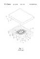
- FIG. 1shows a first level of packaging of a die package 40 in accordance with the prior art.
- a die (or integrated circuit) 20is attached to a lead frame 22 having a plurality of conductive leads 24 formed thereon.
- the die 20is typically attached with a layer of adhesive epoxy or glue. Bonding pads 26 on the die 20 are connected by bonding wires 28 to respective contact pads 30 on the lead frame 22 , a technique commonly known as wire-bonding.
- the contact pads 30are electrically coupled to an inner end of each conductive lead 24 .
- each conductive lead 24has an outer end that terminates in a connecting pin 32 .
- the die 20 and lead frame 22are then encapsulated by a cover 34 , thus constituting the first level of packaging.
- the encapsulated die and lead framemay be mounted to an electronics device, such as by inserting the connecting pins 32 into associated sockets on a printed circuit board and securing the pins in place using solder reflow techniques.
- FIG. 2shows the die 20 mounted directly to a circuit board 40 in a COB or “flip chip” packaging arrangement.
- the bonding pads 26are located on a bottom surface of the die 20 .
- the circuit board 40has a set of terminals or conductive bumps 42 on one surface.
- the die 20is mounted with the bonding pads 26 of the die 20 facing the surface of the printed circuit board 40 to which the die 20 is being mounted such that the bonding pads 26 make direct contact with the terminals 42 .
- the bonding wires 28 and lead frame 22are eliminated.
- a layer of materialknown as a glob top or encapsulating layer 44 over the die 20 to hermetically seal the die 20 .
- the glob top 44serves as a chemical insulator protecting the die 20 from humidity, oxidation, and other harmful elements.
- the glob top 44also protects the die 20 mechanically and relieves mechanical stress in the die 20 .
- FIG. 3shows a packaging arrangement having an inner die 50 mounted in a flip chip arrangement on the circuit board 40 such that the bonding pads 26 of the inner die 50 are in direct contact with the conductive terminals 42 on the circuit board 40 .
- An outer die 52is attached to the inner die 50 .
- Bonding wires 28extend from a set of second bonding pads 54 on the outer die 52 to a set of second terminals 56 on the circuit board 40 .
- a glob top 44is then applied over the stacked die to hermetically seal and protect the die 50 , 52 .
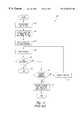
- FIG. 4shows a conventional method 60 of assembling and testing stacked die on a printed circuit board (PCB).
- a first step 62the inner die 50 is attached to the PCB 40 with the contact pads 26 of the inner die 50 in contact with the terminals 42 .
- the outer die 52is then attached to the inner die 50 in a second step 64 , and the glob top is applied to encapsulate the die in a third “sealing” step 65 .
- a fourth “testing” step 66input signals are systematically applied to the package to test all or some aspects of component performance, including speed, functionality, open circuits, shorts, and burn-in testing.
- a fifth “determination” step 68it is determined whether the package has performed the tests successfully. If so, the assembly and test method is complete 70 .
- the packageis determined whether the package has previously been reworked 72 . If the package has been previously reworked but continues to fail the tests, the entire package is discarded in a “rejection” step 74 , including the inner die, the outer die, and in some cases even the PCB. If the package has not been previously reworked, however, the package is reworked 76 , and the package is returned to the testing step 66 for evaluation.
- the glob top 44is designed to protect the die from environmental and mechanical stress, the materials used for the glob top are typically poor thermal conductors. Due to relatively poor heat dissipation through the glob top, the die or the PCB may become hotter than desirable, particularly for stacked die or high-power die applications.
- the conventional method of testing the die packageinvolves testing after the inner die has been attached to the PCB and the outer die has been attached to the inner die, if a package does not pass a test successfully, the stacked die and PCB package must undergo a time-consuming and costly rework procedure, or must be discarded entirely. This is particularly true if the testing is performed after the glob top has been applied.
- a stacked die packagecomprises a packaging substrate including a first surface having a recess disposed therein and a plurality of conductive leads coupled thereto, a first die attached to the packaging substrate within the recess and having a plurality of first bond pads, and a second die attached to the first die and having a plurality of second bond pads, the first and second bond pads being electrically coupled to at least some of the conductive leads.
- the first surface of the packaging substrateis proximate the circuit board so that the packaging substrate at least partially encloses and protects the first and second die.
- the properties and dimensions of the packaging substrateare tailored to optimize the operational environment of the die, including improving thermal dissipation and enhancing performance of the die.
- the packaging substratecomprises an electrically-conductive substrate and an electrically insulative layer is formed between the conductive leads and the packaging substrate.
- the first bond padsare electrically coupled to the conductive leads by wire-bonding. Alternately, the first bond pads are in direct contact with the conductive leads in a flip chip arrangement. In another aspect, the first and second die are sealed within an encapsulating layer for protection.
- a method of packaging and testing a die package in accordance with the inventionincludes testing a die having a plurality of bond pads formed thereon, determining that the die has tested successfully, providing a packaging substrate including a first surface having a recess formed therein and a plurality of conductive leads formed thereon, attaching the die to the packaging substrate within the recess and with the bond pads electrically coupled to at least some of the conductive leads to form the die package, and testing the die package.
- a method of packaging and testingincludes determining that the die package has not previously been reworked. Alternately, a method includes reworking the die package. In another alternate aspect, a method includes determining that the die package is salvageable. If so, the die package may be salvaged. Alternately, a method includes sealing the die in an encapsulating layer.
- An embodiment of a method of packaging and testing a stacked die package in accordance with the inventionincludes testing a first die having a plurality of first bond pads formed thereon, determining that the first die has tested successfully, testing a second die having a plurality of second bond pads formed thereon, determining that the second die has tested successfully, attaching the second die to the first die, providing a packaging substrate including a first surface having a recess formed therein and a plurality of conductive leads formed thereon, attaching the first die to the packaging substrate within the recess and with the first and second bond pads electrically coupled to at least some of the conductive leads to form the stacked die package, and testing the stacked die package.
- FIG. 1is an isometric partially exploded view of a die and a lead frame package in accordance with the prior art.
- FIG. 2is a side cross-sectional view of a chip on board package in accordance with the prior art.
- FIG. 3is a side cross-sectional view of a stacked die package in accordance with the prior art.
- FIG. 4is a flowchart representation of a method of packaging and testing of a stacked die package in accordance with the prior art.
- FIG. 5is a side cross-sectional view of a die package in accordance with an embodiment of the invention.
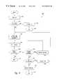
- FIG. 6is a flowchart representation of a method of packaging and testing of the die package of FIG. 5 in accordance with an embodiment of the invention.
- FIG. 7is a side cross-sectional view of a stacked die package in accordance with an alternate embodiment of the invention.
- FIG. 8is a flowchart representation of a method of packaging and testing of the stacked die package of FIG. 7 in accordance with an embodiment of the invention.
- FIG. 9is a side cross-sectional view of a stacked die package in accordance with another embodiment of the invention.
- FIG. 5is a side cross-sectional view of a die package 100 in accordance with an embodiment of the invention.
- the die package 100includes a packaging substrate 102 with a lower surface 104 having a recess 106 disposed therein.
- the packaging substrate 102 of the die package 100may be any suitable material, including a thermally conductive material, such as metal.
- a die 108 having a set of bond pads 110is disposed within the recess 106 and attached to the packaging substrate 102 .
- the die 108may be attached using a layer of adhesive epoxy or tape, or may be thermally-bonded (e.g. eutectically bonded), or may be attached by any other suitable attachment mechanism.
- a corresponding set of contact pads 112are attached to the packaging substrate 102 . In this embodiment, the contact pads 112 are located within the recess 106 .
- a bond wire 114electrically couples each bond pad 110 to a corresponding contact pad 112 using conventional wire-bonding methods.
- the bond padsmay be electrically coupled with the contact pads in a variety of ways, such as by tape automated bonding (TAB), microbump bonding, or flip chip bonding.
- TABtape automated bonding
- the die 108may be sealed within an encapsulating layer, such as the glob top 44 layer of the prior art die packages shown in FIGS. 2 and 3.
- a set of via 115are formed in the substrate 102 .
- Conductive leads 116are formed within the via 115 .
- An electrically insulative layer 117may be formed about each conductive lead 116 between the lead and the walls of the via 115 , electrically insulating the conductive lead 116 from the substrate 102 .
- Each conductive lead 116has an inner end proximate to the recess 106 coupled to a contact pad 112 .
- the inner ends of the conductive leads 116 being “proximate” the recess 106includes the condition where the conductive leads 116 are at least partially within the recess 106 , as shown in FIG. 5 .
- Each conductive lead 116also includes an outer end coupled to a ball pad 117 upon which may be formed a solder ball (or bump) 118 .
- the solder balls 118are then coupled with a corresponding set of terminals 122 of an electrical circuit (e.g. a printed circuit board 120 ) by any conventional method, such as, for example, by solder reflow techniques. Alternately, some other type of coupling device may be used instead of solder balls.
- the solder balls 118may be replaced with connecting pins (FIG. 1) that engage receptacles on the printed circuit board 120 .
- die packagesare described as being attached to the printed circuit board 120 . It is understood, however, that the die packages may be coupled with any number of suitable devices, including test carriers, other electronic components, die packages, or electrical circuits. To simplify the following discussion, however, the die packages will be described as being attached to or engageable with a printed circuit board, allowing the reader to focus on the inventive aspects of the packaging and testing of the die.
- the packaging substrate 102serves as both a lead frame and a protective cover for the die 108 .
- Two of the components of the conventional die package shown in FIG. 1are therefore combined into a single element (i.e., the packaging substrate 102 ) with an associated reduction in the cost of packaging the die.
- the packaging substrate 102may be a thermally conductive material, improved cooling characteristics are achieved over prior art die packages.
- the dimensions and thermal properties of the substrate 102may be tailored to the particular die 108 , or the anticipated operational characteristics thereof, in order to optimize the operational environment and extend the life of the die 108 .
- the dissipation of heat away from the die 108can be better regulated and controlled, particularly for high-power die applications.
- the electrically insulative layer 117may be formed about the conductive leads 116 to electrically insulate to prevent electrical shorts. If the packaging substrate 102 is not electrically conductive, the insulative layer 117 may be eliminated, and the conductive leads 116 may be formed in the via 115 in contact with the packaging substrate 102 .
- FIG. 6shows a method of packaging and testing 600 of the die package 100 of FIG. 5 in accordance with an embodiment of the invention.
- the die package 100undergoes an integrated process of testing and packaging.
- the die 108may be subjected to a battery of tests, such as speed, functionality, continuity, and burn-in tests.
- a battery of testssuch as speed, functionality, continuity, and burn-in tests.
- the dieis attached to the packaging substrate in an attachment step 656 .
- an abbreviated test 658is performed on the die package, including, for example, continuity testing. It is then determined whether the die package tested successfully 660 . If the die package tests successfully, the process of packaging and testing of the die is complete 661 .
- the die packagedoes not test successfully, it is determined whether the die package have already been reworked 662 . If not, the die package is reworked 664 , and the die package is returned for testing 658 . If the die package has already been reworked, however, it is determined whether the die is salvageable 666 . If the die is salvageable, it is salvaged by removing the die from the packaging substrate 668 , and the die is returned to the step of attaching the die to a packaging substrate 656 . The old packaging substrate may be re-attached and tested with a different die, or discarded. If the die is not salvageable, the die package is discarded 670 and the process of packaging the die is ended 672 .
- the method of packaging and testing 600 of the die packageadvantageously improves the efficiency of the packaging and testing by integrating testing steps into the packaging process. Because the die is initially tested independently from the packaging substrate, if the die fails a test, the labor involved in packaging the bad die is saved. Also, diagnostic interpretation of the test results is simplified because the test failure can be immediately associated with the bad die.
- the method 600improves the overall efficiency of the testing of the die package. Since the die has been subjected to a battery of die-related tests (speed, functionality, etc.) the complexity of the testing of the die package is substantially reduced. Test failures of the die package are therefore more easily and rapidly diagnosed as being associated with the attachment of the die with the packaging substrate. The amount of diagnostic work and die package reworking is reduced, and overall, the testing process is more efficient than the prior art method described above.
- FIG. 7is a side cross-sectional view of a stacked die package 200 in accordance with an alternate embodiment of the invention.
- the stacked die package 200is similar to the previously described embodiment except that a second (or outer) die 208 is attached to the first (or inner) die 108 and partially disposed within the recess 106 .
- the bond pads 110 of the first die 108are connected by first bond wires 114 to corresponding first contact pads 114 on the lower surface 104 of the substrate 102 .
- the first contact pads 112are not disposed within the recess 106 , but rather, are proximate the recess 106 on the lower surface 104 of the packaging substrate.
- the second die 208has a set of contact pads 210 that are electrically coupled by second bond wires 214 to a set of second contact pads 212 located on the lower surface 104 .
- An encapsulating layer 244encompasses the die, bond pads, and bond wires.
- Conductive leads 116connect each of the first and second contact pads 112 , 212 to corresponding solder balls 118 .
- the solder balls 118are then coupleable with terminals 122 on the printed circuit board 120 as described above.
- the stacked die package 200advantageously provides the improved thermal dissipation characteristics described above, as well as the recognized advantages of economical use of surface space on the printed board afforded by the stacking of the die.
- an electrically insulative layer 117may be formed between the conductive leads 116 and the lower surface 104 , as shown in FIG. 7 .
- the conductive leads 116may be mounted to the lower surface 104 on the electrically insulative layer 117 (FIG. 5) such as, for example, an insulative tape material using conventional tape automated bonding (TAB) techniques, to prevent electrical shorts.
- TABtape automated bonding
- some (or all) of the conductive leads 116may be disposed within via 115 formed within the packaging substrate 102 (as shown in FIG. 5 ), or for an electrically insulative packaging substrate 102 , the electrically insulative layer 117 may be eliminated.
- the encapsulating layer 244 of the stacked die package 200may be eliminated, the advantages of a hermetically sealed die may be realized in a die package in accordance with the invention that also offers improved thermal dissipation characteristics over prior art die packages. Because the die are attached to the packaging substrate which has a relatively large surface area facing away from the printed circuit board, improved thermal dissipation is achieved for die packages having single or multiple die that are protected by an encapsulating layer 244 .
- FIG. 8shows a method of packaging and testing 800 of the stacked die package 200 of FIG. 7 .
- the method 800begins by testing 850 of the first and second die.
- the testing of the individual dieis preferably rigorous and comprehensive.
- a determination step 852it is determined whether the first and second die tested successfully. If not, the unsuccessful die is discarded 854 , and the method returns to the die testing step 850 until both die are successfully tested.
- the first and second dieare attached together 855 .
- the first dieis then attached 856 to the packaging substrate within the recess 106 to form the stacked die package 200 .
- the first diemay be attached to the packaging substrate prior to the attachment of the first die to the second die.
- the stacked die packageis tested 858 .
- the testing of the stacked die package 858may be relatively simple.
- step 860it is determined whether the stacked die package has tested successfully. If the stacked die package passes the testing, an encapsulating layer may be applied 861 , and the method terminated successfully 863 . Alternately, the encapsulating layer may be omitted.
- the packagedoes not test successfully, however, a determination is made whether the package has already been reworked 862 . If the stacked die package has not previously been reworked, it is reworked 864 to correct the testing failures, such as, for example, by rewiring one or more of the first and second contact pads 110 , 210 with the first and second bond pads 112 , 212 respectively. The reworked die package is then returned for testing 858 .
- the die packagedoes not test successfully 860 and it has previously been reworked 862 , a determination is made whether the stacked die are salvageable 866 . If so, the stacked die are salvaged 868 and returned for attachment to a new packaging substrate 856 , and the subsequent acts are repeated. If the stacked die are not salvageable, however, the stacked die package is discarded 870 , and the method 800 is terminated 872 with an unsuccessful result.
- the method 800 shown in FIG. 8involves a greater number of acts than are shown in the prior art method 60 shown in FIG. 4, the method 800 is more economical. Individual testing of the die prior to attachment to the packaging substrate simplifies the subsequent testing of the stacked die package, and makes diagnosis of test failures easier. Also, the combination of individual die testing 850 and testing of the stacked die package 858 prior to attachment to the printed circuit board improves the yield of the packaging and testing process in comparison with the prior art method 60 . The method 800 reduces the effort involved in diagnosing test failures, the effort involved in reworking die packaging, and the waste and loss of production associated with discarding unsuccessful components.
- FIG. 9is a side cross-sectional view of a stacked die package 300 in accordance with another embodiment of the invention.
- the stacked die package 300is similar to the previously described stacked die package 200 , except that the first die 108 is coupled to the substrate 102 in a flip chip arrangement.
- the recess 106 in this embodimentis more shallow so that the second die 208 is not fully disposed within the recess 106 .
- the first contact pads 112are disposed within the recess 106 of the packaging substrate 102 , and the first bond pads 110 on the first die 108 are in direct contact with the first contact pads 112 on the substrate 102 .
- Conductive leads 116connect the first contact pads 112 with a set of solder bumps 118 .
- the second die 208is attached to the first die 108 , and the second bond pads 210 are wire-bonded to the second contact pads 212 on the lower surface 104 of the substrate 102 .
- Conductive leads 116also connect the second contact pads 112 with corresponding solder bumps 118 which, in turn, are engaged with the terminals 122 on the printed circuit board 120 .
- an electrically insulative layer 117may be formed between the conductive leads 116 and the lower surface 104 . Alternately, for an electrically insulative packaging substrate 102 , the electrically insulative layer 117 may be eliminated.
- the stacked die package 300may be packaged and tested in accordance with the methods described above and shown on FIG. 8 .
- the stacked die package 300advantageously provides the benefits of the inventive packaging arrangement, including improved thermal dissipation, physical protection, and elimination of components as described above, together with the benefits of flip chip packaging. Because the first lead wires 114 between the first bond pads 110 and the first contact pads 112 are eliminated, the electrical contact between the first die and the packaging substrate is more reliable, and the speed of the first chip is improved.
- the depth of the recess 106may be adjusted to any desired depth in accordance with the requirements of the die package. For example, for some stacked die combinations, it may be desirable to increase the depth of the recess to situate both the first and second die within the recess. Alternately, for other applications a shallow recess may be preferred. Where a shallow recess is used, it may be necessary to increase the size of the solder bumps (or connecting pins) to increase the distance between the printed circuit board and the packaging substrate to prevent the second die 208 or the second bond wires 214 from contacting the printed circuit board 120 . An encapsulating layer (see FIG. 7) may also be added to hermetically seal and protect the die, bond pads, contact pads, and bond wires.
Landscapes
- Engineering & Computer Science (AREA)
- Microelectronics & Electronic Packaging (AREA)
- Power Engineering (AREA)
- Computer Hardware Design (AREA)
- Physics & Mathematics (AREA)
- Condensed Matter Physics & Semiconductors (AREA)
- General Physics & Mathematics (AREA)
- Manufacturing & Machinery (AREA)
- Encapsulation Of And Coatings For Semiconductor Or Solid State Devices (AREA)
- Tests Of Electronic Circuits (AREA)
- Testing Of Individual Semiconductor Devices (AREA)
- Structures Or Materials For Encapsulating Or Coating Semiconductor Devices Or Solid State Devices (AREA)
Abstract
Description
Claims (16)
Priority Applications (4)
| Application Number | Priority Date | Filing Date | Title |
|---|---|---|---|
| US09/385,766US6294839B1 (en) | 1999-08-30 | 1999-08-30 | Apparatus and methods of packaging and testing die |
| US09/851,657US6558966B2 (en) | 1999-08-30 | 2001-05-08 | Apparatus and methods of packaging and testing die |
| US09/872,221US6380631B2 (en) | 1999-08-30 | 2001-05-31 | Apparatus and methods of packaging and testing die |
| US09/941,317US6512302B2 (en) | 1999-08-30 | 2001-08-28 | Apparatus and methods of packaging and testing die |
Applications Claiming Priority (1)
| Application Number | Priority Date | Filing Date | Title |
|---|---|---|---|
| US09/385,766US6294839B1 (en) | 1999-08-30 | 1999-08-30 | Apparatus and methods of packaging and testing die |
Related Child Applications (3)
| Application Number | Title | Priority Date | Filing Date |
|---|---|---|---|
| US09/851,657DivisionUS6558966B2 (en) | 1999-08-30 | 2001-05-08 | Apparatus and methods of packaging and testing die |
| US09/872,221DivisionUS6380631B2 (en) | 1999-08-30 | 2001-05-31 | Apparatus and methods of packaging and testing die |
| US09/941,317ContinuationUS6512302B2 (en) | 1999-08-30 | 2001-08-28 | Apparatus and methods of packaging and testing die |
Publications (1)
| Publication Number | Publication Date |
|---|---|
| US6294839B1true US6294839B1 (en) | 2001-09-25 |
Family
ID=23522792
Family Applications (4)
| Application Number | Title | Priority Date | Filing Date |
|---|---|---|---|
| US09/385,766Expired - LifetimeUS6294839B1 (en) | 1999-08-30 | 1999-08-30 | Apparatus and methods of packaging and testing die |
| US09/851,657Expired - LifetimeUS6558966B2 (en) | 1999-08-30 | 2001-05-08 | Apparatus and methods of packaging and testing die |
| US09/872,221Expired - LifetimeUS6380631B2 (en) | 1999-08-30 | 2001-05-31 | Apparatus and methods of packaging and testing die |
| US09/941,317Expired - LifetimeUS6512302B2 (en) | 1999-08-30 | 2001-08-28 | Apparatus and methods of packaging and testing die |
Family Applications After (3)
| Application Number | Title | Priority Date | Filing Date |
|---|---|---|---|
| US09/851,657Expired - LifetimeUS6558966B2 (en) | 1999-08-30 | 2001-05-08 | Apparatus and methods of packaging and testing die |
| US09/872,221Expired - LifetimeUS6380631B2 (en) | 1999-08-30 | 2001-05-31 | Apparatus and methods of packaging and testing die |
| US09/941,317Expired - LifetimeUS6512302B2 (en) | 1999-08-30 | 2001-08-28 | Apparatus and methods of packaging and testing die |
Country Status (1)
| Country | Link |
|---|---|
| US (4) | US6294839B1 (en) |
Cited By (106)
| Publication number | Priority date | Publication date | Assignee | Title |
|---|---|---|---|---|
| US6404648B1 (en)* | 2001-03-30 | 2002-06-11 | Hewlett-Packard Co. | Assembly and method for constructing a multi-die integrated circuit |
| US6479759B2 (en)* | 2000-07-19 | 2002-11-12 | Alcatel | Submount, electronic assembly and process for producing the same |
| US20030042581A1 (en)* | 2001-08-29 | 2003-03-06 | Fee Setho Sing | Packaged microelectronic devices and methods of forming same |
| US6548326B2 (en)* | 1999-06-21 | 2003-04-15 | Shinko Electronic Industries Co., Ltd. | Semiconductor device and process of producing same |
| US6548376B2 (en) | 2001-08-30 | 2003-04-15 | Micron Technology, Inc. | Methods of thinning microelectronic workpieces |
| US20030071341A1 (en)* | 2001-10-16 | 2003-04-17 | Jeung Boon Suan | Apparatus and method for leadless packaging of semiconductor devices |
| US6552910B1 (en) | 2000-06-28 | 2003-04-22 | Micron Technology, Inc. | Stacked-die assemblies with a plurality of microelectronic devices and methods of manufacture |
| US6559528B2 (en)* | 2000-02-21 | 2003-05-06 | Matsushita Electric Industrial Co., Ltd. | Semiconductor device and method for the fabrication thereof |
| US6558600B1 (en) | 2000-05-04 | 2003-05-06 | Micron Technology, Inc. | Method for packaging microelectronic substrates |
| US6560117B2 (en) | 2000-06-28 | 2003-05-06 | Micron Technology, Inc. | Packaged microelectronic die assemblies and methods of manufacture |
| US6564979B2 (en) | 2001-07-18 | 2003-05-20 | Micron Technology, Inc. | Method and apparatus for dispensing adhesive on microelectronic substrate supports |
| US6576494B1 (en) | 2000-06-28 | 2003-06-10 | Micron Technology, Inc. | Recessed encapsulated microelectronic devices and methods for formation |
| US6600221B2 (en)* | 2000-08-31 | 2003-07-29 | Nec Electronics Corporation | Semiconductor device with stacked semiconductor chips |
| US20030148597A1 (en)* | 2002-01-09 | 2003-08-07 | Tan Hock Chuan | Stacked die in die BGA package |
| US6607937B1 (en) | 2000-08-23 | 2003-08-19 | Micron Technology, Inc. | Stacked microelectronic dies and methods for stacking microelectronic dies |
| US6622380B1 (en) | 2002-02-12 | 2003-09-23 | Micron Technology, Inc. | Methods for manufacturing microelectronic devices and methods for mounting microelectronic packages to circuit boards |
| US6638595B2 (en) | 2000-06-28 | 2003-10-28 | Micron Technology, Inc. | Method and apparatus for reduced flash encapsulation of microelectronic devices |
| US6653173B2 (en) | 2000-06-16 | 2003-11-25 | Micron Technology, Inc. | Method and apparatus for packaging a microelectronic die |
| US6656769B2 (en) | 2000-05-08 | 2003-12-02 | Micron Technology, Inc. | Method and apparatus for distributing mold material in a mold for packaging microelectronic devices |
| US20040019841A1 (en)* | 2002-07-25 | 2004-01-29 | Ong Adrian E. | Internally generating patterns for testing in an integrated circuit device |
| US20040029425A1 (en)* | 2002-08-06 | 2004-02-12 | Yean Tay Wuu | Temporary, conformable contacts for microelectronic components |
| US20040026776A1 (en)* | 2002-08-08 | 2004-02-12 | Brand Joseph M. | Microelectronic devices and methods for manufacturing and operating packaged microelectronic device assemblies |
| US20040031621A1 (en)* | 2002-08-19 | 2004-02-19 | Heng Puah Kia | Packaged microelectronic component assemblies |
| US20040036490A1 (en)* | 2002-08-26 | 2004-02-26 | Ralph Schaeffer | Selectively configurable probe structures, e.g., for testing microelectronic components |
| US20040038447A1 (en)* | 2002-08-21 | 2004-02-26 | Corisis David J | Packaged microelectronic devices and methods for assembling microelectronic devices |
| US20040040149A1 (en)* | 2002-08-29 | 2004-03-04 | Wood Alan G. | Probe card , e.g., for testing microelectronic components, and methods for making same |
| US6732304B1 (en) | 2000-09-21 | 2004-05-04 | Inapac Technology, Inc. | Chip testing within a multi-chip semiconductor package |
| US20040095736A1 (en)* | 2002-11-18 | 2004-05-20 | Samsung Electronics Co., Ltd. | Multi-chip package having increased reliabilty |
| US20040100772A1 (en)* | 2002-11-22 | 2004-05-27 | Chye Lim Thiam | Packaged microelectronic component assemblies |
| US6750547B2 (en) | 2001-12-26 | 2004-06-15 | Micron Technology, Inc. | Multi-substrate microelectronic packages and methods for manufacture |
| US20040113251A1 (en)* | 2002-12-16 | 2004-06-17 | Tan Say Leong | Semiconductor chip package with a package substrate and a lid cover |
| US6754866B1 (en) | 2001-09-28 | 2004-06-22 | Inapac Technology, Inc. | Testing of integrated circuit devices |
| US20040155331A1 (en)* | 2003-02-11 | 2004-08-12 | Blaine Thurgood | Packaged microelectronic devices and methods for packaging microelectronic devices |
| US20040173899A1 (en)* | 2003-03-04 | 2004-09-09 | Peng Neo Chee | Microelectronic component assemblies employing lead frames having reduced-thickness inner lengths |
| US20040178495A1 (en)* | 2003-03-14 | 2004-09-16 | Yean Tay Wuu | Microelectronic devices and methods for packaging microelectronic devices |
| US6796028B2 (en) | 2000-08-23 | 2004-09-28 | Micron Technology, Inc. | Method of Interconnecting substrates for electrical coupling of microelectronic components |
| US6812726B1 (en) | 2002-11-27 | 2004-11-02 | Inapac Technology, Inc. | Entering test mode and accessing of a packaged semiconductor device |
| US20040232523A1 (en)* | 2003-04-30 | 2004-11-25 | Khosro Shamsaifar | Electronically tunable RF chip packages |
| US6836009B2 (en) | 2002-08-08 | 2004-12-28 | Micron Technology, Inc. | Packaged microelectronic components |
| US6838760B1 (en) | 2000-08-28 | 2005-01-04 | Micron Technology, Inc. | Packaged microelectronic devices with interconnecting units |
| US20050019988A1 (en)* | 2002-04-04 | 2005-01-27 | Tongbi Jiang | Method and apparatus for attaching microelectronic substrates and support members |
| US20050019984A1 (en)* | 2000-08-09 | 2005-01-27 | Tongbi Jiang | Multiple substrate microelectronic devices and methods of manufacture |
| US20050024977A1 (en)* | 2000-09-21 | 2005-02-03 | Ong Adrian E. | Multiple power levels for a chip within a multi-chip semiconductor package |
| US20050026415A1 (en)* | 2002-01-16 | 2005-02-03 | Micron Technology, Inc. | Fabrication of stacked microelectronic devices |
| US20050045378A1 (en)* | 2003-08-29 | 2005-03-03 | Heng Mung Suan | Stacked microfeature devices and associated methods |
| US20050046431A1 (en)* | 2003-09-03 | 2005-03-03 | Kirby Kyle K. | Probe card for use with microelectronic components,and methods for making same |
| US6866470B2 (en) | 1999-10-19 | 2005-03-15 | Micron Technology, Inc. | Methods and apparatus for retaining a tray stack having a plurality of trays for carrying microelectronic devices |
| US20050093174A1 (en)* | 2003-10-31 | 2005-05-05 | Seng Eric T.S. | Reduced footprint packaged microelectronic components and methods for manufacturing such microelectronic components |
| US20050104171A1 (en)* | 2003-11-13 | 2005-05-19 | Benson Peter A. | Microelectronic devices having conductive complementary structures and methods of manufacturing microelectronic devices having conductive complementary structures |
| US20050104228A1 (en)* | 2003-11-13 | 2005-05-19 | Rigg Sidney B. | Microelectronic devices, methods for forming vias in microelectronic devices, and methods for packaging microelectronic devices |
| US20050127478A1 (en)* | 2003-12-10 | 2005-06-16 | Hiatt William M. | Microelectronic devices and methods for filling vias in microelectronic devices |
| US20050134299A1 (en)* | 2003-12-22 | 2005-06-23 | Cram Daniel P. | System and apparatus for testing packaged devices and related methods |
| US6921860B2 (en) | 2003-03-18 | 2005-07-26 | Micron Technology, Inc. | Microelectronic component assemblies having exposed contacts |
| US20050162182A1 (en)* | 2002-07-25 | 2005-07-28 | Ong Adrian E. | Internally generating patterns for testing in an integrated circuit device |
| US20050189140A1 (en)* | 2004-02-26 | 2005-09-01 | Chao-Ming Tseng | Chip package structure |
| US20050206401A1 (en)* | 2004-03-22 | 2005-09-22 | Caldwell John L | Test sockets, test systems, and methods for testing microfeature devices |
| US20050277279A1 (en)* | 2004-06-14 | 2005-12-15 | Shijian Luo | Microfeature devices and methods for manufacturing microfeature devices |
| US6979595B1 (en) | 2000-08-24 | 2005-12-27 | Micron Technology, Inc. | Packaged microelectronic devices with pressure release elements and methods for manufacturing and using such packaged microelectronic devices |
| US20050289428A1 (en)* | 2000-09-21 | 2005-12-29 | Sidley Austin Brown & Wood Llp | Architecture and method for testing of an integrated circuit device |
| US20060017177A1 (en)* | 2004-07-23 | 2006-01-26 | Seng Eric T S | Microelectronic component assemblies with recessed wire bonds and methods of making same |
| US20060038274A1 (en)* | 2004-08-20 | 2006-02-23 | Masahiro Ono | 3D circuit module, multilayer 3D circuit module formed thereof, mobile terminal device using the circuit modules and method for manufacturing the circuit modules |
| US20060046346A1 (en)* | 2004-09-01 | 2006-03-02 | Benson Peter A | Methods for packaging microfeature devices and microfeature devices formed by such methods |
| US20060044773A1 (en)* | 2004-08-25 | 2006-03-02 | Micron Technology, Inc. | Methods and apparatuses for transferring heat from stacked microfeature devices |
| US20060068523A1 (en)* | 2003-05-20 | 2006-03-30 | Infineon Technologies Ag | Integrated circuit package |
| US7037756B1 (en) | 2001-08-30 | 2006-05-02 | Micron Technology, Inc. | Stacked microelectronic devices and methods of fabricating same |
| US7061263B1 (en) | 2001-11-15 | 2006-06-13 | Inapac Technology, Inc. | Layout and use of bond pads and probe pads for testing of integrated circuits devices |
| US20060292858A1 (en)* | 2002-07-18 | 2006-12-28 | Micron Technology, Inc. | Techniques to create low K ILD for beol |
| US20070031998A1 (en)* | 2000-08-16 | 2007-02-08 | Micron Technology, Inc. | Method and apparatus for removing encapsulating material from a packaged microelectronic device |
| US20070045803A1 (en)* | 2005-08-26 | 2007-03-01 | Micron Technology, Inc. | Microelectronic device packages, stacked microelectronic device packages, and methods for manufacturing microelectronic devices |
| US20070045872A1 (en)* | 2005-08-31 | 2007-03-01 | Fee Setho S | Microelectronic devices having intermediate contacts for connection to interposer substrates, and associated methods of packaging microelectronic devices with intermediate contacts |
| US20070045796A1 (en)* | 2005-08-19 | 2007-03-01 | Micron Technology, Inc. | Microelectronic devices, stacked microelectronic devices, and methods for manufacturing microelectronic devices |
| US20070045807A1 (en)* | 2005-09-01 | 2007-03-01 | Micron Technology, Inc. | Microelectronic devices and methods for manufacturing microelectronic devices |
| US20070045862A1 (en)* | 2005-09-01 | 2007-03-01 | Micron Technology, Inc. | Stacked microelectronic devices and methods for manufacturing microelectronic devices |
| US20070045797A1 (en)* | 2005-08-24 | 2007-03-01 | Micron Technology, Inc. | Microelectronic devices and microelectronic support devices, and associated assemblies and methods |
| US7198693B1 (en) | 2002-02-20 | 2007-04-03 | Micron Technology, Inc. | Microelectronic device having a plurality of stacked dies and methods for manufacturing such microelectronic assemblies |
| US20070079204A1 (en)* | 2001-09-28 | 2007-04-05 | Ong Adrian E | Integrated Circuit Testing Module Including Signal Shaping Interface |
| US20070148820A1 (en)* | 2005-12-22 | 2007-06-28 | Micron Technology, Inc. | Microelectronic devices and methods for manufacturing microelectronic devices |
| US20070155048A1 (en)* | 2005-12-29 | 2007-07-05 | Micron Technology, Inc. | Methods for packaging microelectronic devices and microelectronic devices formed using such methods |
| US7259451B2 (en) | 2003-08-29 | 2007-08-21 | Micron Technology, Inc. | Invertible microfeature device packages |
| US20070210441A1 (en)* | 2006-03-08 | 2007-09-13 | Micron Technology, Inc. | Microelectronic device assemblies including assemblies with recurved leadframes, and associated methods |
| US20070228577A1 (en)* | 2006-03-29 | 2007-10-04 | Micron Technology, Inc. | Packaged microelectronic devices recessed in support member cavities, and associated methods |
| US20080012110A1 (en)* | 2006-07-17 | 2008-01-17 | Micron Technology, Inc. | Microelectronic packages with leadframes, including leadframes configured for stacked die packages, and associated systems and methods |
| US20080048316A1 (en)* | 2006-08-25 | 2008-02-28 | Micron Technology, Inc. | Packaged microdevices and methods for manufacturing packaged microdevices |
| US20080128900A1 (en)* | 2006-12-04 | 2008-06-05 | Micron Technology, Inc. | Packaged microelectronic devices and methods for manufacturing packaged microelectronic devices |
| US20080224291A1 (en)* | 2007-03-13 | 2008-09-18 | Micron Technology, Inc. | Packaged semiconductor components having substantially rigid support members and methods of packaging semiconductor components |
| US20080224329A1 (en)* | 2007-03-13 | 2008-09-18 | Micron Technology, Inc. | Packaged microelectronic devices and methods for manufacturing packaged microelectronic devices |
| US7466603B2 (en) | 2006-10-03 | 2008-12-16 | Inapac Technology, Inc. | Memory accessing circuit system |
| US20090045489A1 (en)* | 2007-08-16 | 2009-02-19 | Micron Technology, Inc. | Microelectronic die packages with leadframes, including leadframe-based interposer for stacked die packages, and associated systems and methods |
| US7518237B2 (en) | 2005-02-08 | 2009-04-14 | Micron Technology, Inc. | Microfeature systems including adhered microfeature workpieces and support members |
| US20090273359A1 (en)* | 2008-05-02 | 2009-11-05 | Micron Technology, Inc. | Electrical testing apparatus having masked sockets and associated systems and methods |
| US7671459B2 (en) | 2006-02-08 | 2010-03-02 | Micron Technologies, Inc. | Microelectronic devices, stacked microelectronic devices, and methods for manufacturing such devices |
| US7807505B2 (en) | 2005-08-30 | 2010-10-05 | Micron Technology, Inc. | Methods for wafer-level packaging of microfeature devices and microfeature devices formed using such methods |
| US7833456B2 (en) | 2007-02-23 | 2010-11-16 | Micron Technology, Inc. | Systems and methods for compressing an encapsulant adjacent a semiconductor workpiece |
| US7843050B2 (en) | 2007-07-24 | 2010-11-30 | Micron Technology, Inc. | Microelectronic die packages with metal leads, including metal leads for stacked die packages, and associated systems and methods |
| SG167661A1 (en)* | 2002-01-09 | 2011-01-28 | Micron Technology Inc | Stacked die in die bga package |
| US7910385B2 (en) | 2006-05-12 | 2011-03-22 | Micron Technology, Inc. | Method of fabricating microelectronic devices |
| US8063650B2 (en) | 2002-11-27 | 2011-11-22 | Rambus Inc. | Testing fuse configurations in semiconductor devices |
| EP1876644A3 (en)* | 2006-06-30 | 2012-01-25 | Fujitsu Semiconductor Limited | Semiconductor device and manufacturing method of same |
| US8166361B2 (en) | 2001-09-28 | 2012-04-24 | Rambus Inc. | Integrated circuit testing module configured for set-up and hold time testing |
| US8286046B2 (en) | 2001-09-28 | 2012-10-09 | Rambus Inc. | Integrated circuit testing module including signal shaping interface |
| US20140345929A1 (en)* | 2011-12-20 | 2014-11-27 | Kyocera Corporation | Electronic component housing package and electronic apparatus |
| USD728577S1 (en)* | 2014-07-01 | 2015-05-05 | Google Inc. | Mobile device module |
| USD730906S1 (en)* | 2014-07-01 | 2015-06-02 | Google Inc. | Mobile device module |
| US9165888B2 (en) | 2008-09-11 | 2015-10-20 | Micron Technology, Inc. | Interconnect structures for stacked dies, including penetrating structures for through-silicon vias, and associated systems and methods |
| US20170207182A1 (en)* | 2016-01-19 | 2017-07-20 | Xintec Inc. | Chip package and method for forming the same |
| US20180108542A1 (en)* | 2009-09-23 | 2018-04-19 | STATS ChipPAC Pte. Ltd. | Semiconductor Device and Method of Forming Interposer with Opening to Contain Semiconductor Die |
Families Citing this family (52)
| Publication number | Priority date | Publication date | Assignee | Title |
|---|---|---|---|---|
| EP1189280A4 (en)* | 2000-03-29 | 2005-03-02 | Rohm Co Ltd | Semiconductor device |
| AU2002217987A1 (en) | 2000-12-01 | 2002-06-11 | Broadcom Corporation | Thermally and electrically enhanced ball grid array packaging |
| US20020079572A1 (en)* | 2000-12-22 | 2002-06-27 | Khan Reza-Ur Rahman | Enhanced die-up ball grid array and method for making the same |
| US7161239B2 (en) | 2000-12-22 | 2007-01-09 | Broadcom Corporation | Ball grid array package enhanced with a thermal and electrical connector |
| US6906414B2 (en) | 2000-12-22 | 2005-06-14 | Broadcom Corporation | Ball grid array package with patterned stiffener layer |
| US7132744B2 (en) | 2000-12-22 | 2006-11-07 | Broadcom Corporation | Enhanced die-up ball grid array packages and method for making the same |
| US7259448B2 (en)* | 2001-05-07 | 2007-08-21 | Broadcom Corporation | Die-up ball grid array package with a heat spreader and method for making the same |
| TW502406B (en)* | 2001-08-01 | 2002-09-11 | Siliconware Precision Industries Co Ltd | Ultra-thin package having stacked die |
| KR20030018642A (en)* | 2001-08-30 | 2003-03-06 | 주식회사 하이닉스반도체 | Stack chip module |
| US6879039B2 (en)* | 2001-12-18 | 2005-04-12 | Broadcom Corporation | Ball grid array package substrates and method of making the same |
| US7550845B2 (en)* | 2002-02-01 | 2009-06-23 | Broadcom Corporation | Ball grid array package with separated stiffener layer |
| US6861750B2 (en) | 2002-02-01 | 2005-03-01 | Broadcom Corporation | Ball grid array package with multiple interposers |
| US6825108B2 (en) | 2002-02-01 | 2004-11-30 | Broadcom Corporation | Ball grid array package fabrication with IC die support structures |
| US6876553B2 (en) | 2002-03-21 | 2005-04-05 | Broadcom Corporation | Enhanced die-up ball grid array package with two substrates |
| US7196415B2 (en) | 2002-03-22 | 2007-03-27 | Broadcom Corporation | Low voltage drop and high thermal performance ball grid array package |
| US6791168B1 (en)* | 2002-07-10 | 2004-09-14 | Micron Technology, Inc. | Semiconductor package with circuit side polymer layer and wafer level fabrication method |
| KR100664796B1 (en)* | 2002-12-30 | 2007-01-04 | 동부일렉트로닉스 주식회사 | Side braze package |
| US20040135242A1 (en)* | 2003-01-09 | 2004-07-15 | Hsin Chung Hsien | Stacked structure of chips |
| JP4110992B2 (en)* | 2003-02-07 | 2008-07-02 | セイコーエプソン株式会社 | Semiconductor device, electronic device, electronic apparatus, semiconductor device manufacturing method, and electronic device manufacturing method |
| US7239024B2 (en)* | 2003-04-04 | 2007-07-03 | Thomas Joel Massingill | Semiconductor package with recess for die |
| US6917090B2 (en)* | 2003-04-07 | 2005-07-12 | Micron Technology, Inc. | Chip scale image sensor package |
| US7116557B1 (en)* | 2003-05-23 | 2006-10-03 | Sti Electronics, Inc. | Imbedded component integrated circuit assembly and method of making same |
| JP4161267B2 (en)* | 2003-08-06 | 2008-10-08 | セイコーエプソン株式会社 | Surface acoustic wave device |
| US6982491B1 (en)* | 2004-01-20 | 2006-01-03 | Asat Ltd. | Sensor semiconductor package and method of manufacturing the same |
| US20050248028A1 (en)* | 2004-05-05 | 2005-11-10 | Cheng-Yen Huang | Chip-packaging with bonding options connected to a package substrate |
| US7411281B2 (en) | 2004-06-21 | 2008-08-12 | Broadcom Corporation | Integrated circuit device package having both wire bond and flip-chip interconnections and method of making the same |
| US7432586B2 (en)* | 2004-06-21 | 2008-10-07 | Broadcom Corporation | Apparatus and method for thermal and electromagnetic interference (EMI) shielding enhancement in die-up array packages |
| US7482686B2 (en) | 2004-06-21 | 2009-01-27 | Braodcom Corporation | Multipiece apparatus for thermal and electromagnetic interference (EMI) shielding enhancement in die-up array packages and method of making the same |
| JP4601365B2 (en)* | 2004-09-21 | 2010-12-22 | ルネサスエレクトロニクス株式会社 | Semiconductor device |
| US7786591B2 (en) | 2004-09-29 | 2010-08-31 | Broadcom Corporation | Die down ball grid array package |
| TW200612345A (en)* | 2004-10-07 | 2006-04-16 | Advanced Flash Memory Card Technology Co Ltd | Structure of memory card and producing method thereof |
| US20060175694A1 (en)* | 2005-02-07 | 2006-08-10 | Hsin Chung H | Stacked structure of integrated circuits and method for manufacturing the same |
| US20070051949A1 (en)* | 2005-09-06 | 2007-03-08 | Peter Schneider | Method and arrangment for testing a stacked die semiconductor device |
| US7224278B2 (en)* | 2005-10-18 | 2007-05-29 | Avery Dennison Corporation | Label with electronic components and method of making same |
| US20070152696A1 (en)* | 2006-01-03 | 2007-07-05 | Ross Larry K | Water bond-out |
| US20070252260A1 (en)* | 2006-04-28 | 2007-11-01 | Micron Technology, Inc. | Stacked die packages |
| US8183680B2 (en) | 2006-05-16 | 2012-05-22 | Broadcom Corporation | No-lead IC packages having integrated heat spreader for electromagnetic interference (EMI) shielding and thermal enhancement |
| US7888185B2 (en)* | 2006-08-17 | 2011-02-15 | Micron Technology, Inc. | Semiconductor device assemblies and systems including at least one conductive pathway extending around a side of at least one semiconductor device |
| US7701352B2 (en)* | 2006-11-22 | 2010-04-20 | Avery Dennison Corporation | RFID label with release liner window, and method of making |
| DE102007023666A1 (en)* | 2006-12-01 | 2008-06-05 | Infineon Technologies Ag | Semiconductor component e.g. silicon chip, has passivation layer extended on contact distributor layer and comprising opening that is arranged on section of contact distributor layer, and connection contact arranged on opening |
| JP5579402B2 (en)* | 2009-04-13 | 2014-08-27 | ピーエスフォー ルクスコ エスエイアールエル | Semiconductor device, method for manufacturing the same, and electronic device |
| US8093714B2 (en)* | 2009-12-10 | 2012-01-10 | Semtech Corporation | Chip assembly with chip-scale packaging |
| KR20110088234A (en)* | 2010-01-28 | 2011-08-03 | 삼성전자주식회사 | Manufacturing method of laminated semiconductor package |
| US8357564B2 (en)* | 2010-05-17 | 2013-01-22 | Stats Chippac, Ltd. | Semiconductor device and method of forming prefabricated multi-die leadframe for electrical interconnect of stacked semiconductor die |
| US8598695B2 (en) | 2010-07-23 | 2013-12-03 | Tessera, Inc. | Active chip on carrier or laminated chip having microelectronic element embedded therein |
| US9337116B2 (en)* | 2010-10-28 | 2016-05-10 | Stats Chippac, Ltd. | Semiconductor device and method of forming stepped interposer for stacking and electrically connecting semiconductor die |
| US8797057B2 (en)* | 2011-02-11 | 2014-08-05 | Taiwan Semiconductor Manufacturing Company, Ltd. | Testing of semiconductor chips with microbumps |
| DE102011086722A1 (en)* | 2011-11-21 | 2013-05-23 | Robert Bosch Gmbh | Micromechanical functional device, in particular speaker device, and corresponding manufacturing method |
| US9799627B2 (en)* | 2012-01-19 | 2017-10-24 | Semiconductor Components Industries, Llc | Semiconductor package structure and method |
| TWI517341B (en)* | 2013-05-10 | 2016-01-11 | 矽品精密工業股份有限公司 | Semiconductor package and method of manufacture |
| US11195740B2 (en)* | 2019-04-17 | 2021-12-07 | Micron Technology, Inc. | Methods and apparatus for wafer handling and processing |
| CN115064531A (en)* | 2022-08-18 | 2022-09-16 | 艾科微电子(深圳)有限公司 | Converter, electronic device, and converter packaging method |
Citations (21)
| Publication number | Priority date | Publication date | Assignee | Title |
|---|---|---|---|---|
| US5088190A (en) | 1990-08-30 | 1992-02-18 | Texas Instruments Incorporated | Method of forming an apparatus for burn in testing of integrated circuit chip |
| EP0231937B1 (en) | 1986-02-06 | 1993-12-08 | Hitachi Maxell Ltd. | An arrangement of a semiconductor device for use in a card |
| EP0595549A2 (en) | 1992-10-26 | 1994-05-04 | Hughes Microelectronics Europa Limited | Radio frequency baggage tags |
| US5528222A (en) | 1994-09-09 | 1996-06-18 | International Business Machines Corporation | Radio frequency circuit and memory in thin flexible package |
| US5541525A (en) | 1991-06-04 | 1996-07-30 | Micron Technology, Inc. | Carrier for testing an unpackaged semiconductor die |
| US5566441A (en) | 1993-03-11 | 1996-10-22 | British Technology Group Limited | Attaching an electronic circuit to a substrate |
| US5600175A (en) | 1994-07-27 | 1997-02-04 | Texas Instruments Incorporated | Apparatus and method for flat circuit assembly |
| US5607818A (en) | 1991-06-04 | 1997-03-04 | Micron Technology, Inc. | Method for making interconnects and semiconductor structures using electrophoretic photoresist deposition |
| US5633122A (en) | 1993-08-16 | 1997-05-27 | Micron Technology, Inc. | Test fixture and method for producing a test fixture for testing unpackaged semiconductor die |
| US5634267A (en) | 1991-06-04 | 1997-06-03 | Micron Technology, Inc. | Method and apparatus for manufacturing known good semiconductor die |
| US5656551A (en) | 1994-11-14 | 1997-08-12 | Micron Technology, Inc. | Method for attaching a semiconductor die to a support |
| US5682143A (en) | 1994-09-09 | 1997-10-28 | International Business Machines Corporation | Radio frequency identification tag |
| US5733800A (en) | 1996-05-21 | 1998-03-31 | Micron Technology, Inc. | Underfill coating for LOC package |
| US5767564A (en)* | 1993-10-19 | 1998-06-16 | Kyocera Corporation | Semiconductor device with a decoupling capacitor mounted thereon having a thermal expansion coefficient matched to the device |
| US5784260A (en) | 1996-05-29 | 1998-07-21 | International Business Machines Corporation | Structure for constraining the flow of encapsulant applied to an I/C chip on a substrate |
| US5811879A (en) | 1996-06-26 | 1998-09-22 | Micron Technology, Inc. | Stacked leads-over-chip multi-chip module |
| US5818698A (en) | 1995-10-12 | 1998-10-06 | Micron Technology, Inc. | Method and apparatus for a chip-on-board semiconductor module |
| US5875100A (en) | 1996-05-31 | 1999-02-23 | Nec Corporation | High-density mounting method and structure for electronic circuit board |
| US5898217A (en) | 1998-01-05 | 1999-04-27 | Motorola, Inc. | Semiconductor device including a substrate having clustered interconnects |
| US5963429A (en)* | 1997-08-20 | 1999-10-05 | Sulzer Intermedics Inc. | Printed circuit substrate with cavities for encapsulating integrated circuits |
| JP2000252787A (en)* | 1998-12-28 | 2000-09-14 | Toshiba Corp | Surface acoustic wave device and envelope for surface acoustic wave device |
Family Cites Families (9)
| Publication number | Priority date | Publication date | Assignee | Title |
|---|---|---|---|---|
| DE3578224D1 (en) | 1984-07-27 | 1990-07-19 | Fujitsu Ltd | INTEGRATED CHIP-TO-CHIP TYPE. |
| US4985988A (en)* | 1989-11-03 | 1991-01-22 | Motorola, Inc. | Method for assembling, testing, and packaging integrated circuits |
| US5155067A (en)* | 1991-03-26 | 1992-10-13 | Micron Technology, Inc. | Packaging for a semiconductor die |
| US5291062A (en) | 1993-03-01 | 1994-03-01 | Motorola, Inc. | Area array semiconductor device having a lid with functional contacts |
| US5701233A (en)* | 1995-01-23 | 1997-12-23 | Irvine Sensors Corporation | Stackable modules and multimodular assemblies |
| TW373308B (en) | 1995-02-24 | 1999-11-01 | Agere Systems Inc | Thin packaging of multi-chip modules with enhanced thermal/power management |
| US5633530A (en) | 1995-10-24 | 1997-05-27 | United Microelectronics Corporation | Multichip module having a multi-level configuration |
| US5710695A (en)* | 1995-11-07 | 1998-01-20 | Vlsi Technology, Inc. | Leadframe ball grid array package |
| US6057598A (en)* | 1997-01-31 | 2000-05-02 | Vlsi Technology, Inc. | Face on face flip chip integration |
- 1999
- 1999-08-30USUS09/385,766patent/US6294839B1/ennot_activeExpired - Lifetime
- 2001
- 2001-05-08USUS09/851,657patent/US6558966B2/ennot_activeExpired - Lifetime
- 2001-05-31USUS09/872,221patent/US6380631B2/ennot_activeExpired - Lifetime
- 2001-08-28USUS09/941,317patent/US6512302B2/ennot_activeExpired - Lifetime
Patent Citations (21)
| Publication number | Priority date | Publication date | Assignee | Title |
|---|---|---|---|---|
| EP0231937B1 (en) | 1986-02-06 | 1993-12-08 | Hitachi Maxell Ltd. | An arrangement of a semiconductor device for use in a card |
| US5088190A (en) | 1990-08-30 | 1992-02-18 | Texas Instruments Incorporated | Method of forming an apparatus for burn in testing of integrated circuit chip |
| US5541525A (en) | 1991-06-04 | 1996-07-30 | Micron Technology, Inc. | Carrier for testing an unpackaged semiconductor die |
| US5607818A (en) | 1991-06-04 | 1997-03-04 | Micron Technology, Inc. | Method for making interconnects and semiconductor structures using electrophoretic photoresist deposition |
| US5634267A (en) | 1991-06-04 | 1997-06-03 | Micron Technology, Inc. | Method and apparatus for manufacturing known good semiconductor die |
| EP0595549A2 (en) | 1992-10-26 | 1994-05-04 | Hughes Microelectronics Europa Limited | Radio frequency baggage tags |
| US5566441A (en) | 1993-03-11 | 1996-10-22 | British Technology Group Limited | Attaching an electronic circuit to a substrate |
| US5633122A (en) | 1993-08-16 | 1997-05-27 | Micron Technology, Inc. | Test fixture and method for producing a test fixture for testing unpackaged semiconductor die |
| US5767564A (en)* | 1993-10-19 | 1998-06-16 | Kyocera Corporation | Semiconductor device with a decoupling capacitor mounted thereon having a thermal expansion coefficient matched to the device |
| US5600175A (en) | 1994-07-27 | 1997-02-04 | Texas Instruments Incorporated | Apparatus and method for flat circuit assembly |
| US5528222A (en) | 1994-09-09 | 1996-06-18 | International Business Machines Corporation | Radio frequency circuit and memory in thin flexible package |
| US5682143A (en) | 1994-09-09 | 1997-10-28 | International Business Machines Corporation | Radio frequency identification tag |
| US5656551A (en) | 1994-11-14 | 1997-08-12 | Micron Technology, Inc. | Method for attaching a semiconductor die to a support |
| US5818698A (en) | 1995-10-12 | 1998-10-06 | Micron Technology, Inc. | Method and apparatus for a chip-on-board semiconductor module |
| US5733800A (en) | 1996-05-21 | 1998-03-31 | Micron Technology, Inc. | Underfill coating for LOC package |
| US5784260A (en) | 1996-05-29 | 1998-07-21 | International Business Machines Corporation | Structure for constraining the flow of encapsulant applied to an I/C chip on a substrate |
| US5875100A (en) | 1996-05-31 | 1999-02-23 | Nec Corporation | High-density mounting method and structure for electronic circuit board |
| US5811879A (en) | 1996-06-26 | 1998-09-22 | Micron Technology, Inc. | Stacked leads-over-chip multi-chip module |
| US5963429A (en)* | 1997-08-20 | 1999-10-05 | Sulzer Intermedics Inc. | Printed circuit substrate with cavities for encapsulating integrated circuits |
| US5898217A (en) | 1998-01-05 | 1999-04-27 | Motorola, Inc. | Semiconductor device including a substrate having clustered interconnects |
| JP2000252787A (en)* | 1998-12-28 | 2000-09-14 | Toshiba Corp | Surface acoustic wave device and envelope for surface acoustic wave device |
Cited By (352)
| Publication number | Priority date | Publication date | Assignee | Title |
|---|---|---|---|---|
| US6548326B2 (en)* | 1999-06-21 | 2003-04-15 | Shinko Electronic Industries Co., Ltd. | Semiconductor device and process of producing same |
| US7086562B2 (en) | 1999-10-19 | 2006-08-08 | Micron Technology, Inc. | Methods and apparatus for retaining a tray stack having a plurality of trays for carrying microelectronic devices |
| US7066708B1 (en) | 1999-10-19 | 2006-06-27 | Micron Technology, Inc. | Methods and apparatus for retaining a tray stack having a plurality of trays for carrying microelectric devices |
| US6866470B2 (en) | 1999-10-19 | 2005-03-15 | Micron Technology, Inc. | Methods and apparatus for retaining a tray stack having a plurality of trays for carrying microelectronic devices |
| US6559528B2 (en)* | 2000-02-21 | 2003-05-06 | Matsushita Electric Industrial Co., Ltd. | Semiconductor device and method for the fabrication thereof |
| US6924173B2 (en) | 2000-02-21 | 2005-08-02 | Matsushita Electric Industrial Co., Ltd. | Semiconductor device and method for the fabrication thereof |
| US20030194834A1 (en)* | 2000-02-21 | 2003-10-16 | Matsushita Electric Industrial Co., Ltd. | Semiconductor device and method for the fabrication thereof |
| US6558600B1 (en) | 2000-05-04 | 2003-05-06 | Micron Technology, Inc. | Method for packaging microelectronic substrates |
| US20030209831A1 (en)* | 2000-05-04 | 2003-11-13 | Williams Vernon M. | Method and apparatus for packaging microelectronic substrates |
| US6656769B2 (en) | 2000-05-08 | 2003-12-02 | Micron Technology, Inc. | Method and apparatus for distributing mold material in a mold for packaging microelectronic devices |
| US6677675B2 (en) | 2000-06-16 | 2004-01-13 | Micron Technology, Inc. | Microelectronic devices and microelectronic die packages |
| US6664139B2 (en) | 2000-06-16 | 2003-12-16 | Micron Technology, Inc. | Method and apparatus for packaging a microelectronic die |
| US6653173B2 (en) | 2000-06-16 | 2003-11-25 | Micron Technology, Inc. | Method and apparatus for packaging a microelectronic die |
| US6683388B2 (en) | 2000-06-16 | 2004-01-27 | Micron Technology, Inc. | Method and apparatus for packaging a microelectronic die |
| US6841423B2 (en) | 2000-06-28 | 2005-01-11 | Micron Technology, Inc. | Methods for formation of recessed encapsulated microelectronic devices |
| US6644949B2 (en) | 2000-06-28 | 2003-11-11 | Micron Technology, Inc. | Apparatus for reduced flash encapsulation of microelectronic devices |
| US6819003B2 (en) | 2000-06-28 | 2004-11-16 | Micron Technology Inc. | Recessed encapsulated microelectronic devices and methods for formation |
| US6552910B1 (en) | 2000-06-28 | 2003-04-22 | Micron Technology, Inc. | Stacked-die assemblies with a plurality of microelectronic devices and methods of manufacture |
| US6576494B1 (en) | 2000-06-28 | 2003-06-10 | Micron Technology, Inc. | Recessed encapsulated microelectronic devices and methods for formation |
| US6560117B2 (en) | 2000-06-28 | 2003-05-06 | Micron Technology, Inc. | Packaged microelectronic die assemblies and methods of manufacture |
| US6638595B2 (en) | 2000-06-28 | 2003-10-28 | Micron Technology, Inc. | Method and apparatus for reduced flash encapsulation of microelectronic devices |
| US6479759B2 (en)* | 2000-07-19 | 2002-11-12 | Alcatel | Submount, electronic assembly and process for producing the same |
| US7253025B2 (en) | 2000-08-09 | 2007-08-07 | Micron Technology, Inc. | Multiple substrate microelectronic devices and methods of manufacture |
| US20050019984A1 (en)* | 2000-08-09 | 2005-01-27 | Tongbi Jiang | Multiple substrate microelectronic devices and methods of manufacture |
| US7298031B1 (en)* | 2000-08-09 | 2007-11-20 | Micron Technology, Inc. | Multiple substrate microelectronic devices and methods of manufacture |
| US20070031998A1 (en)* | 2000-08-16 | 2007-02-08 | Micron Technology, Inc. | Method and apparatus for removing encapsulating material from a packaged microelectronic device |
| US7405487B2 (en) | 2000-08-16 | 2008-07-29 | Micron Technology, Inc. | Method and apparatus for removing encapsulating material from a packaged microelectronic device |
| US7273769B1 (en) | 2000-08-16 | 2007-09-25 | Micron Technology, Inc. | Method and apparatus for removing encapsulating material from a packaged microelectronic device |
| US6982386B2 (en) | 2000-08-23 | 2006-01-03 | Micron Technology, Inc. | Interconnecting substrates for electrical coupling of microelectronic components |
| US6983551B2 (en) | 2000-08-23 | 2006-01-10 | Micron Technology, Inc. | Interconnecting substrates for electrical coupling of microelectronic components |
| US6796028B2 (en) | 2000-08-23 | 2004-09-28 | Micron Technology, Inc. | Method of Interconnecting substrates for electrical coupling of microelectronic components |
| US6607937B1 (en) | 2000-08-23 | 2003-08-19 | Micron Technology, Inc. | Stacked microelectronic dies and methods for stacking microelectronic dies |
| US20070210435A1 (en)* | 2000-08-23 | 2007-09-13 | Micron Technology, Inc. | Stacked microelectronic dies and methods for stacking microelectronic dies |
| US8587109B2 (en) | 2000-08-23 | 2013-11-19 | Micron Technology, Inc. | Stacked microelectronic dies and methods for stacking microelectronic dies |
| US20040038449A1 (en)* | 2000-08-23 | 2004-02-26 | Corisis David J. | Stacked microelectronic dies and methods for stacking microelectronic dies |
| US8067827B2 (en) | 2000-08-23 | 2011-11-29 | Micron Technology, Inc. | Stacked microelectronic device assemblies |
| US7235871B2 (en) | 2000-08-23 | 2007-06-26 | Micron Technology, Inc. | Stacked microelectronic dies |
| US7049685B2 (en) | 2000-08-24 | 2006-05-23 | Micron Technology, Inc. | Packaged microelectronic devices with pressure release elements and methods for manufacturing and using such packaged microelectronic devices |
| US6979595B1 (en) | 2000-08-24 | 2005-12-27 | Micron Technology, Inc. | Packaged microelectronic devices with pressure release elements and methods for manufacturing and using such packaged microelectronic devices |
| US6838760B1 (en) | 2000-08-28 | 2005-01-04 | Micron Technology, Inc. | Packaged microelectronic devices with interconnecting units |
| US7332376B2 (en) | 2000-08-28 | 2008-02-19 | Micron Technology, Inc. | Method of encapsulating packaged microelectronic devices with a barrier |
| US7101737B2 (en) | 2000-08-28 | 2006-09-05 | Micron Technology, Inc. | Method of encapsulating interconnecting units in packaged microelectronic devices |
| US6600221B2 (en)* | 2000-08-31 | 2003-07-29 | Nec Electronics Corporation | Semiconductor device with stacked semiconductor chips |
| US7444575B2 (en) | 2000-09-21 | 2008-10-28 | Inapac Technology, Inc. | Architecture and method for testing of an integrated circuit device |
| US7139945B2 (en) | 2000-09-21 | 2006-11-21 | Inapac Technology, Inc. | Chip testing within a multi-chip semiconductor package |
| US20050289428A1 (en)* | 2000-09-21 | 2005-12-29 | Sidley Austin Brown & Wood Llp | Architecture and method for testing of an integrated circuit device |
| US20040196709A1 (en)* | 2000-09-21 | 2004-10-07 | Ong Adrian E. | Chip testing within a multi-chip semiconductor package |
| US20050024977A1 (en)* | 2000-09-21 | 2005-02-03 | Ong Adrian E. | Multiple power levels for a chip within a multi-chip semiconductor package |
| US7240254B2 (en) | 2000-09-21 | 2007-07-03 | Inapac Technology, Inc | Multiple power levels for a chip within a multi-chip semiconductor package |
| US6732304B1 (en) | 2000-09-21 | 2004-05-04 | Inapac Technology, Inc. | Chip testing within a multi-chip semiconductor package |
| US6404648B1 (en)* | 2001-03-30 | 2002-06-11 | Hewlett-Packard Co. | Assembly and method for constructing a multi-die integrated circuit |
| US6564979B2 (en) | 2001-07-18 | 2003-05-20 | Micron Technology, Inc. | Method and apparatus for dispensing adhesive on microelectronic substrate supports |
| US20030042581A1 (en)* | 2001-08-29 | 2003-03-06 | Fee Setho Sing | Packaged microelectronic devices and methods of forming same |
| US6876066B2 (en) | 2001-08-29 | 2005-04-05 | Micron Technology, Inc. | Packaged microelectronic devices and methods of forming same |
| US6943450B2 (en) | 2001-08-29 | 2005-09-13 | Micron Technology, Inc. | Packaged microelectronic devices and methods of forming same |
| US20050023655A1 (en)* | 2001-08-29 | 2005-02-03 | Fee Setho Sing | Packaged microelectronic devices and methods of forming same |
| US6548376B2 (en) | 2001-08-30 | 2003-04-15 | Micron Technology, Inc. | Methods of thinning microelectronic workpieces |
| US7037756B1 (en) | 2001-08-30 | 2006-05-02 | Micron Technology, Inc. | Stacked microelectronic devices and methods of fabricating same |
| US20040225937A1 (en)* | 2001-09-28 | 2004-11-11 | Ong Adrian E. | Testing of integrated circuit devices |
| US10114073B2 (en) | 2001-09-28 | 2018-10-30 | Rambus Inc. | Integrated circuit testing |
| US8001439B2 (en) | 2001-09-28 | 2011-08-16 | Rambus Inc. | Integrated circuit testing module including signal shaping interface |
| US6754866B1 (en) | 2001-09-28 | 2004-06-22 | Inapac Technology, Inc. | Testing of integrated circuit devices |
| US9116210B2 (en) | 2001-09-28 | 2015-08-25 | Rambus Inc. | Integrated circuit testing module including signal shaping interface |
| US8286046B2 (en) | 2001-09-28 | 2012-10-09 | Rambus Inc. | Integrated circuit testing module including signal shaping interface |
| US20070079204A1 (en)* | 2001-09-28 | 2007-04-05 | Ong Adrian E | Integrated Circuit Testing Module Including Signal Shaping Interface |
| US8166361B2 (en) | 2001-09-28 | 2012-04-24 | Rambus Inc. | Integrated circuit testing module configured for set-up and hold time testing |
| US7103815B2 (en) | 2001-09-28 | 2006-09-05 | Inapac Technology, Inc. | Testing of integrated circuit devices |
| US6747348B2 (en) | 2001-10-16 | 2004-06-08 | Micron Technology, Inc. | Apparatus and method for leadless packaging of semiconductor devices |
| US20030080403A1 (en)* | 2001-10-16 | 2003-05-01 | Jeung Boon Suan | Apparatus and method for leadless packaging of semiconductor devices |
| US20030071338A1 (en)* | 2001-10-16 | 2003-04-17 | Jeung Boon Suan | Apparatus and method for leadless packaging of semiconductor devices |
| US6790706B2 (en) | 2001-10-16 | 2004-09-14 | Micron Technology, Inc. | Apparatus and method for leadless packaging of semiconductor devices |
| US20030071341A1 (en)* | 2001-10-16 | 2003-04-17 | Jeung Boon Suan | Apparatus and method for leadless packaging of semiconductor devices |
| US6787894B2 (en) | 2001-10-16 | 2004-09-07 | Micron Technology, Inc. | Apparatus and method for leadless packaging of semiconductor devices |
| US6743696B2 (en) | 2001-10-16 | 2004-06-01 | Micron Technology, Inc. | Apparatus and method for leadless packaging of semiconductor devices |
| US7061263B1 (en) | 2001-11-15 | 2006-06-13 | Inapac Technology, Inc. | Layout and use of bond pads and probe pads for testing of integrated circuits devices |
| US6841418B2 (en) | 2001-12-26 | 2005-01-11 | Micron Technology, Inc. | Multi-substrate microelectronic packages and methods for manufacture |
| US20040183207A1 (en)* | 2001-12-26 | 2004-09-23 | Jeung Boon Suan | Multi-substrate microelectronic packages and methods for manufacture |
| US6750547B2 (en) | 2001-12-26 | 2004-06-15 | Micron Technology, Inc. | Multi-substrate microelectronic packages and methods for manufacture |
| US7358117B2 (en) | 2002-01-09 | 2008-04-15 | Micron Technology, Inc. | Stacked die in die BGA package |
| US7282390B2 (en) | 2002-01-09 | 2007-10-16 | Micron Technology, Inc. | Stacked die-in-die BGA package with die having a recess |
| US7332820B2 (en) | 2002-01-09 | 2008-02-19 | Micron Technology, Inc. | Stacked die in die BGA package |
| US20030148597A1 (en)* | 2002-01-09 | 2003-08-07 | Tan Hock Chuan | Stacked die in die BGA package |
| US20060292743A1 (en)* | 2002-01-09 | 2006-12-28 | Micron Technolgoy, Inc. | Stacked die in die BGA package |
| US7332819B2 (en) | 2002-01-09 | 2008-02-19 | Micron Technology, Inc. | Stacked die in die BGA package |
| US20080032449A1 (en)* | 2002-01-09 | 2008-02-07 | Micron Technology, Inc. | Stacked Die in Die BGA Package |
| US20060292746A1 (en)* | 2002-01-09 | 2006-12-28 | Micron Technology, Inc. | Stacked die in die BGA package |
| US20060292745A1 (en)* | 2002-01-09 | 2006-12-28 | Micron Technology, Inc. | Stacked die in die BGA package |
| US8373277B2 (en) | 2002-01-09 | 2013-02-12 | Micron Technology, Inc. | Stacked die in die BGA package |
| US7309623B2 (en) | 2002-01-09 | 2007-12-18 | Micron Technology, Inc. | Method of fabricating a stacked die in die BGA package |
| US20030162325A1 (en)* | 2002-01-09 | 2003-08-28 | Micron Technology, Inc. | Stacked die in die BGA package |
| US20060216864A1 (en)* | 2002-01-09 | 2006-09-28 | Micron Technology, Inc. | Stacked die in die BGA package |
| US20080136045A1 (en)* | 2002-01-09 | 2008-06-12 | Micron Technology, Inc. | Stacked die in die BGA package |
| SG167661A1 (en)* | 2002-01-09 | 2011-01-28 | Micron Technology Inc | Stacked die in die bga package |
| US7575953B2 (en) | 2002-01-09 | 2009-08-18 | Micron Technology, Inc. | Stacked die with a recess in a die BGA package |
| US7371608B2 (en) | 2002-01-09 | 2008-05-13 | Micron Technology, Inc. | Method of fabricating a stacked die having a recess in a die BGA package |
| US20080096316A1 (en)* | 2002-01-09 | 2008-04-24 | Micron Technology, Inc. | Stacked Die in Die BGA Package |
| US7799610B2 (en) | 2002-01-09 | 2010-09-21 | Micron Technology, Inc. | Method of fabricating a stacked die having a recess in a die BGA package |
| US7282392B2 (en) | 2002-01-09 | 2007-10-16 | Micron Technology, Inc. | Method of fabricating a stacked die in die BGA package |
| US7344969B2 (en)* | 2002-01-09 | 2008-03-18 | Micron Technology, Inc. | Stacked die in die BGA package |
| US20050026395A1 (en)* | 2002-01-16 | 2005-02-03 | Micron Technology, Inc. | Fabrication of stacked microelectronic devices |
| US20050026415A1 (en)* | 2002-01-16 | 2005-02-03 | Micron Technology, Inc. | Fabrication of stacked microelectronic devices |
| US7037751B2 (en) | 2002-01-16 | 2006-05-02 | Micron Technology, Inc. | Fabrication of stacked microelectronic devices |
| US6896760B1 (en) | 2002-01-16 | 2005-05-24 | Micron Technology, Inc. | Fabrication of stacked microelectronic devices |
| US7022418B2 (en) | 2002-01-16 | 2006-04-04 | Micron Technology, Inc. | Fabrication of stacked microelectronic devices |
| US20060159947A1 (en)* | 2002-01-16 | 2006-07-20 | Micron Technology, Inc. | Fabrication of stacked microelectronic devices |
| US20060172510A1 (en)* | 2002-01-16 | 2006-08-03 | Micron Technology, Inc. | Fabrication of stacked microelectronic devices |
| US7122905B2 (en) | 2002-02-12 | 2006-10-17 | Micron Technology, Inc. | Microelectronic devices and methods for mounting microelectronic packages to circuit boards |
| US6622380B1 (en) | 2002-02-12 | 2003-09-23 | Micron Technology, Inc. | Methods for manufacturing microelectronic devices and methods for mounting microelectronic packages to circuit boards |
| US7198693B1 (en) | 2002-02-20 | 2007-04-03 | Micron Technology, Inc. | Microelectronic device having a plurality of stacked dies and methods for manufacturing such microelectronic assemblies |
| US20050019988A1 (en)* | 2002-04-04 | 2005-01-27 | Tongbi Jiang | Method and apparatus for attaching microelectronic substrates and support members |
| US7615871B2 (en) | 2002-04-04 | 2009-11-10 | Micron Technology, Inc. | Method and apparatus for attaching microelectronic substrates and support members |
| US7109588B2 (en) | 2002-04-04 | 2006-09-19 | Micron Technology, Inc. | Method and apparatus for attaching microelectronic substrates and support members |
| US7091064B2 (en) | 2002-04-04 | 2006-08-15 | Micron Technology, Inc. | Method and apparatus for attaching microelectronic substrates and support members |
| US20060292858A1 (en)* | 2002-07-18 | 2006-12-28 | Micron Technology, Inc. | Techniques to create low K ILD for beol |
| US20040019841A1 (en)* | 2002-07-25 | 2004-01-29 | Ong Adrian E. | Internally generating patterns for testing in an integrated circuit device |
| US7313740B2 (en) | 2002-07-25 | 2007-12-25 | Inapac Technology, Inc. | Internally generating patterns for testing in an integrated circuit device |
| US20050162182A1 (en)* | 2002-07-25 | 2005-07-28 | Ong Adrian E. | Internally generating patterns for testing in an integrated circuit device |
| US20040029425A1 (en)* | 2002-08-06 | 2004-02-12 | Yean Tay Wuu | Temporary, conformable contacts for microelectronic components |
| US6913476B2 (en) | 2002-08-06 | 2005-07-05 | Micron Technology, Inc. | Temporary, conformable contacts for microelectronic components |
| US6836009B2 (en) | 2002-08-08 | 2004-12-28 | Micron Technology, Inc. | Packaged microelectronic components |
| US9418872B2 (en) | 2002-08-08 | 2016-08-16 | Micron Technology, Inc. | Packaged microelectronic components |
| US20060040422A1 (en)* | 2002-08-08 | 2006-02-23 | Micron Technology, Inc. | Microelectronic devices and methods for manufacturing and operating packaged microelectronic device |
| US7306974B2 (en) | 2002-08-08 | 2007-12-11 | Micron Technology, Inc. | Microelectronic devices and methods for manufacturing and operating packaged microelectronic device assemblies |
| US8637973B2 (en) | 2002-08-08 | 2014-01-28 | Micron Technology, Inc. | Packaged microelectronic components with terminals exposed through encapsulant |
| US7195957B2 (en) | 2002-08-08 | 2007-03-27 | Micron Technology, Inc. | Packaged microelectronic components |
| US20050026325A1 (en)* | 2002-08-08 | 2005-02-03 | Koon Eng Meow | Packaged microelectronic components |
| US20080067642A1 (en)* | 2002-08-08 | 2008-03-20 | Micron Technology, Inc. | Packaged microelectronic components |
| US7067905B2 (en) | 2002-08-08 | 2006-06-27 | Micron Technology, Inc. | Packaged microelectronic devices including first and second casings |
| US20040026776A1 (en)* | 2002-08-08 | 2004-02-12 | Brand Joseph M. | Microelectronic devices and methods for manufacturing and operating packaged microelectronic device assemblies |
| US6781066B2 (en) | 2002-08-19 | 2004-08-24 | Micron Technology, Inc. | Packaged microelectronic component assemblies |
| US6933170B2 (en) | 2002-08-19 | 2005-08-23 | Micron Technology, Inc. | Packaged microelectronic component assemblies |
| US20040031621A1 (en)* | 2002-08-19 | 2004-02-19 | Heng Puah Kia | Packaged microelectronic component assemblies |
| US20040191964A1 (en)* | 2002-08-19 | 2004-09-30 | Heng Puah Kia | Packaged microelectronic component assemblies |
| US20040188820A1 (en)* | 2002-08-21 | 2004-09-30 | Corisis David J | Packaged microelectronic devices and methods for assembling microelectronic devices |
| US6924550B2 (en) | 2002-08-21 | 2005-08-02 | Micron Technology, Inc. | Packaged microelectronic devices and methods for assembling microelectronic devices |
| US20040038447A1 (en)* | 2002-08-21 | 2004-02-26 | Corisis David J | Packaged microelectronic devices and methods for assembling microelectronic devices |
| US6740546B2 (en) | 2002-08-21 | 2004-05-25 | Micron Technology, Inc. | Packaged microelectronic devices and methods for assembling microelectronic devices |
| US7170304B2 (en) | 2002-08-26 | 2007-01-30 | Micron Technology, Inc. | Selectively configurable probe structures, e.g., selectively configurable probe cards for testing microelectronic components |
| US20050258848A1 (en)* | 2002-08-26 | 2005-11-24 | Ralph Schaeffer | Selectively configurable probe strucutres, e.g., for testing microelectronic components |
| US20050024072A1 (en)* | 2002-08-26 | 2005-02-03 | Ralph Schaeffer | Selectively configurable probe structures, e.g., for testing microelectronic components |
| US20050206399A1 (en)* | 2002-08-26 | 2005-09-22 | Micron Technology, Inc. | Selectively configurable probe structures, e.g., for testing microelectronic components |
| US20050024071A1 (en)* | 2002-08-26 | 2005-02-03 | Ralph Schaeffer | Selectively configurable probe structures, e.g., for testing microelectronic components |
| US20040036490A1 (en)* | 2002-08-26 | 2004-02-26 | Ralph Schaeffer | Selectively configurable probe structures, e.g., for testing microelectronic components |
| US6952109B2 (en) | 2002-08-26 | 2005-10-04 | Micron Technology, Inc. | Selectively configurable probe structures, e.g., for testing microelectronic components |
| US7145355B2 (en) | 2002-08-26 | 2006-12-05 | Micron Technology, Inc. | Selectively configurable probe structures, e.g., for testing microelectronic components |
| US6924653B2 (en) | 2002-08-26 | 2005-08-02 | Micron Technology, Inc. | Selectively configurable microelectronic probes |
| US6972580B2 (en) | 2002-08-26 | 2005-12-06 | Micron Technology, Inc. | Selectively configurable probe structures, e.g., for testing microelectronic components |
| US20040040149A1 (en)* | 2002-08-29 | 2004-03-04 | Wood Alan G. | Probe card , e.g., for testing microelectronic components, and methods for making same |
| US6773938B2 (en) | 2002-08-29 | 2004-08-10 | Micron Technology, Inc. | Probe card, e.g., for testing microelectronic components, and methods for making same |
| US20040113644A1 (en)* | 2002-08-29 | 2004-06-17 | Wood Alan G. | Probe card, e.g., for testing microelectronic components, and methods for making same |
| US6881974B2 (en) | 2002-08-29 | 2005-04-19 | Micron Technology, Inc. | Probe card for testing microelectronic components |
| US20040095736A1 (en)* | 2002-11-18 | 2004-05-20 | Samsung Electronics Co., Ltd. | Multi-chip package having increased reliabilty |
| US6951982B2 (en) | 2002-11-22 | 2005-10-04 | Micron Technology, Inc. | Packaged microelectronic component assemblies |
| US20040100772A1 (en)* | 2002-11-22 | 2004-05-27 | Chye Lim Thiam | Packaged microelectronic component assemblies |
| US9568544B2 (en) | 2002-11-27 | 2017-02-14 | Rambus Inc. | Testing fuse configurations in semiconductor devices |
| US8717052B2 (en) | 2002-11-27 | 2014-05-06 | Rambus Inc. | Testing fuse configurations in semiconductor devices |
| US10302696B2 (en) | 2002-11-27 | 2019-05-28 | Rambus Inc. | Testing fuse configurations in semiconductor devices |
| US7259582B2 (en) | 2002-11-27 | 2007-08-21 | Inapac Technology, Inc. | Bonding pads for testing of a semiconductor device |
| US11009548B2 (en) | 2002-11-27 | 2021-05-18 | Rambus Inc. | Testing fuse configurations in semiconductor devices |
| US8063650B2 (en) | 2002-11-27 | 2011-11-22 | Rambus Inc. | Testing fuse configurations in semiconductor devices |
| US20050204223A1 (en)* | 2002-11-27 | 2005-09-15 | Ong Adrian E. | Bonding pads for testing of a semiconductor device |
| US6882171B2 (en) | 2002-11-27 | 2005-04-19 | Inapac Technology, Inc. | Bonding pads for testing of a semiconductor device |
| US6812726B1 (en) | 2002-11-27 | 2004-11-02 | Inapac Technology, Inc. | Entering test mode and accessing of a packaged semiconductor device |
| US7400036B2 (en)* | 2002-12-16 | 2008-07-15 | Avago Technologies General Ip Pte Ltd | Semiconductor chip package with a package substrate and a lid cover |
| US20040113251A1 (en)* | 2002-12-16 | 2004-06-17 | Tan Say Leong | Semiconductor chip package with a package substrate and a lid cover |
| US6879050B2 (en) | 2003-02-11 | 2005-04-12 | Micron Technology, Inc. | Packaged microelectronic devices and methods for packaging microelectronic devices |
| US20040155331A1 (en)* | 2003-02-11 | 2004-08-12 | Blaine Thurgood | Packaged microelectronic devices and methods for packaging microelectronic devices |
| US20040173899A1 (en)* | 2003-03-04 | 2004-09-09 | Peng Neo Chee | Microelectronic component assemblies employing lead frames having reduced-thickness inner lengths |
| US7691680B2 (en) | 2003-03-04 | 2010-04-06 | Micron Technologies, Inc. | Method of fabricating microelectronic component assemblies employing lead frames having reduced-thickness inner lengths |
| US7057281B2 (en) | 2003-03-04 | 2006-06-06 | Micron Technology Inc. | Microelectronic component assemblies employing lead frames having reduced-thickness inner lengths |
| US7425470B2 (en) | 2003-03-04 | 2008-09-16 | Micron Technology, Inc. | Microelectronic component assemblies employing lead frames having reduced-thickness inner lengths |
| US6946325B2 (en) | 2003-03-14 | 2005-09-20 | Micron Technology, Inc. | Methods for packaging microelectronic devices |
| US7145228B2 (en) | 2003-03-14 | 2006-12-05 | Micron Technology, Inc. | Microelectronic devices |
| US7754531B2 (en) | 2003-03-14 | 2010-07-13 | Micron Technology, Inc. | Method for packaging microelectronic devices |
| US20060006534A1 (en)* | 2003-03-14 | 2006-01-12 | Yean Tay W | Microelectronic devices and methods for packaging microelectronic devices |
| US20040178495A1 (en)* | 2003-03-14 | 2004-09-16 | Yean Tay Wuu | Microelectronic devices and methods for packaging microelectronic devices |
| US20070128737A1 (en)* | 2003-03-14 | 2007-06-07 | Micron Technology, Inc. | Microelectronic devices and methods for packaging microelectronic devices |
| US6921860B2 (en) | 2003-03-18 | 2005-07-26 | Micron Technology, Inc. | Microelectronic component assemblies having exposed contacts |
| US20040232523A1 (en)* | 2003-04-30 | 2004-11-25 | Khosro Shamsaifar | Electronically tunable RF chip packages |
| WO2004100222A3 (en)* | 2003-04-30 | 2005-06-02 | Paratek Microwave Inc | Electronically tunable rf chip packages |
| US7727799B2 (en)* | 2003-05-20 | 2010-06-01 | Infineon Technologies Ag | Integrated circuit package |
| US20100207267A1 (en)* | 2003-05-20 | 2010-08-19 | Tiang Hock Lin | Integrated Circuit Package |
| US8102041B2 (en) | 2003-05-20 | 2012-01-24 | Infineon Technologies Ag | Integrated circuit package |
| US20060068523A1 (en)* | 2003-05-20 | 2006-03-30 | Infineon Technologies Ag | Integrated circuit package |
| US7259451B2 (en) | 2003-08-29 | 2007-08-21 | Micron Technology, Inc. | Invertible microfeature device packages |
| US9515046B2 (en) | 2003-08-29 | 2016-12-06 | Micron Technology, Inc. | Stacked microfeature devices and associated methods |
| US8400780B2 (en) | 2003-08-29 | 2013-03-19 | Micron Technology, Inc. | Stacked microfeature devices |
| US20100258939A1 (en)* | 2003-08-29 | 2010-10-14 | Micron Technology, Inc. | Stacked microfeature devices and associated methods |
| US11373979B2 (en) | 2003-08-29 | 2022-06-28 | Micron Technology, Inc. | Stacked microfeature devices and associated methods |
| US7071421B2 (en) | 2003-08-29 | 2006-07-04 | Micron Technology, Inc. | Stacked microfeature devices and associated methods |
| US11887970B2 (en) | 2003-08-29 | 2024-01-30 | Micron Technology, Inc. | Stacked microfeature devices and associated methods |
| US10062667B2 (en) | 2003-08-29 | 2018-08-28 | Micron Technology, Inc. | Stacked microfeature devices and associated methods |
| US7368810B2 (en) | 2003-08-29 | 2008-05-06 | Micron Technology, Inc. | Invertible microfeature device packages |
| US7742313B2 (en) | 2003-08-29 | 2010-06-22 | Micron Technology, Inc. | Stacked microfeature devices |
| US20050045378A1 (en)* | 2003-08-29 | 2005-03-03 | Heng Mung Suan | Stacked microfeature devices and associated methods |
| US20050046431A1 (en)* | 2003-09-03 | 2005-03-03 | Kirby Kyle K. | Probe card for use with microelectronic components,and methods for making same |
| US6924655B2 (en) | 2003-09-03 | 2005-08-02 | Micron Technology, Inc. | Probe card for use with microelectronic components, and methods for making same |
| US7691726B2 (en) | 2003-10-31 | 2010-04-06 | Micron Technology, Inc. | Reduced footprint packaged microelectronic components and methods for manufacturing such microelectronic components |
| US7218001B2 (en) | 2003-10-31 | 2007-05-15 | Micron Technology, Inc. | Reduced footprint packaged microelectronic components and methods for manufacturing such microelectronic components |
| US20050093174A1 (en)* | 2003-10-31 | 2005-05-05 | Seng Eric T.S. | Reduced footprint packaged microelectronic components and methods for manufacturing such microelectronic components |
| US9653420B2 (en) | 2003-11-13 | 2017-05-16 | Micron Technology, Inc. | Microelectronic devices and methods for filling vias in microelectronic devices |
| US20050104171A1 (en)* | 2003-11-13 | 2005-05-19 | Benson Peter A. | Microelectronic devices having conductive complementary structures and methods of manufacturing microelectronic devices having conductive complementary structures |
| US20050104228A1 (en)* | 2003-11-13 | 2005-05-19 | Rigg Sidney B. | Microelectronic devices, methods for forming vias in microelectronic devices, and methods for packaging microelectronic devices |
| US7091124B2 (en) | 2003-11-13 | 2006-08-15 | Micron Technology, Inc. | Methods for forming vias in microelectronic devices, and methods for packaging microelectronic devices |
| US7759800B2 (en) | 2003-11-13 | 2010-07-20 | Micron Technology, Inc. | Microelectronics devices, having vias, and packaged microelectronic devices having vias |
| US7413979B2 (en) | 2003-11-13 | 2008-08-19 | Micron Technology, Inc. | Methods for forming vias in microelectronic devices, and methods for packaging microelectronic devices |
| US20050127478A1 (en)* | 2003-12-10 | 2005-06-16 | Hiatt William M. | Microelectronic devices and methods for filling vias in microelectronic devices |
| US11177175B2 (en) | 2003-12-10 | 2021-11-16 | Micron Technology, Inc. | Microelectronic devices and methods for filling vias in microelectronic devices |
| US8084866B2 (en) | 2003-12-10 | 2011-12-27 | Micron Technology, Inc. | Microelectronic devices and methods for filling vias in microelectronic devices |
| US8748311B2 (en) | 2003-12-10 | 2014-06-10 | Micron Technology, Inc. | Microelectronic devices and methods for filing vias in microelectronic devices |
| US20050134299A1 (en)* | 2003-12-22 | 2005-06-23 | Cram Daniel P. | System and apparatus for testing packaged devices and related methods |
| US7043388B2 (en) | 2003-12-22 | 2006-05-09 | Micron Technology, Inc. | System and apparatus for testing packaged devices and related methods |
| US20050189140A1 (en)* | 2004-02-26 | 2005-09-01 | Chao-Ming Tseng | Chip package structure |
| US7256595B2 (en) | 2004-03-22 | 2007-08-14 | Micron Technology, Inc. | Test sockets, test systems, and methods for testing microfeature devices |
| US20050206401A1 (en)* | 2004-03-22 | 2005-09-22 | Caldwell John L | Test sockets, test systems, and methods for testing microfeature devices |
| US20060197545A1 (en)* | 2004-03-22 | 2006-09-07 | Micron Technology, Inc. | Test sockets, test systems, and methods for testing microfeature devices |
| US20060197544A1 (en)* | 2004-03-22 | 2006-09-07 | Micron Technology, Inc. | Test sockets, test systems, and methods for testing microfeature devices |
| US20060189118A1 (en)* | 2004-06-14 | 2006-08-24 | Micron Technology, Inc. | Microfeature devices and methods for manufacturing microfeature devices |
| US7199037B2 (en) | 2004-06-14 | 2007-04-03 | Micron Technology, Inc. | Microfeature devices and methods for manufacturing microfeature devices |
| US7253089B2 (en) | 2004-06-14 | 2007-08-07 | Micron Technology, Inc. | Microfeature devices and methods for manufacturing microfeature devices |
| US7411297B2 (en) | 2004-06-14 | 2008-08-12 | Micron Technology, Inc. | Microfeature devices and methods for manufacturing microfeature devices |
| US20050277279A1 (en)* | 2004-06-14 | 2005-12-15 | Shijian Luo | Microfeature devices and methods for manufacturing microfeature devices |
| US7696003B2 (en) | 2004-07-23 | 2010-04-13 | Micron Technology, Inc. | Microelectronic component assemblies with recessed wire bonds and methods of making same |
| US7250328B2 (en) | 2004-07-23 | 2007-07-31 | Micron Technology, Inc. | Microelectronic component assemblies with recessed wire bonds and methods of making same |
| US20060208366A1 (en)* | 2004-07-23 | 2006-09-21 | Micron Technology, Inc. | Microelectronic component assemblies with recessed wire bonds and methods of making same |
| US7365424B2 (en) | 2004-07-23 | 2008-04-29 | Micron Technology, Inc. | Microelectronic component assemblies with recessed wire bonds and methods of making same |
| US20060017177A1 (en)* | 2004-07-23 | 2006-01-26 | Seng Eric T S | Microelectronic component assemblies with recessed wire bonds and methods of making same |
| US7759784B2 (en)* | 2004-08-20 | 2010-07-20 | Panasonic Corporation | 3D circuit module, multilayer 3D circuit module formed thereof, mobile terminal device using the circuit modules and method for manufacturing the circuit modules |
| US20060038274A1 (en)* | 2004-08-20 | 2006-02-23 | Masahiro Ono | 3D circuit module, multilayer 3D circuit module formed thereof, mobile terminal device using the circuit modules and method for manufacturing the circuit modules |
| US20090321061A1 (en)* | 2004-08-25 | 2009-12-31 | Micron Technology, Inc. | Methods and apparatuses for transferring heat from stacked microfeature devices |
| US20060044773A1 (en)* | 2004-08-25 | 2006-03-02 | Micron Technology, Inc. | Methods and apparatuses for transferring heat from stacked microfeature devices |
| US9960148B2 (en) | 2004-08-25 | 2018-05-01 | Micron Technology, Inc. | Methods for transferring heat from stacked microfeature devices |
| US8111515B2 (en) | 2004-08-25 | 2012-02-07 | Micron Technology, Inc. | Methods and apparatuses for transferring heat from stacked microfeature devices |
| US7602618B2 (en) | 2004-08-25 | 2009-10-13 | Micron Technology, Inc. | Methods and apparatuses for transferring heat from stacked microfeature devices |
| US7157310B2 (en) | 2004-09-01 | 2007-01-02 | Micron Technology, Inc. | Methods for packaging microfeature devices and microfeature devices formed by such methods |
| US20060046346A1 (en)* | 2004-09-01 | 2006-03-02 | Benson Peter A | Methods for packaging microfeature devices and microfeature devices formed by such methods |
| US20060205116A1 (en)* | 2004-09-01 | 2006-09-14 | Micron Technology, Inc. | Methods for packaging microfeature devices and microfeature devices formed by such methods |
| US7579684B2 (en) | 2004-09-01 | 2009-08-25 | Micron Technology, Inc. | Methods for packing microfeature devices and microfeature devices formed by such methods |
| US7518237B2 (en) | 2005-02-08 | 2009-04-14 | Micron Technology, Inc. | Microfeature systems including adhered microfeature workpieces and support members |
| US9064973B2 (en) | 2005-02-08 | 2015-06-23 | Micron Technology, Inc. | Die attached to a support member by a plurality of adhesive members |
| US8278751B2 (en) | 2005-02-08 | 2012-10-02 | Micron Technology, Inc. | Methods of adhering microfeature workpieces, including a chip, to a support member |
| US8823159B2 (en) | 2005-08-19 | 2014-09-02 | Micron Technology, Inc. | Stacked microelectronic devices |
| US8507318B2 (en) | 2005-08-19 | 2013-08-13 | Micron Technology, Inc. | Method for manufacturing microelectronic devices |
| US20090239337A1 (en)* | 2005-08-19 | 2009-09-24 | Micron Technology, Inc. | Microelectronic devices, stacked microelectronic devices, and methods for manufacturing microelectronic devices |
| US10431513B2 (en) | 2005-08-19 | 2019-10-01 | Micron Technology, Inc. | Microelectronic devices, stacked microelectronic devices, and methods for manufacturing microelectronic devices |
| US11239128B2 (en) | 2005-08-19 | 2022-02-01 | Micron Technology, Inc. | Microelectronic devices, stacked microelectronic devices, and methods for manufacturing microelectronic devices |
| US7557443B2 (en) | 2005-08-19 | 2009-07-07 | Micron Technology, Inc. | Microelectronic devices, stacked microelectronic devices, and methods for manufacturing microelectronic devices |
| US20070045796A1 (en)* | 2005-08-19 | 2007-03-01 | Micron Technology, Inc. | Microelectronic devices, stacked microelectronic devices, and methods for manufacturing microelectronic devices |
| US9640458B2 (en) | 2005-08-19 | 2017-05-02 | Micron Technology, Inc. | Stacked microelectronic devices |
| US8778732B2 (en) | 2005-08-24 | 2014-07-15 | Micron Technology, Inc. | Microelectronic devices and microelectronic support devices, and associated assemblies and methods |
| US8174101B2 (en) | 2005-08-24 | 2012-05-08 | Micron Technology, Inc. | Microelectronic devices and microelectronic support devices, and associated assemblies and methods |
| US20070045797A1 (en)* | 2005-08-24 | 2007-03-01 | Micron Technology, Inc. | Microelectronic devices and microelectronic support devices, and associated assemblies and methods |
| US7968369B2 (en) | 2005-08-24 | 2011-06-28 | Micron Technology, Inc. | Microelectronic devices and microelectronic support devices, and associated assemblies and methods |
| US20070105272A1 (en)* | 2005-08-24 | 2007-05-10 | Micron Technology, Inc. | Microelectronic devices and microelectronic support devices, and associated assemblies and methods |
| US9129862B2 (en) | 2005-08-24 | 2015-09-08 | Micron Technology, Inc. | Microelectronic devices and microelectronic support devices, and associated assemblies and methods |
| US9299684B2 (en) | 2005-08-26 | 2016-03-29 | Micron Technology, Inc. | Microelectronic device packages, stacked microelectronic device packages, and methods for manufacturing microelectronic devices |
| US7504284B2 (en) | 2005-08-26 | 2009-03-17 | Micron Technology, Inc. | Microelectronic device packages, stacked microelectronic device packages, and methods for manufacturing microelectronic devices |
| US20090127689A1 (en)* | 2005-08-26 | 2009-05-21 | Micron Technology, Inc. | Microelectronic device packages, stacked microelectronic device packages, and methods for manufacturing microelectronic devices |
| US10153254B2 (en) | 2005-08-26 | 2018-12-11 | Micron Technology, Inc. | Microelectronic device packages, stacked microelectronic device packages, and methods for manufacturing microelectronic devices |
| US20070045803A1 (en)* | 2005-08-26 | 2007-03-01 | Micron Technology, Inc. | Microelectronic device packages, stacked microelectronic device packages, and methods for manufacturing microelectronic devices |
| US9583476B2 (en) | 2005-08-26 | 2017-02-28 | Micron Technology, Inc. | Microelectronic device packages, stacked microelectronic device packages, and methods for manufacturing microelectronic devices |
| US8519523B2 (en) | 2005-08-26 | 2013-08-27 | Micron Technology, Inc. | Microelectronic device packages, stacked microelectronic device packages, and methods for manufacturing microelectronic devices |
| US8030748B2 (en) | 2005-08-26 | 2011-10-04 | Micron Technology, Inc. | Microelectronic device packages, stacked microelectronic device packages, and methods for manufacturing microelectronic devices |
| US10861824B2 (en) | 2005-08-26 | 2020-12-08 | Micron Technology, Inc. | Microelectronic device packages, stacked microelectronic device packages, and methods for manufacturing microelectronic devices |
| US8704380B2 (en) | 2005-08-30 | 2014-04-22 | Micron Technology, Inc. | Methods for wafer-level packaging of microfeature devices and microfeature devices formed using such methods |
| US7807505B2 (en) | 2005-08-30 | 2010-10-05 | Micron Technology, Inc. | Methods for wafer-level packaging of microfeature devices and microfeature devices formed using such methods |
| US8703599B2 (en) | 2005-08-31 | 2014-04-22 | Micron Technology, Inc. | Microelectronic devices having intermediate contacts for connection to interposer substrates, and associated methods of packaging microelectronic devices with intermediate contacts |
| US7745944B2 (en) | 2005-08-31 | 2010-06-29 | Micron Technology, Inc. | Microelectronic devices having intermediate contacts for connection to interposer substrates, and associated methods of packaging microelectronic devices with intermediate contacts |
| US20100224989A1 (en)* | 2005-08-31 | 2010-09-09 | Micron Technology, Inc. | Microelectronic devices having intermediate contacts for connection to interposer substrates, and associated methods of packaging microelectronic devices with intermediate contacts |
| US8319332B2 (en) | 2005-08-31 | 2012-11-27 | Micron Technology, Inc. | Microelectronic devices having intermediate contacts for connection to interposer substrates, and associated methods of packaging microelectronic devices with intermediate contacts |
| US20070045872A1 (en)* | 2005-08-31 | 2007-03-01 | Fee Setho S | Microelectronic devices having intermediate contacts for connection to interposer substrates, and associated methods of packaging microelectronic devices with intermediate contacts |
| US20090011541A1 (en)* | 2005-09-01 | 2009-01-08 | Micron Technology, Inc. | Stacked microelectronic devices and methods for manufacturing microelectronic devices |
| US20070045807A1 (en)* | 2005-09-01 | 2007-03-01 | Micron Technology, Inc. | Microelectronic devices and methods for manufacturing microelectronic devices |
| US20070045862A1 (en)* | 2005-09-01 | 2007-03-01 | Micron Technology, Inc. | Stacked microelectronic devices and methods for manufacturing microelectronic devices |
| US7485969B2 (en) | 2005-09-01 | 2009-02-03 | Micron Technology, Inc. | Stacked microelectronic devices and methods for manufacturing microelectronic devices |
| US7749808B2 (en) | 2005-09-01 | 2010-07-06 | Micron Technology, Inc. | Stacked microelectronic devices and methods for manufacturing microelectronic devices |
| US20070148820A1 (en)* | 2005-12-22 | 2007-06-28 | Micron Technology, Inc. | Microelectronic devices and methods for manufacturing microelectronic devices |
| US20070155048A1 (en)* | 2005-12-29 | 2007-07-05 | Micron Technology, Inc. | Methods for packaging microelectronic devices and microelectronic devices formed using such methods |
| US8772947B2 (en) | 2005-12-29 | 2014-07-08 | Micron Technology, Inc. | Methods for packaging microelectronic devices and microelectronic devices formed using such methods |
| US20100276814A1 (en)* | 2005-12-29 | 2010-11-04 | Micron Technology, Inc. | Methods for packaging microelectronic devices and microelectronic devices formed using such methods |
| US7759221B2 (en) | 2005-12-29 | 2010-07-20 | Micron Technology, Inc. | Methods for packaging microelectronic devices and microelectronic devices formed using such methods |
| US8203213B2 (en) | 2005-12-29 | 2012-06-19 | Micron Technology, Inc. | Methods for packaging microelectronic devices and microelectronic devices formed using such methods |
| US7671459B2 (en) | 2006-02-08 | 2010-03-02 | Micron Technologies, Inc. | Microelectronic devices, stacked microelectronic devices, and methods for manufacturing such devices |
| US9362141B2 (en) | 2006-02-28 | 2016-06-07 | Micron Technology, Inc. | Microelectronic devices, stacked microelectronic devices, and methods for manufacturing such devices |
| US8450839B2 (en) | 2006-02-28 | 2013-05-28 | Micron Technology, Inc. | Microelectronic devices, stacked microelectronic devices, and methods for manufacturing such devices |
| US9768121B2 (en) | 2006-02-28 | 2017-09-19 | Micron Technology, Inc. | Microelectronic devices, stacked microelectronic devices, and methods for manufacturing such devices |
| US10211114B2 (en) | 2006-02-28 | 2019-02-19 | Micron Technology, Inc. | Microelectronic devices, stacked microelectronic devices, and methods for manufacturing such devices |
| US20070210441A1 (en)* | 2006-03-08 | 2007-09-13 | Micron Technology, Inc. | Microelectronic device assemblies including assemblies with recurved leadframes, and associated methods |
| US8441132B2 (en) | 2006-03-29 | 2013-05-14 | Micron Technology, Inc. | Packaged microelectronic devices recessed in support member cavities, and associated methods |
| US8975745B2 (en) | 2006-03-29 | 2015-03-10 | Micron Technology, Inc. | Packaged microelectronic devices recessed in support member cavities, and associated methods |
| US8202754B2 (en) | 2006-03-29 | 2012-06-19 | Micron Technology, Inc. | Packaged microelectronic devices recessed in support member cavities, and associated methods |
| US20070228577A1 (en)* | 2006-03-29 | 2007-10-04 | Micron Technology, Inc. | Packaged microelectronic devices recessed in support member cavities, and associated methods |
| US20110169154A1 (en)* | 2006-05-12 | 2011-07-14 | Micron Technology, Inc. | Microelectronic devices and methods for manufacturing microelectronic devices |
| US7910385B2 (en) | 2006-05-12 | 2011-03-22 | Micron Technology, Inc. | Method of fabricating microelectronic devices |
| US8138613B2 (en) | 2006-05-12 | 2012-03-20 | Micron Technology, Inc. | Microelectronic devices |
| EP2637205A1 (en)* | 2006-06-30 | 2013-09-11 | Fujitsu Semiconductor Limited | Semiconductor device and manufacturing method of same |
| EP1876644A3 (en)* | 2006-06-30 | 2012-01-25 | Fujitsu Semiconductor Limited | Semiconductor device and manufacturing method of same |
| US7692931B2 (en) | 2006-07-17 | 2010-04-06 | Micron Technology, Inc. | Microelectronic packages with leadframes, including leadframes configured for stacked die packages, and associated systems and methods |
| US20100173454A1 (en)* | 2006-07-17 | 2010-07-08 | Micron Technology, Inc. | Microelectronic packages with leadframes, including leadframes configured for stacked die packages, and associated systems and methods |
| US8869387B2 (en) | 2006-07-17 | 2014-10-28 | Micron Technology, Inc. | Methods for making microelectronic die systems |
| US20080012110A1 (en)* | 2006-07-17 | 2008-01-17 | Micron Technology, Inc. | Microelectronic packages with leadframes, including leadframes configured for stacked die packages, and associated systems and methods |
| US20080048316A1 (en)* | 2006-08-25 | 2008-02-28 | Micron Technology, Inc. | Packaged microdevices and methods for manufacturing packaged microdevices |
| US7868440B2 (en) | 2006-08-25 | 2011-01-11 | Micron Technology, Inc. | Packaged microdevices and methods for manufacturing packaged microdevices |
| US20110104857A1 (en)* | 2006-08-25 | 2011-05-05 | Micron Technology, Inc. | Packaged microdevices and methods for manufacturing packaged microdevices |
| US8354301B2 (en) | 2006-08-25 | 2013-01-15 | Micron Technology, Inc. | Packaged microdevices and methods for manufacturing packaged microdevices |
| US8987885B2 (en) | 2006-08-25 | 2015-03-24 | Micron Technology, Inc. | Packaged microdevices and methods for manufacturing packaged microdevices |
| US7466603B2 (en) | 2006-10-03 | 2008-12-16 | Inapac Technology, Inc. | Memory accessing circuit system |
| US9324676B2 (en) | 2006-12-04 | 2016-04-26 | Micron Technology, Inc. | Packaged microelectronic devices and methods for manufacturing packaged microelectronic devices |
| US8900923B2 (en) | 2006-12-04 | 2014-12-02 | Micron Technology, Inc. | Packaged microelectronic devices and methods for manufacturing packaged microelectronic devices |
| US20080128900A1 (en)* | 2006-12-04 | 2008-06-05 | Micron Technology, Inc. | Packaged microelectronic devices and methods for manufacturing packaged microelectronic devices |
| US8399971B2 (en) | 2006-12-04 | 2013-03-19 | Micron Technology, Inc. | Packaged microelectronic devices and methods for manufacturing packaged microelectronic devices |
| US7741150B2 (en) | 2006-12-04 | 2010-06-22 | Micron Technology, Inc. | Packaged microelectronic devices and methods for manufacturing packaged microelectronic devices |
| US20100237510A1 (en)* | 2006-12-04 | 2010-09-23 | Micron Technology, Inc. | Packaged microelectronic devices and methods for manufacturing packaged microelectronic devices |
| US7833456B2 (en) | 2007-02-23 | 2010-11-16 | Micron Technology, Inc. | Systems and methods for compressing an encapsulant adjacent a semiconductor workpiece |
| US9960094B2 (en) | 2007-03-13 | 2018-05-01 | Micron Technology, Inc. | Packaged semiconductor components having substantially rigid support members and methods of packaging semiconductor components |
| US20110233740A1 (en)* | 2007-03-13 | 2011-09-29 | Micron Technology, Inc. | Packaged microelectronic devices and methods for manufacturing packaged microelectronic devices |
| US20080224329A1 (en)* | 2007-03-13 | 2008-09-18 | Micron Technology, Inc. | Packaged microelectronic devices and methods for manufacturing packaged microelectronic devices |
| US9362208B2 (en) | 2007-03-13 | 2016-06-07 | Micron Technology, Inc. | Packaged semiconductor components having substantially rigid support members and methods of packaging semiconductor components |
| US10763185B2 (en) | 2007-03-13 | 2020-09-01 | Micron Technology, Inc. | Packaged semiconductor components having substantially rigid support members |
| US20100255636A1 (en)* | 2007-03-13 | 2010-10-07 | Micron Technology, Inc. | Packaged semiconductor components having substantially rigid support members and methods of packaging semiconductor components |
| US10692827B2 (en) | 2007-03-13 | 2020-06-23 | Micron Technology, Inc. | Packaged microelectronic devices and methods for manufacturing packaged microelectronic devices |
| US20080224291A1 (en)* | 2007-03-13 | 2008-09-18 | Micron Technology, Inc. | Packaged semiconductor components having substantially rigid support members and methods of packaging semiconductor components |
| US10312173B2 (en) | 2007-03-13 | 2019-06-04 | Micron Technology, Inc. | Packaged semiconductor components having substantially rigid support members and methods of packaging semiconductor components |
| US8866272B2 (en) | 2007-03-13 | 2014-10-21 | Micron Technology, Inc. | Packaged microelectronic devices and methods for manufacturing packaged microelectronic devices |
| US7750449B2 (en) | 2007-03-13 | 2010-07-06 | Micron Technology, Inc. | Packaged semiconductor components having substantially rigid support members and methods of packaging semiconductor components |
| US10163826B2 (en) | 2007-03-13 | 2018-12-25 | Micron Technology, Inc. | Packaged microelectronic devices and methods for manufacturing packaged microelectronic devices |
| US7955898B2 (en) | 2007-03-13 | 2011-06-07 | Micron Technology, Inc. | Packaged microelectronic devices and methods for manufacturing packaged microelectronic devices |
| US9812415B2 (en) | 2007-03-13 | 2017-11-07 | Micron Technology, Inc. | Packaged microelectronic devices and methods for manufacturing packaged microelectronic devices |
| US9653444B2 (en) | 2007-07-24 | 2017-05-16 | Micron Technology, Inc. | Microelectronic die packages with metal leads, including metal leads for stacked die packages, and associated systems and methods |
| US10396059B2 (en) | 2007-07-24 | 2019-08-27 | Micron Technology, Inc. | Microelectronic die packages with metal leads, including metal leads for stacked die packages, and associated systems and methods |
| US10056359B2 (en) | 2007-07-24 | 2018-08-21 | Micron Technology, Inc. | Microelectronic die packages with metal leads, including metal leads for stacked die packages, and associated systems and methods |
| US8198720B2 (en) | 2007-07-24 | 2012-06-12 | Micron Technology, Inc. | Microelectronic die packages with metal leads, including metal leads for stacked die packages, and associated systems and methods |
| US8536702B2 (en) | 2007-07-24 | 2013-09-17 | Micron Technology, Inc. | Microelectronic die packages with metal leads, including metal leads for stacked die packages, and associated systems and methods |
| US20110068454A1 (en)* | 2007-07-24 | 2011-03-24 | Micron Technology, Inc. | Microelectronic die packages with metal leads, including metal leads for stacked die packages, and associated systems and methods |
| US9165910B2 (en) | 2007-07-24 | 2015-10-20 | Micron Technology, Inc. | Microelectronic die packages with metal leads, including metal leads for stacked die packages, and associated systems and methods |
| US8906744B2 (en) | 2007-07-24 | 2014-12-09 | Micron Technology, Inc. | Microelectronic die packages with metal leads, including metal leads for stacked die packages, and associated systems and methods |
| US7843050B2 (en) | 2007-07-24 | 2010-11-30 | Micron Technology, Inc. | Microelectronic die packages with metal leads, including metal leads for stacked die packages, and associated systems and methods |
| US20090045489A1 (en)* | 2007-08-16 | 2009-02-19 | Micron Technology, Inc. | Microelectronic die packages with leadframes, including leadframe-based interposer for stacked die packages, and associated systems and methods |
| US7947529B2 (en) | 2007-08-16 | 2011-05-24 | Micron Technology, Inc. | Microelectronic die packages with leadframes, including leadframe-based interposer for stacked die packages, and associated systems and methods |
| US20110215453A1 (en)* | 2007-08-16 | 2011-09-08 | Micron Technology, Inc. | Microelectronic die packages with leadframes, including leadframe-based interposer for stacked die packages, and associated systems and methods |
| US8525320B2 (en) | 2007-08-16 | 2013-09-03 | Micron Technology, Inc. | Microelectronic die packages with leadframes, including leadframe-based interposer for stacked die packages, and associated systems and methods |
| US7857646B2 (en) | 2008-05-02 | 2010-12-28 | Micron Technology, Inc. | Electrical testing apparatus having masked sockets and associated systems and methods |
| US20090273359A1 (en)* | 2008-05-02 | 2009-11-05 | Micron Technology, Inc. | Electrical testing apparatus having masked sockets and associated systems and methods |
| US9165888B2 (en) | 2008-09-11 | 2015-10-20 | Micron Technology, Inc. | Interconnect structures for stacked dies, including penetrating structures for through-silicon vias, and associated systems and methods |
| US20180108542A1 (en)* | 2009-09-23 | 2018-04-19 | STATS ChipPAC Pte. Ltd. | Semiconductor Device and Method of Forming Interposer with Opening to Contain Semiconductor Die |
| US11688612B2 (en)* | 2009-09-23 | 2023-06-27 | STATS ChipPAC Pte Ltd. | Semiconductor device and method of forming interposer with opening to contain semiconductor die |
| US9386687B2 (en)* | 2011-12-20 | 2016-07-05 | Kyocera Corporation | Electronic component housing package and electronic apparatus |
| US20140345929A1 (en)* | 2011-12-20 | 2014-11-27 | Kyocera Corporation | Electronic component housing package and electronic apparatus |
| USD730906S1 (en)* | 2014-07-01 | 2015-06-02 | Google Inc. | Mobile device module |
| USD728577S1 (en)* | 2014-07-01 | 2015-05-05 | Google Inc. | Mobile device module |
| US20170207182A1 (en)* | 2016-01-19 | 2017-07-20 | Xintec Inc. | Chip package and method for forming the same |
| US9997473B2 (en)* | 2016-01-19 | 2018-06-12 | Xintec Inc. | Chip package and method for forming the same |
Also Published As
| Publication number | Publication date |
|---|---|
| US6380631B2 (en) | 2002-04-30 |
| US20020043658A1 (en) | 2002-04-18 |
| US6512302B2 (en) | 2003-01-28 |
| US20010040279A1 (en) | 2001-11-15 |
| US6558966B2 (en) | 2003-05-06 |
| US20010026013A1 (en) | 2001-10-04 |
Similar Documents
| Publication | Publication Date | Title |
|---|---|---|
| US6294839B1 (en) | Apparatus and methods of packaging and testing die | |
| US6255840B1 (en) | Semiconductor package with wire bond protective member | |
| US5998865A (en) | Loc simm | |
| US6329708B1 (en) | Micro ball grid array semiconductor device and semiconductor module | |
| US5534784A (en) | Method for probing a semiconductor wafer | |
| US6743658B2 (en) | Methods of packaging an integrated circuit | |
| EP0520841A1 (en) | Composite flip chip semi-conductor device and method for making and burning-in the same | |
| US20010013645A1 (en) | Semiconductor chip package | |
| JP2895022B2 (en) | Manufacturing method of chip scale package | |
| US20050110128A1 (en) | Highly reliable stack type semiconductor package | |
| KR101096330B1 (en) | Package for Semiconductor Devices | |
| US6677668B1 (en) | Configuration for testing a substrate mounted with a most performance-demanding integrated circuit | |
| US6037656A (en) | Semiconductor integrated circuit device having short signal paths to terminals and process of fabrication thereof | |
| US5243498A (en) | Multi-chip semiconductor module and method for making and testing | |
| US20040245651A1 (en) | Semiconductor device and method for fabricating the same | |
| US7586182B2 (en) | Packaged semiconductor die and manufacturing method thereof | |
| US6628136B2 (en) | Method and apparatus for testing a semiconductor package | |
| KR100378185B1 (en) | Micro ball grid array package tape including tap for testing | |
| US20040089930A1 (en) | Simplified stacked chip assemblies | |
| US20030064542A1 (en) | Methods of packaging an integrated circuit | |
| JPH08213497A (en) | Semiconductor device and manufacturing method thereof | |
| JP2822990B2 (en) | CSP type semiconductor device | |
| JPH0951051A (en) | Semiconductor device | |
| JP2989504B2 (en) | Evaluation method of semiconductor chip in semiconductor package | |
| JPH1167985A (en) | Semiconductor device |
Legal Events
| Date | Code | Title | Description |
|---|---|---|---|
| AS | Assignment | Owner name:MICRON TECHNOLOGY INC., IDAHO Free format text:ASSIGNMENT OF ASSIGNORS INTEREST;ASSIGNORS:MESS, LEONARD E.;CORISIS, DAVID J.;MODEN, WALTER I.;AND OTHERS;REEL/FRAME:010214/0459;SIGNING DATES FROM 19990819 TO 19990823 | |
| STCF | Information on status: patent grant | Free format text:PATENTED CASE | |
| FEPP | Fee payment procedure | Free format text:PAYOR NUMBER ASSIGNED (ORIGINAL EVENT CODE: ASPN); ENTITY STATUS OF PATENT OWNER: LARGE ENTITY Free format text:PAYER NUMBER DE-ASSIGNED (ORIGINAL EVENT CODE: RMPN); ENTITY STATUS OF PATENT OWNER: LARGE ENTITY | |
| CC | Certificate of correction | ||
| FPAY | Fee payment | Year of fee payment:4 | |
| FPAY | Fee payment | Year of fee payment:8 | |
| FPAY | Fee payment | Year of fee payment:12 | |
| AS | Assignment | Owner name:U.S. BANK NATIONAL ASSOCIATION, AS COLLATERAL AGENT, CALIFORNIA Free format text:SECURITY INTEREST;ASSIGNOR:MICRON TECHNOLOGY, INC.;REEL/FRAME:038669/0001 Effective date:20160426 Owner name:U.S. BANK NATIONAL ASSOCIATION, AS COLLATERAL AGEN Free format text:SECURITY INTEREST;ASSIGNOR:MICRON TECHNOLOGY, INC.;REEL/FRAME:038669/0001 Effective date:20160426 | |
| AS | Assignment | Owner name:MORGAN STANLEY SENIOR FUNDING, INC., AS COLLATERAL AGENT, MARYLAND Free format text:PATENT SECURITY AGREEMENT;ASSIGNOR:MICRON TECHNOLOGY, INC.;REEL/FRAME:038954/0001 Effective date:20160426 Owner name:MORGAN STANLEY SENIOR FUNDING, INC., AS COLLATERAL Free format text:PATENT SECURITY AGREEMENT;ASSIGNOR:MICRON TECHNOLOGY, INC.;REEL/FRAME:038954/0001 Effective date:20160426 | |
| AS | Assignment | Owner name:U.S. BANK NATIONAL ASSOCIATION, AS COLLATERAL AGENT, CALIFORNIA Free format text:CORRECTIVE ASSIGNMENT TO CORRECT THE REPLACE ERRONEOUSLY FILED PATENT #7358718 WITH THE CORRECT PATENT #7358178 PREVIOUSLY RECORDED ON REEL 038669 FRAME 0001. ASSIGNOR(S) HEREBY CONFIRMS THE SECURITY INTEREST;ASSIGNOR:MICRON TECHNOLOGY, INC.;REEL/FRAME:043079/0001 Effective date:20160426 Owner name:U.S. BANK NATIONAL ASSOCIATION, AS COLLATERAL AGEN Free format text:CORRECTIVE ASSIGNMENT TO CORRECT THE REPLACE ERRONEOUSLY FILED PATENT #7358718 WITH THE CORRECT PATENT #7358178 PREVIOUSLY RECORDED ON REEL 038669 FRAME 0001. ASSIGNOR(S) HEREBY CONFIRMS THE SECURITY INTEREST;ASSIGNOR:MICRON TECHNOLOGY, INC.;REEL/FRAME:043079/0001 Effective date:20160426 | |
| AS | Assignment | Owner name:JPMORGAN CHASE BANK, N.A., AS COLLATERAL AGENT, ILLINOIS Free format text:SECURITY INTEREST;ASSIGNORS:MICRON TECHNOLOGY, INC.;MICRON SEMICONDUCTOR PRODUCTS, INC.;REEL/FRAME:047540/0001 Effective date:20180703 Owner name:JPMORGAN CHASE BANK, N.A., AS COLLATERAL AGENT, IL Free format text:SECURITY INTEREST;ASSIGNORS:MICRON TECHNOLOGY, INC.;MICRON SEMICONDUCTOR PRODUCTS, INC.;REEL/FRAME:047540/0001 Effective date:20180703 | |
| AS | Assignment | Owner name:MICRON TECHNOLOGY, INC., IDAHO Free format text:RELEASE BY SECURED PARTY;ASSIGNOR:U.S. BANK NATIONAL ASSOCIATION, AS COLLATERAL AGENT;REEL/FRAME:047243/0001 Effective date:20180629 | |
| AS | Assignment | Owner name:MICRON TECHNOLOGY, INC., IDAHO Free format text:RELEASE BY SECURED PARTY;ASSIGNOR:MORGAN STANLEY SENIOR FUNDING, INC., AS COLLATERAL AGENT;REEL/FRAME:050937/0001 Effective date:20190731 | |
| AS | Assignment | Owner name:MICRON SEMICONDUCTOR PRODUCTS, INC., IDAHO Free format text:RELEASE BY SECURED PARTY;ASSIGNOR:JPMORGAN CHASE BANK, N.A., AS COLLATERAL AGENT;REEL/FRAME:051028/0001 Effective date:20190731 Owner name:MICRON TECHNOLOGY, INC., IDAHO Free format text:RELEASE BY SECURED PARTY;ASSIGNOR:JPMORGAN CHASE BANK, N.A., AS COLLATERAL AGENT;REEL/FRAME:051028/0001 Effective date:20190731 |