US6294831B1 - Electronic package with bonded structure and method of making - Google Patents
Electronic package with bonded structure and method of makingDownload PDFInfo
- Publication number
- US6294831B1 US6294831B1US09/429,154US42915499AUS6294831B1US 6294831 B1US6294831 B1US 6294831B1US 42915499 AUS42915499 AUS 42915499AUS 6294831 B1US6294831 B1US 6294831B1
- Authority
- US
- United States
- Prior art keywords
- substrate
- electronic package
- semiconductor chip
- chip
- package
- Prior art date
- Legal status (The legal status is an assumption and is not a legal conclusion. Google has not performed a legal analysis and makes no representation as to the accuracy of the status listed.)
- Expired - Lifetime
Links
Images


Classifications
- H—ELECTRICITY
- H01—ELECTRIC ELEMENTS
- H01L—SEMICONDUCTOR DEVICES NOT COVERED BY CLASS H10
- H01L23/00—Details of semiconductor or other solid state devices
- H01L23/02—Containers; Seals
- H01L23/04—Containers; Seals characterised by the shape of the container or parts, e.g. caps, walls
- H—ELECTRICITY
- H01—ELECTRIC ELEMENTS
- H01L—SEMICONDUCTOR DEVICES NOT COVERED BY CLASS H10
- H01L23/00—Details of semiconductor or other solid state devices
- H01L23/34—Arrangements for cooling, heating, ventilating or temperature compensation ; Temperature sensing arrangements
- H01L23/36—Selection of materials, or shaping, to facilitate cooling or heating, e.g. heatsinks
- H01L23/367—Cooling facilitated by shape of device
- H01L23/3675—Cooling facilitated by shape of device characterised by the shape of the housing
- H—ELECTRICITY
- H01—ELECTRIC ELEMENTS
- H01L—SEMICONDUCTOR DEVICES NOT COVERED BY CLASS H10
- H01L21/00—Processes or apparatus adapted for the manufacture or treatment of semiconductor or solid state devices or of parts thereof
- H01L21/02—Manufacture or treatment of semiconductor devices or of parts thereof
- H01L21/04—Manufacture or treatment of semiconductor devices or of parts thereof the devices having potential barriers, e.g. a PN junction, depletion layer or carrier concentration layer
- H01L21/50—Assembly of semiconductor devices using processes or apparatus not provided for in a single one of the groups H01L21/18 - H01L21/326 or H10D48/04 - H10D48/07 e.g. sealing of a cap to a base of a container
- H01L21/56—Encapsulations, e.g. encapsulation layers, coatings
- H01L21/563—Encapsulation of active face of flip-chip device, e.g. underfilling or underencapsulation of flip-chip, encapsulation preform on chip or mounting substrate
- H—ELECTRICITY
- H01—ELECTRIC ELEMENTS
- H01L—SEMICONDUCTOR DEVICES NOT COVERED BY CLASS H10
- H01L2224/00—Indexing scheme for arrangements for connecting or disconnecting semiconductor or solid-state bodies and methods related thereto as covered by H01L24/00
- H01L2224/01—Means for bonding being attached to, or being formed on, the surface to be connected, e.g. chip-to-package, die-attach, "first-level" interconnects; Manufacturing methods related thereto
- H01L2224/10—Bump connectors; Manufacturing methods related thereto
- H01L2224/15—Structure, shape, material or disposition of the bump connectors after the connecting process
- H01L2224/16—Structure, shape, material or disposition of the bump connectors after the connecting process of an individual bump connector
- H01L2224/161—Disposition
- H01L2224/16151—Disposition the bump connector connecting between a semiconductor or solid-state body and an item not being a semiconductor or solid-state body, e.g. chip-to-substrate, chip-to-passive
- H01L2224/16221—Disposition the bump connector connecting between a semiconductor or solid-state body and an item not being a semiconductor or solid-state body, e.g. chip-to-substrate, chip-to-passive the body and the item being stacked
- H01L2224/16225—Disposition the bump connector connecting between a semiconductor or solid-state body and an item not being a semiconductor or solid-state body, e.g. chip-to-substrate, chip-to-passive the body and the item being stacked the item being non-metallic, e.g. insulating substrate with or without metallisation
- H—ELECTRICITY
- H01—ELECTRIC ELEMENTS
- H01L—SEMICONDUCTOR DEVICES NOT COVERED BY CLASS H10
- H01L2224/00—Indexing scheme for arrangements for connecting or disconnecting semiconductor or solid-state bodies and methods related thereto as covered by H01L24/00
- H01L2224/01—Means for bonding being attached to, or being formed on, the surface to be connected, e.g. chip-to-package, die-attach, "first-level" interconnects; Manufacturing methods related thereto
- H01L2224/26—Layer connectors, e.g. plate connectors, solder or adhesive layers; Manufacturing methods related thereto
- H01L2224/31—Structure, shape, material or disposition of the layer connectors after the connecting process
- H01L2224/32—Structure, shape, material or disposition of the layer connectors after the connecting process of an individual layer connector
- H01L2224/321—Disposition
- H01L2224/32151—Disposition the layer connector connecting between a semiconductor or solid-state body and an item not being a semiconductor or solid-state body, e.g. chip-to-substrate, chip-to-passive
- H01L2224/32221—Disposition the layer connector connecting between a semiconductor or solid-state body and an item not being a semiconductor or solid-state body, e.g. chip-to-substrate, chip-to-passive the body and the item being stacked
- H01L2224/32225—Disposition the layer connector connecting between a semiconductor or solid-state body and an item not being a semiconductor or solid-state body, e.g. chip-to-substrate, chip-to-passive the body and the item being stacked the item being non-metallic, e.g. insulating substrate with or without metallisation
- H—ELECTRICITY
- H01—ELECTRIC ELEMENTS
- H01L—SEMICONDUCTOR DEVICES NOT COVERED BY CLASS H10
- H01L2224/00—Indexing scheme for arrangements for connecting or disconnecting semiconductor or solid-state bodies and methods related thereto as covered by H01L24/00
- H01L2224/73—Means for bonding being of different types provided for in two or more of groups H01L2224/10, H01L2224/18, H01L2224/26, H01L2224/34, H01L2224/42, H01L2224/50, H01L2224/63, H01L2224/71
- H01L2224/732—Location after the connecting process
- H01L2224/73201—Location after the connecting process on the same surface
- H01L2224/73203—Bump and layer connectors
- H01L2224/73204—Bump and layer connectors the bump connector being embedded into the layer connector
- H—ELECTRICITY
- H01—ELECTRIC ELEMENTS
- H01L—SEMICONDUCTOR DEVICES NOT COVERED BY CLASS H10
- H01L2924/00—Indexing scheme for arrangements or methods for connecting or disconnecting semiconductor or solid-state bodies as covered by H01L24/00
- H01L2924/10—Details of semiconductor or other solid state devices to be connected
- H01L2924/11—Device type
- H01L2924/12—Passive devices, e.g. 2 terminal devices
- H01L2924/1204—Optical Diode
- H01L2924/12044—OLED
- H—ELECTRICITY
- H01—ELECTRIC ELEMENTS
- H01L—SEMICONDUCTOR DEVICES NOT COVERED BY CLASS H10
- H01L2924/00—Indexing scheme for arrangements or methods for connecting or disconnecting semiconductor or solid-state bodies as covered by H01L24/00
- H01L2924/15—Details of package parts other than the semiconductor or other solid state devices to be connected
- H01L2924/151—Die mounting substrate
- H01L2924/153—Connection portion
- H01L2924/1531—Connection portion the connection portion being formed only on the surface of the substrate opposite to the die mounting surface
- H01L2924/15311—Connection portion the connection portion being formed only on the surface of the substrate opposite to the die mounting surface being a ball array, e.g. BGA
- H—ELECTRICITY
- H01—ELECTRIC ELEMENTS
- H01L—SEMICONDUCTOR DEVICES NOT COVERED BY CLASS H10
- H01L2924/00—Indexing scheme for arrangements or methods for connecting or disconnecting semiconductor or solid-state bodies as covered by H01L24/00
- H01L2924/15—Details of package parts other than the semiconductor or other solid state devices to be connected
- H01L2924/161—Cap
- H01L2924/1615—Shape
- H01L2924/16152—Cap comprising a cavity for hosting the device, e.g. U-shaped cap
- H—ELECTRICITY
- H01—ELECTRIC ELEMENTS
- H01L—SEMICONDUCTOR DEVICES NOT COVERED BY CLASS H10
- H01L2924/00—Indexing scheme for arrangements or methods for connecting or disconnecting semiconductor or solid-state bodies as covered by H01L24/00
- H01L2924/15—Details of package parts other than the semiconductor or other solid state devices to be connected
- H01L2924/161—Cap
- H01L2924/1615—Shape
- H01L2924/16195—Flat cap [not enclosing an internal cavity]
- H—ELECTRICITY
- H01—ELECTRIC ELEMENTS
- H01L—SEMICONDUCTOR DEVICES NOT COVERED BY CLASS H10
- H01L2924/00—Indexing scheme for arrangements or methods for connecting or disconnecting semiconductor or solid-state bodies as covered by H01L24/00
- H01L2924/30—Technical effects
- H01L2924/35—Mechanical effects
- H01L2924/351—Thermal stress
- H01L2924/3511—Warping
Definitions
- the present inventionrelates to semiconductor devices and more particularly to a prevention of warp thereof during operation within an electronic package.
- underfill 4a material with a high elastic coefficient, has been filled between a semiconductor chip 2 and an organic substrate 1 in a Ball Grid Array (BGA) module 3 designed for mounting a flip-chip-type semiconductor chip 2 on the organic substrate 1 .
- BGABall Grid Array
- Such modulesare typically referred to in the art as electronic packages. Since the thermal expansion coefficient of the semiconductor chip 2 is not the same as that of the organic substrate 1 , the semiconductor chip 1 and the organic substrate 2 , between which underfill 4 is sandwiched, are thermally expanded or shrunk independently under a change in temperature.
- the behavior of these structuresdiffers according to thermal coefficients of expansion of the semiconductor chip 2 and the substrate 1 .
- the module 3may be deformed because of a rise or drop in temperature. Consequently, a BGA solder joint of the assembled module 3 may break, such that faulty connections are generated, thus exerting an adverse effect on the product's reliability. For this reason, the development of an electronic package which is not as affected by a change in temperature is strongly desired.
- Laid-Open Japanese Patent Publication No. 62-249429describes a semiconductor package in which a semiconductor “pellet” is bonded to a substrate and capped by metal or ceramics.
- a semiconductor “pellet”in order to improve the radiation of heat generated inside the semiconductor “pellet”, heat transfer from the semiconductor “pellet” to the cap is increased by putting the upper surface of the semiconductor “pellet” into contact with the inner surface of the cap, or through the medium of a space-filled metal.
- this publicationdoes not mention a poor bonding between a substrate and a semiconductor chip, which is generated by warpage or deformation of the substrate caused by the difference in thermal expansion coefficient between the substrate and the semiconductor chip.
- a primary object of the present inventionis to enhance the semiconductor art.
- Another object of the present inventionis to prevent defective connections between a semiconductor device and substrate by reducing warpage and deformation of such structures caused by a change in temperature (e.g., during product operation).
- an electronic packagecomprising a substrate having a first surface, a semiconductor chip having an outer surface and mounted on the first surface of the substrate, and a structure substantially covering at least the outer surface of the semiconductor chip and having substantially the same coefficient of thermal expansion as the substrate, the structure being bonded to the first surface of the substrate.
- an electronic packagecomprising a substrate having a first surface, a semiconductor chip having an outer surface and mounted on the first surface of the substrate, and a structure having substantially the same coefficient of thermal expansion as the substrate and including an open portion covering at least the outer surface of the semiconductor chip, the structure being located on the first surface of the substrate and bonded to the substrate and the semiconductor chip by an adhesive material located within the hollow part of the structure.
- a methodcomprising providing a circuitized substrate having a first surface, positioning a semiconductor chip having an outer surface on the substrate and electrically coupling the semiconductor chip thereto, and positioning a structure having an open portion on the first surface of the substrate such that the open portion contacts the outer surface of the chip, the structure having substantially the same coefficient of thermal expansion as the substrate.
- FIG. 1is a sectional view showing one embodiment of an electronic package according to the present invention.
- FIG. 2is a sectional view showing another embodiment of the present invention.
- FIG. 3is a sectional view showing a further embodiment of the present invention.
- FIG. 4 ( a )is a section view
- FIG. 4 ( b )is a plan view each showing still another embodiment of the present invention.
- FIG. 5 ( a )is a sectional view
- FIG. 5 ( b )is a plan view each showing a further embodiment of the present invention.
- FIG. 6is a sectional view showing another embodiment of the present invention.
- FIG. 7is a perspective view showing still another embodiment of the present invention.
- FIG. 8is a sectional view showing a further embodiment of the present invention.
- FIG. 9is a sectional view showing a still further embodiment of the present invention.
- FIG. 10is a sectional view showing a known electronic package.
- FIG. 11is a sectional view showing warpage of the package of FIG. 10 during operation thereof.
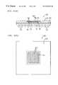
- a semiconductor chip 14is mounted on the upper surface of a substrate 12 using solder “bumps” (balls) 16 , and a thermally conductive structure 18 , which substantially covers one side of substrate 12 (including semiconductor chip 14 ) and is bonded with adhesive agent 20 to the upper surface of the substrate (that on which the chip is located). Furthermore, underfill 22 is deposited between the substrate 12 and the semiconductor chip 14 , and around solder bumps 24 (which are electrically connected to wiring by through holes (not shown)) formed in the substrate and having end portions terminating on the outer surface (e.g., with pads or lands) of substrate 12 .
- solder bumps 24which are electrically connected to wiring by through holes (not shown)
- substrate 12It is preferred to use an organic material for substrate 12 .
- Known dielectric materials having high stiffnesssuch as glass epoxy resin or the like may be used for substrate 12 .
- substrate 12On the upper surface of the substrate 12 , conventional wiring (not shown) that is connected electrically to bumps 16 of the semiconductor chip is formed.
- wiringcomprises a pattern of metal (usually copper) thin lines which couple various pads, lands or the like.
- a flip-chip type semiconductor chipwhich can be mounted horizontally on the substrate 12 through bumps 16 .
- a flip-chipis called this because its contact side is inverted during positioning and faces downward toward the awaiting substrate (e.g., printed circuit board, or PCB) on which it is finally positioned.
- the awaiting substratee.g., printed circuit board, or PCB
- package 10be a BGA module; however, the invention is not limited to only such packages.
- the underfill 22 positioned between substrate 12 and the conductor chip 14 mounted thereonis used to protect the bumps 16 during changes in temperature; therefore, such materials as epoxy materials comprising silica (SiO 2 ) and the like can be used as the material for this underfill.
- Structure 18includes an open (or hollow) portion 26 for accommodating the semiconductor chip 14 and substantially covering it when the structure is in final position on substrate 12 .
- Open portion 26includes space 28 as shown.
- the structure 18is formed by using a material having substantially the same coefficient of thermal expansion (CTE) as substrate 12 .
- CTEcoefficient of thermal expansion
- FR4epoxy resin materials
- aluminum alloy with a relatively low linear expansion coefficientthermal expansion coefficient of 16 ⁇ 10 ⁇ 6 (1/° C.)
- a copper alloythermal expansion coefficient of 15 ⁇ 10 ⁇ 6 (1/° C.
- structure 18should be substantially similar to that of substrate 12 ; however, structure 18 is not to be so limited. Further, metal or metal alloy materials with high stiffness are used for structure 18 .
- the structure 18is located on substrate 12 by covering semiconductor chip 14 ; therefore, it is necessary that heat generated from semiconductor chip 14 be passed to the outside of structure 18 . For this reason, structure 18 is preferably a material with excellent thermal conductivity. If of metal or metal alloy, structure 18 would possess both features (stiffness and heat transfer).
- package 10when structure 18 has the same or about the same thermal expansion coefficient as substrate 12 , even if the semiconductor device 10 is affected by a change in temperature from the outside or by the heat generated from the chip, package 10 is not warped as a whole because substrate 12 thermally expands and contracts in the same manner as structure 18 . Therefore, effective bonding at the solder ball bumps is maintained and the reliability of these bonded packages is dramatically improved.
- the substrate 12 of structure 30is of substantially the same construction as the substrate in FIG. 1 (and preferably of similar material).
- structure 30includes a flat structure 30 a , which is of nearly identical shape as substrate 12 , in combination with spacing member(s) 30 b to assure space for semiconductor chip 14 .
- the flat member 30 a and the spacing member(s) 30 bare bonded to substrate 12 with adhesive 20 .
- the structure 30(of parts 30 a and 30 b ) has the same thermal expansion coefficient as substrate 12 , substantially no warpage will occur in the resulting package 32 .
- the structure which covers the semiconductor chip while mounted on the substrate 12can also be of a composite material comprising a layer 36 of film, sheet, mesh or linear member made of metal or metal alloy, and a synthetic resin layer 38 . If there is no singular material for the structure that has substantially the same CTE as substrate 12 , the structure 34 may be comprised of multiple materials, so that the CTE of these two components are substantially the same.
- structure 34may be comprised of more layers of such materials than those illustrated in FIG. 3 .
- structure 34may also include a single layer for layer 36 , wherein linear members made of metal or alloy are arranged lengthwise and crosswise, this then used in combination with the synthetic resin layer 38 .
- structure 34can even be molded as such after fine powder of metal or alloy is mixed and kneaded with the synthetic resin.
- the synthetic resin used hereinis not particularly limited to only one kind, but a mixture of several kinds of synthetic resins can be also used. In any case, it is preferable that the CTE of structure 34 be the same or about the same as that of the substrate 12 .
- structure 42 of package 40have multiple openings 44 , at least on the area adjacent chip 14 .
- heat generated from semiconductor chip 14will exit through openings 44 to the environment surrounding package 40 .
- structure 42is not necessarily made of metal or alloy with high thermal conductivity, but it may be made of the same dielectric resin material as organic substrate 12 . It is also possible to provide such multiple openings in the structures in FIGS. 1-3.
- structure 46may also include openings 48 at other locations therein, which openings 48 may be filled with synthetic resin 50 .
- openings 48may be filled with synthetic resin 50 .
- Such filled openingsalso possess substantially the same CTE as substrate 12 . In such an embodiment, the same positive effects realized in the above embodiments can be obtained.
- Openings 48 and 44 described aboveare not limited to having a round configuration as shown, but instead can each be of a rectangular, polygonal or oval shape, or various combinations thereof. In addition, these openings can be arranged in a grid, zigzag, or other pattern, thus not being particularly limited to the pattern shown in the drawings.
- structure 58while positioned on the substrate's upper surface, does not necessarily cover the whole of said surface.
- slight warpagemay occur at the bonded location of semiconductor chip 14 (due to the difference in CTEs between the chip and substrate), the uncovered part of the substrate does not warp. This combination assures minimal warpage, if any, at the bonding site which is tolerable for the present invention without causing bump disconnection.
- structure 60may only cover the surroundings of the semiconductor chip on substrate 12 .
- structure 60it is preferable that structure 60 have the same or about the same CTE as substrate 12 , and be resistant to bending.
- members 60 a and 60 c of structure 60expand in the direction of the length members 60 b and 60 d (which are normal to members 60 a and 60 c ) this movement separates one from the others.
- members 60 b and 60 dexpand in the length direction
- members 60 a and 60 calso move in a direction that separates these members from each other. The same positive effects as in the above embodiments can be obtained in this embodiment.
- the semiconductor devicecan be formed by locating the structure 62 (which has the hollow part 26 covering at least the outer surface of the semiconductor chip and has the same or about the same CTE as structure 62 ) on the surface of substrate 12 , filling adhesive material in the space 28 between hollow part 26 of structure 62 and the semiconductor device 14 , and bonding the substrate 12 and the semiconductor chip to the structure.
- Positioning structure 62results in the package getting thicker. For this reason, it is desirable to make structure 62 as thin as possible. However, should structure 62 become too thin, the strength of hollow part 26 also decreases.
- adhesive material 64 in the spaces 28 between hollow part 26the strength of the hollow part can be dramatically increased, allowing for such a package. Further, by filling with adhesive material in this manner, hermeticity and moisture-proofing of the package is assured.
- Package 70 in FIG. 9has a structure 68 as big as its substrate 12 .
- structure 68By making structure 68 this big, the strength of the package is increased. Therefore, a package which prevents warpage can be achieved.
- the resin used for underfill 22can be used as the adhesive agent 64 .
- the structures 62 and 68are symmetrical about the semiconductor chip 14 , to further assure very little, if any, warpage. It is preferable in such an arrangement that an adhesive material with high thermal conductivity be used for adhesive material 64 .
- the heat generated from semiconductor chip 14is mainly directed through structures 62 or 68 before passing externally of the package. For this reason, it is preferable that structures 62 or 68 be made of metal or metal alloy with high thermal conductivity.
- a simple resin or a mixture with resin and metal powdercan be used as the adhesive material 64 for such structures; however, it is preferable to use an adhesive material with higher thermal conductivity.
- a flexible substratewhen such a substrate is bonded to the structure, residual tensile stresses in the substrate do not adversely affect the semiconductor chip and bonded part.
- residual tensile stressBy providing residual tensile stress to the substrate, even when the structure has slightly different thermal expansion coefficient from that of the substrate, no warpage occurs in the package because the residual tension stress absorbs the difference within the range of elongation.
- the package of the present inventionmay be the pin-type packages or similar such packages.
Landscapes
- Engineering & Computer Science (AREA)
- Physics & Mathematics (AREA)
- Condensed Matter Physics & Semiconductors (AREA)
- General Physics & Mathematics (AREA)
- Computer Hardware Design (AREA)
- Microelectronics & Electronic Packaging (AREA)
- Power Engineering (AREA)
- Manufacturing & Machinery (AREA)
- Chemical & Material Sciences (AREA)
- Materials Engineering (AREA)
- Wire Bonding (AREA)
- Cooling Or The Like Of Semiconductors Or Solid State Devices (AREA)
Abstract
Description
Claims (14)
Priority Applications (1)
| Application Number | Priority Date | Filing Date | Title |
|---|---|---|---|
| US09/962,817US6562662B2 (en) | 1998-11-05 | 2001-09-25 | Electronic package with bonded structure and method of making |
Applications Claiming Priority (2)
| Application Number | Priority Date | Filing Date | Title |
|---|---|---|---|
| JP31384898AJP3395164B2 (en) | 1998-11-05 | 1998-11-05 | Semiconductor device |
| JP10-313848 | 1998-11-05 |
Related Child Applications (1)
| Application Number | Title | Priority Date | Filing Date |
|---|---|---|---|
| US09/962,817DivisionUS6562662B2 (en) | 1998-11-05 | 2001-09-25 | Electronic package with bonded structure and method of making |
Publications (1)
| Publication Number | Publication Date |
|---|---|
| US6294831B1true US6294831B1 (en) | 2001-09-25 |
Family
ID=18046246
Family Applications (2)
| Application Number | Title | Priority Date | Filing Date |
|---|---|---|---|
| US09/429,154Expired - LifetimeUS6294831B1 (en) | 1998-11-05 | 1999-10-28 | Electronic package with bonded structure and method of making |
| US09/962,817Expired - LifetimeUS6562662B2 (en) | 1998-11-05 | 2001-09-25 | Electronic package with bonded structure and method of making |
Family Applications After (1)
| Application Number | Title | Priority Date | Filing Date |
|---|---|---|---|
| US09/962,817Expired - LifetimeUS6562662B2 (en) | 1998-11-05 | 2001-09-25 | Electronic package with bonded structure and method of making |
Country Status (3)
| Country | Link |
|---|---|
| US (2) | US6294831B1 (en) |
| JP (1) | JP3395164B2 (en) |
| KR (1) | KR20000035001A (en) |
Cited By (40)
| Publication number | Priority date | Publication date | Assignee | Title |
|---|---|---|---|---|
| US6501171B2 (en)* | 2001-01-30 | 2002-12-31 | International Business Machines Corporation | Flip chip package with improved cap design and process for making thereof |
| US6506626B1 (en)* | 2000-05-12 | 2003-01-14 | Siliconware Precision Industries Co., Ltd. | Semiconductor package structure with heat-dissipation stiffener and method of fabricating the same |
| US6624921B1 (en)* | 2001-03-12 | 2003-09-23 | Amkor Technology, Inc. | Micromirror device package fabrication method |
| US6696748B1 (en) | 2002-08-23 | 2004-02-24 | Micron Technology, Inc. | Stress balanced semiconductor packages, method of fabrication and modified mold segment |
| US20040090756A1 (en)* | 2002-11-07 | 2004-05-13 | Kwun-Yo Ho | Chip packaging structure and manufacturing process thereof |
| US20040150118A1 (en)* | 2003-02-03 | 2004-08-05 | Nec Electronics Corporation | Warp-suppressed semiconductor device |
| US6777819B2 (en)* | 2000-12-20 | 2004-08-17 | Siliconware Precision Industries Co., Ltd. | Semiconductor package with flash-proof device |
| US6784536B1 (en)* | 2000-12-08 | 2004-08-31 | Altera Corporation | Symmetric stack up structure for organic BGA chip carriers |
| US20040183169A1 (en)* | 2001-01-04 | 2004-09-23 | Wen-Wen Chiu | IC chip package |
| US6798053B2 (en)* | 2001-01-04 | 2004-09-28 | Wen-Wen Chiu | IC chip package |
| US6844622B2 (en)* | 2001-06-04 | 2005-01-18 | Siliconware Precision Industries Co., Ltd. | Semiconductor package with heat sink |
| US20050051893A1 (en)* | 2003-09-05 | 2005-03-10 | Taiwan Semiconductor Manufacturing Co. | SBGA design for low-k integrated circuits (IC) |
| US6882041B1 (en) | 2002-02-05 | 2005-04-19 | Altera Corporation | Thermally enhanced metal capped BGA package |
| US6897123B2 (en) | 2001-03-05 | 2005-05-24 | Agityne Corporation | Bonding of parts with dissimilar thermal expansion coefficients |
| US6963126B2 (en)* | 2000-09-06 | 2005-11-08 | Sanyo Electric Co., Ltd. | Semiconductor device with under-fill material below a surface of a semiconductor chip |
| US20060081978A1 (en)* | 2004-10-20 | 2006-04-20 | Siliconware Precision Industries Co., Ltd. | Heat dissipating package structure and method for fabricating the same |
| US7042072B1 (en)* | 2002-08-02 | 2006-05-09 | Amkor Technology, Inc. | Semiconductor package and method of manufacturing the same which reduces warpage |
| US20060278969A1 (en)* | 2005-06-14 | 2006-12-14 | Micron Technology, Inc. | Methods for reducing stress in microelectronic devices and microelectronic devices formed using such methods |
| US20070045796A1 (en)* | 2005-08-19 | 2007-03-01 | Micron Technology, Inc. | Microelectronic devices, stacked microelectronic devices, and methods for manufacturing microelectronic devices |
| US20070108634A1 (en)* | 2003-12-05 | 2007-05-17 | Kazushi Higashi | Packaged electronic element and method of producing electronic element package |
| US20070152323A1 (en)* | 2003-05-30 | 2007-07-05 | Jack Bish | Integrated heat spreader lid |
| US20080224329A1 (en)* | 2007-03-13 | 2008-09-18 | Micron Technology, Inc. | Packaged microelectronic devices and methods for manufacturing packaged microelectronic devices |
| US20090001555A1 (en)* | 2007-06-26 | 2009-01-01 | Nec Electronics Corporation | Semiconductor device having metal cap |
| US20090127689A1 (en)* | 2005-08-26 | 2009-05-21 | Micron Technology, Inc. | Microelectronic device packages, stacked microelectronic device packages, and methods for manufacturing microelectronic devices |
| US20090140402A1 (en)* | 2007-12-03 | 2009-06-04 | Panasonic Corporation | Semiconductor device and method for manufacturing the same |
| US20090244860A1 (en)* | 2008-03-26 | 2009-10-01 | Nec Corporation | Mounting structure of semiconductor device and electronic apparatus using thereof |
| US20090243075A1 (en)* | 2008-03-26 | 2009-10-01 | Nec Corporation | Mounting structure of semiconductor device and electronic apparatus using same |
| US20100079957A1 (en)* | 2008-09-30 | 2010-04-01 | Houle Sabina J | Underfill process and materials for singulated heat spreader stiffener for thin core panel processing |
| US20100096747A1 (en)* | 2008-10-22 | 2010-04-22 | Sony Corporation | Semiconductor device and method of manufacturing the same |
| US20100244236A1 (en)* | 2009-03-26 | 2010-09-30 | Yun Jaeun | Integrated circuit packaging system with heat spreader and method of manufacture thereof |
| US8119924B2 (en) | 2006-03-31 | 2012-02-21 | Nec Corporation | Wiring board, packaging board and electronic device |
| US20120098115A1 (en)* | 2010-10-25 | 2012-04-26 | Elpida Memory, Inc. | Semiconductor device and method of manufacturing the same |
| US20120279060A1 (en)* | 2011-05-06 | 2012-11-08 | National Tsing-Hua University | Methods and apparatuses for non-planar chip assembly |
| US20130243655A1 (en)* | 2011-12-14 | 2013-09-19 | The George Washington University | Flexible IC/microfluidic integration and packaging |
| US8954156B2 (en) | 2010-10-27 | 2015-02-10 | National Tsing Hua University | Methods and apparatuses for configuring artificial retina devices |
| US9114004B2 (en) | 2010-10-27 | 2015-08-25 | Iridium Medical Technology Co, Ltd. | Flexible artificial retina devices |
| US9155881B2 (en) | 2011-05-06 | 2015-10-13 | Iridium Medical Technology Co, Ltd. | Non-planar chip assembly |
| US20190035713A1 (en)* | 2017-07-28 | 2019-01-31 | Qualcomm Incorporated | Systems and methods for cooling an electronic device |
| WO2019091144A1 (en)* | 2017-11-13 | 2019-05-16 | 华为技术有限公司 | Encapsulation structure and electronic apparatus |
| TWI757554B (en)* | 2018-08-24 | 2022-03-11 | 日月光半導體製造股份有限公司 | Semiconductor device package |
Families Citing this family (21)
| Publication number | Priority date | Publication date | Assignee | Title |
|---|---|---|---|---|
| KR100394809B1 (en)* | 2001-08-09 | 2003-08-14 | 삼성전자주식회사 | Semiconductor package and method for manufacturing the same |
| US6787899B2 (en) | 2002-03-12 | 2004-09-07 | Intel Corporation | Electronic assemblies with solidified thixotropic thermal interface material |
| US6657311B1 (en)* | 2002-05-16 | 2003-12-02 | Texas Instruments Incorporated | Heat dissipating flip-chip ball grid array |
| JP2004031651A (en) | 2002-06-26 | 2004-01-29 | Sony Corp | Element mounting substrate and its manufacturing method |
| AU2003286821A1 (en)* | 2002-11-01 | 2004-06-07 | Cooligy, Inc. | Optimal spreader system, device and method for fluid cooled micro-scaled heat exchange |
| US8464781B2 (en)* | 2002-11-01 | 2013-06-18 | Cooligy Inc. | Cooling systems incorporating heat exchangers and thermoelectric layers |
| US20040112571A1 (en)* | 2002-11-01 | 2004-06-17 | Cooligy, Inc. | Method and apparatus for efficient vertical fluid delivery for cooling a heat producing device |
| US20050211418A1 (en)* | 2002-11-01 | 2005-09-29 | Cooligy, Inc. | Method and apparatus for efficient vertical fluid delivery for cooling a heat producing device |
| US7836597B2 (en) | 2002-11-01 | 2010-11-23 | Cooligy Inc. | Method of fabricating high surface to volume ratio structures and their integration in microheat exchangers for liquid cooling system |
| US20040233639A1 (en)* | 2003-01-31 | 2004-11-25 | Cooligy, Inc. | Removeable heat spreader support mechanism and method of manufacturing thereof |
| US7616444B2 (en) | 2004-06-04 | 2009-11-10 | Cooligy Inc. | Gimballed attachment for multiple heat exchangers |
| US7642628B2 (en)* | 2005-01-11 | 2010-01-05 | Rosemount Inc. | MEMS packaging with improved reaction to temperature changes |
| KR100824250B1 (en)* | 2005-08-01 | 2008-04-24 | 엔이씨 일렉트로닉스 가부시키가이샤 | Semiconductor Packages Featuring Metal Lead Members |
| JP2007042719A (en) | 2005-08-01 | 2007-02-15 | Nec Electronics Corp | Semiconductor device |
| WO2007058096A1 (en) | 2005-11-18 | 2007-05-24 | Nec Corporation | Mounted substrate and electronic equipment |
| US7913719B2 (en) | 2006-01-30 | 2011-03-29 | Cooligy Inc. | Tape-wrapped multilayer tubing and methods for making the same |
| US7799542B2 (en)* | 2006-06-29 | 2010-09-21 | The Invention Science Fund I, Llc | Apparatus for arbitrary peptide synthesis |
| US9861234B2 (en)* | 2007-02-15 | 2018-01-09 | Illinois Tool Works, Inc. | Oil reclamation device and process |
| US7964444B2 (en)* | 2007-02-15 | 2011-06-21 | International Business Machines Corporation | Method and apparatus for manufacturing electronic integrated circuit chip |
| JP4933934B2 (en)* | 2007-03-28 | 2012-05-16 | ラピスセミコンダクタ株式会社 | Semiconductor device and manufacturing method of semiconductor device |
| US8313984B2 (en) | 2008-03-19 | 2012-11-20 | Ati Technologies Ulc | Die substrate with reinforcement structure |
Citations (15)
| Publication number | Priority date | Publication date | Assignee | Title |
|---|---|---|---|---|
| JPS62249429A (en) | 1986-04-23 | 1987-10-30 | Hitachi Ltd | semiconductor equipment |
| JPH04291251A (en) | 1990-11-19 | 1992-10-15 | E I Du Pont De Nemours & Co | Mixture phosphor x-line intensifying screen improved image-dissection |
| US5178962A (en)* | 1989-03-20 | 1993-01-12 | Hitachi, Ltd. | Metal-organic macromolecular synthetic resin composite and process for producing the same |
| JPH055300A (en) | 1991-06-28 | 1993-01-14 | Kuraray Co Ltd | Fiberboard manufacturing method |
| JPH05206307A (en) | 1992-01-24 | 1993-08-13 | Toshiba Corp | Semiconductor device |
| US5324888A (en)* | 1992-10-13 | 1994-06-28 | Olin Corporation | Metal electronic package with reduced seal width |
| JPH07297325A (en) | 1994-04-28 | 1995-11-10 | Toshiba Corp | Leadless chip carrier type electronic components |
| US5473512A (en)* | 1993-12-16 | 1995-12-05 | At&T Corp. | Electronic device package having electronic device boonded, at a localized region thereof, to circuit board |
| US5473191A (en)* | 1994-02-16 | 1995-12-05 | Mitsubishi Denki Kabushiki Kaisha | Hybrid integrated circuit device with apertured cover |
| US5734201A (en)* | 1993-11-09 | 1998-03-31 | Motorola, Inc. | Low profile semiconductor device with like-sized chip and mounting substrate |
| US5742007A (en)* | 1996-08-05 | 1998-04-21 | Motorola, Inc. | Electronic device package and method for forming the same |
| US5789810A (en)* | 1995-12-21 | 1998-08-04 | International Business Machines Corporation | Semiconductor cap |
| US5889323A (en)* | 1996-08-19 | 1999-03-30 | Nec Corporation | Semiconductor package and method of manufacturing the same |
| US5909057A (en)* | 1997-09-23 | 1999-06-01 | Lsi Logic Corporation | Integrated heat spreader/stiffener with apertures for semiconductor package |
| JPH11340347A (en) | 1998-05-29 | 1999-12-10 | Kyocera Corp | Package for storing semiconductor elements |
Family Cites Families (4)
| Publication number | Priority date | Publication date | Assignee | Title |
|---|---|---|---|---|
| JPH06268020A (en)* | 1993-03-10 | 1994-09-22 | Sumitomo Electric Ind Ltd | Semiconductor device |
| US5532513A (en)* | 1994-07-08 | 1996-07-02 | Johnson Matthey Electronics, Inc. | Metal-ceramic composite lid |
| JP3400877B2 (en) | 1994-12-14 | 2003-04-28 | 三菱電機株式会社 | Semiconductor device and manufacturing method thereof |
| US5868887A (en)* | 1996-11-08 | 1999-02-09 | W. L. Gore & Associates, Inc. | Method for minimizing warp and die stress in the production of an electronic assembly |
- 1998
- 1998-11-05JPJP31384898Apatent/JP3395164B2/ennot_activeExpired - Fee Related
- 1999
- 1999-10-14KRKR1019990044436Apatent/KR20000035001A/ennot_activeCeased
- 1999-10-28USUS09/429,154patent/US6294831B1/ennot_activeExpired - Lifetime
- 2001
- 2001-09-25USUS09/962,817patent/US6562662B2/ennot_activeExpired - Lifetime
Patent Citations (15)
| Publication number | Priority date | Publication date | Assignee | Title |
|---|---|---|---|---|
| JPS62249429A (en) | 1986-04-23 | 1987-10-30 | Hitachi Ltd | semiconductor equipment |
| US5178962A (en)* | 1989-03-20 | 1993-01-12 | Hitachi, Ltd. | Metal-organic macromolecular synthetic resin composite and process for producing the same |
| JPH04291251A (en) | 1990-11-19 | 1992-10-15 | E I Du Pont De Nemours & Co | Mixture phosphor x-line intensifying screen improved image-dissection |
| JPH055300A (en) | 1991-06-28 | 1993-01-14 | Kuraray Co Ltd | Fiberboard manufacturing method |
| JPH05206307A (en) | 1992-01-24 | 1993-08-13 | Toshiba Corp | Semiconductor device |
| US5324888A (en)* | 1992-10-13 | 1994-06-28 | Olin Corporation | Metal electronic package with reduced seal width |
| US5734201A (en)* | 1993-11-09 | 1998-03-31 | Motorola, Inc. | Low profile semiconductor device with like-sized chip and mounting substrate |
| US5473512A (en)* | 1993-12-16 | 1995-12-05 | At&T Corp. | Electronic device package having electronic device boonded, at a localized region thereof, to circuit board |
| US5473191A (en)* | 1994-02-16 | 1995-12-05 | Mitsubishi Denki Kabushiki Kaisha | Hybrid integrated circuit device with apertured cover |
| JPH07297325A (en) | 1994-04-28 | 1995-11-10 | Toshiba Corp | Leadless chip carrier type electronic components |
| US5789810A (en)* | 1995-12-21 | 1998-08-04 | International Business Machines Corporation | Semiconductor cap |
| US5742007A (en)* | 1996-08-05 | 1998-04-21 | Motorola, Inc. | Electronic device package and method for forming the same |
| US5889323A (en)* | 1996-08-19 | 1999-03-30 | Nec Corporation | Semiconductor package and method of manufacturing the same |
| US5909057A (en)* | 1997-09-23 | 1999-06-01 | Lsi Logic Corporation | Integrated heat spreader/stiffener with apertures for semiconductor package |
| JPH11340347A (en) | 1998-05-29 | 1999-12-10 | Kyocera Corp | Package for storing semiconductor elements |
Non-Patent Citations (3)
| Title |
|---|
| Kotthaus et al., "Study of Isotropically Conductive Bondings Filled with Aggregates of Nano-Sized Ag-Particles", IEEE Trans. on Components, Packaging, and Manu. Tech., pp. 15-20, Mar. 1997.* |
| Schaefer et al. "Conductive Adhesives with Improved Thermomechanical Properties", Proceedings of 3rd International Conf. on Adhesive Joining and Coating Tech. in Elec. Manu., pp. 278-281, Sep. 28-30, 1998.* |
| Wong et al., "Fast-Flow Underfill Encapsulant: Flow Rate and Coefficient of Thermal Expansion", IEEE Trans. on Components, Packaging, and Manu. Tech., pp. 360-364, Oct. 29-30, 1997.* |
Cited By (95)
| Publication number | Priority date | Publication date | Assignee | Title |
|---|---|---|---|---|
| US6506626B1 (en)* | 2000-05-12 | 2003-01-14 | Siliconware Precision Industries Co., Ltd. | Semiconductor package structure with heat-dissipation stiffener and method of fabricating the same |
| US20030102571A1 (en)* | 2000-05-12 | 2003-06-05 | Siliconware Precision Industries Co., Ltd. | Semiconductor package structure with a heat-dissipation stiffener and method of fabricating the same |
| US6963126B2 (en)* | 2000-09-06 | 2005-11-08 | Sanyo Electric Co., Ltd. | Semiconductor device with under-fill material below a surface of a semiconductor chip |
| US6784536B1 (en)* | 2000-12-08 | 2004-08-31 | Altera Corporation | Symmetric stack up structure for organic BGA chip carriers |
| US6777819B2 (en)* | 2000-12-20 | 2004-08-17 | Siliconware Precision Industries Co., Ltd. | Semiconductor package with flash-proof device |
| US6798053B2 (en)* | 2001-01-04 | 2004-09-28 | Wen-Wen Chiu | IC chip package |
| US20040183169A1 (en)* | 2001-01-04 | 2004-09-23 | Wen-Wen Chiu | IC chip package |
| US6967400B2 (en) | 2001-01-04 | 2005-11-22 | Wen-Wen Chiu | IC chip package |
| US6501171B2 (en)* | 2001-01-30 | 2002-12-31 | International Business Machines Corporation | Flip chip package with improved cap design and process for making thereof |
| US6897123B2 (en) | 2001-03-05 | 2005-05-24 | Agityne Corporation | Bonding of parts with dissimilar thermal expansion coefficients |
| US6624921B1 (en)* | 2001-03-12 | 2003-09-23 | Amkor Technology, Inc. | Micromirror device package fabrication method |
| US7074645B2 (en) | 2001-06-04 | 2006-07-11 | Siliconware Precision Industries Co., Ltd. | Fabrication method of semiconductor package with heat sink |
| US6844622B2 (en)* | 2001-06-04 | 2005-01-18 | Siliconware Precision Industries Co., Ltd. | Semiconductor package with heat sink |
| US20050095875A1 (en)* | 2001-06-04 | 2005-05-05 | Chien-Ping Huang | Fabrication method of semiconductor package with heat sink |
| US6882041B1 (en) | 2002-02-05 | 2005-04-19 | Altera Corporation | Thermally enhanced metal capped BGA package |
| US7042072B1 (en)* | 2002-08-02 | 2006-05-09 | Amkor Technology, Inc. | Semiconductor package and method of manufacturing the same which reduces warpage |
| US6855574B2 (en) | 2002-08-23 | 2005-02-15 | Micron Technology, Inc. | Stress balanced semiconductor packages, method of fabrication and modified mold segment |
| US20040038457A1 (en)* | 2002-08-23 | 2004-02-26 | Thurgood Blaine J. | Stress balanced semiconductor packages, method of fabrication and modified mold segment |
| US6696748B1 (en) | 2002-08-23 | 2004-02-24 | Micron Technology, Inc. | Stress balanced semiconductor packages, method of fabrication and modified mold segment |
| US7084489B2 (en) | 2002-08-23 | 2006-08-01 | Micron Technology, Inc. | Computer system including at least one stress balanced semiconductor package |
| US20050018515A1 (en)* | 2002-08-23 | 2005-01-27 | Thurgood Blaine J. | Stress balanced semiconductor packages, method of fabrication and modified mold segment |
| US20040090756A1 (en)* | 2002-11-07 | 2004-05-13 | Kwun-Yo Ho | Chip packaging structure and manufacturing process thereof |
| US6951773B2 (en)* | 2002-11-07 | 2005-10-04 | Via Technologies, Inc. | Chip packaging structure and manufacturing process thereof |
| US8324718B2 (en) | 2003-02-03 | 2012-12-04 | Renesas Electronics Corporation | Warp-suppressed semiconductor device |
| US20040150118A1 (en)* | 2003-02-03 | 2004-08-05 | Nec Electronics Corporation | Warp-suppressed semiconductor device |
| US20100230797A1 (en)* | 2003-02-03 | 2010-09-16 | Hirokazu Honda | Warp-suppressed semiconductor device |
| US7728440B2 (en)* | 2003-02-03 | 2010-06-01 | Nec Electronics Corporation | Warp-suppressed semiconductor device |
| EP1629532A4 (en)* | 2003-05-30 | 2009-02-18 | Honeywell Int Inc | Integrated heat spreader lid |
| US20070152323A1 (en)* | 2003-05-30 | 2007-07-05 | Jack Bish | Integrated heat spreader lid |
| US7518219B2 (en) | 2003-05-30 | 2009-04-14 | Honeywell International Inc. | Integrated heat spreader lid |
| US20050051893A1 (en)* | 2003-09-05 | 2005-03-10 | Taiwan Semiconductor Manufacturing Co. | SBGA design for low-k integrated circuits (IC) |
| US7692292B2 (en) | 2003-12-05 | 2010-04-06 | Panasonic Corporation | Packaged electronic element and method of producing electronic element package |
| US20070108634A1 (en)* | 2003-12-05 | 2007-05-17 | Kazushi Higashi | Packaged electronic element and method of producing electronic element package |
| US20060081978A1 (en)* | 2004-10-20 | 2006-04-20 | Siliconware Precision Industries Co., Ltd. | Heat dissipating package structure and method for fabricating the same |
| US7745262B2 (en) | 2004-10-20 | 2010-06-29 | Siliconware Precision Industries Co., Ltd. | Heat dissipating package structure and method for fabricating the same |
| US20100041181A1 (en)* | 2004-10-20 | 2010-02-18 | Siliconware Precision Industries Co., Ltd. | Heat dissipating package structure and method for fabricating the same |
| US7615862B2 (en)* | 2004-10-20 | 2009-11-10 | Siliconware Precision Industries Co., Ltd. | Heat dissipating package structure and method for fabricating the same |
| US20090275173A1 (en)* | 2005-06-14 | 2009-11-05 | Micron Technology, Inc. | Methods for reducing stress in microelectronic devices and microelectronic devices formed using such methods |
| US20060278969A1 (en)* | 2005-06-14 | 2006-12-14 | Micron Technology, Inc. | Methods for reducing stress in microelectronic devices and microelectronic devices formed using such methods |
| US7573125B2 (en) | 2005-06-14 | 2009-08-11 | Micron Technology, Inc. | Methods for reducing stress in microelectronic devices and microelectronic devices formed using such methods |
| US8084296B2 (en) | 2005-06-14 | 2011-12-27 | Micron Technology, Inc. | Methods for reducing stress in microelectronic devices and microelectronic devices formed using such methods |
| US8823159B2 (en) | 2005-08-19 | 2014-09-02 | Micron Technology, Inc. | Stacked microelectronic devices |
| US9640458B2 (en) | 2005-08-19 | 2017-05-02 | Micron Technology, Inc. | Stacked microelectronic devices |
| US11239128B2 (en) | 2005-08-19 | 2022-02-01 | Micron Technology, Inc. | Microelectronic devices, stacked microelectronic devices, and methods for manufacturing microelectronic devices |
| US20090239337A1 (en)* | 2005-08-19 | 2009-09-24 | Micron Technology, Inc. | Microelectronic devices, stacked microelectronic devices, and methods for manufacturing microelectronic devices |
| US7557443B2 (en) | 2005-08-19 | 2009-07-07 | Micron Technology, Inc. | Microelectronic devices, stacked microelectronic devices, and methods for manufacturing microelectronic devices |
| US8507318B2 (en) | 2005-08-19 | 2013-08-13 | Micron Technology, Inc. | Method for manufacturing microelectronic devices |
| US20070045796A1 (en)* | 2005-08-19 | 2007-03-01 | Micron Technology, Inc. | Microelectronic devices, stacked microelectronic devices, and methods for manufacturing microelectronic devices |
| US10431513B2 (en) | 2005-08-19 | 2019-10-01 | Micron Technology, Inc. | Microelectronic devices, stacked microelectronic devices, and methods for manufacturing microelectronic devices |
| US20090127689A1 (en)* | 2005-08-26 | 2009-05-21 | Micron Technology, Inc. | Microelectronic device packages, stacked microelectronic device packages, and methods for manufacturing microelectronic devices |
| US8519523B2 (en) | 2005-08-26 | 2013-08-27 | Micron Technology, Inc. | Microelectronic device packages, stacked microelectronic device packages, and methods for manufacturing microelectronic devices |
| US10861824B2 (en) | 2005-08-26 | 2020-12-08 | Micron Technology, Inc. | Microelectronic device packages, stacked microelectronic device packages, and methods for manufacturing microelectronic devices |
| US9583476B2 (en) | 2005-08-26 | 2017-02-28 | Micron Technology, Inc. | Microelectronic device packages, stacked microelectronic device packages, and methods for manufacturing microelectronic devices |
| US10153254B2 (en) | 2005-08-26 | 2018-12-11 | Micron Technology, Inc. | Microelectronic device packages, stacked microelectronic device packages, and methods for manufacturing microelectronic devices |
| US9299684B2 (en) | 2005-08-26 | 2016-03-29 | Micron Technology, Inc. | Microelectronic device packages, stacked microelectronic device packages, and methods for manufacturing microelectronic devices |
| US8030748B2 (en) | 2005-08-26 | 2011-10-04 | Micron Technology, Inc. | Microelectronic device packages, stacked microelectronic device packages, and methods for manufacturing microelectronic devices |
| US8119924B2 (en) | 2006-03-31 | 2012-02-21 | Nec Corporation | Wiring board, packaging board and electronic device |
| US20110233740A1 (en)* | 2007-03-13 | 2011-09-29 | Micron Technology, Inc. | Packaged microelectronic devices and methods for manufacturing packaged microelectronic devices |
| US10692827B2 (en) | 2007-03-13 | 2020-06-23 | Micron Technology, Inc. | Packaged microelectronic devices and methods for manufacturing packaged microelectronic devices |
| US20080224329A1 (en)* | 2007-03-13 | 2008-09-18 | Micron Technology, Inc. | Packaged microelectronic devices and methods for manufacturing packaged microelectronic devices |
| US7955898B2 (en) | 2007-03-13 | 2011-06-07 | Micron Technology, Inc. | Packaged microelectronic devices and methods for manufacturing packaged microelectronic devices |
| US9812415B2 (en) | 2007-03-13 | 2017-11-07 | Micron Technology, Inc. | Packaged microelectronic devices and methods for manufacturing packaged microelectronic devices |
| US10163826B2 (en) | 2007-03-13 | 2018-12-25 | Micron Technology, Inc. | Packaged microelectronic devices and methods for manufacturing packaged microelectronic devices |
| US8866272B2 (en) | 2007-03-13 | 2014-10-21 | Micron Technology, Inc. | Packaged microelectronic devices and methods for manufacturing packaged microelectronic devices |
| US8076771B2 (en)* | 2007-06-26 | 2011-12-13 | Renesas Electronics Corporation | Semiconductor device having metal cap divided by slit |
| US20090001555A1 (en)* | 2007-06-26 | 2009-01-01 | Nec Electronics Corporation | Semiconductor device having metal cap |
| US20110001225A1 (en)* | 2007-12-03 | 2011-01-06 | Panasonic Corporation | Semiconductor device and method for manufacturing the same |
| US20090140402A1 (en)* | 2007-12-03 | 2009-06-04 | Panasonic Corporation | Semiconductor device and method for manufacturing the same |
| US7820486B2 (en) | 2007-12-03 | 2010-10-26 | Panasonic Corporation | Method of fabricating a semiconductor device having a heat sink with an exposed surface |
| US20090243075A1 (en)* | 2008-03-26 | 2009-10-01 | Nec Corporation | Mounting structure of semiconductor device and electronic apparatus using same |
| US8093706B2 (en) | 2008-03-26 | 2012-01-10 | Nec Corporation | Mounting structure of semiconductor device and electronic apparatus using same |
| US20090244860A1 (en)* | 2008-03-26 | 2009-10-01 | Nec Corporation | Mounting structure of semiconductor device and electronic apparatus using thereof |
| US8130503B2 (en) | 2008-03-26 | 2012-03-06 | Nec Corporation | Mounting structure of semiconductor device and electronic apparatus using thereof |
| US20100079957A1 (en)* | 2008-09-30 | 2010-04-01 | Houle Sabina J | Underfill process and materials for singulated heat spreader stiffener for thin core panel processing |
| US8390112B2 (en)* | 2008-09-30 | 2013-03-05 | Intel Corporation | Underfill process and materials for singulated heat spreader stiffener for thin core panel processing |
| US20100096747A1 (en)* | 2008-10-22 | 2010-04-22 | Sony Corporation | Semiconductor device and method of manufacturing the same |
| US8334591B2 (en)* | 2008-10-22 | 2012-12-18 | Sony Corporation | Semiconductor device and method of manufacturing the same |
| US20100244236A1 (en)* | 2009-03-26 | 2010-09-30 | Yun Jaeun | Integrated circuit packaging system with heat spreader and method of manufacture thereof |
| US8415204B2 (en) | 2009-03-26 | 2013-04-09 | Stats Chippac Ltd. | Integrated circuit packaging system with heat spreader and method of manufacture thereof |
| US20120098115A1 (en)* | 2010-10-25 | 2012-04-26 | Elpida Memory, Inc. | Semiconductor device and method of manufacturing the same |
| US8872325B2 (en)* | 2010-10-25 | 2014-10-28 | Ps4 Luxco S.A.R.L. | Semiconductor device including an insulating layer and heat sink plates formed in the insulating layer |
| US9114004B2 (en) | 2010-10-27 | 2015-08-25 | Iridium Medical Technology Co, Ltd. | Flexible artificial retina devices |
| US8954156B2 (en) | 2010-10-27 | 2015-02-10 | National Tsing Hua University | Methods and apparatuses for configuring artificial retina devices |
| US9155881B2 (en) | 2011-05-06 | 2015-10-13 | Iridium Medical Technology Co, Ltd. | Non-planar chip assembly |
| US9731130B2 (en) | 2011-05-06 | 2017-08-15 | Iridium Medical Technology Co, Ltd. | Flexible artificial retina device |
| US9224716B2 (en) | 2011-05-06 | 2015-12-29 | Iridium Medical Technology Co., Ltd. | Method for non-planar chip assembly |
| US20120279060A1 (en)* | 2011-05-06 | 2012-11-08 | National Tsing-Hua University | Methods and apparatuses for non-planar chip assembly |
| US8613135B2 (en)* | 2011-05-06 | 2013-12-24 | National Tsing Hua University | Method for non-planar chip assembly |
| US9116145B2 (en)* | 2011-12-14 | 2015-08-25 | The George Washington University | Flexible IC/microfluidic integration and packaging |
| US20130243655A1 (en)* | 2011-12-14 | 2013-09-19 | The George Washington University | Flexible IC/microfluidic integration and packaging |
| US10622282B2 (en)* | 2017-07-28 | 2020-04-14 | Qualcomm Incorporated | Systems and methods for cooling an electronic device |
| US20190035713A1 (en)* | 2017-07-28 | 2019-01-31 | Qualcomm Incorporated | Systems and methods for cooling an electronic device |
| CN109786336A (en)* | 2017-11-13 | 2019-05-21 | 华为技术有限公司 | Encapsulating structure and electronic device |
| WO2019091144A1 (en)* | 2017-11-13 | 2019-05-16 | 华为技术有限公司 | Encapsulation structure and electronic apparatus |
| TWI757554B (en)* | 2018-08-24 | 2022-03-11 | 日月光半導體製造股份有限公司 | Semiconductor device package |
Also Published As
| Publication number | Publication date |
|---|---|
| US6562662B2 (en) | 2003-05-13 |
| KR20000035001A (en) | 2000-06-26 |
| US20020011668A1 (en) | 2002-01-31 |
| JP3395164B2 (en) | 2003-04-07 |
| JP2000150695A (en) | 2000-05-30 |
Similar Documents
| Publication | Publication Date | Title |
|---|---|---|
| US6294831B1 (en) | Electronic package with bonded structure and method of making | |
| JP2570498B2 (en) | Integrated circuit chip carrier | |
| US5535101A (en) | Leadless integrated circuit package | |
| US5859474A (en) | Reflow ball grid array assembly | |
| US5835355A (en) | Tape ball grid array package with perforated metal stiffener | |
| US6756685B2 (en) | Semiconductor device | |
| US6396136B2 (en) | Ball grid package with multiple power/ground planes | |
| KR100294958B1 (en) | Mounting structure for one or more semiconductor devices | |
| US6084308A (en) | Chip-on-chip integrated circuit package and method for making the same | |
| US6734557B2 (en) | Semiconductor device | |
| US5608262A (en) | Packaging multi-chip modules without wire-bond interconnection | |
| US7968799B2 (en) | Interposer, electrical package, and contact structure and fabricating method thereof | |
| KR100702969B1 (en) | Board Mount Structure of BA Type Semiconductor Chip Package with Dummy Solder Ball | |
| US5510956A (en) | Electronic part unit or assembly having a plurality of electronic parts enclosed within a metal enclosure member mounted on a wiring layer | |
| US6816385B1 (en) | Compliant laminate connector | |
| US5956606A (en) | Method for bumping and packaging semiconductor die | |
| US6586830B2 (en) | Semiconductor device with an interposer | |
| US6552267B2 (en) | Microelectronic assembly with stiffening member | |
| US20090045508A1 (en) | Oblong peripheral solder ball pads on a printed circuit board for mounting a ball grid array package | |
| WO2006132151A1 (en) | Interposer and semiconductor device | |
| JPH09129670A (en) | Contact high density type ball grid array package for flip chip | |
| EP0734588A1 (en) | Integrated circuit package | |
| US20070090506A1 (en) | Interposer for compliant interfacial coupling | |
| US6943060B1 (en) | Method for fabricating integrated circuit package with solder bumps | |
| JPH08250835A (en) | Method for mounting lsi package having metallic bump |
Legal Events
| Date | Code | Title | Description |
|---|---|---|---|
| AS | Assignment | Owner name:INTERNATIONAL BUSINESS MACHINES CORPORATION, NEW Y Free format text:ASSIGNMENT OF ASSIGNORS INTEREST;ASSIGNORS:SHISHIDO, ITSUROH;MATSUMOTO, TOSHIHIRO;REEL/FRAME:010353/0384 Effective date:19991019 | |
| STCF | Information on status: patent grant | Free format text:PATENTED CASE | |
| FPAY | Fee payment | Year of fee payment:4 | |
| FPAY | Fee payment | Year of fee payment:8 | |
| FPAY | Fee payment | Year of fee payment:12 | |
| AS | Assignment | Owner name:GLOBALFOUNDRIES U.S. 2 LLC, NEW YORK Free format text:ASSIGNMENT OF ASSIGNORS INTEREST;ASSIGNOR:INTERNATIONAL BUSINESS MACHINES CORPORATION;REEL/FRAME:036550/0001 Effective date:20150629 | |
| AS | Assignment | Owner name:GLOBALFOUNDRIES INC., CAYMAN ISLANDS Free format text:ASSIGNMENT OF ASSIGNORS INTEREST;ASSIGNORS:GLOBALFOUNDRIES U.S. 2 LLC;GLOBALFOUNDRIES U.S. INC.;REEL/FRAME:036779/0001 Effective date:20150910 | |
| AS | Assignment | Owner name:WILMINGTON TRUST, NATIONAL ASSOCIATION, DELAWARE Free format text:SECURITY AGREEMENT;ASSIGNOR:GLOBALFOUNDRIES INC.;REEL/FRAME:049490/0001 Effective date:20181127 | |
| AS | Assignment | Owner name:GLOBALFOUNDRIES INC., CAYMAN ISLANDS Free format text:RELEASE BY SECURED PARTY;ASSIGNOR:WILMINGTON TRUST, NATIONAL ASSOCIATION;REEL/FRAME:054636/0001 Effective date:20201117 | |
| AS | Assignment | Owner name:GLOBALFOUNDRIES U.S. INC., NEW YORK Free format text:RELEASE BY SECURED PARTY;ASSIGNOR:WILMINGTON TRUST, NATIONAL ASSOCIATION;REEL/FRAME:056987/0001 Effective date:20201117 |