US6294813B1 - Information handling system having improved floating gate tunneling devices - Google Patents
Information handling system having improved floating gate tunneling devicesDownload PDFInfo
- Publication number
- US6294813B1 US6294813B1US09/504,496US50449600AUS6294813B1US 6294813 B1US6294813 B1US 6294813B1US 50449600 AUS50449600 AUS 50449600AUS 6294813 B1US6294813 B1US 6294813B1
- Authority
- US
- United States
- Prior art keywords
- interface
- flotox
- information handling
- transistors
- handling system
- Prior art date
- Legal status (The legal status is an assumption and is not a legal conclusion. Google has not performed a legal analysis and makes no representation as to the accuracy of the status listed.)
- Expired - Lifetime
Links
- 230000005641tunnelingEffects0.000titleclaimsabstractdescription34
- 238000003877atomic layer epitaxyMethods0.000claimsabstractdescription14
- 230000015654memoryEffects0.000claimsdescription54
- 239000000758substrateSubstances0.000claimsdescription51
- 210000000746body regionAnatomy0.000claimsdescription18
- 239000012212insulatorSubstances0.000claimsdescription17
- 229910021420polycrystalline siliconInorganic materials0.000claimsdescription15
- 229920005591polysiliconPolymers0.000claimsdescription14
- 238000000034methodMethods0.000abstractdescription37
- 238000003491arrayMethods0.000abstractdescription7
- 238000005516engineering processMethods0.000abstractdescription4
- VYPSYNLAJGMNEJ-UHFFFAOYSA-NSilicium dioxideChemical compoundO=[Si]=OVYPSYNLAJGMNEJ-UHFFFAOYSA-N0.000description36
- 239000004065semiconductorSubstances0.000description19
- 239000000377silicon dioxideSubstances0.000description18
- 238000006243chemical reactionMethods0.000description11
- 229910021419crystalline siliconInorganic materials0.000description8
- 239000002019doping agentSubstances0.000description8
- 239000000463materialSubstances0.000description8
- 235000012431wafersNutrition0.000description8
- 229910018503SF6Inorganic materials0.000description7
- 238000004519manufacturing processMethods0.000description7
- 235000012239silicon dioxideNutrition0.000description6
- 238000004381surface treatmentMethods0.000description6
- WRQGPGZATPOHHX-UHFFFAOYSA-Nethyl 2-oxohexanoateChemical compoundCCCCC(=O)C(=O)OCCWRQGPGZATPOHHX-UHFFFAOYSA-N0.000description5
- XUIMIQQOPSSXEZ-UHFFFAOYSA-NSiliconChemical compound[Si]XUIMIQQOPSSXEZ-UHFFFAOYSA-N0.000description4
- 238000010586diagramMethods0.000description4
- 229910052710siliconInorganic materials0.000description4
- 239000010703siliconSubstances0.000description4
- KRHYYFGTRYWZRS-UHFFFAOYSA-NFluoraneChemical compoundFKRHYYFGTRYWZRS-UHFFFAOYSA-N0.000description3
- 230000005689Fowler Nordheim tunnelingEffects0.000description3
- 229910020175SiOHInorganic materials0.000description3
- 229910045601alloyInorganic materials0.000description3
- 239000000956alloySubstances0.000description3
- 230000004888barrier functionEffects0.000description3
- 238000007796conventional methodMethods0.000description3
- 238000000151depositionMethods0.000description3
- 239000007858starting materialSubstances0.000description3
- 230000015572biosynthetic processEffects0.000description2
- 238000005229chemical vapour depositionMethods0.000description2
- 239000004020conductorSubstances0.000description2
- 230000008021depositionEffects0.000description2
- 230000005684electric fieldEffects0.000description2
- 125000000524functional groupChemical group0.000description2
- 238000004544sputter depositionMethods0.000description2
- SFZCNBIFKDRMGX-UHFFFAOYSA-Nsulfur hexafluorideChemical compoundFS(F)(F)(F)(F)FSFZCNBIFKDRMGX-UHFFFAOYSA-N0.000description2
- 229960000909sulfur hexafluorideDrugs0.000description2
- 230000006978adaptationEffects0.000description1
- 238000007599dischargingMethods0.000description1
- 238000005530etchingMethods0.000description1
- 230000004907fluxEffects0.000description1
- BBKFSSMUWOMYPI-UHFFFAOYSA-Ngold palladiumChemical compound[Pd].[Au]BBKFSSMUWOMYPI-UHFFFAOYSA-N0.000description1
- 238000009499grossingMethods0.000description1
- 239000002784hot electronSubstances0.000description1
- 238000002347injectionMethods0.000description1
- 239000007924injectionSubstances0.000description1
- 229910021421monocrystalline siliconInorganic materials0.000description1
- QPJSUIGXIBEQAC-UHFFFAOYSA-Nn-(2,4-dichloro-5-propan-2-yloxyphenyl)acetamideChemical compoundCC(C)OC1=CC(NC(C)=O)=C(Cl)C=C1ClQPJSUIGXIBEQAC-UHFFFAOYSA-N0.000description1
- 230000003647oxidationEffects0.000description1
- 238000007254oxidation reactionMethods0.000description1
- 239000002245particleSubstances0.000description1
- 238000001020plasma etchingMethods0.000description1
- 239000002243precursorSubstances0.000description1
- 239000000376reactantSubstances0.000description1
- 239000010421standard materialSubstances0.000description1
- 238000003860storageMethods0.000description1
- 238000006467substitution reactionMethods0.000description1
- 238000006557surface reactionMethods0.000description1
Images


Classifications
- H—ELECTRICITY
- H01—ELECTRIC ELEMENTS
- H01L—SEMICONDUCTOR DEVICES NOT COVERED BY CLASS H10
- H01L21/00—Processes or apparatus adapted for the manufacture or treatment of semiconductor or solid state devices or of parts thereof
- H01L21/02—Manufacture or treatment of semiconductor devices or of parts thereof
- H01L21/04—Manufacture or treatment of semiconductor devices or of parts thereof the devices having potential barriers, e.g. a PN junction, depletion layer or carrier concentration layer
- H01L21/18—Manufacture or treatment of semiconductor devices or of parts thereof the devices having potential barriers, e.g. a PN junction, depletion layer or carrier concentration layer the devices having semiconductor bodies comprising elements of Group IV of the Periodic Table or AIIIBV compounds with or without impurities, e.g. doping materials
- H01L21/28—Manufacture of electrodes on semiconductor bodies using processes or apparatus not provided for in groups H01L21/20 - H01L21/268
- H01L21/28008—Making conductor-insulator-semiconductor electrodes
- H01L21/28017—Making conductor-insulator-semiconductor electrodes the insulator being formed after the semiconductor body, the semiconductor being silicon
- H01L21/28158—Making the insulator
- H01L21/28167—Making the insulator on single crystalline silicon, e.g. using a liquid, i.e. chemical oxidation
- H01L21/28194—Making the insulator on single crystalline silicon, e.g. using a liquid, i.e. chemical oxidation by deposition, e.g. evaporation, ALD, CVD, sputtering, laser deposition
- H—ELECTRICITY
- H10—SEMICONDUCTOR DEVICES; ELECTRIC SOLID-STATE DEVICES NOT OTHERWISE PROVIDED FOR
- H10D—INORGANIC ELECTRIC SEMICONDUCTOR DEVICES
- H10D30/00—Field-effect transistors [FET]
- H10D30/60—Insulated-gate field-effect transistors [IGFET]
- H10D30/68—Floating-gate IGFETs
- H10D30/681—Floating-gate IGFETs having only two programming levels
- H10D30/683—Floating-gate IGFETs having only two programming levels programmed by tunnelling of carriers, e.g. Fowler-Nordheim tunnelling
- H—ELECTRICITY
- H10—SEMICONDUCTOR DEVICES; ELECTRIC SOLID-STATE DEVICES NOT OTHERWISE PROVIDED FOR
- H10D—INORGANIC ELECTRIC SEMICONDUCTOR DEVICES
- H10D64/00—Electrodes of devices having potential barriers
- H10D64/01—Manufacture or treatment
- H10D64/031—Manufacture or treatment of data-storage electrodes
- H10D64/035—Manufacture or treatment of data-storage electrodes comprising conductor-insulator-conductor-insulator-semiconductor structures
- H—ELECTRICITY
- H10—SEMICONDUCTOR DEVICES; ELECTRIC SOLID-STATE DEVICES NOT OTHERWISE PROVIDED FOR
- H10D—INORGANIC ELECTRIC SEMICONDUCTOR DEVICES
- H10D64/00—Electrodes of devices having potential barriers
- H10D64/60—Electrodes characterised by their materials
- H10D64/66—Electrodes having a conductor capacitively coupled to a semiconductor by an insulator, e.g. MIS electrodes
- H10D64/68—Electrodes having a conductor capacitively coupled to a semiconductor by an insulator, e.g. MIS electrodes characterised by the insulator, e.g. by the gate insulator
- Y—GENERAL TAGGING OF NEW TECHNOLOGICAL DEVELOPMENTS; GENERAL TAGGING OF CROSS-SECTIONAL TECHNOLOGIES SPANNING OVER SEVERAL SECTIONS OF THE IPC; TECHNICAL SUBJECTS COVERED BY FORMER USPC CROSS-REFERENCE ART COLLECTIONS [XRACs] AND DIGESTS
- Y10—TECHNICAL SUBJECTS COVERED BY FORMER USPC
- Y10S—TECHNICAL SUBJECTS COVERED BY FORMER USPC CROSS-REFERENCE ART COLLECTIONS [XRACs] AND DIGESTS
- Y10S438/00—Semiconductor device manufacturing: process
- Y10S438/964—Roughened surface
Definitions
- the present inventionrelates generally to semiconductor integrated circuits. More particularly, it pertains to an alternate method and structure for improved floating gate tunneling devices.
- Non volatile floating gate tunneling oxide (FLOTOX) devicese.g. FLOTOX transistors
- FLOTOX transistorsFlash memories are one form of FLOTOX devices and electronically erasable and programmable read only memories (EEPROMs) are another. Due to their high density nature, memories formed with FLOTOX transistors have the potential of replacing hard storage disk drives in computer systems. The advantages to this substitution would be in replacing a complex and delicate mechanical system with a rugged and easily portable small solid-state non-volatile memory system. There is also the possibility that given more speed of operation, particularly in the erase operation, that FLOTOX transistors might be used to replace dynamic random access memories (DRAMs). Thus, FLOTOX transistors might eventually have the ability to fill all memory needs in future computer systems.
- DRAMsdynamic random access memories
- FLOTOX transistorscan be electronically programmed, erased, and reprogrammed.
- FLOTOX transistorsa floating gate is electrically isolated and any charge stored on the floating gate is trapped. Storing sufficient charge on the floating gate will create an inversion channel between source and drain of the transistor. Thus, the presence or absence of charge on the floating gate represents two distinct data states.
- FLOTOX transistorsare selectively programmed, or “written to,” by hot electron injection which places a charge on a floating gate during a write.
- the FLOTOX transistorsare selectively erased by Fowler-Nordheim tunneling which removes the a charge from the floating gate.
- a high programming voltageis placed on a control gate. This forces an inversion region to form in the p-type substrate.
- the drain voltageis increased to approximately half the control gate voltage while the source is grounded, increasing the voltage drop between the drain and source. In the presence of the inversion region, the current between the drain and source increases.
- the resulting high electron flow from source to drainincreases the kinetic energy of the electrons. This causes the electrons to gain enough energy to overcome the outside barrier and collect on the floating gate.
- V Ttransistor's threshold voltage
- Sense amplifiersdetect and amplify the transistor current, and output a 0 for a written transistor.
- the floating gatecan be unprogrammed, or “erased,” by grounding the control gate and raising the source voltage to a sufficiently high positive voltage to transfer electrons out of the floating gate to the source terminal of the transistor by tunneling through the insulating gate oxide. After the erase is completed, the lack of charge on the floating gate lowers the cell's V T below the wordline logic 1 voltage. Thus when an erased cell's wordline is brought to a logic 1 during a read, the transistor will turn on and conduct more current than a written cell.
- Some flash devicesuse Fowler-Nordheim tunneling for write as well as erase.
- Fowler-Nordheim tunnelingrequires high voltages, is relatively slow, and introduces erratic over erase and other reliability problems due to the very high erase voltages used.
- These very high erase voltagesare a fundamental problem arising from the high electron affinity of bulk silicon or large grain polysilicon particles used as the floating gate.
- the high electron affinitycreates a very high tunneling barrier and, even with high negative voltages applied to the gate, a large tunneling distance.
- the high tunneling barrier and large tunneling distanceequate to a very low tunneling probability for electrons attempting to leave the floating gate. This results in long write times since the net flux of electrons leaving the floating gate is low or the tunneling current discharging from the floating gate is low.
- a method and structureare provided which create an improved textured surface and improved insulating gate oxide in order to increase low voltage tunneling currents in FLOTOX transistors.
- an illustrative embodiment of the present inventionincludes a non volatile memory cell structure.
- the non volatile memory cell structureincludes a substrate with a textured surface.
- the textured surfaceincludes an array of microtips with each microtip having a top surface.
- the microtips in the arrayhave an average density of 10 12 /cm 2 .
- a tunnel oxide layeris adjacent to the textured substrate.
- the tunnel oxide layeris deposited using binary reaction sequence chemistry.
- a first gateis formed on the tunnel oxide layer.
- An insulator layerformed on the first gate.
- the structurefurther includes a second gate formed on the insulator layer.
- a non volatile memory cell structurein another embodiment, includes a first interface which has spaced source and drain regions and a body region located between the source and drain on a first portion of the interface.
- the first interfacehas a silicon (Si) layer adjacent to a silicon dioxide (SiO 2 ) layer.
- the silicon dioxide (SiO 2 ) layerhas a thickness between 15 and 100 Angstroms ( ⁇ ).
- the silicon dioxide (SiO 2 ) layeris deposited using binary reaction sequence chemistry.
- a second interfaceis adjacent to the first interface.
- a third interfaceis adjacent to the second interface.
- a fourth interfaceis adjacent to the third interface.
- a memory array of non volatile memory cell structuresincludes a number of floating gate tunneling oxide (FLOTOX) transistors.
- FLOTOXfloating gate tunneling oxide
- Each FLOTOX transistorfurther includes a substrate that has a first source/drain region, a second source/drain region, and a body region.
- the substratehas a textured surface which comprises an array of microtips.
- Each microtiphas a top surface.
- the microtips in the array of microtipshave an average density of 10 12 /cm 2 .
- a tunnel oxide layeris formed on the substrate.
- the tunnel oxide layeris deposited using atomic layer epitaxy (ALE).
- a first conductive layeris formed on the tunnel dielectric.
- An insulator layeris formed on the first conductive layer.
- the memory arrayfurther includes a number of wordlines. Each wordline couples the second conductive layer for a number of FLOTOX transistors. A number of bitlines are included such that each bitline couples the second source/drain region for a number of FLOTOX transistors. A number of sense amplifiers are included. The number of sense amplifiers couple to a select number of the number of bitlines. Also, a number of sourcelines are provided. Each sourceline couples a first source/drain region for a number of FLOTOX transistors.
- the information handling systemincludes a memory array and a central processing unit (CPU) coupled together by a system bus.
- the memory arrayincludes the memory array of non volatile memory cell structures described above.
- a method for fabricating a non volatile memory cell structureincludes forming a textured surface on a substrate. Forming the textured surface includes forming an array of microtips so that each microtip has a top surface. Forming the array of microtips includes forming the microtips in the array of microtips to have an average density of 10 12 /cm 2 .
- a tunnel oxide layeris formed on the textured surface. Forming the tunnel oxide layer comprises depositing the tunnel oxide layer on the substrate by using atomic layer epitaxy (ALE). A first gate is formed on the tunnel oxide layer. An insulator layer is formed on the first gate. The method further includes forming a second gate on the insulator layer.
- a method for fabricating a non volatile memory cell structureincludes forming a first interface which has spaced source and drain regions and a body region located between the source and drain regions on a first portion of the first interface.
- a self-structured maskis formed on the first portion of the first interface.
- the first portion of the first interfaceis etched to form a micro-roughened surface.
- the self-structured maskis removed.
- a tunnel oxide layeris deposited on the first portion of the first interface using atomic layer epitaxy (ALE).
- ALEatomic layer epitaxy
- the methodfurther includes forming a second interface adjacent to the first interface.
- a third interfaceis formed adjacent to the second interface.
- a fourth interfaceis formed adjacent to the third interface.
- an improved structure and method for textured surfaces and insulating gate oxides in floating gate tunneling oxide (FLOTOX) devicesare provided.
- the present inventioncapitalizes on using “self-structured masks” and a controlled etch to form nanometer scale microtip arrays in the textured surfaces.
- the microtips in the array of microtipshave a more uniform size and shape and higher density ( ⁇ 10 12 /cm 2 ) at the substrate/tunnel oxide (Si/SiO 2 ) interface than employed in the present FLOTOX technology. This higher density is four orders of magnitude greater than that which had been previously achieved.
- the new method and structureavoid smoothing the microtips arrays during the formation of the insulating gate oxide.
- the new method and structureproduce significantly larger tunneling currents for a given voltage than attained in prior FLOTOX transistors.
- the new method and structureare advantageously suited for the much higher density, non volatile FLOTOX transistors used in flash memories and in electronically eraseable and programmable read only memories (EEPROMs). These FLOTOX transistors are candidates for replacing the low power operation transistors found in DRAMs.
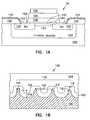
- FIG. 1Ais a cross-sectional view illustrating a non volatile floating gate tunneling oxide (FLOTOX) transistor according to the teachings of the present invention.
- FLOTOXnon volatile floating gate tunneling oxide
- FIG. 1Bis a cross-sectional view illustrating in greater detail an embodiment of an interface region for the FLOTOX transistor shown in FIG. 1 A.
- FIG. 2is a block diagram illustrating an embodiment of a memory array according to the teachings of the present invention.
- FIG. 3is a block diagram illustrating an information handling system according to an embodiment of the present invention.
- FIGS. 4A-4Dillustrate an embodiment of a process of fabrication for a non volatile floating gate tunneling oxide (FLOTOX) transistor according to the teachings of the present invention.
- FLOTOXnon volatile floating gate tunneling oxide
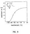
- FIG. 5is a graph illustrating the temperature dependence of anisotropy in a reactive ion etch (RIE) using a sulfur hexafluoride (SF 6 ) gas.
- RIEreactive ion etch
- SF 6sulfur hexafluoride
- wafer and substrate used in the following descriptioninclude any structure having an exposed surface with which to form the integrated circuit (IC) structure of the invention.
- substrateis understood to include semiconductor wafers.
- substrateis also used to refer to semiconductor structures during processing, and may include other layers that have been fabricated thereupon. Both wafer and substrate include doped and undoped semiconductors, epitaxial semiconductor layers supported by a base semiconductor or insulator, as well as other semiconductor structures well known to one skilled in the art.
- conductoris understood to include semiconductors
- insulatoris defined to include any material that is less electrically conductive than the materials referred to as conductors.
- horizontalas used in this application is defined as a plane parallel to the conventional plane or surface of a wafer or substrate, regardless of the orientation of the wafer or substrate.
- verticalrefers to a direction perpendicular to the horizonal as defined above. Prepositions, such as “on”, “upper,” “side” (as in “sidewall”), “higher,” “lower,” “over” and “under” are defined with respect to the conventional plane or surface being on the top surface of the wafer or substrate, regardless of the orientation of the wafer or substrate.
- n+refers to semiconductor material that is heavily doped n-type semiconductor material, e.g., monocrystalline silicon or polycrystalline silicon.
- p+refers to semiconductor material that is heavily doped p-type semiconductor material.
- n ⁇ and p ⁇refer to lightly doped n and p-type semiconductor materials, respectively.
- FIG. 1Ais a cross-sectional view illustrating a non volatile floating gate tunneling oxide (FLOTOX) transistor 50 according to the teachings of the present invention.
- the FLOTOX transistor 50is a non volatile memory cell structure which has a floating gate 104 that can be electrically programmed, erased, and reprogrammed. Flash memory is one form of non volatile memory which implements floating gates. Electronically erasable and programmable read only memories (EEPROMs) are another form. Both types are recognized by those of ordinary skill in the art.
- FIG. 1Aillustrates that FLOTOX transistor 50 includes a body region 101 as part of a substrate 100 .
- Substrate 100includes bulk semiconductor starting material, semiconductor-on-insulator (SOI) starting material, or SOI material that is formed from a bulk semiconductor starting material during processing.
- the body region 101is single crystalline silicon (Si) which has been doped with a p-type dopant to form an p-type body region.
- the body region 101is single crystalline silicon (Si) which has been doped with an n-type dopant to form an n-type body region.
- the FLOTOX transistor 50includes a first source/drain region 120 and a second source/drain region 122 which are formed in the body region 101 portion of the substrate 100 .
- the first and second source/drain regions, 120 and 122are formed of single crystalline silicon (Si) that has been doped with an n-type dopant to form n+ first and second source/drain regions, 120 and 122 .
- the first and second source/drain regions, 120 and 122are formed of single crystalline silicon (Si) which has been doped with p-type dopant to form a p+first and second source/drain regions, 120 and 122 .
- a channel region 124is located in the body region 101 of the substrate 100 between the first and second source/drain regions, 120 and 122 .
- the FLOTOX transistor 50includes electrical contacts 103 which couple to the first and second source/drain regions, 120 and 122 .
- Field oxide regions 105define the boundary of the FLOTOX transistor 50 and serve to electrically isolate the FLOTOX transistor 50 from neighboring devices.
- the FLOTOX transistorfurther includes a tunnel oxide layer 102 located on the substrate surface 150 .
- the tunnel oxide layer 102constitutes a first dielectric layer.
- the tunnel oxide layeris silicon dioxide (SiO 2 ) and covers the channel region 124 as well as portions of the first and second source/drain regions, 120 and 122 respectively.
- the location of the tunnel oxide layer 102 on the substrate surface 150constitutes a first interface.
- a first gate 104is located on the tunnel oxide layer 102 .
- the first gate 104is a first conductive layer and serves as the floating gate 104 .
- the first gate 104is a polysilicon layer.
- the first gate 104forms a second interface in combination with the tunnel oxide layer 102 .
- An insulator layer 106is positioned on top of the first gate 104 .
- the insulator layer 106constitutes a second dielectric layer.
- the insulator layer 106is a silicon dioxide (SiO 2 ) layer.
- the insulator layer 106forms a third interface in combination with the first gate 104 .
- a second gate 108is further included in the FLOTOX transistor.
- the second gate 108is a second conductive layer 108 , which serves as a control gate 108 .
- the second gate 108is located on the insulator layer 106 .
- the union between the second gate 108 and the insulator layer 106forms a fourth interface.
- the second gate 108is a polysilicon layer.
- FIG. 1Bis a cross-sectional view illustrating in greater detail an embodiment of an interface region 130 for the FLOTOX transistor shown in FIG. 1 A.
- the interface region 130 depicted in FIG. 1Bprovides a sample representation of any region between the layered structure of the first gate 104 , the tunnel oxide layer 102 and the substrate surface 150 .
- FIG. 1Billustrates that the substrate surface 150 is textured.
- the substrate surface 150includes an array of microtips 110 .
- the array of microtips 110consists of a multitude of asperities to the substrate surface 150 .
- Each microtiphas a top surface 112 .
- the microtips in array of microtips 110have an average density of approximately 10 12 microtips per square centimeter (10 12 /cm 2 ) of substrate 100 .
- the microtipshave an average height 114 of approximately 7 nanometers (nm).
- the top surfaces 112 of the microtipshave an average diameter 116 of approximately 0.5 nm, and a center to center spacing 118 of the microtips which averages approximately 20 nm.
- FIG. 1 B's illustration of the interface region 130further illustrates the tunnel oxide layer 102 covering the array of microtips 110 .
- the tunnel oxide layer 102 on the array of microtips 110provides a first interface.
- FIG. 1Bfurther illustrates the first gate 104 located on the tunnel oxide layer 102 .
- the junction between the first gate 104 and the tunnel oxide layer 102provides a second interface.
- FIG. 2is a block diagram illustrating an embodiment of a memory array 201 according to the teachings of the present invention.
- the memory array 201is comprised of an array of non volatile memory cell structures 230 which includes a number of individual FLOTOX transistors 200 .
- Each FLOTOX transistor 200includes the non volatile memory cell structure described above in conjunction with FIGS. 1A and 1B.
- the memory array 230includes a number of wordlines, a number of bitlines, and a number of sourcelines. In one embodiment, there are N rows wordlines WL 0 , WL 1 . . . WL N ⁇ 1 , WL N .
- Each of the N rows of wordlinescouples the second conductive layer, or control gate, for a number of FLOTOX transistors 200 in the row.
- array 230has M columns of bitlines BL 0 , BL 1 . . . BL M ⁇ 1 , BL M .
- Each of the M columns of bitlinescouples the second source/drain region for a number of FLOTOX transistor 200 in the column.
- This embodimentfurther includes X columns of sourcelines SL 0 , SL 1 . . . SL X ⁇ 1 , SL X .
- Each of the X sourcelinescouples the first source/drain region for a number of FLOTOX transistors 200 in the column. It should be noted the numbers represented by the variable X, M, and N may be the same or different.
- the N rows wordlines WL 0 , WL 1 . . . WL N ⁇ 1, WL Nare coupled to wordline drivers 210 and communicate with the control gates to selectively read, program, erase, or reprogram the FLOTOX transistors 200 .
- the M columns of bitlinesare coupled to a number of sense amplifiers 203 and serve to transport bits of data information to and from the number of FLOTOX transistors 200 of the memory array 201 .
- a number of bitline drivers 205are coupled to the number of sense amplifiers 203 .
- SL X ⁇ 1 , SL Xare used to couple a power supply 220 (V DD ) to the number of FLOTOX transistors 200 in the memory array 201 .
- V DDpower supply 220
- the read, program and unprogram operations for a non volatile memory cell, of which flash memory is one form and EEPROMS are another,are well known by those of ordinary skill in the art. The actual steps in such processes do not form part of the present invention and thus are not recited in detail here.
- FIG. 3is a block diagram illustrating an information handling system 300 according to an embodiment of the present invention.
- FIG. 3illustrates that information handling system includes a memory 330 .
- the memoryincludes the memory array provided and described above in connection with FIG. 2 .
- the information handling system 300further includes a central processing unit (CPU) 304 .
- the CPUcouples to the memory 330 via a system bus 310 .
- CPUs 304 and system buses 310are well known to those of ordinary skill in the art. These CPUs 304 and system buses 310 are commercially available in many suitable forms for implementation with the present invention. Those skilled in the art will recognize and be able to employ such suitable devices with the present invention. As such, a detailed of these CPUs 304 and system buses 310 is not provided here.
- FIGS. 4A-4Dillustrate an embodiment of a process of fabrication for a non volatile floating gate tunneling oxide (FLOTOX) transistor according to the teachings of the present invention.
- the standard FLOTOX transistorincludes a source, a drain, and a body region all formed within a substrate. The body region separates the source and drain regions. These regions are covered by a tunnel dielectric.
- a floating gateis located on the tunnel dielectric. Further, a control gate is located on the floating gate. A second dielectric layer is interposed between and separates the control gate and the floating gate.
- Standard FLOTOX transistor formation, of this sort,is generally known by those of ordinary skill in the art. Therefore, for succinctness, FIGS.
- 4A-4Dillustrate only the manner in which the substrate surface underneath, and then the tunnel oxide layer thereupon are structured without specific details as to how this region is mask defined or how other portions of the wafer are protected using standard materials and methods.
- the descriptionrelates to the substrate surface and the tunnel oxide layer structure in the body region as well as for portions of the first and second source/drain regions of the FLOTOX transistor.
- FIG. 4Aillustrates the structure after the following series of processing steps.
- the substrate surface 450is cleaned using a wet etch of hydrofluoric acid (HF).
- the substrate 400is single crystalline silicon (Si) which has been doped with p-type dopant to form an p-type body region.
- the substrate 400is single crystalline silicon (Si) which has been doped with a n-type dopant to form a n-type body region.
- the substrate 400is single crystalline silicon (Si) which has been doped with an n-type dopant to form an n+ source/drain region.
- the substrate 400is single crystalline silicon (Si) which has been doped with p-type dopant to form an p+ source/drain region.
- a surface treatment 401is applied to the surface 450 of the substrate 400 .
- the surface treatment 401is a gold-palladium (AuPd) alloy which consist of a 6:4 combination ratio respectively.
- AuPdgold-palladium
- other suitable surface treatments 401can be used.
- the AuPd surface treatment 401is applied to the surface 450 of the substrate 400 by any suitable process such as, for example, by sputtering.
- the AuPd alloyis sputtered onto the surface using conventional techniques known by those of ordinary skill in the field of semiconductor fabrication.
- the AuPd alloyis sputtered on the substrate surface 450 to a thickness of approximately 0.4 nanometers (run).
- the sputtering processresults in a surface treatment 401 of AuPd islands with diameters of approximately 2 nm on 20 nm centers creating a self structured mask.
- FIG. 4Billustrates the structure following the next series of processing steps.
- the substrate 400is dry etched using reactive ion etching (RIE).
- RIEreactive ion etching
- the dry etchis performed using a sulfur hexafluoride (SF 6 ) gas.
- SF 6sulfur hexafluoride
- other compatible etching techniquescan be utilized.
- the dry etchis performed in an rf cathode-coupled, parallel plate plasma etcher with temperature controlling electrodes which regulate the temperature of the substrate 400 .
- Such systemscan maintain the substrate 400 temperature range from ⁇ 150 to +200 degrees Celsius (C). In one exemplary embodiment, the substrate temperature is maintained at ⁇ 80 degrees Celsius.
- the rf power density in the RIE processis 0.2 Watts per cubic centimeter (W/cm 3 ) and the SF 6 gas pressure is kept at 8.6 Pascals (Pa). This process yields an etch rate of 400 nanometers per minute (nm/min).
- the substrateis etched for 1 second.
- the etch under these conditionsproduces an array of microtips 410 .
- the microtips in the array of microtips 410have an average height of 7 nm, a top surface diameter of 0.5 nm with a density of 10 12 microtips per square centimeter (10 12 /cm 2 ).
- the power density and/or SF 6 gas pressurecan be reduced to allow for longer etch times.
- FIG. 5shows the anisotropic temperature dependence of SF 6 in a RIE under the conditions of the exemplary embodiment described above.
- FIG. 4Cillustrates the structure after the next sequence of processing steps.
- the surface treatment 401is removed using any suitable, conventional stripping technique. Such stripping techniques are well know by those practiced in the art of semiconductor fabrication.
- an oxide layer 402is formed across the array of microtips 410 .
- the oxide layer 402forms a first interface in combination with the array of microtips 410 .
- the array of microtipsconstitutes a first portion of the first interface.
- the oxide layer 402is a SiO 2 layer 402 formed using atomic layer epitaxy (ALE). According to this method, atomic layer growth of Silicon dioxide (SiO 2 ) films is achieved by using binary reaction sequence chemistry. In one exemplary embodiment, a binary reaction sequence for the deposition of SiO 2 is:
- each half-reactioninvolves the reaction between a gas phase precursor and a surface functional group, e.g. SiOH* or SiCl*. Surface reaction continues until the initial surface functional groups are replaced by new ones. Once a half-reaction has reached completion, additional reactant exposure should produce no additional growth. In one embodiment the reaction is conducted in a temperature of ⁇ 600 degrees Kelvin (K). Under these conditions, a growth rate for the SiO 2 layer 402 is observed to be 1.1 ⁇ per AB cycle. In one embodiment, the oxide layer 402 is deposited to a thickness between 15 and 100 ⁇ .
- Kdegrees Kelvin
- the oxide layer 402serves as the tunnel oxide layer 402 for the FLOTOX transistor.
- the tunnel oxide layer 402is deposited to the appropriate thickness for the type of FLOTOX transistor desired.
- the oxide layer 402will typically have a thickness of less than 150 Angstroms ( ⁇ ).
- the FLOTOXis of the electronically erasable and programmable read only memory (EEPROM) type the oxide layer 402 will typically have a thickness of 150 ⁇ or greater.
- EEPROMelectronically erasable and programmable read only memory
- FIG. 4Dillustrates the structure following the next sequence of processing steps.
- a first conductive layer 404is formed on the oxide layer 402 .
- the first conductive layer 404is a first gate and serves as the floating gate in a FLOTOX transistor.
- the first conductive layeris formed using any suitable method such as, for example, chemical vapor deposition (CVD).
- CVDchemical vapor deposition
- the first conductive layer 404is polysilicon and forms a second interface in conjunction with the oxide layer 402 .
- the structureis now as appears in FIG. 4 D.
- a second dielectric layeris formed on the floating gate and a second conductive layer, e.g., control gate, is formed on the second dielectric layer according to such conventional methods.
- the second dielectric layer and the control gateform a third and fourth interface, respectively, in the FLOTOX transistor.
- Contact holes and wiring for wordlines, bitlines, and sourcelinesare achieved through conventional processing steps.
- a method and structure for textured surfaces and an improved floating gate oxide layer in floating gate tunneling oxide (FLOTOX) transistorsare provided.
- the present inventioncapitalizes on using “self-structured masks” and a controlled etch to form nanometer scale microtip arrays in the textured surfaces.
- the present inventionalso employs atomic layer epitaxy (ALE) to create an a very conformal tunnel oxide layer which complements the nanometer scale microtip arrays.
- ALEatomic layer epitaxy
- the resulting structureprovides a higher tunneling current than currently exists in FLOTOX technology.
- the improved tunneling currents at low voltagescan make these FLOTOX devices suitable for replacing DRAMS.
Landscapes
- Engineering & Computer Science (AREA)
- Condensed Matter Physics & Semiconductors (AREA)
- Crystallography & Structural Chemistry (AREA)
- General Chemical & Material Sciences (AREA)
- Physics & Mathematics (AREA)
- Chemical Kinetics & Catalysis (AREA)
- Chemical & Material Sciences (AREA)
- General Physics & Mathematics (AREA)
- Manufacturing & Machinery (AREA)
- Computer Hardware Design (AREA)
- Microelectronics & Electronic Packaging (AREA)
- Power Engineering (AREA)
- Non-Volatile Memory (AREA)
- Semiconductor Memories (AREA)
Abstract
Description
Claims (17)
Priority Applications (1)
| Application Number | Priority Date | Filing Date | Title |
|---|---|---|---|
| US09/504,496US6294813B1 (en) | 1998-05-29 | 2000-02-15 | Information handling system having improved floating gate tunneling devices |
Applications Claiming Priority (2)
| Application Number | Priority Date | Filing Date | Title |
|---|---|---|---|
| US09/087,473US6025627A (en) | 1998-05-29 | 1998-05-29 | Alternate method and structure for improved floating gate tunneling devices |
| US09/504,496US6294813B1 (en) | 1998-05-29 | 2000-02-15 | Information handling system having improved floating gate tunneling devices |
Related Parent Applications (1)
| Application Number | Title | Priority Date | Filing Date |
|---|---|---|---|
| US09/087,473DivisionUS6025627A (en) | 1998-05-29 | 1998-05-29 | Alternate method and structure for improved floating gate tunneling devices |
Publications (1)
| Publication Number | Publication Date |
|---|---|
| US6294813B1true US6294813B1 (en) | 2001-09-25 |
Family
ID=22205396
Family Applications (3)
| Application Number | Title | Priority Date | Filing Date |
|---|---|---|---|
| US09/087,473Expired - LifetimeUS6025627A (en) | 1998-05-29 | 1998-05-29 | Alternate method and structure for improved floating gate tunneling devices |
| US09/504,496Expired - LifetimeUS6294813B1 (en) | 1998-05-29 | 2000-02-15 | Information handling system having improved floating gate tunneling devices |
| US09/504,405Expired - Fee RelatedUS6331465B1 (en) | 1998-05-29 | 2000-02-15 | Alternate method and structure for improved floating gate tunneling devices using textured surface |
Family Applications Before (1)
| Application Number | Title | Priority Date | Filing Date |
|---|---|---|---|
| US09/087,473Expired - LifetimeUS6025627A (en) | 1998-05-29 | 1998-05-29 | Alternate method and structure for improved floating gate tunneling devices |
Family Applications After (1)
| Application Number | Title | Priority Date | Filing Date |
|---|---|---|---|
| US09/504,405Expired - Fee RelatedUS6331465B1 (en) | 1998-05-29 | 2000-02-15 | Alternate method and structure for improved floating gate tunneling devices using textured surface |
Country Status (1)
| Country | Link |
|---|---|
| US (3) | US6025627A (en) |
Cited By (40)
| Publication number | Priority date | Publication date | Assignee | Title |
|---|---|---|---|---|
| US6476441B2 (en)* | 1998-05-29 | 2002-11-05 | Micron Technology, Inc. | Method and structure for textured surfaces in floating gate tunneling oxide devices |
| US20030045060A1 (en)* | 2001-08-30 | 2003-03-06 | Micron Technology, Inc. | Crystalline or amorphous medium-k gate oxides, Y2O3 and Gd2O3 |
| US20030057510A1 (en)* | 2001-09-27 | 2003-03-27 | Motoharu Ishii | Capacitance element and boosting circuit using the same |
| US6586797B2 (en) | 2001-08-30 | 2003-07-01 | Micron Technology, Inc. | Graded composition gate insulators to reduce tunneling barriers in flash memory devices |
| US20030235081A1 (en)* | 2002-06-21 | 2003-12-25 | Micron Technology, Inc. | Nanocrystal write once read only memory for archival storage |
| US20030235077A1 (en)* | 2002-06-21 | 2003-12-25 | Micron Technology, Inc. | Write once read only memory employing floating gates |
| US20030235079A1 (en)* | 2002-06-21 | 2003-12-25 | Micron Technology, Inc. | Nor flash memory cell with high storage density |
| US20030235085A1 (en)* | 2002-06-21 | 2003-12-25 | Micron Technology, Inc. | Write once read only memory employing charge trapping in insulators |
| US20030235066A1 (en)* | 2002-06-21 | 2003-12-25 | Micron Technology, Inc. | Ferroelectric write once read only memory for archival storage |
| US20030234420A1 (en)* | 2002-06-21 | 2003-12-25 | Micron Technology, Inc. | Write once read only memory with large work function floating gates |
| US20040004247A1 (en)* | 2002-07-08 | 2004-01-08 | Micron Technology, Inc. | Memory utilizing oxide-nitride nanolaminates |
| US20040004245A1 (en)* | 2002-07-08 | 2004-01-08 | Micron Technology, Inc. | Memory utilizing oxide-conductor nanolaminates |
| US20040036131A1 (en)* | 2002-08-23 | 2004-02-26 | Micron Technology, Inc. | Electrostatic discharge protection devices having transistors with textured surfaces |
| US20040183108A1 (en)* | 2001-12-20 | 2004-09-23 | Micron Technology, Inc. | Low-temperature grown high-quality ultra-thin praseodymium gate dielectrics |
| US6852167B2 (en) | 2001-03-01 | 2005-02-08 | Micron Technology, Inc. | Methods, systems, and apparatus for uniform chemical-vapor depositions |
| US7084078B2 (en) | 2002-08-29 | 2006-08-01 | Micron Technology, Inc. | Atomic layer deposited lanthanide doped TiOx dielectric films |
| US7135369B2 (en) | 2003-03-31 | 2006-11-14 | Micron Technology, Inc. | Atomic layer deposited ZrAlxOy dielectric layers including Zr4AlO9 |
| US7192892B2 (en) | 2003-03-04 | 2007-03-20 | Micron Technology, Inc. | Atomic layer deposited dielectric layers |
| US7192824B2 (en) | 2003-06-24 | 2007-03-20 | Micron Technology, Inc. | Lanthanide oxide / hafnium oxide dielectric layers |
| US7205218B2 (en) | 2002-06-05 | 2007-04-17 | Micron Technology, Inc. | Method including forming gate dielectrics having multiple lanthanide oxide layers |
| US7205620B2 (en) | 2002-01-17 | 2007-04-17 | Micron Technology, Inc. | Highly reliable amorphous high-k gate dielectric ZrOxNy |
| US7221586B2 (en) | 2002-07-08 | 2007-05-22 | Micron Technology, Inc. | Memory utilizing oxide nanolaminates |
| US7235501B2 (en) | 2004-12-13 | 2007-06-26 | Micron Technology, Inc. | Lanthanum hafnium oxide dielectrics |
| US7235854B2 (en) | 2002-08-15 | 2007-06-26 | Micron Technology, Inc. | Lanthanide doped TiOx dielectric films |
| US7259434B2 (en) | 2001-08-30 | 2007-08-21 | Micron Technology, Inc. | Highly reliable amorphous high-k gate oxide ZrO2 |
| US7410910B2 (en) | 2005-08-31 | 2008-08-12 | Micron Technology, Inc. | Lanthanum aluminum oxynitride dielectric films |
| US7494939B2 (en) | 2004-08-31 | 2009-02-24 | Micron Technology, Inc. | Methods for forming a lanthanum-metal oxide dielectric layer |
| US7554161B2 (en) | 2002-06-05 | 2009-06-30 | Micron Technology, Inc. | HfAlO3 films for gate dielectrics |
| US7560793B2 (en) | 2002-05-02 | 2009-07-14 | Micron Technology, Inc. | Atomic layer deposition and conversion |
| US7588988B2 (en) | 2004-08-31 | 2009-09-15 | Micron Technology, Inc. | Method of forming apparatus having oxide films formed using atomic layer deposition |
| US7662729B2 (en) | 2005-04-28 | 2010-02-16 | Micron Technology, Inc. | Atomic layer deposition of a ruthenium layer to a lanthanide oxide dielectric layer |
| US7670646B2 (en) | 2002-05-02 | 2010-03-02 | Micron Technology, Inc. | Methods for atomic-layer deposition |
| US7687409B2 (en) | 2005-03-29 | 2010-03-30 | Micron Technology, Inc. | Atomic layer deposited titanium silicon oxide films |
| US7709402B2 (en) | 2006-02-16 | 2010-05-04 | Micron Technology, Inc. | Conductive layers for hafnium silicon oxynitride films |
| US7719065B2 (en) | 2004-08-26 | 2010-05-18 | Micron Technology, Inc. | Ruthenium layer for a dielectric layer containing a lanthanide oxide |
| US20100127243A1 (en)* | 2008-11-26 | 2010-05-27 | The Board Of Regents The University Of Texas System | Bi-layer pseudo-spin field-effect transistor |
| US7869242B2 (en) | 1999-07-30 | 2011-01-11 | Micron Technology, Inc. | Transmission lines for CMOS integrated circuits |
| US8071476B2 (en) | 2005-08-31 | 2011-12-06 | Micron Technology, Inc. | Cobalt titanium oxide dielectric films |
| US8125038B2 (en) | 2002-07-30 | 2012-02-28 | Micron Technology, Inc. | Nanolaminates of hafnium oxide and zirconium oxide |
| US8501563B2 (en) | 2005-07-20 | 2013-08-06 | Micron Technology, Inc. | Devices with nanocrystals and methods of formation |
Families Citing this family (111)
| Publication number | Priority date | Publication date | Assignee | Title |
|---|---|---|---|---|
| US6429495B2 (en)* | 1998-06-17 | 2002-08-06 | Mitsubishi Denki Kabushiki Kaisha | Semiconductor device with address programming circuit |
| KR100271211B1 (en)* | 1998-07-15 | 2000-12-01 | 윤덕용 | Method for fabricating a non-volatile memory device using nano-crystal dots |
| US6249460B1 (en) | 2000-02-28 | 2001-06-19 | Micron Technology, Inc. | Dynamic flash memory cells with ultrathin tunnel oxides |
| US6384448B1 (en) | 2000-02-28 | 2002-05-07 | Micron Technology, Inc. | P-channel dynamic flash memory cells with ultrathin tunnel oxides |
| US6639835B2 (en) | 2000-02-29 | 2003-10-28 | Micron Technology, Inc. | Static NVRAM with ultra thin tunnel oxides |
| JP4938921B2 (en)* | 2000-03-16 | 2012-05-23 | 康夫 垂井 | Transistor-type ferroelectric nonvolatile memory element |
| JP4556282B2 (en)* | 2000-03-31 | 2010-10-06 | 株式会社デンソー | Organic EL device and method for manufacturing the same |
| US6620723B1 (en)* | 2000-06-27 | 2003-09-16 | Applied Materials, Inc. | Formation of boride barrier layers using chemisorption techniques |
| US7101795B1 (en) | 2000-06-28 | 2006-09-05 | Applied Materials, Inc. | Method and apparatus for depositing refractory metal layers employing sequential deposition techniques to form a nucleation layer |
| US6551929B1 (en)* | 2000-06-28 | 2003-04-22 | Applied Materials, Inc. | Bifurcated deposition process for depositing refractory metal layers employing atomic layer deposition and chemical vapor deposition techniques |
| US7732327B2 (en) | 2000-06-28 | 2010-06-08 | Applied Materials, Inc. | Vapor deposition of tungsten materials |
| US7405158B2 (en)* | 2000-06-28 | 2008-07-29 | Applied Materials, Inc. | Methods for depositing tungsten layers employing atomic layer deposition techniques |
| US7964505B2 (en)* | 2005-01-19 | 2011-06-21 | Applied Materials, Inc. | Atomic layer deposition of tungsten materials |
| WO2002019363A2 (en)* | 2000-08-28 | 2002-03-07 | Applied Materials, Inc. | Pre-polycoating of glass substrates |
| KR100378186B1 (en)* | 2000-10-19 | 2003-03-29 | 삼성전자주식회사 | Semiconductor device adopting thin film formed by atomic layer deposition and fabrication method thereof |
| US6518125B1 (en)* | 2000-11-17 | 2003-02-11 | Macronix International Co., Ltd. | Method for forming flash memory with high coupling ratio |
| JP4058232B2 (en)* | 2000-11-29 | 2008-03-05 | 株式会社ルネサステクノロジ | Semiconductor device and IC card |
| US6998579B2 (en) | 2000-12-29 | 2006-02-14 | Applied Materials, Inc. | Chamber for uniform substrate heating |
| US20020083897A1 (en)* | 2000-12-29 | 2002-07-04 | Applied Materials, Inc. | Full glass substrate deposition in plasma enhanced chemical vapor deposition |
| US6825447B2 (en)* | 2000-12-29 | 2004-11-30 | Applied Materials, Inc. | Apparatus and method for uniform substrate heating and contaminate collection |
| US6765178B2 (en) | 2000-12-29 | 2004-07-20 | Applied Materials, Inc. | Chamber for uniform substrate heating |
| US6811814B2 (en) | 2001-01-16 | 2004-11-02 | Applied Materials, Inc. | Method for growing thin films by catalytic enhancement |
| US20020127336A1 (en)* | 2001-01-16 | 2002-09-12 | Applied Materials, Inc. | Method for growing thin films by catalytic enhancement |
| US6951804B2 (en)* | 2001-02-02 | 2005-10-04 | Applied Materials, Inc. | Formation of a tantalum-nitride layer |
| US6660126B2 (en) | 2001-03-02 | 2003-12-09 | Applied Materials, Inc. | Lid assembly for a processing system to facilitate sequential deposition techniques |
| US6878206B2 (en) | 2001-07-16 | 2005-04-12 | Applied Materials, Inc. | Lid assembly for a processing system to facilitate sequential deposition techniques |
| US6734020B2 (en) | 2001-03-07 | 2004-05-11 | Applied Materials, Inc. | Valve control system for atomic layer deposition chamber |
| US6849545B2 (en) | 2001-06-20 | 2005-02-01 | Applied Materials, Inc. | System and method to form a composite film stack utilizing sequential deposition techniques |
| US7211144B2 (en)* | 2001-07-13 | 2007-05-01 | Applied Materials, Inc. | Pulsed nucleation deposition of tungsten layers |
| US20070009658A1 (en)* | 2001-07-13 | 2007-01-11 | Yoo Jong H | Pulse nucleation enhanced nucleation technique for improved step coverage and better gap fill for WCVD process |
| JP2003031112A (en)* | 2001-07-16 | 2003-01-31 | Nec Corp | Cold cathode electron source |
| US7085616B2 (en) | 2001-07-27 | 2006-08-01 | Applied Materials, Inc. | Atomic layer deposition apparatus |
| US7075829B2 (en)* | 2001-08-30 | 2006-07-11 | Micron Technology, Inc. | Programmable memory address and decode circuits with low tunnel barrier interpoly insulators |
| US7012297B2 (en) | 2001-08-30 | 2006-03-14 | Micron Technology, Inc. | Scalable flash/NV structures and devices with extended endurance |
| US6778441B2 (en)* | 2001-08-30 | 2004-08-17 | Micron Technology, Inc. | Integrated circuit memory device and method |
| US7087954B2 (en)* | 2001-08-30 | 2006-08-08 | Micron Technology, Inc. | In service programmable logic arrays with low tunnel barrier interpoly insulators |
| US7476925B2 (en)* | 2001-08-30 | 2009-01-13 | Micron Technology, Inc. | Atomic layer deposition of metal oxide and/or low asymmetrical tunnel barrier interploy insulators |
| US7068544B2 (en) | 2001-08-30 | 2006-06-27 | Micron Technology, Inc. | Flash memory with low tunnel barrier interpoly insulators |
| US6963103B2 (en)* | 2001-08-30 | 2005-11-08 | Micron Technology, Inc. | SRAM cells with repressed floating gate memory, low tunnel barrier interpoly insulators |
| US7042043B2 (en) | 2001-08-30 | 2006-05-09 | Micron Technology, Inc. | Programmable array logic or memory devices with asymmetrical tunnel barriers |
| US7132711B2 (en)* | 2001-08-30 | 2006-11-07 | Micron Technology, Inc. | Programmable array logic or memory with p-channel devices and asymmetrical tunnel barriers |
| US6754108B2 (en) | 2001-08-30 | 2004-06-22 | Micron Technology, Inc. | DRAM cells with repressed floating gate memory, low tunnel barrier interpoly insulators |
| US7135734B2 (en)* | 2001-08-30 | 2006-11-14 | Micron Technology, Inc. | Graded composition metal oxide tunnel barrier interpoly insulators |
| US7049226B2 (en) | 2001-09-26 | 2006-05-23 | Applied Materials, Inc. | Integration of ALD tantalum nitride for copper metallization |
| US6936906B2 (en) | 2001-09-26 | 2005-08-30 | Applied Materials, Inc. | Integration of barrier layer and seed layer |
| US20030059538A1 (en)* | 2001-09-26 | 2003-03-27 | Applied Materials, Inc. | Integration of barrier layer and seed layer |
| US6916398B2 (en)* | 2001-10-26 | 2005-07-12 | Applied Materials, Inc. | Gas delivery apparatus and method for atomic layer deposition |
| US6729824B2 (en) | 2001-12-14 | 2004-05-04 | Applied Materials, Inc. | Dual robot processing system |
| KR100426488B1 (en)* | 2001-12-29 | 2004-04-14 | 주식회사 하이닉스반도체 | Flash memory cell and Method of manufacturing the same and programming/erasing/reading |
| US6998014B2 (en)* | 2002-01-26 | 2006-02-14 | Applied Materials, Inc. | Apparatus and method for plasma assisted deposition |
| US6911391B2 (en) | 2002-01-26 | 2005-06-28 | Applied Materials, Inc. | Integration of titanium and titanium nitride layers |
| DE10203998A1 (en)* | 2002-02-01 | 2003-08-21 | Infineon Technologies Ag | Production of a toothed structure in crystal structure in/on substrate used in production of floating gate transistor comprises forming trenches using a mask on the substrate and etching process and the unmasked region of substrate |
| US6827978B2 (en)* | 2002-02-11 | 2004-12-07 | Applied Materials, Inc. | Deposition of tungsten films |
| US6784480B2 (en)* | 2002-02-12 | 2004-08-31 | Micron Technology, Inc. | Asymmetric band-gap engineered nonvolatile memory device |
| US6833161B2 (en)* | 2002-02-26 | 2004-12-21 | Applied Materials, Inc. | Cyclical deposition of tungsten nitride for metal oxide gate electrode |
| US6825134B2 (en)* | 2002-03-26 | 2004-11-30 | Applied Materials, Inc. | Deposition of film layers by alternately pulsing a precursor and high frequency power in a continuous gas flow |
| US7439191B2 (en)* | 2002-04-05 | 2008-10-21 | Applied Materials, Inc. | Deposition of silicon layers for active matrix liquid crystal display (AMLCD) applications |
| US6846516B2 (en)* | 2002-04-08 | 2005-01-25 | Applied Materials, Inc. | Multiple precursor cyclical deposition system |
| US6720027B2 (en) | 2002-04-08 | 2004-04-13 | Applied Materials, Inc. | Cyclical deposition of a variable content titanium silicon nitride layer |
| US6875271B2 (en) | 2002-04-09 | 2005-04-05 | Applied Materials, Inc. | Simultaneous cyclical deposition in different processing regions |
| US20030194825A1 (en)* | 2002-04-10 | 2003-10-16 | Kam Law | Deposition of gate metallization for active matrix liquid crystal display (AMLCD) applications |
| US6869838B2 (en)* | 2002-04-09 | 2005-03-22 | Applied Materials, Inc. | Deposition of passivation layers for active matrix liquid crystal display (AMLCD) applications |
| US7279432B2 (en) | 2002-04-16 | 2007-10-09 | Applied Materials, Inc. | System and method for forming an integrated barrier layer |
| US20030235961A1 (en)* | 2002-04-17 | 2003-12-25 | Applied Materials, Inc. | Cyclical sequential deposition of multicomponent films |
| US6858547B2 (en)* | 2002-06-14 | 2005-02-22 | Applied Materials, Inc. | System and method for forming a gate dielectric |
| US20030232501A1 (en)* | 2002-06-14 | 2003-12-18 | Kher Shreyas S. | Surface pre-treatment for enhancement of nucleation of high dielectric constant materials |
| US20040065255A1 (en)* | 2002-10-02 | 2004-04-08 | Applied Materials, Inc. | Cyclical layer deposition system |
| US6821563B2 (en) | 2002-10-02 | 2004-11-23 | Applied Materials, Inc. | Gas distribution system for cyclical layer deposition |
| US7540920B2 (en)* | 2002-10-18 | 2009-06-02 | Applied Materials, Inc. | Silicon-containing layer deposition with silicon compounds |
| US7097886B2 (en)* | 2002-12-13 | 2006-08-29 | Applied Materials, Inc. | Deposition process for high aspect ratio trenches |
| US7262133B2 (en) | 2003-01-07 | 2007-08-28 | Applied Materials, Inc. | Enhancement of copper line reliability using thin ALD tan film to cap the copper line |
| US20040198069A1 (en) | 2003-04-04 | 2004-10-07 | Applied Materials, Inc. | Method for hafnium nitride deposition |
| US7183186B2 (en) | 2003-04-22 | 2007-02-27 | Micro Technology, Inc. | Atomic layer deposited ZrTiO4 films |
| US20040228168A1 (en) | 2003-05-13 | 2004-11-18 | Richard Ferrant | Semiconductor memory device and method of operating same |
| US7211508B2 (en)* | 2003-06-18 | 2007-05-01 | Applied Materials, Inc. | Atomic layer deposition of tantalum based barrier materials |
| US7399388B2 (en)* | 2003-07-25 | 2008-07-15 | Applied Materials, Inc. | Sequential gas flow oxide deposition technique |
| DE10345475B4 (en)* | 2003-09-30 | 2008-04-17 | Infineon Technologies Ag | Non-volatile integrated semiconductor memory |
| US7132338B2 (en) | 2003-10-10 | 2006-11-07 | Applied Materials, Inc. | Methods to fabricate MOSFET devices using selective deposition process |
| US7166528B2 (en)* | 2003-10-10 | 2007-01-23 | Applied Materials, Inc. | Methods of selective deposition of heavily doped epitaxial SiGe |
| US8501594B2 (en)* | 2003-10-10 | 2013-08-06 | Applied Materials, Inc. | Methods for forming silicon germanium layers |
| US7078302B2 (en)* | 2004-02-23 | 2006-07-18 | Applied Materials, Inc. | Gate electrode dopant activation method for semiconductor manufacturing including a laser anneal |
| US7087497B2 (en)* | 2004-03-04 | 2006-08-08 | Applied Materials | Low-thermal-budget gapfill process |
| US20050242387A1 (en)* | 2004-04-29 | 2005-11-03 | Micron Technology, Inc. | Flash memory device having a graded composition, high dielectric constant gate insulator |
| US20050252449A1 (en) | 2004-05-12 | 2005-11-17 | Nguyen Son T | Control of gas flow and delivery to suppress the formation of particles in an MOCVD/ALD system |
| US8323754B2 (en)* | 2004-05-21 | 2012-12-04 | Applied Materials, Inc. | Stabilization of high-k dielectric materials |
| US8119210B2 (en) | 2004-05-21 | 2012-02-21 | Applied Materials, Inc. | Formation of a silicon oxynitride layer on a high-k dielectric material |
| US20060153995A1 (en)* | 2004-05-21 | 2006-07-13 | Applied Materials, Inc. | Method for fabricating a dielectric stack |
| US20060062917A1 (en)* | 2004-05-21 | 2006-03-23 | Shankar Muthukrishnan | Vapor deposition of hafnium silicate materials with tris(dimethylamino)silane |
| US20060019033A1 (en)* | 2004-05-21 | 2006-01-26 | Applied Materials, Inc. | Plasma treatment of hafnium-containing materials |
| US7682940B2 (en)* | 2004-12-01 | 2010-03-23 | Applied Materials, Inc. | Use of Cl2 and/or HCl during silicon epitaxial film formation |
| US7312128B2 (en)* | 2004-12-01 | 2007-12-25 | Applied Materials, Inc. | Selective epitaxy process with alternating gas supply |
| US7560352B2 (en)* | 2004-12-01 | 2009-07-14 | Applied Materials, Inc. | Selective deposition |
| US7235492B2 (en)* | 2005-01-31 | 2007-06-26 | Applied Materials, Inc. | Low temperature etchant for treatment of silicon-containing surfaces |
| US20060286774A1 (en)* | 2005-06-21 | 2006-12-21 | Applied Materials. Inc. | Method for forming silicon-containing materials during a photoexcitation deposition process |
| US7651955B2 (en)* | 2005-06-21 | 2010-01-26 | Applied Materials, Inc. | Method for forming silicon-containing materials during a photoexcitation deposition process |
| US7648927B2 (en)* | 2005-06-21 | 2010-01-19 | Applied Materials, Inc. | Method for forming silicon-containing materials during a photoexcitation deposition process |
| TW200713455A (en)* | 2005-09-20 | 2007-04-01 | Applied Materials Inc | Method to form a device on a SOI substrate |
| US20070065578A1 (en)* | 2005-09-21 | 2007-03-22 | Applied Materials, Inc. | Treatment processes for a batch ALD reactor |
| US7964514B2 (en)* | 2006-03-02 | 2011-06-21 | Applied Materials, Inc. | Multiple nitrogen plasma treatments for thin SiON dielectrics |
| US7674337B2 (en)* | 2006-04-07 | 2010-03-09 | Applied Materials, Inc. | Gas manifolds for use during epitaxial film formation |
| US8029620B2 (en)* | 2006-07-31 | 2011-10-04 | Applied Materials, Inc. | Methods of forming carbon-containing silicon epitaxial layers |
| JP5175285B2 (en)* | 2006-07-31 | 2013-04-03 | アプライド マテリアルズ インコーポレイテッド | Method for controlling morphology during epitaxial layer formation |
| US8821637B2 (en)* | 2007-01-29 | 2014-09-02 | Applied Materials, Inc. | Temperature controlled lid assembly for tungsten nitride deposition |
| JP2009032808A (en)* | 2007-07-25 | 2009-02-12 | Toshiba Corp | Semiconductor device |
| US8388851B2 (en) | 2008-01-08 | 2013-03-05 | Micron Technology, Inc. | Capacitor forming methods |
| US7659158B2 (en) | 2008-03-31 | 2010-02-09 | Applied Materials, Inc. | Atomic layer deposition processes for non-volatile memory devices |
| US8211775B1 (en) | 2011-03-09 | 2012-07-03 | United Microelectronics Corp. | Method of making transistor having metal gate |
| US8766367B2 (en) | 2011-06-30 | 2014-07-01 | Palo Alto Research Center Incorporated | Textured gate for high current thin film transistors |
| US8652926B1 (en)* | 2012-07-26 | 2014-02-18 | Micron Technology, Inc. | Methods of forming capacitors |
| US9018108B2 (en) | 2013-01-25 | 2015-04-28 | Applied Materials, Inc. | Low shrinkage dielectric films |
| US9202809B2 (en) | 2014-02-06 | 2015-12-01 | Taiwan Semiconductor Manufacturing Co., Ltd. | Semiconductor device and method for manufacturing thereof |
Citations (13)
| Publication number | Priority date | Publication date | Assignee | Title |
|---|---|---|---|---|
| US4486769A (en)* | 1979-01-24 | 1984-12-04 | Xicor, Inc. | Dense nonvolatile electrically-alterable memory device with substrate coupling electrode |
| US4757360A (en) | 1983-07-06 | 1988-07-12 | Rca Corporation | Floating gate memory device with facing asperities on floating and control gates |
| US4947221A (en) | 1985-11-29 | 1990-08-07 | General Electric Company | Memory cell for a dense EPROM |
| US5089867A (en)* | 1991-05-06 | 1992-02-18 | Micron Technology, Inc. | High control gate/floating gate coupling for EPROMs, E2 PROMs, and Flash E2 PROMs |
| US5278087A (en)* | 1990-01-22 | 1994-01-11 | Silicon Storage Technology, Inc. | Method of making a single transistor non-volatile electrically alterable semiconductor memory device with a re-crystallized floating gate |
| US5304505A (en)* | 1989-03-22 | 1994-04-19 | Emanuel Hazani | Process for EEPROM cell structure and architecture with increased capacitance and with programming and erase terminals shared between several cells |
| US5429966A (en) | 1993-07-22 | 1995-07-04 | National Science Council | Method of fabricating a textured tunnel oxide for EEPROM applications |
| US5502668A (en)* | 1991-08-16 | 1996-03-26 | Rohm Co., Ltd. | Semiconductor memory device capable of low-voltage programming |
| US5544103A (en)* | 1992-03-03 | 1996-08-06 | Xicor, Inc. | Compact page-erasable eeprom non-volatile memory |
| US5631482A (en)* | 1994-09-30 | 1997-05-20 | United Microelectronics Corporation | Flash EEPROM memory cell with polysilicon source/drain |
| US5888870A (en)* | 1997-10-22 | 1999-03-30 | Advanced Micro Devices, Inc. | Memory cell fabrication employing an interpoly gate dielectric arranged upon a polished floating gate |
| US5963480A (en)* | 1988-06-08 | 1999-10-05 | Harari; Eliyahou | Highly compact EPROM and flash EEPROM devices |
| US6043124A (en)* | 1998-03-13 | 2000-03-28 | Texas Instruments-Acer Incorporated | Method for forming high density nonvolatile memories with high capacitive-coupling ratio |
Family Cites Families (4)
| Publication number | Priority date | Publication date | Assignee | Title |
|---|---|---|---|---|
| JP2815495B2 (en)* | 1991-07-08 | 1998-10-27 | ローム株式会社 | Semiconductor storage device |
| JPH06204494A (en)* | 1993-01-07 | 1994-07-22 | Fujitsu Ltd | Formation of insulating film and manufacture of semiconductor element |
| KR100226761B1 (en)* | 1996-07-31 | 1999-10-15 | 김영환 | Method for semiconductor device fabrication |
| US5970342A (en)* | 1998-03-06 | 1999-10-19 | Texas Instruments-Acer Incorporated | Method of forming high capacitive-coupling ratio and high speed flash memories with a textured tunnel oxide |
- 1998
- 1998-05-29USUS09/087,473patent/US6025627A/ennot_activeExpired - Lifetime
- 2000
- 2000-02-15USUS09/504,496patent/US6294813B1/ennot_activeExpired - Lifetime
- 2000-02-15USUS09/504,405patent/US6331465B1/ennot_activeExpired - Fee Related
Patent Citations (13)
| Publication number | Priority date | Publication date | Assignee | Title |
|---|---|---|---|---|
| US4486769A (en)* | 1979-01-24 | 1984-12-04 | Xicor, Inc. | Dense nonvolatile electrically-alterable memory device with substrate coupling electrode |
| US4757360A (en) | 1983-07-06 | 1988-07-12 | Rca Corporation | Floating gate memory device with facing asperities on floating and control gates |
| US4947221A (en) | 1985-11-29 | 1990-08-07 | General Electric Company | Memory cell for a dense EPROM |
| US5963480A (en)* | 1988-06-08 | 1999-10-05 | Harari; Eliyahou | Highly compact EPROM and flash EEPROM devices |
| US5304505A (en)* | 1989-03-22 | 1994-04-19 | Emanuel Hazani | Process for EEPROM cell structure and architecture with increased capacitance and with programming and erase terminals shared between several cells |
| US5278087A (en)* | 1990-01-22 | 1994-01-11 | Silicon Storage Technology, Inc. | Method of making a single transistor non-volatile electrically alterable semiconductor memory device with a re-crystallized floating gate |
| US5089867A (en)* | 1991-05-06 | 1992-02-18 | Micron Technology, Inc. | High control gate/floating gate coupling for EPROMs, E2 PROMs, and Flash E2 PROMs |
| US5502668A (en)* | 1991-08-16 | 1996-03-26 | Rohm Co., Ltd. | Semiconductor memory device capable of low-voltage programming |
| US5544103A (en)* | 1992-03-03 | 1996-08-06 | Xicor, Inc. | Compact page-erasable eeprom non-volatile memory |
| US5429966A (en) | 1993-07-22 | 1995-07-04 | National Science Council | Method of fabricating a textured tunnel oxide for EEPROM applications |
| US5631482A (en)* | 1994-09-30 | 1997-05-20 | United Microelectronics Corporation | Flash EEPROM memory cell with polysilicon source/drain |
| US5888870A (en)* | 1997-10-22 | 1999-03-30 | Advanced Micro Devices, Inc. | Memory cell fabrication employing an interpoly gate dielectric arranged upon a polished floating gate |
| US6043124A (en)* | 1998-03-13 | 2000-03-28 | Texas Instruments-Acer Incorporated | Method for forming high density nonvolatile memories with high capacitive-coupling ratio |
Non-Patent Citations (9)
| Title |
|---|
| Anderson et al., Evidence for Surface Asperity Mechanism of Conductivity in Oxide Grown on Polycrystalline Silicon, J. of App. Phys., Vo. 48, Iss. 11, pp. 4834-4836 (abstract only provided), Nov. 1977.* |
| Fong, Y., et al., "Oxides Grown on Textured Single-Crystal Silicon-Dependence on Process and Application in EEPROMs", IEEE Transactions on Electron Devices, 37(3), pp. 583-590, (Mar. 1990). |
| Gasser, W., et al., "Quasi-monolayer Deposition of Silicon Dioxide", This Solid Films (250), pp. 213-218, (1994). |
| Geusic, J., et al., "Structured Silicon Surfaces and Tunnel Oxides for Flash Memory Devices", Micron Disclosure, (Sep. 25, 1997). |
| Hao, M.Y., et al., "Electrical Characteristics of Oxynitrides Grown on Textured Single-Crystal Silicon", Appl. Phys. Lett., 60, 445-447, (Jan. 1992). |
| Klaus, et al., "Atomic Layer Controlled Growth of SiO2 Films Using Binary Reaction Sequence Chemistry", Applied Physics Lett. 70 (9), 1092-94, (Mar. 3, 1997). |
| Ott, A.W., et al., "Al303 Thin Film Growth on Si (100) Using Binary Reaction Sequence Chemistry", Thin Solid Films, vol. 292, 135-44, (1997). |
| Suntola, T., "Atomic Layer Epitaxy", Handbook of Crystal Growth 3, Thin Films of Epitaxy, Part B: Growth Mechanics and Dynamics, Elsevier, Amsterdam, 601-63, (1994). |
| Wang, P.W., et al., "Excellent Emission Characteristics of Tunneling Oxides Formed Using Ultrathin Silicon Films for Flash Memory Devices", Japanese Journal of Applied Physics, 35, 3369-3373, (Jun. 1996). |
Cited By (105)
| Publication number | Priority date | Publication date | Assignee | Title |
|---|---|---|---|---|
| US6476441B2 (en)* | 1998-05-29 | 2002-11-05 | Micron Technology, Inc. | Method and structure for textured surfaces in floating gate tunneling oxide devices |
| US6706597B2 (en) | 1998-05-29 | 2004-03-16 | Micron Technology, Inc. | Method for textured surfaces in floating gate tunneling oxide devices |
| US7869242B2 (en) | 1999-07-30 | 2011-01-11 | Micron Technology, Inc. | Transmission lines for CMOS integrated circuits |
| US6852167B2 (en) | 2001-03-01 | 2005-02-08 | Micron Technology, Inc. | Methods, systems, and apparatus for uniform chemical-vapor depositions |
| US7410668B2 (en) | 2001-03-01 | 2008-08-12 | Micron Technology, Inc. | Methods, systems, and apparatus for uniform chemical-vapor depositions |
| US8026161B2 (en) | 2001-08-30 | 2011-09-27 | Micron Technology, Inc. | Highly reliable amorphous high-K gate oxide ZrO2 |
| US6844203B2 (en) | 2001-08-30 | 2005-01-18 | Micron Technology, Inc. | Gate oxides, and methods of forming |
| US20030045060A1 (en)* | 2001-08-30 | 2003-03-06 | Micron Technology, Inc. | Crystalline or amorphous medium-k gate oxides, Y2O3 and Gd2O3 |
| US7208804B2 (en) | 2001-08-30 | 2007-04-24 | Micron Technology, Inc. | Crystalline or amorphous medium-K gate oxides, Y203 and Gd203 |
| US6955968B2 (en) | 2001-08-30 | 2005-10-18 | Micron Technology Inc. | Graded composition gate insulators to reduce tunneling barriers in flash memory devices |
| US7259434B2 (en) | 2001-08-30 | 2007-08-21 | Micron Technology, Inc. | Highly reliable amorphous high-k gate oxide ZrO2 |
| US20040104426A1 (en)* | 2001-08-30 | 2004-06-03 | Micron Technology, Inc. | Graded composition gate insulators to reduce tunneling barriers in flash memory devices |
| US8652957B2 (en) | 2001-08-30 | 2014-02-18 | Micron Technology, Inc. | High-K gate dielectric oxide |
| US6586797B2 (en) | 2001-08-30 | 2003-07-01 | Micron Technology, Inc. | Graded composition gate insulators to reduce tunneling barriers in flash memory devices |
| US20030057510A1 (en)* | 2001-09-27 | 2003-03-27 | Motoharu Ishii | Capacitance element and boosting circuit using the same |
| US20040183108A1 (en)* | 2001-12-20 | 2004-09-23 | Micron Technology, Inc. | Low-temperature grown high-quality ultra-thin praseodymium gate dielectrics |
| US7064058B2 (en) | 2001-12-20 | 2006-06-20 | Micron Technology, Inc. | Low-temperature growth high-quality ultra-thin praseodymium gate dieletrics |
| US6979855B2 (en) | 2001-12-20 | 2005-12-27 | Micron Technology, Inc. | High-quality praseodymium gate dielectrics |
| US7205620B2 (en) | 2002-01-17 | 2007-04-17 | Micron Technology, Inc. | Highly reliable amorphous high-k gate dielectric ZrOxNy |
| US7560793B2 (en) | 2002-05-02 | 2009-07-14 | Micron Technology, Inc. | Atomic layer deposition and conversion |
| US7589029B2 (en) | 2002-05-02 | 2009-09-15 | Micron Technology, Inc. | Atomic layer deposition and conversion |
| US7670646B2 (en) | 2002-05-02 | 2010-03-02 | Micron Technology, Inc. | Methods for atomic-layer deposition |
| US7554161B2 (en) | 2002-06-05 | 2009-06-30 | Micron Technology, Inc. | HfAlO3 films for gate dielectrics |
| US8093638B2 (en) | 2002-06-05 | 2012-01-10 | Micron Technology, Inc. | Systems with a gate dielectric having multiple lanthanide oxide layers |
| US7205218B2 (en) | 2002-06-05 | 2007-04-17 | Micron Technology, Inc. | Method including forming gate dielectrics having multiple lanthanide oxide layers |
| US7348237B2 (en) | 2002-06-21 | 2008-03-25 | Micron Technology, Inc. | NOR flash memory cell with high storage density |
| US20040165412A1 (en)* | 2002-06-21 | 2004-08-26 | Micron Technology, Inc. | Ferroelectric write once read only memory for archival storage |
| US6970370B2 (en) | 2002-06-21 | 2005-11-29 | Micron Technology, Inc. | Ferroelectric write once read only memory for archival storage |
| US20050199947A1 (en)* | 2002-06-21 | 2005-09-15 | Micron Technology, Inc. | Nanocrystal write once read only memory for archival storage |
| US6996009B2 (en) | 2002-06-21 | 2006-02-07 | Micron Technology, Inc. | NOR flash memory cell with high storage density |
| US6888739B2 (en) | 2002-06-21 | 2005-05-03 | Micron Technology Inc. | Nanocrystal write once read only memory for archival storage |
| US20030235085A1 (en)* | 2002-06-21 | 2003-12-25 | Micron Technology, Inc. | Write once read only memory employing charge trapping in insulators |
| US7113429B2 (en) | 2002-06-21 | 2006-09-26 | Micron Technology, Inc. | Nor flash memory cell with high storage density |
| US7112494B2 (en) | 2002-06-21 | 2006-09-26 | Micron Technology, Inc. | Write once read only memory employing charge trapping in insulators |
| US7130220B2 (en) | 2002-06-21 | 2006-10-31 | Micron Technology, Inc. | Write once read only memory employing floating gates |
| US7133315B2 (en) | 2002-06-21 | 2006-11-07 | Micron Technology, Inc. | Write once read only memory employing charge trapping in insulators |
| US20030235079A1 (en)* | 2002-06-21 | 2003-12-25 | Micron Technology, Inc. | Nor flash memory cell with high storage density |
| US7154140B2 (en) | 2002-06-21 | 2006-12-26 | Micron Technology, Inc. | Write once read only memory with large work function floating gates |
| US7154778B2 (en) | 2002-06-21 | 2006-12-26 | Micron Technology, Inc. | Nanocrystal write once read only memory for archival storage |
| US7166509B2 (en) | 2002-06-21 | 2007-01-23 | Micron Technology, Inc. | Write once read only memory with large work function floating gates |
| US20030235066A1 (en)* | 2002-06-21 | 2003-12-25 | Micron Technology, Inc. | Ferroelectric write once read only memory for archival storage |
| US7193893B2 (en)* | 2002-06-21 | 2007-03-20 | Micron Technology, Inc. | Write once read only memory employing floating gates |
| US20030235077A1 (en)* | 2002-06-21 | 2003-12-25 | Micron Technology, Inc. | Write once read only memory employing floating gates |
| US20050082599A1 (en)* | 2002-06-21 | 2005-04-21 | Micron Technology, Inc. | Nor flash memory cell with high storage density |
| US7639528B2 (en) | 2002-06-21 | 2009-12-29 | Micron Technology, Inc. | Nanocrystal write once read only memory for archival storage |
| US20030234420A1 (en)* | 2002-06-21 | 2003-12-25 | Micron Technology, Inc. | Write once read only memory with large work function floating gates |
| US6952362B2 (en) | 2002-06-21 | 2005-10-04 | Micron Technology, Inc. | Ferroelectric write once read only memory for archival storage |
| US7476586B2 (en) | 2002-06-21 | 2009-01-13 | Micron Technology, Inc. | NOR flash memory cell with high storage density |
| US20030235081A1 (en)* | 2002-06-21 | 2003-12-25 | Micron Technology, Inc. | Nanocrystal write once read only memory for archival storage |
| US7369435B2 (en) | 2002-06-21 | 2008-05-06 | Micron Technology, Inc. | Write once read only memory employing floating gates |
| US7257022B2 (en) | 2002-06-21 | 2007-08-14 | Micron Technology, Inc. | Nanocrystal write once read only memory for archival storage |
| US6804136B2 (en) | 2002-06-21 | 2004-10-12 | Micron Technology, Inc. | Write once read only memory employing charge trapping in insulators |
| US7221017B2 (en) | 2002-07-08 | 2007-05-22 | Micron Technology, Inc. | Memory utilizing oxide-conductor nanolaminates |
| US7489545B2 (en) | 2002-07-08 | 2009-02-10 | Micron Technology, Inc. | Memory utilizing oxide-nitride nanolaminates |
| US20040004245A1 (en)* | 2002-07-08 | 2004-01-08 | Micron Technology, Inc. | Memory utilizing oxide-conductor nanolaminates |
| US7847344B2 (en) | 2002-07-08 | 2010-12-07 | Micron Technology, Inc. | Memory utilizing oxide-nitride nanolaminates |
| US7687848B2 (en) | 2002-07-08 | 2010-03-30 | Micron Technology, Inc. | Memory utilizing oxide-conductor nanolaminates |
| US20050023574A1 (en)* | 2002-07-08 | 2005-02-03 | Micron Technology, Inc. | Memory utilizing oxide-nitride nanolaminates |
| US7728626B2 (en) | 2002-07-08 | 2010-06-01 | Micron Technology, Inc. | Memory utilizing oxide nanolaminates |
| US7433237B2 (en) | 2002-07-08 | 2008-10-07 | Micron Technology, Inc. | Memory utilizing oxide nanolaminates |
| US8228725B2 (en) | 2002-07-08 | 2012-07-24 | Micron Technology, Inc. | Memory utilizing oxide nanolaminates |
| US20040004247A1 (en)* | 2002-07-08 | 2004-01-08 | Micron Technology, Inc. | Memory utilizing oxide-nitride nanolaminates |
| US7583534B2 (en) | 2002-07-08 | 2009-09-01 | Micron Technolgy, Inc. | Memory utilizing oxide-conductor nanolaminates |
| US7494873B2 (en) | 2002-07-08 | 2009-02-24 | Micron Technology, Inc. | Memory utilizing oxide-nitride nanolaminates |
| US7221586B2 (en) | 2002-07-08 | 2007-05-22 | Micron Technology, Inc. | Memory utilizing oxide nanolaminates |
| US8125038B2 (en) | 2002-07-30 | 2012-02-28 | Micron Technology, Inc. | Nanolaminates of hafnium oxide and zirconium oxide |
| US7235854B2 (en) | 2002-08-15 | 2007-06-26 | Micron Technology, Inc. | Lanthanide doped TiOx dielectric films |
| US20040036131A1 (en)* | 2002-08-23 | 2004-02-26 | Micron Technology, Inc. | Electrostatic discharge protection devices having transistors with textured surfaces |
| US20050023621A1 (en)* | 2002-08-23 | 2005-02-03 | Micron Technology, Inc. | Electrostatic discharge protection devices having transistors with textured surfaces |
| US7084078B2 (en) | 2002-08-29 | 2006-08-01 | Micron Technology, Inc. | Atomic layer deposited lanthanide doped TiOx dielectric films |
| US7388246B2 (en) | 2002-08-29 | 2008-06-17 | Micron Technology, Inc. | Lanthanide doped TiOx dielectric films |
| US7192892B2 (en) | 2003-03-04 | 2007-03-20 | Micron Technology, Inc. | Atomic layer deposited dielectric layers |
| US7405454B2 (en) | 2003-03-04 | 2008-07-29 | Micron Technology, Inc. | Electronic apparatus with deposited dielectric layers |
| US7625794B2 (en) | 2003-03-31 | 2009-12-01 | Micron Technology, Inc. | Methods of forming zirconium aluminum oxide |
| US7135369B2 (en) | 2003-03-31 | 2006-11-14 | Micron Technology, Inc. | Atomic layer deposited ZrAlxOy dielectric layers including Zr4AlO9 |
| US7312494B2 (en) | 2003-06-24 | 2007-12-25 | Micron Technology, Inc. | Lanthanide oxide / hafnium oxide dielectric layers |
| US7192824B2 (en) | 2003-06-24 | 2007-03-20 | Micron Technology, Inc. | Lanthanide oxide / hafnium oxide dielectric layers |
| US8558325B2 (en) | 2004-08-26 | 2013-10-15 | Micron Technology, Inc. | Ruthenium for a dielectric containing a lanthanide |
| US8907486B2 (en) | 2004-08-26 | 2014-12-09 | Micron Technology, Inc. | Ruthenium for a dielectric containing a lanthanide |
| US7719065B2 (en) | 2004-08-26 | 2010-05-18 | Micron Technology, Inc. | Ruthenium layer for a dielectric layer containing a lanthanide oxide |
| US7494939B2 (en) | 2004-08-31 | 2009-02-24 | Micron Technology, Inc. | Methods for forming a lanthanum-metal oxide dielectric layer |
| US7588988B2 (en) | 2004-08-31 | 2009-09-15 | Micron Technology, Inc. | Method of forming apparatus having oxide films formed using atomic layer deposition |
| US7867919B2 (en) | 2004-08-31 | 2011-01-11 | Micron Technology, Inc. | Method of fabricating an apparatus having a lanthanum-metal oxide dielectric layer |
| US8237216B2 (en) | 2004-08-31 | 2012-08-07 | Micron Technology, Inc. | Apparatus having a lanthanum-metal oxide semiconductor device |
| US8541276B2 (en) | 2004-08-31 | 2013-09-24 | Micron Technology, Inc. | Methods of forming an insulating metal oxide |
| US8154066B2 (en) | 2004-08-31 | 2012-04-10 | Micron Technology, Inc. | Titanium aluminum oxide films |
| US7915174B2 (en) | 2004-12-13 | 2011-03-29 | Micron Technology, Inc. | Dielectric stack containing lanthanum and hafnium |
| US7411237B2 (en) | 2004-12-13 | 2008-08-12 | Micron Technology, Inc. | Lanthanum hafnium oxide dielectrics |
| US7235501B2 (en) | 2004-12-13 | 2007-06-26 | Micron Technology, Inc. | Lanthanum hafnium oxide dielectrics |
| US8076249B2 (en) | 2005-03-29 | 2011-12-13 | Micron Technology, Inc. | Structures containing titanium silicon oxide |
| US7687409B2 (en) | 2005-03-29 | 2010-03-30 | Micron Technology, Inc. | Atomic layer deposited titanium silicon oxide films |
| US8399365B2 (en) | 2005-03-29 | 2013-03-19 | Micron Technology, Inc. | Methods of forming titanium silicon oxide |
| US7662729B2 (en) | 2005-04-28 | 2010-02-16 | Micron Technology, Inc. | Atomic layer deposition of a ruthenium layer to a lanthanide oxide dielectric layer |
| US8501563B2 (en) | 2005-07-20 | 2013-08-06 | Micron Technology, Inc. | Devices with nanocrystals and methods of formation |
| US8921914B2 (en) | 2005-07-20 | 2014-12-30 | Micron Technology, Inc. | Devices with nanocrystals and methods of formation |
| US7531869B2 (en) | 2005-08-31 | 2009-05-12 | Micron Technology, Inc. | Lanthanum aluminum oxynitride dielectric films |
| US8455959B2 (en) | 2005-08-31 | 2013-06-04 | Micron Technology, Inc. | Apparatus containing cobalt titanium oxide |
| US7410910B2 (en) | 2005-08-31 | 2008-08-12 | Micron Technology, Inc. | Lanthanum aluminum oxynitride dielectric films |
| US8071476B2 (en) | 2005-08-31 | 2011-12-06 | Micron Technology, Inc. | Cobalt titanium oxide dielectric films |
| US8895442B2 (en) | 2005-08-31 | 2014-11-25 | Micron Technology, Inc. | Cobalt titanium oxide dielectric films |
| US8785312B2 (en) | 2006-02-16 | 2014-07-22 | Micron Technology, Inc. | Conductive layers for hafnium silicon oxynitride |
| US8067794B2 (en) | 2006-02-16 | 2011-11-29 | Micron Technology, Inc. | Conductive layers for hafnium silicon oxynitride films |
| US7709402B2 (en) | 2006-02-16 | 2010-05-04 | Micron Technology, Inc. | Conductive layers for hafnium silicon oxynitride films |
| US20100127243A1 (en)* | 2008-11-26 | 2010-05-27 | The Board Of Regents The University Of Texas System | Bi-layer pseudo-spin field-effect transistor |
| US8188460B2 (en)* | 2008-11-26 | 2012-05-29 | Board Of Regents, The University Of Texas System | Bi-layer pseudo-spin field-effect transistor |
Also Published As
| Publication number | Publication date |
|---|---|
| US6025627A (en) | 2000-02-15 |
| US6331465B1 (en) | 2001-12-18 |
| US20010046639A1 (en) | 2001-11-29 |
Similar Documents
| Publication | Publication Date | Title |
|---|---|---|
| US6294813B1 (en) | Information handling system having improved floating gate tunneling devices | |
| US6608346B2 (en) | Method and structure for an improved floating gate memory cell | |
| US6143636A (en) | High density flash memory | |
| US4597060A (en) | EPROM array and method for fabricating | |
| US6238976B1 (en) | Method for forming high density flash memory | |
| US6211015B1 (en) | Ultra high density flash memory having vertically stacked devices | |
| WO2018071116A1 (en) | Select transistors with tight threshold voltage in 3d memory | |
| US7271065B2 (en) | Horizontal memory devices with vertical gates | |
| US7928503B2 (en) | Memory cells | |
| US6242304B1 (en) | Method and structure for textured surfaces in floating gate tunneling oxide devices | |
| JP3066064B2 (en) | Nonvolatile memory and method of manufacturing the same | |
| US4713142A (en) | Method for fabricating EPROM array | |
| US6008087A (en) | Method to form high density NAND structure nonvolatile memories | |
| US6680507B2 (en) | Dual bit isolation scheme for flash memory devices having polysilicon floating gates | |
| US6091100A (en) | High density NAND structure nonvolatile memories | |
| JP2000040754A (en) | Manufacturing method of flash memory device |
Legal Events
| Date | Code | Title | Description |
|---|---|---|---|
| STCF | Information on status: patent grant | Free format text:PATENTED CASE | |
| FEPP | Fee payment procedure | Free format text:PAYOR NUMBER ASSIGNED (ORIGINAL EVENT CODE: ASPN); ENTITY STATUS OF PATENT OWNER: LARGE ENTITY | |
| CC | Certificate of correction | ||
| FPAY | Fee payment | Year of fee payment:4 | |
| FPAY | Fee payment | Year of fee payment:8 | |
| FPAY | Fee payment | Year of fee payment:12 | |
| AS | Assignment | Owner name:U.S. BANK NATIONAL ASSOCIATION, AS COLLATERAL AGENT, CALIFORNIA Free format text:SECURITY INTEREST;ASSIGNOR:MICRON TECHNOLOGY, INC.;REEL/FRAME:038669/0001 Effective date:20160426 Owner name:U.S. BANK NATIONAL ASSOCIATION, AS COLLATERAL AGEN Free format text:SECURITY INTEREST;ASSIGNOR:MICRON TECHNOLOGY, INC.;REEL/FRAME:038669/0001 Effective date:20160426 | |
| AS | Assignment | Owner name:MORGAN STANLEY SENIOR FUNDING, INC., AS COLLATERAL AGENT, MARYLAND Free format text:PATENT SECURITY AGREEMENT;ASSIGNOR:MICRON TECHNOLOGY, INC.;REEL/FRAME:038954/0001 Effective date:20160426 Owner name:MORGAN STANLEY SENIOR FUNDING, INC., AS COLLATERAL Free format text:PATENT SECURITY AGREEMENT;ASSIGNOR:MICRON TECHNOLOGY, INC.;REEL/FRAME:038954/0001 Effective date:20160426 | |
| AS | Assignment | Owner name:U.S. BANK NATIONAL ASSOCIATION, AS COLLATERAL AGENT, CALIFORNIA Free format text:CORRECTIVE ASSIGNMENT TO CORRECT THE REPLACE ERRONEOUSLY FILED PATENT #7358718 WITH THE CORRECT PATENT #7358178 PREVIOUSLY RECORDED ON REEL 038669 FRAME 0001. ASSIGNOR(S) HEREBY CONFIRMS THE SECURITY INTEREST;ASSIGNOR:MICRON TECHNOLOGY, INC.;REEL/FRAME:043079/0001 Effective date:20160426 Owner name:U.S. BANK NATIONAL ASSOCIATION, AS COLLATERAL AGEN Free format text:CORRECTIVE ASSIGNMENT TO CORRECT THE REPLACE ERRONEOUSLY FILED PATENT #7358718 WITH THE CORRECT PATENT #7358178 PREVIOUSLY RECORDED ON REEL 038669 FRAME 0001. ASSIGNOR(S) HEREBY CONFIRMS THE SECURITY INTEREST;ASSIGNOR:MICRON TECHNOLOGY, INC.;REEL/FRAME:043079/0001 Effective date:20160426 | |
| AS | Assignment | Owner name:MICRON TECHNOLOGY, INC., IDAHO Free format text:RELEASE BY SECURED PARTY;ASSIGNOR:U.S. BANK NATIONAL ASSOCIATION, AS COLLATERAL AGENT;REEL/FRAME:047243/0001 Effective date:20180629 | |
| AS | Assignment | Owner name:MICRON TECHNOLOGY, INC., IDAHO Free format text:RELEASE BY SECURED PARTY;ASSIGNOR:MORGAN STANLEY SENIOR FUNDING, INC., AS COLLATERAL AGENT;REEL/FRAME:050937/0001 Effective date:20190731 |