US6294725B1 - Wireless solar cell array electrical interconnection scheme - Google Patents
Wireless solar cell array electrical interconnection schemeDownload PDFInfo
- Publication number
- US6294725B1 US6294725B1US09/540,735US54073500AUS6294725B1US 6294725 B1US6294725 B1US 6294725B1US 54073500 AUS54073500 AUS 54073500AUS 6294725 B1US6294725 B1US 6294725B1
- Authority
- US
- United States
- Prior art keywords
- solar cell
- electrically conductive
- substrate
- interconnection pattern
- cell arrays
- Prior art date
- Legal status (The legal status is an assumption and is not a legal conclusion. Google has not performed a legal analysis and makes no representation as to the accuracy of the status listed.)
- Expired - Lifetime
Links
Images


Classifications
- H—ELECTRICITY
- H10—SEMICONDUCTOR DEVICES; ELECTRIC SOLID-STATE DEVICES NOT OTHERWISE PROVIDED FOR
- H10F—INORGANIC SEMICONDUCTOR DEVICES SENSITIVE TO INFRARED RADIATION, LIGHT, ELECTROMAGNETIC RADIATION OF SHORTER WAVELENGTH OR CORPUSCULAR RADIATION
- H10F19/00—Integrated devices, or assemblies of multiple devices, comprising at least one photovoltaic cell covered by group H10F10/00, e.g. photovoltaic modules
- H10F19/90—Structures for connecting between photovoltaic cells, e.g. interconnections or insulating spacers
- H10F19/902—Structures for connecting between photovoltaic cells, e.g. interconnections or insulating spacers for series or parallel connection of photovoltaic cells
- H10F19/908—Structures for connecting between photovoltaic cells, e.g. interconnections or insulating spacers for series or parallel connection of photovoltaic cells for back-contact photovoltaic cells
- H—ELECTRICITY
- H10—SEMICONDUCTOR DEVICES; ELECTRIC SOLID-STATE DEVICES NOT OTHERWISE PROVIDED FOR
- H10F—INORGANIC SEMICONDUCTOR DEVICES SENSITIVE TO INFRARED RADIATION, LIGHT, ELECTROMAGNETIC RADIATION OF SHORTER WAVELENGTH OR CORPUSCULAR RADIATION
- H10F71/00—Manufacture or treatment of devices covered by this subclass
- H10F71/137—Batch treatment of the devices
- H—ELECTRICITY
- H10—SEMICONDUCTOR DEVICES; ELECTRIC SOLID-STATE DEVICES NOT OTHERWISE PROVIDED FOR
- H10F—INORGANIC SEMICONDUCTOR DEVICES SENSITIVE TO INFRARED RADIATION, LIGHT, ELECTROMAGNETIC RADIATION OF SHORTER WAVELENGTH OR CORPUSCULAR RADIATION
- H10F77/00—Constructional details of devices covered by this subclass
- H10F77/60—Arrangements for cooling, heating, ventilating or compensating for temperature fluctuations
- H10F77/63—Arrangements for cooling directly associated or integrated with photovoltaic cells, e.g. heat sinks directly associated with the photovoltaic cells or integrated Peltier elements for active cooling
- H10F77/68—Arrangements for cooling directly associated or integrated with photovoltaic cells, e.g. heat sinks directly associated with the photovoltaic cells or integrated Peltier elements for active cooling using gaseous or liquid coolants, e.g. air flow ventilation or water circulation
- Y—GENERAL TAGGING OF NEW TECHNOLOGICAL DEVELOPMENTS; GENERAL TAGGING OF CROSS-SECTIONAL TECHNOLOGIES SPANNING OVER SEVERAL SECTIONS OF THE IPC; TECHNICAL SUBJECTS COVERED BY FORMER USPC CROSS-REFERENCE ART COLLECTIONS [XRACs] AND DIGESTS
- Y02—TECHNOLOGIES OR APPLICATIONS FOR MITIGATION OR ADAPTATION AGAINST CLIMATE CHANGE
- Y02E—REDUCTION OF GREENHOUSE GAS [GHG] EMISSIONS, RELATED TO ENERGY GENERATION, TRANSMISSION OR DISTRIBUTION
- Y02E10/00—Energy generation through renewable energy sources
- Y02E10/50—Photovoltaic [PV] energy
- Y—GENERAL TAGGING OF NEW TECHNOLOGICAL DEVELOPMENTS; GENERAL TAGGING OF CROSS-SECTIONAL TECHNOLOGIES SPANNING OVER SEVERAL SECTIONS OF THE IPC; TECHNICAL SUBJECTS COVERED BY FORMER USPC CROSS-REFERENCE ART COLLECTIONS [XRACs] AND DIGESTS
- Y02—TECHNOLOGIES OR APPLICATIONS FOR MITIGATION OR ADAPTATION AGAINST CLIMATE CHANGE
- Y02P—CLIMATE CHANGE MITIGATION TECHNOLOGIES IN THE PRODUCTION OR PROCESSING OF GOODS
- Y02P70/00—Climate change mitigation technologies in the production process for final industrial or consumer products
- Y02P70/50—Manufacturing or production processes characterised by the final manufactured product
- Y—GENERAL TAGGING OF NEW TECHNOLOGICAL DEVELOPMENTS; GENERAL TAGGING OF CROSS-SECTIONAL TECHNOLOGIES SPANNING OVER SEVERAL SECTIONS OF THE IPC; TECHNICAL SUBJECTS COVERED BY FORMER USPC CROSS-REFERENCE ART COLLECTIONS [XRACs] AND DIGESTS
- Y10—TECHNICAL SUBJECTS COVERED BY FORMER USPC
- Y10S—TECHNICAL SUBJECTS COVERED BY FORMER USPC CROSS-REFERENCE ART COLLECTIONS [XRACs] AND DIGESTS
- Y10S136/00—Batteries: thermoelectric and photoelectric
- Y10S136/291—Applications
- Y10S136/293—Circuits
Definitions
- the present inventionrelates to solar cells and more particularly and process for interconnecting solar cell arrays in which the interconnections are made by way of a conductive epoxy patterned on the substrate which eliminates the need for wire bonding directly to the solar cells in order to minimize damage to the solar cells and reduce the cost for forming solar cell arrays.
- Solar cellsare known to be used in various applications for converting light energy to electrical energy.
- solar cell arraysare known to be used as the primary power source in space craft applications due to their self-generating the power by charging from sunlight.
- a plurality of solar cellsare formed in an array which, in turn, are interconnected with a relatively large number of additional solar cell arrays to form a solar panel that is capable of generating in an electrical power, for example to power a spacecraft.
- a typical solar cell array moduleis about 6′′ ⁇ 12′′ ⁇ 3 mils.
- Typical solar cell panelscan be as large as 14 feet ⁇ 42 feet.
- a significant number of solar array modulesmust be interconnected to form a solar cell panel.
- individual solar cellsare connected in series to provide a desired output voltage.
- the series blocks of solar cellsin turn are connected in parallel to provide sufficient current output for the particular application.
- Solar cellsalso known as photo-voltaic cells
- Such solar cellsare typically formed as thin films on a substrate, typically 3 to 250 mils in thickness. Electrical contact pads are formed on the solar cells in order to enable the cell to be interconnected with other cells to form a solar cell array. Examples of solar cells are disclosed in U.S. Pat. Nos. 5,246,506; 4,892,592; 4,348,254; 4,240,842; 4,392,010; 5,963,790; 5,922,142 and 5,928,437, all hereby incorporated by reference.
- wire bonding techniquesare known to result in short p-n junction of the solar cells due to the pressure from the wire bonder. Accordingly, alternate techniques for interconnecting solar cells have been developed. Examples of such alternate techniques are disclosed in U.S. Pat. Nos. 5,021,099 and 5,466,302, hereby incorporated by reference.
- the '099 patentdiscloses an interconnection system in which the solar cells are interconnected by way of an interconnect circuit formed on a flexible dielectric substrate, disposed on the back side of the solar cell.
- the interconnection circuitis adapted to be used with solar cells having front mounted wire bonding pads.
- the interconnection circuitis formed with a plurality of vertically extending figures which extend in the direction generally perpendicular to the plane of the solar cell. The extending figures are disposed adjacent the edges of the solar cell and are bent to make electrical contact with the wire bond pads on the top side of the solar cell.
- Such a systeminvolves rather complicated processing techniques and can result in non-uniform contact pressure between the contact fingers and the wire bond pads on the solar cell, thus degrading the power output of the solar cell.
- the '302 patentsolves these problems by utilizing a electrically conductive paste in order to connect copper strips to the wire bond pads on the solar cell.
- the process disclosed in the '302 patenteliminates problems associated with soldering and solar cell degradation, the process disclosed by the '302 patent is relatively expensive and requires the formation of the copper strips for the interconnection.
- FIGS. 1-5An example of such a technique is illustrated in FIGS. 1-5.
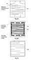
- FIGS. 1A and 1Ba conventional solar cell array is shown.
- a front or glass side 22is illustrated in FIG. 1A
- a back or metal side 24is illustrated in FIG. 1 B.
- various electrical ribbon conductorsidentified with the reference numerals 26 , 28 , 30 and 32 , are connected to the metal side 24 of the solar cell by conventional thermal compression bonding to form a solar cell assembly 34 .
- the solar cell assembly 34is assembled to a substrate 36 , such as an aluminum hollow foil panel carrier, as illustrated in FIG. 3.
- a thermally conductive (but not electrically conductive) epoxyis patterned on the carrier 36 to form a number of interconnection pads 38 , 40 , 42 , and 44 on the substrate 36 .
- the ribbon conductors 26 , 28 and 30 on the solar cell assemblies 34are aligned with the interconnection pads 38 , 40 , 42 and 44 on the carrier 36 .
- the solar cell assembly 34is disposed on the carrier 36 with the electrical ribbon conductors 26 - 32 aligned with the interconnection pads 38 - 44 and secured thereto by thermal compression by way of a wire bonder.
- the wire bonderis in contact with the solar cells 20 during this process. The pressure from the wire bonder is known to short out the solar cells.
- a simplified method for interconnecting solar cell arrayswhich does not damage the solar cells.
- the present inventionrelates to a simplified method and system for interconnecting solar cell arrays which does not utilize cause damage to the solar cells while at the same time minimizing process steps.
- interconnection between solar cellare made by way of a conductive and thermal epoxy (non-electrical epoxy) epoxy, patterned on a substrate.
- the use of the epoxyeliminates the need for wire bonding and isolates the individual cell from electrical shortage, as well as eliminates additional processing steps to interconnect the solar cell arrays.
- FIG. 1Ais a plan view of the glass side of a conventional solar array.
- FIG. 1Bis a plan view of the opposing or metal side of the solar cell array illustrated in FIG. 1 A.
- FIG. 2Aillustrates a number of conventional ribbon conductors.
- FIG. 2Billustrates the ribbon conductors illustrated in FIG. 2A attached to the metal side of the solar cell array illustrated in FIG. 1B forming a solar cell assembly.
- FIG. 3illustrates a conventional aluminum hollow foil panel carrier, with a thermal (non electrically conductive epoxy) applied thereto to form a plurality of interconnection pads.
- FIG. 4illustrates the solar cell assemblies illustrated on FIG. 2B aligned with the carrier illustrated in FIG. 3 .
- FIG. 5illustrates the assembly of the solar cell assemblies to the aluminum hollow foil panel carrier.
- FIG. 6the schematic diagram illustrating the interconnection of solar cell arrays.
- FIGS. 7A-7Hillustrate the process for interconnecting the solar cell arrays in accordance with the present invention.
- FIGS. 8A-8Hillustrate an alternate embodiment of the invention utilizing thick film screening on a printed circuit board for interconnection.
- FIGS. 9A-9Cillustrate on another alternate embodiment of the invention utilizing an etching printed circuit board for interconnection.
- the present inventionrelates to a relatively simple and effective method for interconnecting solar cell arrays which does not utilize wire bonding.
- interconnection of the solar cellsis rather simpler and easier and involves less processing steps, for example, than known interconnection techniques, for example as disclosed in U.S. Pat. No. 5,466,302.
- the system and method for interconnecting the solar cells in accordance with the present inventionis relatively easier to manufacture and thus less expensive.
- FIGS. 7A-7HThree embodiments of the invention are described and illustrated.
- One embodimentis illustrated in FIGS. 7A-7H which involves forming a thick film interconnection pattern on a substrate, such as an aluminum hollow foil panel carrier, and interconnecting the solar cell bond pads to the electrical interconnection pattern by way of an electrically conductive epoxy.
- An alternate embodiment of the inventionis illustrated in FIGS. 8A-8H which involves forming an interconnection pattern on a printed circuit board by film screening techniques.
- FIGS. 9A-9Cinvolves etching the copper on a printed circuit board to form an interconnection pattern and interconnecting the solar cells to the interconnection pattern by way of a conductive epoxy. All three embodiments in accordance with the present invention enable interconnections between solar cell arrays to form a solar cell panel.
- an exemplary solar panelis illustrated and generally identified with the reference numeral 50 .
- the solar panel 50is shown with an exemplary number of solar cell arrays 52 , 54 , 56 , 58 , 60 and 62 .
- Each solar cell array 52 , 54 , 56 , 58 , 60 and 62is formed from an exemplary number of solar cells 64 , 66 , 68 , 70 , 72 , 74 , 76 , 78 and 80 .
- Various techniquesare known for interconnecting individual solar cells, for example, as disclosed in U.S. Pat. Nos.
- each solar cell array 52 - 62is provided with a positive polarity contact, generally identified with the reference numeral 82 , and a negative polarity contact, generally identified with the reference numeral 84 . As shown in FIG.
- multiple solar cell arrays 52 - 62often need to be connected in series for high voltage applications.
- the solar cell pairs 52 / 58 ; 54 / 60 and 56 / 62are shown schematically connected in the series, represented by the arrows 86 , 88 and 90 to form banks of solar cell arrays. 92 , 94 and 96 .
- multiple solar cell array banks 92 , 94 and 96are connected in parallel. These parallel connections are represented by the arrows 98 , 100 , 102 , 104 , 106 , 108 and 110 .
- FIGS. 7A-7Ha process for interconnecting solar cell arrays in accordance with the present invention is illustrated.
- a carrier 112such as, an aluminum hollow foil panel carrier
- the carrier 112is coated with a thermally conductive non-electrically conductive epoxy 114 , such as Ablestik 84 - 3 , as shown in FIG. 7 B.
- a thermally conductive non-electrically conductive epoxy 114such as Ablestik 84 - 3
- Other thermally conductive epoxiesare also suitable; however, the selected epoxy should have a thermal expansion characteristic similar to the thermal expansion characteristic of the glass on the solar cell.
- a thick film electrical interconnection pattern 116is printed on top of the epoxy 114 by industrial standard thick film processing techniques.
- the interconnection pattern 116is formed as generally shown in FIG. 7 C and includes a plurality of spaced apart interconnective rectangular conductors 118 .
- the areas outside of the rectangular conductive areas 118define isolation areas while the area within the conductive pattern conductive rectangles 118 form conductive areas.
- a mask(not shown) is used to pattern the non-conductive areas.
- a non-electrically but thermally conductive epoxy 120for example, Loctite® 3536 or equivalent is injected in the isolation areas as generally shown in FIG. 7 D.
- a mask(not shown) is used to pattern a conductive areas within the conductive rectangles 118 .
- An electrically conductive epoxy 122for example Ablestik® 965-1L or equivalent is injected into the conductive areas as generally shown in FIG. 7 E.
- a solar cell panelgenerally identified with the reference numeral 24 , which consists of a plurality of solar cell arrays, is loaded into a vacuum disk, generally identified with the reference number 126 .
- An exemplary vacuum disk for receiving multiple solar cell panelsis disclosed in U.S. patent application Ser. No. 09/316,991.
- the vacuum disk 126is preferably adapted for multiple solar cell panels with mesa patterns for alignment and epoxy high control. As shown in FIG.
- the vacuum disk loaded with the solar cell panelsis aligned with the carrier 112 and pressed against the carrier 112 .
- the epoxyis allowed to cure.
- the vacuum chuckis removed leaving a solar cell panel with a plurality of interconnected solar cell arrays.
- a non-electrical epoxysuch as Loctite® 3565 or equivalent may be applied along the joint therebetween to secure the solar cell panels to the carrier 112 .
- FIGS. 8A-8HAn alternative embodiment of the invention is illustrated in FIGS. 8A-8H.
- a printed circuit boardis used instead of a non-electrically conductive coating, for example, Rogers Duroid 6002 or equivalent on a hollow aluminum foil carrier as discussed above.
- a solar cell 124for example, as illustrated in FIG. 8A, is adapted to be electrically interconnected with other solar cell arrays by way of interconnection PC board 126 illustrated in FIG. 8 B.
- the process for forming the solar cell interconnection PC board 126is illustrated in FIGS. 8C-8F.
- FIGS. 8G-8Hillustrate the principle of an interconnection PC board for interconnecting multiple solar cell arrays.
- the solar cell array 124is a conventional solar cell array, for example, as supplied by Solarex Corporation of Rockfield, Md.
- the interconnection PC board 126is formed by known thick film screen printing techniques, as discussed above.
- an electrically conductive epoxyfor example, Ablebond® 965-1L or 84-1LMI
- an isolation area 130is screen printed on top of the conductive pattern as generally shown in FIG. 8 D.
- the interconnection patterned formed with the conductive epoxyis formed with a number of rectangles, generally identified with the reference numeral 132 forming conductive areas.
- conductive areas 132are filled with the conductive epoxy as generally shown in FIG. 8 E.
- the solar cell 124is placed on the PC board as shown in FIG. 8 F.
- the conductive pattern 128facilitates connections between solar cell arrays without the need for wire bonding.
- FIGS. 8C-8Fmay be used to form a solar panel using an interconnection PC board 134 .
- the interconnection PC board 134is used to interconnect a plurality of solar cell arrays and facilitate connections of those arrays to other solar cell arrays.
- FIG. 8Hillustrates an assembly of multiple solar cell arrays disposed on a PC board 134 .
- the copper in a PC boardmay be etched in lieu of thick film screening.
- a PC board 140may be masked, by a mask (not shown) to form an interconnection pattern 142 , generally identified with the reference numeral 142 .
- the printed circuit board 140is etched by known techniques to expose the copper and to form the conductive pattern 142 and in particular generally rectangular electrically conductive areas 144 and non-conductive areas 146 .
- the electrically conductive areas 144may be filed with an electrically conductive epoxy, for example, Ablestik® 965-1L or equivalent as shown in FIG.
- a solar cell array 148aligned with the PC board 140 and placed thereon utilizing a vacuum disk as discussed above.
Landscapes
- Photovoltaic Devices (AREA)
Abstract
Description
Claims (12)
Priority Applications (1)
| Application Number | Priority Date | Filing Date | Title |
|---|---|---|---|
| US09/540,735US6294725B1 (en) | 2000-03-31 | 2000-03-31 | Wireless solar cell array electrical interconnection scheme |
Applications Claiming Priority (1)
| Application Number | Priority Date | Filing Date | Title |
|---|---|---|---|
| US09/540,735US6294725B1 (en) | 2000-03-31 | 2000-03-31 | Wireless solar cell array electrical interconnection scheme |
Publications (1)
| Publication Number | Publication Date |
|---|---|
| US6294725B1true US6294725B1 (en) | 2001-09-25 |
Family
ID=24156712
Family Applications (1)
| Application Number | Title | Priority Date | Filing Date |
|---|---|---|---|
| US09/540,735Expired - LifetimeUS6294725B1 (en) | 2000-03-31 | 2000-03-31 | Wireless solar cell array electrical interconnection scheme |
Country Status (1)
| Country | Link |
|---|---|
| US (1) | US6294725B1 (en) |
Cited By (65)
| Publication number | Priority date | Publication date | Assignee | Title |
|---|---|---|---|---|
| US6531653B1 (en)* | 2001-09-11 | 2003-03-11 | The Boeing Company | Low cost high solar flux photovoltaic concentrator receiver |
| US6563040B2 (en)* | 2001-10-11 | 2003-05-13 | Pinnacle West Capital Corporation | Structure for supporting a photovoltaic module in a solar energy collection system |
| US20030127124A1 (en)* | 2002-01-04 | 2003-07-10 | Jones Bernard D. | Solar cell stringing machine |
| US6729081B2 (en)* | 2000-06-09 | 2004-05-04 | United Solar Systems Corporation | Self-adhesive photovoltaic module |
| US6805786B2 (en) | 2002-09-24 | 2004-10-19 | Northrop Grumman Corporation | Precious alloyed metal solder plating process |
| US20070012312A1 (en)* | 2005-07-18 | 2007-01-18 | Arizona Public Service Company | Structure for supporting energy conversion modules and solar energy collection system |
| US20080135090A1 (en)* | 2006-12-11 | 2008-06-12 | Sunmodular, Inc. | Solar roof tiles with heat exchange and methods of making thereof |
| US20080135086A1 (en)* | 2006-12-11 | 2008-06-12 | Sunmodular, Inc. | Photovoltaic cells, modules and methods of making same |
| US20080134497A1 (en)* | 2006-12-11 | 2008-06-12 | Sunmodular, Inc. | Modular solar panels with heat exchange & methods of making thereof |
| US20080210294A1 (en)* | 2006-10-09 | 2008-09-04 | Mehrdad Moslehi | Solar module structures and assembly methods for pyramidal three-dimensional thin-film solar cells |
| US20080236567A1 (en)* | 2007-03-29 | 2008-10-02 | Hayden Herbert T | System for supporting energy conversion modules |
| US20080264477A1 (en)* | 2006-10-09 | 2008-10-30 | Soltaix, Inc. | Methods for manufacturing three-dimensional thin-film solar cells |
| US20080289684A1 (en)* | 2006-10-09 | 2008-11-27 | Soltaix, Inc. | Pyramidal three-dimensional thin-film solar cells |
| US20090301549A1 (en)* | 2006-10-09 | 2009-12-10 | Soltaix, Inc. | Solar module structures and assembly methods for three-dimensional thin-film solar cells |
| US20100024881A1 (en)* | 2006-12-22 | 2010-02-04 | Advent Solar, Inc. | Interconnect Technologies for Back Contact Solar Cells and Modules |
| US20100045265A1 (en)* | 2008-08-19 | 2010-02-25 | Suss Microtec Test Systems Gmbh | Method and device for forming a temporary electrical contact to a solar cell |
| US20100116316A1 (en)* | 2008-11-26 | 2010-05-13 | Solexel, Inc. | Truncated pyramid structures for see-through solar cells |
| US20100144080A1 (en)* | 2008-06-02 | 2010-06-10 | Solexel, Inc. | Method and apparatus to transfer coat uneven surface |
| US20100148318A1 (en)* | 2008-11-13 | 2010-06-17 | Solexel, Inc. | Three-Dimensional Semiconductor Template for Making High Efficiency Thin-Film Solar Cells |
| US20100154998A1 (en)* | 2007-08-17 | 2010-06-24 | Solexel, Inc. | Alternate use for low viscosity liquids and method to gel liquid |
| US20100203711A1 (en)* | 2009-02-06 | 2010-08-12 | Solexel, Inc. | Trench Formation Method For Releasing A Thin-Film Substrate From A Reusable Semiconductor Template |
| US20100267186A1 (en)* | 2008-11-13 | 2010-10-21 | Solexel, Inc. | Method for fabricating a three-dimensional thin-film semiconductor substrate from a template |
| US20100267245A1 (en)* | 2009-04-14 | 2010-10-21 | Solexel, Inc. | High efficiency epitaxial chemical vapor deposition (cvd) reactor |
| US20100279494A1 (en)* | 2006-10-09 | 2010-11-04 | Solexel, Inc. | Method For Releasing a Thin-Film Substrate |
| US20100294356A1 (en)* | 2009-04-24 | 2010-11-25 | Solexel, Inc. | Integrated 3-dimensional and planar metallization structure for thin film solar cells |
| US20100300518A1 (en)* | 2009-05-29 | 2010-12-02 | Solexel, Inc. | Three-dimensional thin-film semiconductor substrate with through-holes and methods of manufacturing |
| US20100304521A1 (en)* | 2006-10-09 | 2010-12-02 | Solexel, Inc. | Shadow Mask Methods For Manufacturing Three-Dimensional Thin-Film Solar Cells |
| US20100304522A1 (en)* | 2009-05-05 | 2010-12-02 | Solexel, Inc. | Ion implantation fabrication process for thin-film crystalline silicon solar cells |
| US20110014742A1 (en)* | 2009-05-22 | 2011-01-20 | Solexel, Inc. | Method of creating reusable template for detachable thin film substrate |
| US20110017282A1 (en)* | 2009-07-24 | 2011-01-27 | Miasole | Energy transfer through coupling from photovoltaic modules |
| WO2011003969A3 (en)* | 2009-07-10 | 2011-04-21 | Eppsteinfoils Gmbh & Co Kg | Composite system for photovoltaic modules |
| US20110120882A1 (en)* | 2009-01-15 | 2011-05-26 | Solexel, Inc. | Porous silicon electro-etching system and method |
| US7989692B2 (en) | 1999-03-30 | 2011-08-02 | Daniel Luch | Substrate and collector grid structures for integrated series connected photovoltaic arrays and process of manufacturing of such arrays |
| US20110203638A1 (en)* | 2009-07-16 | 2011-08-25 | Entech Solar, Inc. | Concentrating linear photovoltaic receiver and method for manufacturing same |
| US20110214712A1 (en)* | 2008-08-06 | 2011-09-08 | Scott Frazier | Solar energy conversion |
| US8110737B2 (en) | 1999-03-30 | 2012-02-07 | Daniel Luch | Collector grid, electrode structures and interrconnect structures for photovoltaic arrays and methods of manufacture |
| US8138413B2 (en) | 2006-04-13 | 2012-03-20 | Daniel Luch | Collector grid and interconnect structures for photovoltaic arrays and modules |
| US8193076B2 (en) | 2006-10-09 | 2012-06-05 | Solexel, Inc. | Method for releasing a thin semiconductor substrate from a reusable template |
| US8198696B2 (en) | 2000-02-04 | 2012-06-12 | Daniel Luch | Substrate structures for integrated series connected photovoltaic arrays and process of manufacture of such arrays |
| US8222513B2 (en) | 2006-04-13 | 2012-07-17 | Daniel Luch | Collector grid, electrode structures and interconnect structures for photovoltaic arrays and methods of manufacture |
| US8241940B2 (en) | 2010-02-12 | 2012-08-14 | Solexel, Inc. | Double-sided reusable template for fabrication of semiconductor substrates for photovoltaic cell and microelectronics device manufacturing |
| US20130019919A1 (en)* | 2011-07-22 | 2013-01-24 | Space Systems/Loral, Inc. | Current collector bar and grid pattern for a photovoltaic solar cell |
| US8399331B2 (en) | 2007-10-06 | 2013-03-19 | Solexel | Laser processing for high-efficiency thin crystalline silicon solar cell fabrication |
| EP1844494A4 (en)* | 2005-01-27 | 2013-10-09 | Transform Solar Pty Ltd | MODULAR SUBASSEMBLY OF SEMICONDUCTOR BANDS |
| US8664030B2 (en) | 1999-03-30 | 2014-03-04 | Daniel Luch | Collector grid and interconnect structures for photovoltaic arrays and modules |
| US8729385B2 (en) | 2006-04-13 | 2014-05-20 | Daniel Luch | Collector grid and interconnect structures for photovoltaic arrays and modules |
| US8822810B2 (en) | 2006-04-13 | 2014-09-02 | Daniel Luch | Collector grid and interconnect structures for photovoltaic arrays and modules |
| US8828517B2 (en) | 2009-03-23 | 2014-09-09 | Solexel, Inc. | Structure and method for improving solar cell efficiency and mechanical strength |
| US8884155B2 (en) | 2006-04-13 | 2014-11-11 | Daniel Luch | Collector grid and interconnect structures for photovoltaic arrays and modules |
| US8906218B2 (en) | 2010-05-05 | 2014-12-09 | Solexel, Inc. | Apparatus and methods for uniformly forming porous semiconductor on a substrate |
| US8946547B2 (en) | 2010-08-05 | 2015-02-03 | Solexel, Inc. | Backplane reinforcement and interconnects for solar cells |
| US8962380B2 (en) | 2009-12-09 | 2015-02-24 | Solexel, Inc. | High-efficiency photovoltaic back-contact solar cell structures and manufacturing methods using thin planar semiconductor absorbers |
| US8999058B2 (en) | 2009-05-05 | 2015-04-07 | Solexel, Inc. | High-productivity porous semiconductor manufacturing equipment |
| US9006563B2 (en) | 2006-04-13 | 2015-04-14 | Solannex, Inc. | Collector grid and interconnect structures for photovoltaic arrays and modules |
| US9076642B2 (en) | 2009-01-15 | 2015-07-07 | Solexel, Inc. | High-Throughput batch porous silicon manufacturing equipment design and processing methods |
| US9200452B2 (en) | 2012-09-20 | 2015-12-01 | Mbc Ventures, Inc. | Controller for skylight energy management system |
| US9236512B2 (en) | 2006-04-13 | 2016-01-12 | Daniel Luch | Collector grid and interconnect structures for photovoltaic arrays and modules |
| US9318644B2 (en) | 2009-05-05 | 2016-04-19 | Solexel, Inc. | Ion implantation and annealing for thin film crystalline solar cells |
| US9508886B2 (en) | 2007-10-06 | 2016-11-29 | Solexel, Inc. | Method for making a crystalline silicon solar cell substrate utilizing flat top laser beam |
| US9627565B2 (en) | 2013-11-27 | 2017-04-18 | Space Systems/Loral, Llc | Integral corner bypass diode interconnecting configuration for multiple solar cells |
| US9722115B2 (en) | 2012-12-26 | 2017-08-01 | Industrial Technology Research Institute | Solar cell encapsulating module and method for manufacturing the same |
| US9748414B2 (en) | 2011-05-20 | 2017-08-29 | Arthur R. Zingher | Self-activated front surface bias for a solar cell |
| US9865758B2 (en) | 2006-04-13 | 2018-01-09 | Daniel Luch | Collector grid and interconnect structures for photovoltaic arrays and modules |
| US9870937B2 (en) | 2010-06-09 | 2018-01-16 | Ob Realty, Llc | High productivity deposition reactor comprising a gas flow chamber having a tapered gas flow space |
| CN109155342A (en)* | 2016-05-23 | 2019-01-04 | 株式会社钟化 | Solar cell, method for manufacturing the same, and solar cell panel |
Citations (20)
| Publication number | Priority date | Publication date | Assignee | Title |
|---|---|---|---|---|
| US4084985A (en)* | 1977-04-25 | 1978-04-18 | The United States Of America As Represented By The Administrator Of The National Aeronautics And Space Administration | Method for producing solar energy panels by automation |
| US4240842A (en) | 1979-03-28 | 1980-12-23 | Solarex Corporation | Solar cell having contacts and antireflective coating |
| US4348254A (en) | 1978-12-27 | 1982-09-07 | Solarex Corporation | Method of making solar cell |
| US4392010A (en) | 1979-01-16 | 1983-07-05 | Solarex Corporation | Photovoltaic cells having contacts and method of applying same |
| US4562637A (en)* | 1983-06-22 | 1986-01-07 | Hitachi, Ltd. | Method of manufacturing solar battery |
| US4892592A (en) | 1987-03-26 | 1990-01-09 | Solarex Corporation | Thin film semiconductor solar cell array and method of making |
| US5006179A (en) | 1989-05-24 | 1991-04-09 | Solarex Corporation | Interconnect for electrically connecting solar cells |
| US5011544A (en) | 1989-09-08 | 1991-04-30 | Solarex Corporation | Solar panel with interconnects and masking structure, and method |
| US5021099A (en) | 1988-08-09 | 1991-06-04 | The Boeing Company | Solar cell interconnection and packaging using tape carrier |
| US5125983A (en)* | 1991-04-22 | 1992-06-30 | Electric Power Research Institute, Inc. | Generating electric power from solar radiation |
| US5246506A (en) | 1991-07-16 | 1993-09-21 | Solarex Corporation | Multijunction photovoltaic device and fabrication method |
| US5460659A (en)* | 1993-12-10 | 1995-10-24 | Spectrolab, Inc. | Concentrating photovoltaic module and fabrication method |
| US5466302A (en) | 1994-05-09 | 1995-11-14 | Regents Of The University Of California | Solar cell array interconnects |
| US5620528A (en) | 1994-09-30 | 1997-04-15 | Siemens Solar Gmbh | Solar cell with a connecting structure |
| US5922142A (en) | 1996-11-07 | 1999-07-13 | Midwest Research Institute | Photovoltaic devices comprising cadmium stannate transparent conducting films and method for making |
| US5928437A (en) | 1995-02-09 | 1999-07-27 | The Boeing Company | Microarray for efficient energy generation for satellites |
| US5951786A (en)* | 1997-12-19 | 1999-09-14 | Sandia Corporation | Laminated photovoltaic modules using back-contact solar cells |
| US5963790A (en) | 1992-07-22 | 1999-10-05 | Mitsubshiki Denki Kabushiki Kaisha | Method of producing thin film solar cell |
| US5961737A (en) | 1996-12-12 | 1999-10-05 | Hughes Electronics Corporation | Welded wire termination device and method for constructing a solar array |
| US6130465A (en)* | 1997-10-29 | 2000-10-10 | Light Point Systems Inc. | Micro-solar assembly |
- 2000
- 2000-03-31USUS09/540,735patent/US6294725B1/ennot_activeExpired - Lifetime
Patent Citations (20)
| Publication number | Priority date | Publication date | Assignee | Title |
|---|---|---|---|---|
| US4084985A (en)* | 1977-04-25 | 1978-04-18 | The United States Of America As Represented By The Administrator Of The National Aeronautics And Space Administration | Method for producing solar energy panels by automation |
| US4348254A (en) | 1978-12-27 | 1982-09-07 | Solarex Corporation | Method of making solar cell |
| US4392010A (en) | 1979-01-16 | 1983-07-05 | Solarex Corporation | Photovoltaic cells having contacts and method of applying same |
| US4240842A (en) | 1979-03-28 | 1980-12-23 | Solarex Corporation | Solar cell having contacts and antireflective coating |
| US4562637A (en)* | 1983-06-22 | 1986-01-07 | Hitachi, Ltd. | Method of manufacturing solar battery |
| US4892592A (en) | 1987-03-26 | 1990-01-09 | Solarex Corporation | Thin film semiconductor solar cell array and method of making |
| US5021099A (en) | 1988-08-09 | 1991-06-04 | The Boeing Company | Solar cell interconnection and packaging using tape carrier |
| US5006179A (en) | 1989-05-24 | 1991-04-09 | Solarex Corporation | Interconnect for electrically connecting solar cells |
| US5011544A (en) | 1989-09-08 | 1991-04-30 | Solarex Corporation | Solar panel with interconnects and masking structure, and method |
| US5125983A (en)* | 1991-04-22 | 1992-06-30 | Electric Power Research Institute, Inc. | Generating electric power from solar radiation |
| US5246506A (en) | 1991-07-16 | 1993-09-21 | Solarex Corporation | Multijunction photovoltaic device and fabrication method |
| US5963790A (en) | 1992-07-22 | 1999-10-05 | Mitsubshiki Denki Kabushiki Kaisha | Method of producing thin film solar cell |
| US5460659A (en)* | 1993-12-10 | 1995-10-24 | Spectrolab, Inc. | Concentrating photovoltaic module and fabrication method |
| US5466302A (en) | 1994-05-09 | 1995-11-14 | Regents Of The University Of California | Solar cell array interconnects |
| US5620528A (en) | 1994-09-30 | 1997-04-15 | Siemens Solar Gmbh | Solar cell with a connecting structure |
| US5928437A (en) | 1995-02-09 | 1999-07-27 | The Boeing Company | Microarray for efficient energy generation for satellites |
| US5922142A (en) | 1996-11-07 | 1999-07-13 | Midwest Research Institute | Photovoltaic devices comprising cadmium stannate transparent conducting films and method for making |
| US5961737A (en) | 1996-12-12 | 1999-10-05 | Hughes Electronics Corporation | Welded wire termination device and method for constructing a solar array |
| US6130465A (en)* | 1997-10-29 | 2000-10-10 | Light Point Systems Inc. | Micro-solar assembly |
| US5951786A (en)* | 1997-12-19 | 1999-09-14 | Sandia Corporation | Laminated photovoltaic modules using back-contact solar cells |
Cited By (104)
| Publication number | Priority date | Publication date | Assignee | Title |
|---|---|---|---|---|
| US7989693B2 (en) | 1999-03-30 | 2011-08-02 | Daniel Luch | Substrate and collector grid structures for integrated series connected photovoltaic arrays and process of manufacture of such arrays |
| US8304646B2 (en) | 1999-03-30 | 2012-11-06 | Daniel Luch | Substrate and collector grid structures for integrated series connected photovoltaic arrays and process of manufacture of such arrays |
| US7989692B2 (en) | 1999-03-30 | 2011-08-02 | Daniel Luch | Substrate and collector grid structures for integrated series connected photovoltaic arrays and process of manufacturing of such arrays |
| US8110737B2 (en) | 1999-03-30 | 2012-02-07 | Daniel Luch | Collector grid, electrode structures and interrconnect structures for photovoltaic arrays and methods of manufacture |
| US8664030B2 (en) | 1999-03-30 | 2014-03-04 | Daniel Luch | Collector grid and interconnect structures for photovoltaic arrays and modules |
| US8198696B2 (en) | 2000-02-04 | 2012-06-12 | Daniel Luch | Substrate structures for integrated series connected photovoltaic arrays and process of manufacture of such arrays |
| US6729081B2 (en)* | 2000-06-09 | 2004-05-04 | United Solar Systems Corporation | Self-adhesive photovoltaic module |
| US6531653B1 (en)* | 2001-09-11 | 2003-03-11 | The Boeing Company | Low cost high solar flux photovoltaic concentrator receiver |
| WO2003031879A3 (en)* | 2001-10-11 | 2009-06-18 | Pinnacle West Capital Corp | Structure for supporting a photovoltaic module in a solar energy collection system |
| US6563040B2 (en)* | 2001-10-11 | 2003-05-13 | Pinnacle West Capital Corporation | Structure for supporting a photovoltaic module in a solar energy collection system |
| US6841728B2 (en) | 2002-01-04 | 2005-01-11 | G.T. Equipment Technologies, Inc. | Solar cell stringing machine |
| US20030127124A1 (en)* | 2002-01-04 | 2003-07-10 | Jones Bernard D. | Solar cell stringing machine |
| US6805786B2 (en) | 2002-09-24 | 2004-10-19 | Northrop Grumman Corporation | Precious alloyed metal solder plating process |
| EP1844494A4 (en)* | 2005-01-27 | 2013-10-09 | Transform Solar Pty Ltd | MODULAR SUBASSEMBLY OF SEMICONDUCTOR BANDS |
| US20070012312A1 (en)* | 2005-07-18 | 2007-01-18 | Arizona Public Service Company | Structure for supporting energy conversion modules and solar energy collection system |
| US20070215145A1 (en)* | 2005-07-18 | 2007-09-20 | Arizona Public Service Company | System for Supporting Energy Conversion Modules |
| US7252083B2 (en) | 2005-07-18 | 2007-08-07 | Arizona Public Service Company | Structure for supporting energy conversion modules and solar energy collection system |
| US8138413B2 (en) | 2006-04-13 | 2012-03-20 | Daniel Luch | Collector grid and interconnect structures for photovoltaic arrays and modules |
| US8222513B2 (en) | 2006-04-13 | 2012-07-17 | Daniel Luch | Collector grid, electrode structures and interconnect structures for photovoltaic arrays and methods of manufacture |
| US8729385B2 (en) | 2006-04-13 | 2014-05-20 | Daniel Luch | Collector grid and interconnect structures for photovoltaic arrays and modules |
| US8822810B2 (en) | 2006-04-13 | 2014-09-02 | Daniel Luch | Collector grid and interconnect structures for photovoltaic arrays and modules |
| US8884155B2 (en) | 2006-04-13 | 2014-11-11 | Daniel Luch | Collector grid and interconnect structures for photovoltaic arrays and modules |
| US9006563B2 (en) | 2006-04-13 | 2015-04-14 | Solannex, Inc. | Collector grid and interconnect structures for photovoltaic arrays and modules |
| US9236512B2 (en) | 2006-04-13 | 2016-01-12 | Daniel Luch | Collector grid and interconnect structures for photovoltaic arrays and modules |
| US9865758B2 (en) | 2006-04-13 | 2018-01-09 | Daniel Luch | Collector grid and interconnect structures for photovoltaic arrays and modules |
| US9397250B2 (en) | 2006-10-09 | 2016-07-19 | Solexel, Inc. | Releasing apparatus for separating a semiconductor substrate from a semiconductor template |
| US8512581B2 (en) | 2006-10-09 | 2013-08-20 | Solexel, Inc. | Methods for liquid transfer coating of three-dimensional substrates |
| US8193076B2 (en) | 2006-10-09 | 2012-06-05 | Solexel, Inc. | Method for releasing a thin semiconductor substrate from a reusable template |
| US9349887B2 (en) | 2006-10-09 | 2016-05-24 | Solexel, Inc. | Three-dimensional thin-film solar cells |
| US8293558B2 (en) | 2006-10-09 | 2012-10-23 | Solexel, Inc. | Method for releasing a thin-film substrate |
| US8035027B2 (en)* | 2006-10-09 | 2011-10-11 | Solexel, Inc. | Solar module structures and assembly methods for pyramidal three-dimensional thin-film solar cells |
| US8035028B2 (en) | 2006-10-09 | 2011-10-11 | Solexel, Inc. | Pyramidal three-dimensional thin-film solar cells |
| US20150068583A1 (en)* | 2006-10-09 | 2015-03-12 | Solexel, Inc. | Solar module structures and assembly methods for three-dimensional thin-film solar cells |
| US20100279494A1 (en)* | 2006-10-09 | 2010-11-04 | Solexel, Inc. | Method For Releasing a Thin-Film Substrate |
| US20090301549A1 (en)* | 2006-10-09 | 2009-12-10 | Soltaix, Inc. | Solar module structures and assembly methods for three-dimensional thin-film solar cells |
| US20090107545A1 (en)* | 2006-10-09 | 2009-04-30 | Soltaix, Inc. | Template for pyramidal three-dimensional thin-film solar cell manufacturing and methods of use |
| US20100304521A1 (en)* | 2006-10-09 | 2010-12-02 | Solexel, Inc. | Shadow Mask Methods For Manufacturing Three-Dimensional Thin-Film Solar Cells |
| US20080289684A1 (en)* | 2006-10-09 | 2008-11-27 | Soltaix, Inc. | Pyramidal three-dimensional thin-film solar cells |
| US20080264477A1 (en)* | 2006-10-09 | 2008-10-30 | Soltaix, Inc. | Methods for manufacturing three-dimensional thin-film solar cells |
| US7999174B2 (en) | 2006-10-09 | 2011-08-16 | Solexel, Inc. | Solar module structures and assembly methods for three-dimensional thin-film solar cells |
| US20080210294A1 (en)* | 2006-10-09 | 2008-09-04 | Mehrdad Moslehi | Solar module structures and assembly methods for pyramidal three-dimensional thin-film solar cells |
| US20080135086A1 (en)* | 2006-12-11 | 2008-06-12 | Sunmodular, Inc. | Photovoltaic cells, modules and methods of making same |
| US7728219B2 (en) | 2006-12-11 | 2010-06-01 | Sunmodular, Inc. | Photovoltaic cells, modules and methods of making same |
| US20080135094A1 (en)* | 2006-12-11 | 2008-06-12 | Sunmodular, Inc. | Photovoltaic roof tiles and methods of making same |
| US8410350B2 (en) | 2006-12-11 | 2013-04-02 | Ns Acquisition Llc | Modular solar panels with heat exchange |
| US20080135090A1 (en)* | 2006-12-11 | 2008-06-12 | Sunmodular, Inc. | Solar roof tiles with heat exchange and methods of making thereof |
| US20080134497A1 (en)* | 2006-12-11 | 2008-06-12 | Sunmodular, Inc. | Modular solar panels with heat exchange & methods of making thereof |
| US20080135088A1 (en)* | 2006-12-11 | 2008-06-12 | Sunmodular, Inc. | Interlocking solar roof tiles with heat exchange |
| US20100024881A1 (en)* | 2006-12-22 | 2010-02-04 | Advent Solar, Inc. | Interconnect Technologies for Back Contact Solar Cells and Modules |
| US20080236567A1 (en)* | 2007-03-29 | 2008-10-02 | Hayden Herbert T | System for supporting energy conversion modules |
| US7647924B2 (en) | 2007-03-29 | 2010-01-19 | Arizona Public Service Company | System for supporting energy conversion modules |
| US20100154998A1 (en)* | 2007-08-17 | 2010-06-24 | Solexel, Inc. | Alternate use for low viscosity liquids and method to gel liquid |
| US8399331B2 (en) | 2007-10-06 | 2013-03-19 | Solexel | Laser processing for high-efficiency thin crystalline silicon solar cell fabrication |
| US9508886B2 (en) | 2007-10-06 | 2016-11-29 | Solexel, Inc. | Method for making a crystalline silicon solar cell substrate utilizing flat top laser beam |
| US20100144080A1 (en)* | 2008-06-02 | 2010-06-10 | Solexel, Inc. | Method and apparatus to transfer coat uneven surface |
| US20110214712A1 (en)* | 2008-08-06 | 2011-09-08 | Scott Frazier | Solar energy conversion |
| US9217582B2 (en)* | 2008-08-06 | 2015-12-22 | Mbc Ventures, Inc. | Solar energy conversion |
| CN102792104B (en)* | 2008-08-06 | 2015-01-21 | Mbc合资有限公司 | Solar energy conversion |
| US20100045265A1 (en)* | 2008-08-19 | 2010-02-25 | Suss Microtec Test Systems Gmbh | Method and device for forming a temporary electrical contact to a solar cell |
| US8168465B2 (en) | 2008-11-13 | 2012-05-01 | Solexel, Inc. | Three-dimensional semiconductor template for making high efficiency thin-film solar cells |
| US8288195B2 (en) | 2008-11-13 | 2012-10-16 | Solexel, Inc. | Method for fabricating a three-dimensional thin-film semiconductor substrate from a template |
| US20100148318A1 (en)* | 2008-11-13 | 2010-06-17 | Solexel, Inc. | Three-Dimensional Semiconductor Template for Making High Efficiency Thin-Film Solar Cells |
| US20100148319A1 (en)* | 2008-11-13 | 2010-06-17 | Solexel, Inc. | Substrates for High-Efficiency Thin-Film Solar Cells Based on Crystalline Templates |
| US8294026B2 (en) | 2008-11-13 | 2012-10-23 | Solexel, Inc. | High-efficiency thin-film solar cells |
| US20100267186A1 (en)* | 2008-11-13 | 2010-10-21 | Solexel, Inc. | Method for fabricating a three-dimensional thin-film semiconductor substrate from a template |
| US8664737B2 (en) | 2008-11-13 | 2014-03-04 | Selexel, Inc. | Three-dimensional semiconductor template for making high efficiency thin-film solar cells |
| US8053665B2 (en) | 2008-11-26 | 2011-11-08 | Solexel, Inc. | Truncated pyramid structures for see-through solar cells |
| US20100116316A1 (en)* | 2008-11-26 | 2010-05-13 | Solexel, Inc. | Truncated pyramid structures for see-through solar cells |
| US9076642B2 (en) | 2009-01-15 | 2015-07-07 | Solexel, Inc. | High-Throughput batch porous silicon manufacturing equipment design and processing methods |
| US20110120882A1 (en)* | 2009-01-15 | 2011-05-26 | Solexel, Inc. | Porous silicon electro-etching system and method |
| US8926803B2 (en) | 2009-01-15 | 2015-01-06 | Solexel, Inc. | Porous silicon electro-etching system and method |
| US10829864B2 (en) | 2009-01-15 | 2020-11-10 | Trutag Technologies, Inc. | Apparatus and methods for uniformly forming porous semiconductor on a substrate |
| US20100203711A1 (en)* | 2009-02-06 | 2010-08-12 | Solexel, Inc. | Trench Formation Method For Releasing A Thin-Film Substrate From A Reusable Semiconductor Template |
| US8278192B2 (en) | 2009-02-06 | 2012-10-02 | Solexel | Trench formation method for releasing a thin-film substrate from a reusable semiconductor template |
| US8828517B2 (en) | 2009-03-23 | 2014-09-09 | Solexel, Inc. | Structure and method for improving solar cell efficiency and mechanical strength |
| US8656860B2 (en) | 2009-04-14 | 2014-02-25 | Solexel, Inc. | High efficiency epitaxial chemical vapor deposition (CVD) reactor |
| US20100267245A1 (en)* | 2009-04-14 | 2010-10-21 | Solexel, Inc. | High efficiency epitaxial chemical vapor deposition (cvd) reactor |
| US9099584B2 (en) | 2009-04-24 | 2015-08-04 | Solexel, Inc. | Integrated three-dimensional and planar metallization structure for thin film solar cells |
| US20100294356A1 (en)* | 2009-04-24 | 2010-11-25 | Solexel, Inc. | Integrated 3-dimensional and planar metallization structure for thin film solar cells |
| US9318644B2 (en) | 2009-05-05 | 2016-04-19 | Solexel, Inc. | Ion implantation and annealing for thin film crystalline solar cells |
| US8999058B2 (en) | 2009-05-05 | 2015-04-07 | Solexel, Inc. | High-productivity porous semiconductor manufacturing equipment |
| US8420435B2 (en) | 2009-05-05 | 2013-04-16 | Solexel, Inc. | Ion implantation fabrication process for thin-film crystalline silicon solar cells |
| US20100304522A1 (en)* | 2009-05-05 | 2010-12-02 | Solexel, Inc. | Ion implantation fabrication process for thin-film crystalline silicon solar cells |
| US8445314B2 (en) | 2009-05-22 | 2013-05-21 | Solexel, Inc. | Method of creating reusable template for detachable thin film substrate |
| US20110014742A1 (en)* | 2009-05-22 | 2011-01-20 | Solexel, Inc. | Method of creating reusable template for detachable thin film substrate |
| US20100300518A1 (en)* | 2009-05-29 | 2010-12-02 | Solexel, Inc. | Three-dimensional thin-film semiconductor substrate with through-holes and methods of manufacturing |
| US8551866B2 (en) | 2009-05-29 | 2013-10-08 | Solexel, Inc. | Three-dimensional thin-film semiconductor substrate with through-holes and methods of manufacturing |
| WO2011003969A3 (en)* | 2009-07-10 | 2011-04-21 | Eppsteinfoils Gmbh & Co Kg | Composite system for photovoltaic modules |
| US20110203638A1 (en)* | 2009-07-16 | 2011-08-25 | Entech Solar, Inc. | Concentrating linear photovoltaic receiver and method for manufacturing same |
| US20110017282A1 (en)* | 2009-07-24 | 2011-01-27 | Miasole | Energy transfer through coupling from photovoltaic modules |
| US8962380B2 (en) | 2009-12-09 | 2015-02-24 | Solexel, Inc. | High-efficiency photovoltaic back-contact solar cell structures and manufacturing methods using thin planar semiconductor absorbers |
| US9401276B2 (en) | 2010-02-12 | 2016-07-26 | Solexel, Inc. | Apparatus for forming porous silicon layers on at least two surfaces of a plurality of silicon templates |
| US8241940B2 (en) | 2010-02-12 | 2012-08-14 | Solexel, Inc. | Double-sided reusable template for fabrication of semiconductor substrates for photovoltaic cell and microelectronics device manufacturing |
| US8906218B2 (en) | 2010-05-05 | 2014-12-09 | Solexel, Inc. | Apparatus and methods for uniformly forming porous semiconductor on a substrate |
| US9870937B2 (en) | 2010-06-09 | 2018-01-16 | Ob Realty, Llc | High productivity deposition reactor comprising a gas flow chamber having a tapered gas flow space |
| US8946547B2 (en) | 2010-08-05 | 2015-02-03 | Solexel, Inc. | Backplane reinforcement and interconnects for solar cells |
| US9748414B2 (en) | 2011-05-20 | 2017-08-29 | Arthur R. Zingher | Self-activated front surface bias for a solar cell |
| US9000288B2 (en)* | 2011-07-22 | 2015-04-07 | Space Systems/Loral, Llc | Current collector bar and grid pattern for a photovoltaic solar cell |
| US20130019919A1 (en)* | 2011-07-22 | 2013-01-24 | Space Systems/Loral, Inc. | Current collector bar and grid pattern for a photovoltaic solar cell |
| US9200452B2 (en) | 2012-09-20 | 2015-12-01 | Mbc Ventures, Inc. | Controller for skylight energy management system |
| US9722115B2 (en) | 2012-12-26 | 2017-08-01 | Industrial Technology Research Institute | Solar cell encapsulating module and method for manufacturing the same |
| US9627565B2 (en) | 2013-11-27 | 2017-04-18 | Space Systems/Loral, Llc | Integral corner bypass diode interconnecting configuration for multiple solar cells |
| CN109155342A (en)* | 2016-05-23 | 2019-01-04 | 株式会社钟化 | Solar cell, method for manufacturing the same, and solar cell panel |
| US20190109253A1 (en)* | 2016-05-23 | 2019-04-11 | Kaneka Corporation | Solar cell and method for manufacturing same, and solar cell panel |
Similar Documents
| Publication | Publication Date | Title |
|---|---|---|
| US6294725B1 (en) | Wireless solar cell array electrical interconnection scheme | |
| US5133810A (en) | Flexible photovoltaic device and manufacturing method thereof | |
| US3553030A (en) | Radiation-sensitive semiconductor device | |
| JP3694252B2 (en) | Lightweight solar cell module | |
| CN103474493B (en) | Encapsulated layer is applied to the photovoltaic module backboard comprising back-contact battery | |
| US9368651B2 (en) | Buss bar strip | |
| US5185042A (en) | Generic solar cell array using a printed circuit substrate | |
| US6353175B1 (en) | Two-terminal cell-interconnected-circuits using mechanically-stacked photovoltaic cells for line-focus concentrator arrays | |
| KR101152010B1 (en) | Solar battery module substrate and solar battery module | |
| US3562020A (en) | Solar cell assembly | |
| US4227298A (en) | Method for interconnecting photovoltaic devices | |
| US12244265B2 (en) | Wiring for a rigid panel solar array | |
| US20090256254A1 (en) | Wafer level interconnection and method | |
| WO1989005521A1 (en) | Solar cell panel | |
| WO2008121293A2 (en) | Solar module manufacturing processes | |
| CN111095789A (en) | Interconnection method of laminated photovoltaic cells | |
| EP3297042A1 (en) | Power routing module with a switching matrix for a solar cell array | |
| JPS60240171A (en) | Solar electric generator | |
| US6248949B1 (en) | Method of manufacturing a solar cell receiver plate of a concentrator photovoltaic array | |
| US4131755A (en) | Interconnection for photovoltaic device array | |
| EP0189976A2 (en) | Extremely lightweight, flexible semiconductor device arrays and method of making same | |
| JP2005191125A (en) | Connection tab for solar cell element connection, solar cell module, and method for manufacturing solar cell module | |
| JPH0567017U (en) | Solar cell module | |
| JPS6230507B2 (en) | ||
| CN110364576B (en) | Solar device with insulating interconnects |
Legal Events
| Date | Code | Title | Description |
|---|---|---|---|
| AS | Assignment | Owner name:TRW INC., CALIFORNIA Free format text:ASSIGNMENT OF ASSIGNORS INTEREST;ASSIGNORS:HIRSCHBERG, ALAN M.;TRAN, DEAN;CARBERRY, DAVID M.;REEL/FRAME:010670/0160;SIGNING DATES FROM 20000323 TO 20000330 | |
| STCF | Information on status: patent grant | Free format text:PATENTED CASE | |
| AS | Assignment | Owner name:NORTHROP GRUMMAN CORPORATION, CALIFORNIA Free format text:ASSIGNMENT OF ASSIGNORS INTEREST;ASSIGNOR:TRW, INC. N/K/A NORTHROP GRUMMAN SPACE AND MISSION SYSTEMS CORPORATION, AN OHIO CORPORATION;REEL/FRAME:013751/0849 Effective date:20030122 Owner name:NORTHROP GRUMMAN CORPORATION,CALIFORNIA Free format text:ASSIGNMENT OF ASSIGNORS INTEREST;ASSIGNOR:TRW, INC. N/K/A NORTHROP GRUMMAN SPACE AND MISSION SYSTEMS CORPORATION, AN OHIO CORPORATION;REEL/FRAME:013751/0849 Effective date:20030122 | |
| FEPP | Fee payment procedure | Free format text:PAYOR NUMBER ASSIGNED (ORIGINAL EVENT CODE: ASPN); ENTITY STATUS OF PATENT OWNER: LARGE ENTITY | |
| FPAY | Fee payment | Year of fee payment:4 | |
| FEPP | Fee payment procedure | Free format text:PAYOR NUMBER ASSIGNED (ORIGINAL EVENT CODE: ASPN); ENTITY STATUS OF PATENT OWNER: LARGE ENTITY Free format text:PAYER NUMBER DE-ASSIGNED (ORIGINAL EVENT CODE: RMPN); ENTITY STATUS OF PATENT OWNER: LARGE ENTITY | |
| FPAY | Fee payment | Year of fee payment:8 | |
| AS | Assignment | Owner name:NORTHROP GRUMMAN SPACE & MISSION SYSTEMS CORP.,CAL Free format text:ASSIGNMENT OF ASSIGNORS INTEREST;ASSIGNOR:NORTHROP GRUMMAN CORPORTION;REEL/FRAME:023699/0551 Effective date:20091125 Owner name:NORTHROP GRUMMAN SPACE & MISSION SYSTEMS CORP., CA Free format text:ASSIGNMENT OF ASSIGNORS INTEREST;ASSIGNOR:NORTHROP GRUMMAN CORPORTION;REEL/FRAME:023699/0551 Effective date:20091125 | |
| AS | Assignment | Owner name:NORTHROP GRUMMAN SYSTEMS CORPORATION,CALIFORNIA Free format text:ASSIGNMENT OF ASSIGNORS INTEREST;ASSIGNOR:NORTHROP GRUMMAN SPACE & MISSION SYSTEMS CORP.;REEL/FRAME:023915/0446 Effective date:20091210 Owner name:NORTHROP GRUMMAN SYSTEMS CORPORATION, CALIFORNIA Free format text:ASSIGNMENT OF ASSIGNORS INTEREST;ASSIGNOR:NORTHROP GRUMMAN SPACE & MISSION SYSTEMS CORP.;REEL/FRAME:023915/0446 Effective date:20091210 | |
| FPAY | Fee payment | Year of fee payment:12 |