US6294470B1 - Slurry-less chemical-mechanical polishing - Google Patents
Slurry-less chemical-mechanical polishingDownload PDFInfo
- Publication number
- US6294470B1 US6294470B1US09/469,922US46992299AUS6294470B1US 6294470 B1US6294470 B1US 6294470B1US 46992299 AUS46992299 AUS 46992299AUS 6294470 B1US6294470 B1US 6294470B1
- Authority
- US
- United States
- Prior art keywords
- oxide
- substrate
- liquid medium
- polishing
- polyelectrolyte
- Prior art date
- Legal status (The legal status is an assumption and is not a legal conclusion. Google has not performed a legal analysis and makes no representation as to the accuracy of the status listed.)
- Expired - Lifetime
Links
- 238000005498polishingMethods0.000titleclaimsabstractdescription39
- 238000000034methodMethods0.000claimsabstractdescription57
- 239000000463materialSubstances0.000claimsabstractdescription47
- 239000000758substrateSubstances0.000claimsabstractdescription38
- 239000007788liquidSubstances0.000claimsabstractdescription26
- 229920000867polyelectrolytePolymers0.000claimsabstractdescription22
- 238000007517polishing processMethods0.000claimsabstractdescription12
- 229910052751metalInorganic materials0.000claimsdescription25
- 239000002184metalSubstances0.000claimsdescription25
- 229920002125Sokalan®Polymers0.000claimsdescription4
- 239000004584polyacrylic acidSubstances0.000claimsdescription4
- 239000000203mixtureSubstances0.000claimsdescription3
- 229920002845Poly(methacrylic acid)Polymers0.000claimsdescription2
- 229920002873PolyethyleniminePolymers0.000claimsdescription2
- 229920003229poly(methyl methacrylate)Polymers0.000claimsdescription2
- 229920001444polymaleic acidPolymers0.000claimsdescription2
- 239000004926polymethyl methacrylateSubstances0.000claimsdescription2
- 239000003082abrasive agentSubstances0.000claims1
- 239000011230binding agentSubstances0.000claims1
- 150000004767nitridesChemical class0.000claims1
- 239000003989dielectric materialSubstances0.000abstractdescription12
- 238000001514detection methodMethods0.000abstractdescription4
- 230000008030eliminationEffects0.000abstract1
- 238000003379elimination reactionMethods0.000abstract1
- VYPSYNLAJGMNEJ-UHFFFAOYSA-NSilicium dioxideChemical compoundO=[Si]=OVYPSYNLAJGMNEJ-UHFFFAOYSA-N0.000description15
- 239000002609mediumSubstances0.000description15
- 238000002955isolationMethods0.000description8
- 229910052814silicon oxideInorganic materials0.000description8
- 230000015572biosynthetic processEffects0.000description5
- 238000005229chemical vapour depositionMethods0.000description5
- 239000000377silicon dioxideSubstances0.000description4
- ZOXJGFHDIHLPTG-UHFFFAOYSA-NBoronChemical compound[B]ZOXJGFHDIHLPTG-UHFFFAOYSA-N0.000description3
- 229910052796boronInorganic materials0.000description3
- 238000012876topographyMethods0.000description3
- RYGMFSIKBFXOCR-UHFFFAOYSA-NCopperChemical compound[Cu]RYGMFSIKBFXOCR-UHFFFAOYSA-N0.000description2
- BOTDANWDWHJENH-UHFFFAOYSA-NTetraethyl orthosilicateChemical compoundCCO[Si](OCC)(OCC)OCCBOTDANWDWHJENH-UHFFFAOYSA-N0.000description2
- 229910052782aluminiumInorganic materials0.000description2
- XAGFODPZIPBFFR-UHFFFAOYSA-NaluminiumChemical compound[Al]XAGFODPZIPBFFR-UHFFFAOYSA-N0.000description2
- 229910052802copperInorganic materials0.000description2
- 239000010949copperSubstances0.000description2
- 238000005516engineering processMethods0.000description2
- 239000012212insulatorSubstances0.000description2
- 238000004519manufacturing processMethods0.000description2
- 238000001020plasma etchingMethods0.000description2
- 239000004065semiconductorSubstances0.000description2
- 235000012239silicon dioxideNutrition0.000description2
- 229910000838Al alloyInorganic materials0.000description1
- VHUUQVKOLVNVRT-UHFFFAOYSA-NAmmonium hydroxideChemical compound[NH4+].[OH-]VHUUQVKOLVNVRT-UHFFFAOYSA-N0.000description1
- 229910000881Cu alloyInorganic materials0.000description1
- BPQQTUXANYXVAA-UHFFFAOYSA-NOrthosilicateChemical compound[O-][Si]([O-])([O-])[O-]BPQQTUXANYXVAA-UHFFFAOYSA-N0.000description1
- CBENFWSGALASAD-UHFFFAOYSA-NOzoneChemical compound[O-][O+]=OCBENFWSGALASAD-UHFFFAOYSA-N0.000description1
- OAICVXFJPJFONN-UHFFFAOYSA-NPhosphorusChemical compound[P]OAICVXFJPJFONN-UHFFFAOYSA-N0.000description1
- 229910052581Si3N4Inorganic materials0.000description1
- RTAQQCXQSZGOHL-UHFFFAOYSA-NTitaniumChemical compound[Ti]RTAQQCXQSZGOHL-UHFFFAOYSA-N0.000description1
- NRTOMJZYCJJWKI-UHFFFAOYSA-NTitanium nitrideChemical compound[Ti]#NNRTOMJZYCJJWKI-UHFFFAOYSA-N0.000description1
- 230000002411adverseEffects0.000description1
- 239000000908ammonium hydroxideSubstances0.000description1
- 239000012736aqueous mediumSubstances0.000description1
- 229910052785arsenicInorganic materials0.000description1
- RQNWIZPPADIBDY-UHFFFAOYSA-Narsenic atomChemical compound[As]RQNWIZPPADIBDY-UHFFFAOYSA-N0.000description1
- QVGXLLKOCUKJST-UHFFFAOYSA-Natomic oxygenChemical compound[O]QVGXLLKOCUKJST-UHFFFAOYSA-N0.000description1
- 239000011248coating agentSubstances0.000description1
- 238000000576coating methodMethods0.000description1
- 229910052681coesiteInorganic materials0.000description1
- 229910052906cristobaliteInorganic materials0.000description1
- 230000007812deficiencyEffects0.000description1
- 238000000151depositionMethods0.000description1
- 230000008021depositionEffects0.000description1
- 230000000694effectsEffects0.000description1
- 238000005530etchingMethods0.000description1
- 239000011521glassSubstances0.000description1
- BHEPBYXIRTUNPN-UHFFFAOYSA-Nhydridophosphorus(.) (triplet)Chemical compound[PH]BHEPBYXIRTUNPN-UHFFFAOYSA-N0.000description1
- 150000004679hydroxidesChemical class0.000description1
- 150000002500ionsChemical class0.000description1
- 229910052760oxygenInorganic materials0.000description1
- 239000001301oxygenSubstances0.000description1
- 229910052698phosphorusInorganic materials0.000description1
- 239000011574phosphorusSubstances0.000description1
- 239000005360phosphosilicate glassSubstances0.000description1
- 238000005240physical vapour depositionMethods0.000description1
- 238000004886process controlMethods0.000description1
- 239000005368silicate glassSubstances0.000description1
- LIVNPJMFVYWSIS-UHFFFAOYSA-Nsilicon monoxideChemical class[Si-]#[O+]LIVNPJMFVYWSIS-UHFFFAOYSA-N0.000description1
- HQVNEWCFYHHQES-UHFFFAOYSA-Nsilicon nitrideChemical compoundN12[Si]34N5[Si]62N3[Si]51N64HQVNEWCFYHHQES-UHFFFAOYSA-N0.000description1
- 239000002002slurrySubstances0.000description1
- 125000006850spacer groupChemical group0.000description1
- 238000000992sputter etchingMethods0.000description1
- 229910052682stishoviteInorganic materials0.000description1
- 229910052715tantalumInorganic materials0.000description1
- GUVRBAGPIYLISA-UHFFFAOYSA-Ntantalum atomChemical compound[Ta]GUVRBAGPIYLISA-UHFFFAOYSA-N0.000description1
- MZLGASXMSKOWSE-UHFFFAOYSA-Ntantalum nitrideChemical compound[Ta]#NMZLGASXMSKOWSE-UHFFFAOYSA-N0.000description1
- 239000010936titaniumSubstances0.000description1
- 229910052719titaniumInorganic materials0.000description1
- 229910052905tridymiteInorganic materials0.000description1
- WFKWXMTUELFFGS-UHFFFAOYSA-NtungstenChemical compound[W]WFKWXMTUELFFGS-UHFFFAOYSA-N0.000description1
- 229910052721tungstenInorganic materials0.000description1
- 239000010937tungstenSubstances0.000description1
- XLYOFNOQVPJJNP-UHFFFAOYSA-NwaterSubstancesOXLYOFNOQVPJJNP-UHFFFAOYSA-N0.000description1
Images


Classifications
- H—ELECTRICITY
- H01—ELECTRIC ELEMENTS
- H01L—SEMICONDUCTOR DEVICES NOT COVERED BY CLASS H10
- H01L21/00—Processes or apparatus adapted for the manufacture or treatment of semiconductor or solid state devices or of parts thereof
- H01L21/02—Manufacture or treatment of semiconductor devices or of parts thereof
- H01L21/04—Manufacture or treatment of semiconductor devices or of parts thereof the devices having potential barriers, e.g. a PN junction, depletion layer or carrier concentration layer
- H01L21/18—Manufacture or treatment of semiconductor devices or of parts thereof the devices having potential barriers, e.g. a PN junction, depletion layer or carrier concentration layer the devices having semiconductor bodies comprising elements of Group IV of the Periodic Table or AIIIBV compounds with or without impurities, e.g. doping materials
- H01L21/30—Treatment of semiconductor bodies using processes or apparatus not provided for in groups H01L21/20 - H01L21/26
- H01L21/302—Treatment of semiconductor bodies using processes or apparatus not provided for in groups H01L21/20 - H01L21/26 to change their surface-physical characteristics or shape, e.g. etching, polishing, cutting
- H01L21/304—Mechanical treatment, e.g. grinding, polishing, cutting
- H—ELECTRICITY
- H01—ELECTRIC ELEMENTS
- H01L—SEMICONDUCTOR DEVICES NOT COVERED BY CLASS H10
- H01L21/00—Processes or apparatus adapted for the manufacture or treatment of semiconductor or solid state devices or of parts thereof
- H01L21/02—Manufacture or treatment of semiconductor devices or of parts thereof
- H01L21/04—Manufacture or treatment of semiconductor devices or of parts thereof the devices having potential barriers, e.g. a PN junction, depletion layer or carrier concentration layer
- H01L21/18—Manufacture or treatment of semiconductor devices or of parts thereof the devices having potential barriers, e.g. a PN junction, depletion layer or carrier concentration layer the devices having semiconductor bodies comprising elements of Group IV of the Periodic Table or AIIIBV compounds with or without impurities, e.g. doping materials
- H01L21/30—Treatment of semiconductor bodies using processes or apparatus not provided for in groups H01L21/20 - H01L21/26
- H01L21/31—Treatment of semiconductor bodies using processes or apparatus not provided for in groups H01L21/20 - H01L21/26 to form insulating layers thereon, e.g. for masking or by using photolithographic techniques; After treatment of these layers; Selection of materials for these layers
- H01L21/3105—After-treatment
- H01L21/31051—Planarisation of the insulating layers
- H01L21/31053—Planarisation of the insulating layers involving a dielectric removal step
Definitions
- Isolation trenchesare widely used to allow the compact arrangement of electrically active components making up the integrated circuit(s) without adverse effects on electrical operability.
- variation in trench depthoften occurs between the various trenches formed on the same substrate level on different parts of the wafer. Typically, the variation may be on the order of about 10% of the intended trench depth. To ensure that all the trenches (across the entire wafer) are completely filled with dielectric isolation material, it is typically necessary to deposit sufficient dielectric material to account for the non-uniformity of trench depth.
- the necessity to account for variation in trench depthresults in an overfill of the shallower trenches and a fairly thick deposit over the wafer surface.
- the dielectric material (typically an oxide) deposited to fill the trenchesis typically conformal to some extent.
- the local step topography (step height) of the trenchesis reflected at least to some extent in the upper surface of the dielectric deposited to fill the trenches.
- Large step heightis normally encountered in combination with a high “within” wafer (overfill) thickness. The deeper (or more narrow the aspect ratio) the trench to be filled, the greater the step height in the dielectric filling layer and the more overfill is required to ensure complete filling of the trench structures across the wafer.
- interlevel dielectrice.g., between metal interconnects of aluminum/copper or tungsten typically for back end of the line (BEOL) wiring.
- ILDinterlevel dielectric
- a first layer of interlevel dielectricsuch as silicon oxide may be deposited on a surface having raised metal features (e.g., metal lines) by chemical vapor deposition (CVD) with the silicon oxide filling the gaps between the metal lines.
- CVDchemical vapor deposition
- This CVD steptypically results in the formation of undesired voids between in the deposited oxide between the metal features.
- the silicon oxide over the horizontal (top) surfaces of the metal linesmay then be removed by an anisotropic etch (e.g., sputter etching) to open the voids.
- the structure at this pointtypically has silicon oxide left in spaces between lines and as spacers on the sidewalls of the metal lines.
- a second layer of an insulatorsuch as silicon oxide can then be deposited to fill the voids and complete the interlevel dielectric structure between different metallic layers.
- CMPChemical-mechanical polishing
- a reactive ion etching process(to reduce step height and/or overall thickness in the deposited dielectric material) is required in combination with a conventional slurry chemical-mechanical polishing (CMP) process in order to obtain proper planarization.
- CMPchemical-mechanical polishing
- step heighti.e., capable of reducing step height differential
- slurry-less CMPis not capable of performing the necessary material removal without over polishing which results in a non-planar final surface.
- This deficiencylimits use of slurry-less CMP processes to structures with small (e.g., less than 200 ⁇ ) variation in trench depth or oxide overfill.
- the inventionprovides slurry-less chemical-mechanical polishing processes which are effective in planarizing oxide materials, especially siliceous oxides, even where the starting oxide layer has significant topographical variation (e.g., step height differential).
- the processes of the inventionare preferably characterized by the use of a fixed abrasive polishing element and by use of an aqueous liquid medium containing a polyelectrolyte for at least a portion of the polishing process involving reduction in the amount of topographic variation (height differential) across the oxide material on the substrate.
- the inventionencompasses a method of polishing an oxide material layer on a substrate by slurry-less chemical-mechanical polishing, the method comprising:
- step d)maintaining the contact of step c) while providing movement between the substrate and polishing member, whereby the height differential becomes reduced.
- the oxide material to be polishedis preferably a dielectric material, more preferably silica or boron phosphosilicate glass (BPSG).
- the polyelectrolyteis preferably a polyacrylic acid.
- step d)is conducted until an underlayer is revealed to a desired extent.
- the aqueous mediumis preferably alkaline.
- the inventionencompasses a method for removing exposed interlevel dielectric oxide from a substrate, the method comprising
- a substratehaving at least one feature selected from the group consisting of (i) a metal or conductive metal-containing structure contacting an exposed oxide layer, and (ii) a metal or conductive metal-containing structure having an exposed surface in an exposed oxide material layer,
- step d)maintaining the contact of step c) while providing movement between the substrate and polishing member, whereby oxide material is removed.
- the inventionencompasses the conducting of the slurry-less processes of the invention to a desired planarize endpoint without the use of a special endpoint detection technique.
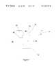
- FIG. 1shows a schematic cross section of a dielectric isolation layer to be planarized on a substrate, the layer having a height differential between portions.
- FIG. 2shows a schematic cross section of a dielectric isolation layer of FIG. 1 after leveling off of the height differential.
- FIG. 3shows a schematic cross section of a dielectric isolation layer of FIG. 2 after further reduction in height to reveal a stop layer.
- the inventionprovides slurry-less chemical-mechanical polishing processes which are effective in planarizing oxide materials even where the starting oxide material layer has significant topographical variation.
- the processes of the inventionare preferably characterized by the use of a fixed abrasive polishing element and by use of an aqueous liquid medium containing a polyelectrolyte for at least a portion of the polishing process involving reduction in the amount of any topographic variation (height differential) which may exist in the oxide material on the substrate.
- the inventionencompasses a method of polishing an oxide material layer on a substrate by slurry-less chemical-mechanical polishing, the method comprising:
- step d)maintaining the contact of step c) while providing movement between the substrate and polishing member, whereby the height differential becomes reduced.
- the inventionencompasses a method for removing exposed interlevel dielectric oxide from a substrate, the method comprising
- a substratehaving at least one feature selected from the group consisting of (i) a metal or conductive metal-containing structure contacting an exposed oxide layer, and (ii) a metal or conductive metal-containing structure having an exposed surface in an exposed oxide material layer,
- step d)maintaining the contact of step c) while providing movement between the substrate and polishing member, whereby oxide material is removed.
- step d)is preferably conducted until the oxide layer becomes reduced to a desired thickness and/or until a stop material (underlayer or metal feature) is exposed to a desired extent.
- the processes of the inventionmay be used to polish various oxide materials on various substrates, however the processes of the invention are especially useful in the context of oxide dielectric materials and substrates used in the production of integrated circuit devices and/or other microlithographically created articles.
- the materials to be polishedare preferably oxide dielectric materials to be configured or removed in the production of such devices or articles.
- the processes of the inventionare especially useful for the planarization or removal of siliceous oxide materials, more especially silicon dioxide materials.
- the processes of the inventionmay also be used with other siliceous materials such as doped silicon dioxide films (e.g., BPSG, BSG, etc.).
- the oxideis preferably a silicon oxide (e.g., SiO 2 ) and/or a silicate containing one or more elements selected from groups 3 A (e.g. boron) and 5 A (e.g. phosphorus or arsenic).
- the interlevel dielectricmay be adjacent to metal or metal-containing features formed from various materials such as copper, copper alloy, titanium, titanium nitride, tantalum, tantalum nitride, aluminum and/or aluminum alloy.
- the oxide material to be polishedmay be present without significant topography or may be relatively planar, however, the processes of the invention are especially useful where the initial dielectric oxide layer is non-planar at least in part because it is located over a surface already having at least one location of height differential.
- FIG. 1An example of such a structure is shown in FIG. 1 .
- the substrate 20has a first layer 30 (e.g., a silicon nitride stop layer) and a trench 45 (e.g., a trench to be filled with an oxide dielectric isolation material).
- the oxide material layer 40overfills trench 45 and oxide layer 40 has a depression 46 therein.
- the height differential His the distance between top surface 44 and depression surface 42 measured relative to a reference plane 10 .
- the processes of the inventionare especially useful for planarizing layers having height differentials of about 2000 ⁇ or more, especially about 4000 ⁇ or more. A typical height differential of interest will be on the order of about 4000 to 7000 ⁇ .
- Oxide material 40may be provided by various known techniques such as spin-on-glass (SOG) coating, chemical vapor deposition (CVD), physical vapor deposition, high density plasma or other technique. See for example, the various techniques discussed in “Fundamentals of Semiconductor Processing Technologies”, by Badih El-Kareh, Kluwer Academic Publishing, 1995 or other texts. Typically, deposition or formation of the dielectric oxide layer 40 over a surface having topography results in topographic variation in the oxide layer 40 .
- topographic variationmay occur in oxide layer 40 even where the structure underlayer 30 contains no topographic variation (not shown), for example, if the formation of oxide layer 40 is preferential over certain areas of layer 30 (e.g., due to variation of material composition in regions of layer 30 and/or due to the nature of the specific dielectric layer formation step itself). Topographic variation may also occur in oxide layer 40 where the structure underlayer 30 contains a topographic variation within a die and across the wafer. This variation may be attributed to variations in trench 45 depth and width. Layer 40 may contain one or more such regions having a height differential, e.g., where a plurality of trenches 45 are to be filled.
- the aqueous liquid mediumis characterized by the presence of a polyelectrolyte.
- the liquid mediumpreferably contains at least about 0.01 wt. % of polyelectrolyte, more preferably about 0.05-1.0 wt. %, most preferably about 0.1-0.5 wt. %.
- the polyelectrolyteis preferably selected from the group consisting of polyacrylic acid, polyethyleneimine, polymethylmethacrylate, polymethacrylic acid, polymaleic acid, or mixtures thereof. More preferably, the polyelectrolyte is polyacrylic acid.
- the polyelectrolytepreferably has a weight average molecular weight of about 500-20000, more preferably about 500-11000. Other polyelectrolytes, such as those described in U.S. Pat. No. 5,968,280, the disclosure of which is incorporated herein by reference, may also be used.
- the aqueous liquid mediumpreferably has a pH of about 4-13, more preferably about 9-13, most preferably about 10-12. Any suitable base may be used for establishing the pH level of the solution at an alkaline level, however, hydroxides such as ammonium hydroxide are preferred.
- the liquid mediummay contain other components known in the art, however the liquid medium preferably consists essentially of water, base and polyelectrolyte.
- step d)is continued at least until the step height differential is reduced to about 200 ⁇ or less for all portions of oxide layer 40 , at least until height differential H is substantially eliminated (e.g., as shown in FIG. 2 ).
- polishing step d)is carried out until a desired reduction in thickness is achieved in oxide layer 40 or more preferably until a stop layer 30 is exposed (e.g., as shown in FIG. 3 ).
- the process of the inventionenables the polishing from substantial step height differential through desired exposure of an underlayer (e.g., a stop layer) while achieving substantial planarization (i.e., without substantial topographic variation once the underlayer is desirably exposed).
- an underlayere.g., a stop layer
- the methods of the inventionare especially advantageous for obtaining planarization while stopping effectively on the underlayer.
- the underlayeris designed to act as a stop layer
- the inventionmay enable reduction in the thickness of that stop layer because of the increased ability of the methods of the invention to stop with high precision (i.e., without polishing through the stop layer).
- the inventionalso enables precise stopping of the polishing process without compromise of the polishing rate and without need for any special endpoint detection technique.
Landscapes
- Engineering & Computer Science (AREA)
- Physics & Mathematics (AREA)
- Condensed Matter Physics & Semiconductors (AREA)
- General Physics & Mathematics (AREA)
- Manufacturing & Machinery (AREA)
- Computer Hardware Design (AREA)
- Microelectronics & Electronic Packaging (AREA)
- Power Engineering (AREA)
- Mechanical Treatment Of Semiconductor (AREA)
- Internal Circuitry In Semiconductor Integrated Circuit Devices (AREA)
Abstract
Description
Claims (17)
Priority Applications (4)
| Application Number | Priority Date | Filing Date | Title |
|---|---|---|---|
| US09/469,922US6294470B1 (en) | 1999-12-22 | 1999-12-22 | Slurry-less chemical-mechanical polishing |
| US09/702,311US6569769B1 (en) | 1999-12-22 | 2000-10-31 | Slurry-less chemical-mechanical polishing |
| TW89125215ATW550139B (en) | 1999-12-22 | 2000-11-28 | Slurry-less chemical-mechanical polishing |
| KR10-2000-0075501AKR100412996B1 (en) | 1999-12-22 | 2000-12-12 | Slurry-less chemical-mechanical polishing |
Applications Claiming Priority (1)
| Application Number | Priority Date | Filing Date | Title |
|---|---|---|---|
| US09/469,922US6294470B1 (en) | 1999-12-22 | 1999-12-22 | Slurry-less chemical-mechanical polishing |
Related Child Applications (1)
| Application Number | Title | Priority Date | Filing Date |
|---|---|---|---|
| US09/702,311Continuation-In-PartUS6569769B1 (en) | 1999-12-22 | 2000-10-31 | Slurry-less chemical-mechanical polishing |
Publications (1)
| Publication Number | Publication Date |
|---|---|
| US6294470B1true US6294470B1 (en) | 2001-09-25 |
Family
ID=23865565
Family Applications (2)
| Application Number | Title | Priority Date | Filing Date |
|---|---|---|---|
| US09/469,922Expired - LifetimeUS6294470B1 (en) | 1999-12-22 | 1999-12-22 | Slurry-less chemical-mechanical polishing |
| US09/702,311Expired - LifetimeUS6569769B1 (en) | 1999-12-22 | 2000-10-31 | Slurry-less chemical-mechanical polishing |
Family Applications After (1)
| Application Number | Title | Priority Date | Filing Date |
|---|---|---|---|
| US09/702,311Expired - LifetimeUS6569769B1 (en) | 1999-12-22 | 2000-10-31 | Slurry-less chemical-mechanical polishing |
Country Status (2)
| Country | Link |
|---|---|
| US (2) | US6294470B1 (en) |
| KR (1) | KR100412996B1 (en) |
Cited By (12)
| Publication number | Priority date | Publication date | Assignee | Title |
|---|---|---|---|---|
| US6472292B2 (en)* | 2000-12-01 | 2002-10-29 | Sharp Kabushiki Kaisha | Process of manufacturing semiconductor device |
| US6485355B1 (en)* | 2001-06-22 | 2002-11-26 | International Business Machines Corporation | Method to increase removal rate of oxide using fixed-abrasive |
| US6569769B1 (en)* | 1999-12-22 | 2003-05-27 | International Business Machines Corporation | Slurry-less chemical-mechanical polishing |
| US20050079709A1 (en)* | 2003-10-13 | 2005-04-14 | International Business Machines Corporation | Planarization system and method using a carbonate containing fluid |
| US20060099814A1 (en)* | 2004-11-05 | 2006-05-11 | Cabot Microelectronics Corporation | Polishing composition and method for high silicon nitride to silicon oxide removal rate ratios |
| US20060108326A1 (en)* | 2004-11-05 | 2006-05-25 | Cabot Microelectronics | Polishing composition and method for high silicon nitride to silicon oxide removal rate ratios |
| US20060191872A1 (en)* | 2005-02-25 | 2006-08-31 | Webb Richard J | Method of polishing a wafer |
| US20070037491A1 (en)* | 2005-08-12 | 2007-02-15 | Yuzhuo Li | Chemically modified chemical mechanical polishing pad, process of making a modified chemical mechanical polishing pad and method of chemical mechanical polishing |
| US7291063B2 (en) | 2004-10-27 | 2007-11-06 | Ppg Industries Ohio, Inc. | Polyurethane urea polishing pad |
| US20080125018A1 (en)* | 2006-11-27 | 2008-05-29 | United Microelectronics Corp. | Solution for fixed abrasive chemical mechanical polishing process and fixed abrasive chemical mechanical polishing method |
| US20080287044A1 (en)* | 2007-05-14 | 2008-11-20 | Kuo-Wei Yang | Method of transferring a wafer |
| US20100243471A1 (en)* | 2007-10-31 | 2010-09-30 | 3M Innovative Properties Company | Composition, method and process for polishing a wafer |
Families Citing this family (4)
| Publication number | Priority date | Publication date | Assignee | Title |
|---|---|---|---|---|
| WO2003071593A1 (en)* | 2002-02-20 | 2003-08-28 | Ebara Corporation | Polishing method and polishing fluid |
| RU2354675C1 (en)* | 2005-09-30 | 2009-05-10 | Сэнт-Гобэн Керамикс Енд Пластикс, Инк. | Polishing suspension and method of ceramic part polishing |
| US8916448B2 (en)* | 2013-01-09 | 2014-12-23 | International Business Machines Corporation | Metal to metal bonding for stacked (3D) integrated circuits |
| US11037795B2 (en) | 2019-08-02 | 2021-06-15 | International Business Machines Corporation | Planarization of dielectric topography and stopping in dielectric |
Citations (19)
| Publication number | Priority date | Publication date | Assignee | Title |
|---|---|---|---|---|
| US5300463A (en)* | 1992-03-06 | 1994-04-05 | Micron Technology, Inc. | Method of selectively etching silicon dioxide dielectric layers on semiconductor wafers |
| US5352277A (en) | 1988-12-12 | 1994-10-04 | E. I. Du Pont De Nemours & Company | Final polishing composition |
| US5607718A (en) | 1993-03-26 | 1997-03-04 | Kabushiki Kaisha Toshiba | Polishing method and polishing apparatus |
| US5725417A (en) | 1996-11-05 | 1998-03-10 | Micron Technology, Inc. | Method and apparatus for conditioning polishing pads used in mechanical and chemical-mechanical planarization of substrates |
| US5733176A (en) | 1996-05-24 | 1998-03-31 | Micron Technology, Inc. | Polishing pad and method of use |
| US5782675A (en) | 1996-10-21 | 1998-07-21 | Micron Technology, Inc. | Apparatus and method for refurbishing fixed-abrasive polishing pads used in chemical-mechanical planarization of semiconductor wafers |
| US5855804A (en) | 1996-12-06 | 1999-01-05 | Micron Technology, Inc. | Method and apparatus for stopping mechanical and chemical-mechanical planarization of substrates at desired endpoints |
| US5876490A (en)* | 1996-12-09 | 1999-03-02 | International Business Machines Corporatin | Polish process and slurry for planarization |
| US5897424A (en) | 1995-07-10 | 1999-04-27 | The United States Of America As Represented By The Secretary Of Commerce | Renewable polishing lap |
| US5897426A (en) | 1998-04-24 | 1999-04-27 | Applied Materials, Inc. | Chemical mechanical polishing with multiple polishing pads |
| US5914275A (en) | 1992-05-26 | 1999-06-22 | Kabushiki Kaisha Toshiba | Polishing apparatus and method for planarizing layer on a semiconductor wafer |
| US5919082A (en) | 1997-08-22 | 1999-07-06 | Micron Technology, Inc. | Fixed abrasive polishing pad |
| US5958794A (en) | 1995-09-22 | 1999-09-28 | Minnesota Mining And Manufacturing Company | Method of modifying an exposed surface of a semiconductor wafer |
| US5968280A (en) | 1997-11-12 | 1999-10-19 | International Business Machines Corporation | Method for cleaning a surface |
| US5972124A (en) | 1998-08-31 | 1999-10-26 | Advanced Micro Devices, Inc. | Method for cleaning a surface of a dielectric material |
| US5972792A (en) | 1996-10-18 | 1999-10-26 | Micron Technology, Inc. | Method for chemical-mechanical planarization of a substrate on a fixed-abrasive polishing pad |
| US5981454A (en) | 1993-06-21 | 1999-11-09 | Ekc Technology, Inc. | Post clean treatment composition comprising an organic acid and hydroxylamine |
| US6132637A (en)* | 1996-09-27 | 2000-10-17 | Rodel Holdings, Inc. | Composition and method for polishing a composite of silica and silicon nitride |
| US6171352B1 (en)* | 1998-07-23 | 2001-01-09 | Eternal Chemical Co., Ltd. | Chemical mechanical abrasive composition for use in semiconductor processing |
Family Cites Families (7)
| Publication number | Priority date | Publication date | Assignee | Title |
|---|---|---|---|---|
| JPH02146732A (en)* | 1988-07-28 | 1990-06-05 | Fujitsu Ltd | Polishing liquid and polishing method |
| JPH0391920A (en)* | 1989-09-04 | 1991-04-17 | Canon Inc | electrolytic polishing liquid |
| CA2164127C (en)* | 1993-06-01 | 2004-06-22 | Michael E. Besse | Thickened hard surface cleaner |
| JP4204649B2 (en)* | 1996-02-05 | 2009-01-07 | 株式会社半導体エネルギー研究所 | Method for manufacturing semiconductor device |
| JPH10275789A (en)* | 1997-03-31 | 1998-10-13 | Sumitomo Chem Co Ltd | Abrasive and polishing method |
| US6017872A (en)* | 1998-06-08 | 2000-01-25 | Ecolab Inc. | Compositions and process for cleaning and finishing hard surfaces |
| US6294470B1 (en)* | 1999-12-22 | 2001-09-25 | International Business Machines Corporation | Slurry-less chemical-mechanical polishing |
- 1999
- 1999-12-22USUS09/469,922patent/US6294470B1/ennot_activeExpired - Lifetime
- 2000
- 2000-10-31USUS09/702,311patent/US6569769B1/ennot_activeExpired - Lifetime
- 2000-12-12KRKR10-2000-0075501Apatent/KR100412996B1/ennot_activeExpired - Fee Related
Patent Citations (19)
| Publication number | Priority date | Publication date | Assignee | Title |
|---|---|---|---|---|
| US5352277A (en) | 1988-12-12 | 1994-10-04 | E. I. Du Pont De Nemours & Company | Final polishing composition |
| US5300463A (en)* | 1992-03-06 | 1994-04-05 | Micron Technology, Inc. | Method of selectively etching silicon dioxide dielectric layers on semiconductor wafers |
| US5914275A (en) | 1992-05-26 | 1999-06-22 | Kabushiki Kaisha Toshiba | Polishing apparatus and method for planarizing layer on a semiconductor wafer |
| US5607718A (en) | 1993-03-26 | 1997-03-04 | Kabushiki Kaisha Toshiba | Polishing method and polishing apparatus |
| US5981454A (en) | 1993-06-21 | 1999-11-09 | Ekc Technology, Inc. | Post clean treatment composition comprising an organic acid and hydroxylamine |
| US5897424A (en) | 1995-07-10 | 1999-04-27 | The United States Of America As Represented By The Secretary Of Commerce | Renewable polishing lap |
| US5958794A (en) | 1995-09-22 | 1999-09-28 | Minnesota Mining And Manufacturing Company | Method of modifying an exposed surface of a semiconductor wafer |
| US5733176A (en) | 1996-05-24 | 1998-03-31 | Micron Technology, Inc. | Polishing pad and method of use |
| US6132637A (en)* | 1996-09-27 | 2000-10-17 | Rodel Holdings, Inc. | Composition and method for polishing a composite of silica and silicon nitride |
| US5972792A (en) | 1996-10-18 | 1999-10-26 | Micron Technology, Inc. | Method for chemical-mechanical planarization of a substrate on a fixed-abrasive polishing pad |
| US5782675A (en) | 1996-10-21 | 1998-07-21 | Micron Technology, Inc. | Apparatus and method for refurbishing fixed-abrasive polishing pads used in chemical-mechanical planarization of semiconductor wafers |
| US5725417A (en) | 1996-11-05 | 1998-03-10 | Micron Technology, Inc. | Method and apparatus for conditioning polishing pads used in mechanical and chemical-mechanical planarization of substrates |
| US5855804A (en) | 1996-12-06 | 1999-01-05 | Micron Technology, Inc. | Method and apparatus for stopping mechanical and chemical-mechanical planarization of substrates at desired endpoints |
| US5876490A (en)* | 1996-12-09 | 1999-03-02 | International Business Machines Corporatin | Polish process and slurry for planarization |
| US5919082A (en) | 1997-08-22 | 1999-07-06 | Micron Technology, Inc. | Fixed abrasive polishing pad |
| US5968280A (en) | 1997-11-12 | 1999-10-19 | International Business Machines Corporation | Method for cleaning a surface |
| US5897426A (en) | 1998-04-24 | 1999-04-27 | Applied Materials, Inc. | Chemical mechanical polishing with multiple polishing pads |
| US6171352B1 (en)* | 1998-07-23 | 2001-01-09 | Eternal Chemical Co., Ltd. | Chemical mechanical abrasive composition for use in semiconductor processing |
| US5972124A (en) | 1998-08-31 | 1999-10-26 | Advanced Micro Devices, Inc. | Method for cleaning a surface of a dielectric material |
Cited By (25)
| Publication number | Priority date | Publication date | Assignee | Title |
|---|---|---|---|---|
| US6569769B1 (en)* | 1999-12-22 | 2003-05-27 | International Business Machines Corporation | Slurry-less chemical-mechanical polishing |
| US6472292B2 (en)* | 2000-12-01 | 2002-10-29 | Sharp Kabushiki Kaisha | Process of manufacturing semiconductor device |
| US6485355B1 (en)* | 2001-06-22 | 2002-11-26 | International Business Machines Corporation | Method to increase removal rate of oxide using fixed-abrasive |
| DE10226235B4 (en)* | 2001-06-22 | 2010-02-18 | International Business Machines Corp. | A method of increasing the removal rate of oxide using a fixed abrasive |
| US7214623B2 (en) | 2003-10-13 | 2007-05-08 | International Business Machines Corporation | Planarization system and method using a carbonate containing fluid |
| US20050079709A1 (en)* | 2003-10-13 | 2005-04-14 | International Business Machines Corporation | Planarization system and method using a carbonate containing fluid |
| US7291063B2 (en) | 2004-10-27 | 2007-11-06 | Ppg Industries Ohio, Inc. | Polyurethane urea polishing pad |
| US7846842B2 (en) | 2004-11-05 | 2010-12-07 | Cabot Microelectronics Corporation | Polishing composition and method for high silicon nitride to silicon oxide removal rate ratios |
| US8138091B2 (en) | 2004-11-05 | 2012-03-20 | Cabot Microelectronics Corporation | Polishing composition and method for high silicon nitride to silicon oxide removal rate ratios |
| US7504044B2 (en) | 2004-11-05 | 2009-03-17 | Cabot Microelectronics Corporation | Polishing composition and method for high silicon nitride to silicon oxide removal rate ratios |
| US20060108326A1 (en)* | 2004-11-05 | 2006-05-25 | Cabot Microelectronics | Polishing composition and method for high silicon nitride to silicon oxide removal rate ratios |
| US20090215271A1 (en)* | 2004-11-05 | 2009-08-27 | Cabot Microelectronics Corporation | Polishing composition and method for high silicon nitride to silicon oxide removal rate ratios |
| US20060099814A1 (en)* | 2004-11-05 | 2006-05-11 | Cabot Microelectronics Corporation | Polishing composition and method for high silicon nitride to silicon oxide removal rate ratios |
| US7531105B2 (en) | 2004-11-05 | 2009-05-12 | Cabot Microelectronics Corporation | Polishing composition and method for high silicon nitride to silicon oxide removal rate ratios |
| US7449124B2 (en) | 2005-02-25 | 2008-11-11 | 3M Innovative Properties Company | Method of polishing a wafer |
| US20060191872A1 (en)* | 2005-02-25 | 2006-08-31 | Webb Richard J | Method of polishing a wafer |
| US20080034670A1 (en)* | 2005-08-12 | 2008-02-14 | Ppg Industries Ohio, Inc. | Chemically modified chemical mechanical polishing pad |
| US20070037491A1 (en)* | 2005-08-12 | 2007-02-15 | Yuzhuo Li | Chemically modified chemical mechanical polishing pad, process of making a modified chemical mechanical polishing pad and method of chemical mechanical polishing |
| US20080125018A1 (en)* | 2006-11-27 | 2008-05-29 | United Microelectronics Corp. | Solution for fixed abrasive chemical mechanical polishing process and fixed abrasive chemical mechanical polishing method |
| US20080287044A1 (en)* | 2007-05-14 | 2008-11-20 | Kuo-Wei Yang | Method of transferring a wafer |
| US7909677B2 (en) | 2007-05-14 | 2011-03-22 | United Microelectronics Corp. | Method of transferring a wafer |
| US20110076129A1 (en)* | 2007-05-14 | 2011-03-31 | Kuo-Wei Yang | Method of transferring a wafer |
| US8142258B2 (en) | 2007-05-14 | 2012-03-27 | United Microelectronics Corp. | Method of transferring a wafer |
| US20100243471A1 (en)* | 2007-10-31 | 2010-09-30 | 3M Innovative Properties Company | Composition, method and process for polishing a wafer |
| EP2217670A4 (en)* | 2007-10-31 | 2011-07-13 | 3M Innovative Properties Co | Composition, method and process for polishing a wafer |
Also Published As
| Publication number | Publication date |
|---|---|
| KR100412996B1 (en) | 2003-12-31 |
| US6569769B1 (en) | 2003-05-27 |
| KR20010062348A (en) | 2001-07-07 |
Similar Documents
| Publication | Publication Date | Title |
|---|---|---|
| US5169491A (en) | Method of etching SiO2 dielectric layers using chemical mechanical polishing techniques | |
| US6200897B1 (en) | Method for manufacturing even dielectric layer | |
| US6294470B1 (en) | Slurry-less chemical-mechanical polishing | |
| US6485355B1 (en) | Method to increase removal rate of oxide using fixed-abrasive | |
| US6191050B1 (en) | Interlayer dielectric with a composite dielectric stack | |
| US6632742B2 (en) | Method for avoiding defects produced in the CMP process | |
| US6235633B1 (en) | Method for making tungsten metal plugs in a polymer low-K intermetal dielectric layer using an improved two-step chemical/mechanical polishing process | |
| US7208404B2 (en) | Method to reduce Rs pattern dependence effect | |
| US6440840B1 (en) | Damascene process to eliminate copper defects during chemical-mechanical polishing (CMP) for making electrical interconnections on integrated circuits | |
| US6017803A (en) | Method to prevent dishing in chemical mechanical polishing | |
| JPH10173043A (en) | Method for forming contact plug of semiconductor device | |
| US6265315B1 (en) | Method for improving chemical/mechanical polish uniformity over rough topography for semiconductor integrated circuits | |
| US20020052117A1 (en) | Chemical-mechanical polishing method | |
| WO2000002235A1 (en) | Method of planarizing integrated circuits | |
| US20060183333A1 (en) | Methods of fabricating semiconductor device using sacrificial layer | |
| US6358850B1 (en) | Slurry-less chemical-mechanical polishing of oxide materials | |
| US7105925B2 (en) | Differential planarization | |
| US6653202B1 (en) | Method of shallow trench isolation (STI) formation using amorphous carbon | |
| US6566249B1 (en) | Planarized semiconductor interconnect topography and method for polishing a metal layer to form wide interconnect structures | |
| KR20070007696A (en) | Method for Manufacturing Semiconductor Device and Semiconductor Device | |
| US6274480B1 (en) | Method of Fabricating semiconductor device | |
| US6943114B2 (en) | Integration scheme for metal gap fill, with fixed abrasive CMP | |
| KR0177396B1 (en) | Surface planarization method of semiconductor device | |
| JP2000500920A (en) | Efficient and economical method of planarizing multilayer metallization structures in integrated circuits using CMP | |
| US6899597B2 (en) | Chemical mechanical polishing (CMP) process using fixed abrasive pads |
Legal Events
| Date | Code | Title | Description |
|---|---|---|---|
| AS | Assignment | Owner name:INFINEON TECHNOLOGIES NORTH AMERICA CORP., CALIFOR Free format text:ASSIGNMENT OF ASSIGNORS INTEREST;ASSIGNOR:SIMPSON, ALEXANDER;REEL/FRAME:010472/0668 Effective date:19991221 Owner name:INTERNATIONAL BUSINESS MACHINES CORPORATION, NEW Y Free format text:ASSIGNMENT OF ASSIGNORS INTEREST;ASSIGNOR:ECONOMIKOS, LAERTIS;REEL/FRAME:010472/0677 Effective date:19991221 | |
| STCF | Information on status: patent grant | Free format text:PATENTED CASE | |
| AS | Assignment | Owner name:INFINEON TECHNOLOGIES AG, GERMANY Free format text:ASSIGNMENT OF ASSIGNORS INTEREST;ASSIGNOR:INFINEON TECHNOLOGIES NORTH AMERICA CORP.;REEL/FRAME:013755/0792 Effective date:20030620 | |
| FEPP | Fee payment procedure | Free format text:PAYOR NUMBER ASSIGNED (ORIGINAL EVENT CODE: ASPN); ENTITY STATUS OF PATENT OWNER: LARGE ENTITY | |
| FPAY | Fee payment | Year of fee payment:4 | |
| FPAY | Fee payment | Year of fee payment:8 | |
| AS | Assignment | Owner name:QIMONDA AG, GERMANY Free format text:ASSIGNMENT OF ASSIGNORS INTEREST;ASSIGNOR:INFINEON TECHNOLOGIES AG;REEL/FRAME:023788/0535 Effective date:20060425 | |
| REMI | Maintenance fee reminder mailed | ||
| FPAY | Fee payment | Year of fee payment:12 | |
| SULP | Surcharge for late payment | Year of fee payment:11 | |
| AS | Assignment | Owner name:INFINEON TECHNOLOGIES AG, GERMANY Free format text:ASSIGNMENT OF ASSIGNORS INTEREST;ASSIGNOR:QIMONDA AG;REEL/FRAME:035623/0001 Effective date:20141009 |