US6294450B1 - Nanoscale patterning for the formation of extensive wires - Google Patents
Nanoscale patterning for the formation of extensive wiresDownload PDFInfo
- Publication number
- US6294450B1 US6294450B1US09/516,989US51698900AUS6294450B1US 6294450 B1US6294450 B1US 6294450B1US 51698900 AUS51698900 AUS 51698900AUS 6294450 B1US6294450 B1US 6294450B1
- Authority
- US
- United States
- Prior art keywords
- substrate
- layers
- platen
- alternating layers
- silicon
- Prior art date
- Legal status (The legal status is an assumption and is not a legal conclusion. Google has not performed a legal analysis and makes no representation as to the accuracy of the status listed.)
- Expired - Lifetime
Links
Images

Classifications
- H—ELECTRICITY
- H01—ELECTRIC ELEMENTS
- H01L—SEMICONDUCTOR DEVICES NOT COVERED BY CLASS H10
- H01L21/00—Processes or apparatus adapted for the manufacture or treatment of semiconductor or solid state devices or of parts thereof
- H01L21/02—Manufacture or treatment of semiconductor devices or of parts thereof
- H01L21/02104—Forming layers
- H01L21/02365—Forming inorganic semiconducting materials on a substrate
- H01L21/02518—Deposited layers
- H01L21/02587—Structure
- H01L21/0259—Microstructure
- H01L21/02603—Nanowires
- B—PERFORMING OPERATIONS; TRANSPORTING
- B82—NANOTECHNOLOGY
- B82Y—SPECIFIC USES OR APPLICATIONS OF NANOSTRUCTURES; MEASUREMENT OR ANALYSIS OF NANOSTRUCTURES; MANUFACTURE OR TREATMENT OF NANOSTRUCTURES
- B82Y10/00—Nanotechnology for information processing, storage or transmission, e.g. quantum computing or single electron logic
- B—PERFORMING OPERATIONS; TRANSPORTING
- B82—NANOTECHNOLOGY
- B82Y—SPECIFIC USES OR APPLICATIONS OF NANOSTRUCTURES; MEASUREMENT OR ANALYSIS OF NANOSTRUCTURES; MANUFACTURE OR TREATMENT OF NANOSTRUCTURES
- B82Y40/00—Manufacture or treatment of nanostructures
- G—PHYSICS
- G03—PHOTOGRAPHY; CINEMATOGRAPHY; ANALOGOUS TECHNIQUES USING WAVES OTHER THAN OPTICAL WAVES; ELECTROGRAPHY; HOLOGRAPHY
- G03F—PHOTOMECHANICAL PRODUCTION OF TEXTURED OR PATTERNED SURFACES, e.g. FOR PRINTING, FOR PROCESSING OF SEMICONDUCTOR DEVICES; MATERIALS THEREFOR; ORIGINALS THEREFOR; APPARATUS SPECIALLY ADAPTED THEREFOR
- G03F7/00—Photomechanical, e.g. photolithographic, production of textured or patterned surfaces, e.g. printing surfaces; Materials therefor, e.g. comprising photoresists; Apparatus specially adapted therefor
- G03F7/0002—Lithographic processes using patterning methods other than those involving the exposure to radiation, e.g. by stamping
- H—ELECTRICITY
- H01—ELECTRIC ELEMENTS
- H01L—SEMICONDUCTOR DEVICES NOT COVERED BY CLASS H10
- H01L21/00—Processes or apparatus adapted for the manufacture or treatment of semiconductor or solid state devices or of parts thereof
- H01L21/02—Manufacture or treatment of semiconductor devices or of parts thereof
- H01L21/02104—Forming layers
- H01L21/02365—Forming inorganic semiconducting materials on a substrate
- H01L21/02518—Deposited layers
- H01L21/02521—Materials
- H01L21/02524—Group 14 semiconducting materials
- H01L21/02532—Silicon, silicon germanium, germanium
- H—ELECTRICITY
- H01—ELECTRIC ELEMENTS
- H01L—SEMICONDUCTOR DEVICES NOT COVERED BY CLASS H10
- H01L21/00—Processes or apparatus adapted for the manufacture or treatment of semiconductor or solid state devices or of parts thereof
- H01L21/02—Manufacture or treatment of semiconductor devices or of parts thereof
- H01L21/02104—Forming layers
- H01L21/02365—Forming inorganic semiconducting materials on a substrate
- H01L21/02518—Deposited layers
- H01L21/02521—Materials
- H01L21/02538—Group 13/15 materials
- H01L21/02546—Arsenides
- H—ELECTRICITY
- H01—ELECTRIC ELEMENTS
- H01L—SEMICONDUCTOR DEVICES NOT COVERED BY CLASS H10
- H01L21/00—Processes or apparatus adapted for the manufacture or treatment of semiconductor or solid state devices or of parts thereof
- H01L21/02—Manufacture or treatment of semiconductor devices or of parts thereof
- H01L21/02104—Forming layers
- H01L21/02365—Forming inorganic semiconducting materials on a substrate
- H01L21/02612—Formation types
- H01L21/02617—Deposition types
- H01L21/0262—Reduction or decomposition of gaseous compounds, e.g. CVD
- H—ELECTRICITY
- H01—ELECTRIC ELEMENTS
- H01L—SEMICONDUCTOR DEVICES NOT COVERED BY CLASS H10
- H01L21/00—Processes or apparatus adapted for the manufacture or treatment of semiconductor or solid state devices or of parts thereof
- H01L21/02—Manufacture or treatment of semiconductor devices or of parts thereof
- H01L21/02104—Forming layers
- H01L21/02365—Forming inorganic semiconducting materials on a substrate
- H01L21/02612—Formation types
- H01L21/02617—Deposition types
- H01L21/02631—Physical deposition at reduced pressure, e.g. MBE, sputtering, evaporation
- H—ELECTRICITY
- H01—ELECTRIC ELEMENTS
- H01L—SEMICONDUCTOR DEVICES NOT COVERED BY CLASS H10
- H01L21/00—Processes or apparatus adapted for the manufacture or treatment of semiconductor or solid state devices or of parts thereof
- H01L21/02—Manufacture or treatment of semiconductor devices or of parts thereof
- H01L21/04—Manufacture or treatment of semiconductor devices or of parts thereof the devices having potential barriers, e.g. a PN junction, depletion layer or carrier concentration layer
- H01L21/18—Manufacture or treatment of semiconductor devices or of parts thereof the devices having potential barriers, e.g. a PN junction, depletion layer or carrier concentration layer the devices having semiconductor bodies comprising elements of Group IV of the Periodic Table or AIIIBV compounds with or without impurities, e.g. doping materials
- H01L21/30—Treatment of semiconductor bodies using processes or apparatus not provided for in groups H01L21/20 - H01L21/26
- H01L21/31—Treatment of semiconductor bodies using processes or apparatus not provided for in groups H01L21/20 - H01L21/26 to form insulating layers thereon, e.g. for masking or by using photolithographic techniques; After treatment of these layers; Selection of materials for these layers
- H01L21/3205—Deposition of non-insulating-, e.g. conductive- or resistive-, layers on insulating layers; After-treatment of these layers
- H01L21/321—After treatment
- H01L21/3213—Physical or chemical etching of the layers, e.g. to produce a patterned layer from a pre-deposited extensive layer
- H—ELECTRICITY
- H01—ELECTRIC ELEMENTS
- H01L—SEMICONDUCTOR DEVICES NOT COVERED BY CLASS H10
- H01L21/00—Processes or apparatus adapted for the manufacture or treatment of semiconductor or solid state devices or of parts thereof
- H01L21/70—Manufacture or treatment of devices consisting of a plurality of solid state components formed in or on a common substrate or of parts thereof; Manufacture of integrated circuit devices or of parts thereof
- H01L21/71—Manufacture of specific parts of devices defined in group H01L21/70
- H01L21/768—Applying interconnections to be used for carrying current between separate components within a device comprising conductors and dielectrics
- H01L21/76838—Applying interconnections to be used for carrying current between separate components within a device comprising conductors and dielectrics characterised by the formation and the after-treatment of the conductors
- Y—GENERAL TAGGING OF NEW TECHNOLOGICAL DEVELOPMENTS; GENERAL TAGGING OF CROSS-SECTIONAL TECHNOLOGIES SPANNING OVER SEVERAL SECTIONS OF THE IPC; TECHNICAL SUBJECTS COVERED BY FORMER USPC CROSS-REFERENCE ART COLLECTIONS [XRACs] AND DIGESTS
- Y10—TECHNICAL SUBJECTS COVERED BY FORMER USPC
- Y10S—TECHNICAL SUBJECTS COVERED BY FORMER USPC CROSS-REFERENCE ART COLLECTIONS [XRACs] AND DIGESTS
- Y10S977/00—Nanotechnology
- Y10S977/84—Manufacture, treatment, or detection of nanostructure
- Y10S977/887—Nanoimprint lithography, i.e. nanostamp
Definitions
- the present applicationis related to application Ser. No. 09/282,048, entitled “Chemically Synthesized and Assembled Electronic Devices”, filed on Mar. 29, 1999, which is directed to the formation of nanowires used for nanoscale computing and memory circuits.
- the present applicationis also related to applications Ser. No. 09/280,189, now issued as U.S. Pat. No. 6,128,214 for a “Molecular Wire Crossbar Memory;” Ser. No. 09/280,225, entitled “Molecular Wire Crossbar Interconnect (MWCI) for Signal Routing and Communications,” filed on Mar. 29, 1999; Ser. No. 09/282,045, entitled “Molecular Wire Crossbar Logic (MWCL),” filed on Mar. 29, 1999; and Ser. Nos.
- the present inventionis generally directed to nanoscale computing and memory circuits, and, more particularly, to the formation of nanowires for device applications.
- the self-assembled switching elementsmay be integrated on top of a Si integrated circuit so that they can be driven by conventional Si electronics in the underlying substrate.
- nanoscale interconnections or wireswith widths less than 10 ⁇ m and lengths exceeding 1 ⁇ m, are needed.
- the self-assembled wires connecting the conventional electronics to the self-assembled switching elementsshould be anchored at locations defined by the underlying circuitry and should be composed of materials compatible with Si integrated-circuit processing.
- a liquid alloy droplet containing the metal and Siis located at the tip of the wire and moves along with the growing end of the wire.
- the wiresmay either be formed in the gas phase or anchored at one end on a substrate; see, e.g., J. L.
- Titanium and TiSi 2are compatible with integrated-circuit technology and are frequently used in Si circuits to reduce resistance of silicon and polycrystalline-silicon conducting regions. Although Ti forms deep levels in Si, its solubility and diffusion coefficient in Si are low, and the deep levels are not at mid-gap. With suitable handling, Ti is generally accepted in integrated-circuit facilities.
- NanowiresLong, thin “nanowires” of silicon or other materials, such as carbon, can be formed by catalyst-enhanced reaction of gaseous precursors; see, e.g., the above-mentioned patent application Ser. No. 09/282,048.
- the catalystsare often metal-containing nanoparticles either on the surface of a substrate or suspended in the reactor ambient.
- the nanowiresmay be usefull in electronic or other devices as either connections to an electronic element such as a switch or as electronic elements themselves; see, e.g., the above-mentioned patent applications Ser. Nos. 09/280,225, 09/282,045, 09/699,080 and 09/699,269, and U.S. Pat. No. 6,128,214.
- nanowiresis important for device applications, such as logic circuits, crossbar memories, etc.
- Two lithographic fabrication approaches that have been used on larger scale devicesinclude electron beams and X-rays.
- the typical size of an electron beamis about 20 nm, and would require rastering the beam over a surface.
- the typical size of an X-ray beamis about 50 nm, and there are no lenses available to focus an X-ray beam.
- the use of X-raysrequires a synchrotron, and thus is very expensive. Neither approach permits generation and use of a beam on the order of 10 nm, which is required for nanowire fabrication.
- the present inventionsolves this problem, enabling the fabrication of nanowires with widths below 10 nm and with lengths extending into microscale dimensions, thereby avoiding the difficulties of rastering and the cost of a synchrotron, while permitting more accurate control of the placement of the nanowires.
- a method for forming a platen useful for forming nanoscale wires for device applicationscomprises:
- the pattern of the platenis then transferred into a substrate comprising a softer material to form a negative of the pattern, which is then used in further processing.
- a nano-imprinting devicecomprises a plurality of alternating layers of the two dissimilar materials, with the layers of one material etched relative the layers of the other material to form indentations of the one material.
- Each materialindependently has a thickness within a range of about 0.4 nm to several hundred nm. The device is then oriented such that the indentations are parallel to a surface to be imprinted and the pattern created by the indentations is imprinted into the surface.
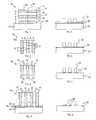
- FIG. 1is a cross-sectional view of a plurality of alternating layers of two materials, forming a stack on a major surface of a substrate and showing a cleaving surface;
- FIG. 2is a cross-sectional view of the stack rotated 90 degrees so as to place the cleaved surface facing downward;
- FIG. 3is a view similar to that of FIG. 2, but showing the effects of partially etching one of the materials relative to the other;
- FIG. 4is a view similar to that of FIG. 3, showing use of the etched stack as a molding master for nano-imprinting in a material that is softer than the etched material, depicting one embodiment of performing the nano-imprinting, using a thin (nanometer scale) metal layer on a substrate;
- FIG. 5is a view similar to that of FIG. 4, showing the negative formed in the softer material
- FIG. 6is a view similar to that of FIG. 5, following etching of the thin polymer residual layers to expose portions of the thin metal layer;
- FIG. 7is a view similar to that of FIG. 6, following etching of the exposed portions of the thin metal layer.
- FIG. 8is a view similar to that of FIG. 7, following removal of the remaining softer material to expose a plurality of parallel nano-wires.
- Nanoscale strips for device applicationsare fabricated by depositing composite thin films with different materials A and B, as illustrated in FIG. 1 .
- a plurality of alternating layers of A material 10 and B material 12are deposited on a major surface 14 a of a substrate 14 to form a stack 16 , also having a major surface 16 a , parallel to the major surface of the substrate.
- the material having the least lattice mis-match with the substrate 14is deposited in order to keep a smooth growth surface and flat, sharp interfaces between materials 10 and 12 .
- the layers 10 , 12are then cleaved along a line 18 normal to the major surface 16 a of the stack 16 to expose the cross-section, as shown in FIG. 2 .
- Cleavingis performed by any conventional technique useful in cleaving a plurality of alternating layers of dissimilar materials. Such techniques are well-known in the art for the materials used for layers A and B, which are discussed below.
- the material B, layer 12is then etched to a certain depth, as shown in FIG. 3, and as more fully described below, thereby providing the surface with extensive strips of indentations, shown by arrows 20 .
- the second, fourth, sixth, etc. layers from the substrateare etched.
- the indentations 20can be used as a platen 16 ′ to mold a master in layer 22 for nano-imprinting technology, as illustrated in FIG. 4 .
- the layer 22may comprise a thermoplastic polymer, for example, formed on a substrate 24 , which may comprise a semiconductor or metal material.
- the pattern of the polymer nanowires formed in layer 22shown in FIG. 5, can then be transferred to metal and/or semiconductor nanowires by using conventional lithographic and ink printing processes; see, e.g., X. Sun et al, “Multilayer resist methods for nanoimprint lithography on nonflat surfaces”, Journal of Vacuum Science and Technology , Vol. B16, No. 6, pp. 3922-3925 (1998).
- etching rate of one material relative to the otheris immaterial, except that the B material must etch at a faster rate than the A material.
- a differential etching rate of more than five times fasteris employed in order to minimize the amount of etching of the A material.
- the concentration of siliconranges from about 70 to 90 atomic percent (at %), and the balance (30 to 10 at %) is germanium.
- the concentration of Alranges from a few percent to 100 at % (AlAs).
- the alloyis represented as Al x Ga 1 ⁇ x As, where x ranges from a few at % to 100 at %.
- the two layers 10 , 12each independently have a thickness range of about 0.4 nm to several hundred nm, and are conveniently deposited by chemical vapor deposition (CVD), using organo-silanes and organo-germanes (for the Si/Si—Ge system) or appropriate precursors for AlGaAs and GaAs, as is well-known.
- Molecular beam epitaxy (MBE)may be alternatively employed in the depositions of the two materials, using well-known procedures. The particular method of forming the A and B layers does not form a part of the present invention.
- the two materials A and Bare conveniently deposited on a semiconductor substrate, silicon in the case of the Si/Si—Ge system or gallium arsenide in the case of the AlGaAs/GaAs system (see Table I).
- a semiconductor substratesilicon in the case of the Si/Si—Ge system or gallium arsenide in the case of the AlGaAs/GaAs system (see Table I).
- lattice mis-matchis always a consideration, and selection of substrate and materials A and B will be dictated by minimizing the strain resulting from lattice mis-match. Such a determination is easily within the ability of the person skilled in this art, and therefore does not constitute undue experimentation.
- Layers of the A and B materialsare deposited on the substrate in alternating fashion, each layer having a thickness within the range listed above.
- the number of A and B layersdepends on the requirement for the devices - a large number of devices requires many wires in parallel, while a smaller number of devices requires fewer wires in parallel.
- the number of A and B layersis within the range of a few layers of each material to several thousand layers of each material.
- the A and B layerscan be formed with varying thicknesses, for making nonperiodic arrays of wires.
- wires and spacings of different widths and a periodic structuresmay be formed in accordance with the teachings of the present invention.
- Such a periodic arraysare useful, for example, for making blocks of crossbars with larger wires for multiplexing.
- the etching of the two materials A and Bis advantageously performed by chemical etching, and known etchants are employed that have the requisite etch rate differential between the two materials used.
- the depth of etching (indentations 20 )may range from several nm to several hundred nm, and depends on the requirement of the height of the nanowires ultimately formed by nano-imprinting.
- Nano-imprintinginvolves pressing a platen 16 ′ into a softer material 22 , such as a thermoplastic polymer, thereby transferring a negative of the pattern formed by the indentations 18 into the softer material.
- a softer material 22such as a thermoplastic polymer
- suitable thermoplastic materialsinclude polymethyl methacrylate (PMMA) and methyl methacrylate (MMA).
- PMMApolymethyl methacrylate
- MMAmethyl methacrylate
- MMAmethyl methacrylate
- other thermoplastic materials and, indeed, materials other than thermoplastic materialsmay be employed in the practice of the present invention, so long as the material 22 is softer than that of the platen 16 ′.
- the resulting imprinted pattern, imprinted by the platen 16 ′ into the softer material 22is then transferred into a substrate, e.g., semiconductor or metal, as a positive image of the platen.
- a substratee.g., semiconductor or metal
- the transferred patterncan then be used for further processing in the formation of nanoscale devices.
- FIGS. 4-8depict one such method, but it will be understood that the present invention is not so limited.
- a thin metal layer 26is first formed on the substrate, followed by formation of the soft material thereon.
- the thickness of the thin metal layer 26is in the nanoscale region, that is, on the order of several nanometers to hundreds of nanometers.
- the thinner portions of the soft material 22are removed, such as by etching with an etchant that removes the soft material but does not etch the metal layer 26 , thereby exposing portions of the thin metal layer. This step is depicted in FIG. 6 .
- the exposed portions of the metal layer 26are removed, leaving behind those portions 26 ′ of the metal layer covered by the soft material 22 , as shown in FIG. 7 .
- the remaining soft material 22is then removed, leaving a plurality of parallel metal lines 26 ′ on the surface of the substrate 24 .
- the metal lines 26 ′being of nanoscale thickness, are then further processed to form nanoscale devices, as taught elsewhere.
- the foregoing methodis directed to the formation of a plurality of alternating layers 10 , 12 , used to form a platen 16 ′.
- the particular method of forming the plurality of alternating layers 10 , 12is immaterial to the method of the present invention, although two processes, CVD and MBE, are mentioned above.
- An alternate technique, called “spontaneous ordering”is an example of another process useful in the practice of the present invention. Spontaneous ordering is discussed, for example, by Z. Lilienthal-Weber et al, “Spontaneous Ordering in Bulk GaN:Mg Samples”, Physical Review Letters , Vol. 83, No. 12, pp. 2370-2373 (Sept. 20, 1999).
- one material with a homogeneous structure (or concentration)can decompose and form a superlattice with alternating layers of two or more dissimilar materials with different structures (or concentrations).
- the magnesium atoms in GaNtend to concentrate and form regular periodic thin Mg-rich layers buried in GaN.
- These periodic superlattices formed by spontaneous orderingcan also be to form the platen 16 ′.
- the method of nanoscale patterning for the formation of extensive nanowiresis expected to find use in nanoscale computing and memory circuits.
Landscapes
- Engineering & Computer Science (AREA)
- Physics & Mathematics (AREA)
- General Physics & Mathematics (AREA)
- Chemical & Material Sciences (AREA)
- Condensed Matter Physics & Semiconductors (AREA)
- Manufacturing & Machinery (AREA)
- Nanotechnology (AREA)
- Power Engineering (AREA)
- Microelectronics & Electronic Packaging (AREA)
- Computer Hardware Design (AREA)
- Crystallography & Structural Chemistry (AREA)
- Mathematical Physics (AREA)
- Theoretical Computer Science (AREA)
- Exposure Of Semiconductors, Excluding Electron Or Ion Beam Exposure (AREA)
- Semiconductor Memories (AREA)
- Internal Circuitry In Semiconductor Integrated Circuit Devices (AREA)
- Shaping Of Tube Ends By Bending Or Straightening (AREA)
- Drying Of Semiconductors (AREA)
Abstract
Description
| TABLE I |
| Examples of A and B Materials. |
| A MATERIAL | B MATERIAL | SUBSTRATE |
| Si | Si—Ge alloy | Si |
| AlGaAs | GaAs | GaAs |
Claims (16)
Priority Applications (6)
| Application Number | Priority Date | Filing Date | Title |
|---|---|---|---|
| US09/516,989US6294450B1 (en) | 2000-03-01 | 2000-03-01 | Nanoscale patterning for the formation of extensive wires |
| JP2001564392AJP2004500250A (en) | 2000-03-01 | 2001-02-22 | Nanoscale patterning to form a wide range of wires |
| KR1020027011346AKR100744884B1 (en) | 2000-03-01 | 2001-02-22 | Nanoscale patterning for the formation of long wires |
| EP01912948AEP1301944A2 (en) | 2000-03-01 | 2001-02-22 | Nanoscale patterning for the formation of extensive wires |
| PCT/US2001/005734WO2001065600A2 (en) | 2000-03-01 | 2001-02-22 | Nanoscale patterning for the formation of extensive wires |
| US09/886,355US6407443B2 (en) | 2000-03-01 | 2001-06-20 | Nanoscale patterning for the formation of extensive wires |
Applications Claiming Priority (1)
| Application Number | Priority Date | Filing Date | Title |
|---|---|---|---|
| US09/516,989US6294450B1 (en) | 2000-03-01 | 2000-03-01 | Nanoscale patterning for the formation of extensive wires |
Related Child Applications (1)
| Application Number | Title | Priority Date | Filing Date |
|---|---|---|---|
| US09/886,355DivisionUS6407443B2 (en) | 2000-03-01 | 2001-06-20 | Nanoscale patterning for the formation of extensive wires |
Publications (1)
| Publication Number | Publication Date |
|---|---|
| US6294450B1true US6294450B1 (en) | 2001-09-25 |
Family
ID=24057911
Family Applications (2)
| Application Number | Title | Priority Date | Filing Date |
|---|---|---|---|
| US09/516,989Expired - LifetimeUS6294450B1 (en) | 2000-03-01 | 2000-03-01 | Nanoscale patterning for the formation of extensive wires |
| US09/886,355Expired - LifetimeUS6407443B2 (en) | 2000-03-01 | 2001-06-20 | Nanoscale patterning for the formation of extensive wires |
Family Applications After (1)
| Application Number | Title | Priority Date | Filing Date |
|---|---|---|---|
| US09/886,355Expired - LifetimeUS6407443B2 (en) | 2000-03-01 | 2001-06-20 | Nanoscale patterning for the formation of extensive wires |
Country Status (5)
| Country | Link |
|---|---|
| US (2) | US6294450B1 (en) |
| EP (1) | EP1301944A2 (en) |
| JP (1) | JP2004500250A (en) |
| KR (1) | KR100744884B1 (en) |
| WO (1) | WO2001065600A2 (en) |
Cited By (98)
| Publication number | Priority date | Publication date | Assignee | Title |
|---|---|---|---|---|
| US20030071246A1 (en)* | 2001-01-23 | 2003-04-17 | Grigorov Leonid N. | Quantum devices based on crystallized electron pairs and methods for their manufacture and use |
| US20030100189A1 (en)* | 2001-11-28 | 2003-05-29 | Chun-Tao Lee | Method for increasing the capacity of an integrated circuit device |
| US6596187B2 (en)* | 2001-08-29 | 2003-07-22 | Motorola, Inc. | Method of forming a nano-supported sponge catalyst on a substrate for nanotube growth |
| US20030177450A1 (en)* | 2002-03-12 | 2003-09-18 | Alex Nugent | Physical neural network design incorporating nanotechnology |
| US20030194875A1 (en)* | 2002-04-13 | 2003-10-16 | The Board Of Trustees Of The University Of Illinois | Method for large-scale fabrication of atomic-scale structures on material surfaces using surface vacancies |
| US20040005723A1 (en)* | 2002-04-02 | 2004-01-08 | Nanosys, Inc. | Methods of making, positioning and orienting nanostructures, nanostructure arrays and nanostructure devices |
| US20040028812A1 (en)* | 2002-08-08 | 2004-02-12 | Jurina Wessels | Method for preparing a nanowire crossbar structure and use of a structure prepared by this method |
| US20040041617A1 (en)* | 2002-08-30 | 2004-03-04 | Snider Gregory S. | Configurable molecular switch array |
| US20040061151A1 (en)* | 2002-09-27 | 2004-04-01 | James Stasiak | Nanometer-scale semiconductor devices and method of making |
| WO2004012234A3 (en)* | 2002-07-30 | 2004-04-01 | Univ California | Superlattice nanopatterning of wires and complex patterns |
| US20040079278A1 (en)* | 2002-10-28 | 2004-04-29 | Kamins Theodore I. | Method of forming three-dimensional nanocrystal array |
| US20040110856A1 (en)* | 2002-12-04 | 2004-06-10 | Young Jung Gun | Polymer solution for nanoimprint lithography to reduce imprint temperature and pressure |
| US6748865B2 (en)* | 2001-11-22 | 2004-06-15 | Kabushiki Kaisha Toshiba | Nano-imprinting method, magnetic printing method and recording medium |
| US20040153426A1 (en)* | 2002-03-12 | 2004-08-05 | Alex Nugent | Physical neural network liquid state machine utilizing nanotechnology |
| US6773616B1 (en)* | 2001-11-13 | 2004-08-10 | Hewlett-Packard Development Company, L.P. | Formation of nanoscale wires |
| US20040162796A1 (en)* | 2002-03-12 | 2004-08-19 | Alex Nugent | Application of Hebbian and anti-Hebbian learning to nanotechnology-based physical neural networks |
| EP1333324A3 (en)* | 2002-01-31 | 2004-09-29 | Hewlett-Packard Company | Nano-size imprinting stamp |
| US20040214447A1 (en)* | 2003-04-24 | 2004-10-28 | James Stasiak | Sensor produced using imprint lithography |
| US20050014385A1 (en)* | 2003-07-15 | 2005-01-20 | Ghozeil Adam L. | Array of nanoscopic mosfet transistors and fabrication methods |
| US20050015351A1 (en)* | 2003-07-18 | 2005-01-20 | Alex Nugent | Nanotechnology neural network methods and systems |
| US20050037916A1 (en)* | 2003-08-15 | 2005-02-17 | Yong Chen | Imprinting nanoscale patterns for catalysis and fuel cells |
| US20050042465A1 (en)* | 2003-08-22 | 2005-02-24 | Clemson Unviersity | Thermal CVD synthesis of nanostructures |
| US20050074911A1 (en)* | 2003-10-07 | 2005-04-07 | Pavel Kornilovich | Fabricationof nano-object array |
| US20050072967A1 (en)* | 2003-10-07 | 2005-04-07 | Pavel Kornilovich | Fabrication of nanowires |
| US20050123674A1 (en)* | 2003-05-05 | 2005-06-09 | James Stasiak | Imprint lithography for superconductor devices |
| US20050161431A1 (en)* | 2004-01-27 | 2005-07-28 | Heon Lee | Silicon carbide imprint stamp |
| US6936496B2 (en) | 2002-12-20 | 2005-08-30 | Hewlett-Packard Development Company, L.P. | Nanowire filament |
| US20050221235A1 (en)* | 2004-04-02 | 2005-10-06 | Pavel Kornilovich | Fabrication and use of superlattice |
| US20050245057A1 (en)* | 2004-04-30 | 2005-11-03 | Xiaofeng Yang | Misalignment-tolerant methods for fabricating multiplexing/demultiplexing architectures |
| US20050242404A1 (en)* | 2004-04-30 | 2005-11-03 | Xiaofeng Yang | Misalignment-tolerant multiplexing/demultiplexing architectures |
| US20050241959A1 (en)* | 2004-04-30 | 2005-11-03 | Kenneth Ward | Chemical-sensing devices |
| US20050245014A1 (en)* | 2004-04-30 | 2005-11-03 | Xiaofeng Yang | Field-effect-transistor multiplexing/demultiplexing architectures and methods of forming the same |
| US20050248003A1 (en)* | 2004-02-17 | 2005-11-10 | Leonid Tsybeskov | One dimensional nanostructures for vertical heterointegration on a silicon platform and method for making same |
| US20050281075A1 (en)* | 2004-06-17 | 2005-12-22 | Zhizhang Chen | Semiconductor storage device |
| US20060012079A1 (en)* | 2004-07-16 | 2006-01-19 | Gun-Young Jung | Formation of a self-assembled release monolayer in the vapor phase |
| US20060021967A1 (en)* | 2004-01-27 | 2006-02-02 | Heon Lee | Imprint stamp |
| US20060024814A1 (en)* | 2004-07-29 | 2006-02-02 | Peters Kevin F | Aptamer-functionalized electrochemical sensors and methods of fabricating and using the same |
| US20060043626A1 (en)* | 2004-09-01 | 2006-03-02 | Wei Wu | Imprint lithography apparatus and method employing an effective pressure |
| US20060046069A1 (en)* | 2004-08-30 | 2006-03-02 | Jung Gun Y | Increasing adhesion in an imprinting procedure |
| US20060063368A1 (en)* | 2004-09-17 | 2006-03-23 | Shashank Sharma | Reduction of a feature dimension in a nano-scale device |
| US20060157684A1 (en)* | 2004-12-15 | 2006-07-20 | The Regents Of The University Of California | Thin film multilayer with nanolayers addressable from the macroscale |
| US20060164634A1 (en)* | 2005-01-27 | 2006-07-27 | Kamins Theodore I | Nano-enhanced Raman spectroscopy-active nanostructures including elongated components and methods of making the same |
| US20060184466A1 (en)* | 2005-01-31 | 2006-08-17 | Alex Nugent | Fractal memory and computational methods and systems based on nanotechnology |
| US20060194420A1 (en)* | 2005-02-28 | 2006-08-31 | Pavel Kornilovich | Multilayer film |
| US20060198919A1 (en)* | 2005-03-01 | 2006-09-07 | Tong William M | Method of fabricating a mold for imprinting a structure |
| US7141866B1 (en) | 2004-04-16 | 2006-11-28 | Hewlett-Packard Development Company, L.P. | Apparatus for imprinting lithography and fabrication thereof |
| US20070005532A1 (en)* | 2005-05-23 | 2007-01-04 | Alex Nugent | Plasticity-induced self organizing nanotechnology for the extraction of independent components from a data stream |
| US20070034909A1 (en)* | 2003-09-22 | 2007-02-15 | James Stasiak | Nanometer-scale semiconductor devices and method of making |
| US20070105353A1 (en)* | 2005-11-09 | 2007-05-10 | Tong William M | Metallic quantum dots fabricated by a superlattice structure |
| US20070164476A1 (en)* | 2004-09-01 | 2007-07-19 | Wei Wu | Contact lithography apparatus and method employing substrate deformation |
| US20070177139A1 (en)* | 2006-01-27 | 2007-08-02 | Kamins Theodore I | Nanowire heterostructures and methods of forming the same |
| US20070176643A1 (en)* | 2005-06-17 | 2007-08-02 | Alex Nugent | Universal logic gate utilizing nanotechnology |
| US7256435B1 (en) | 2003-06-02 | 2007-08-14 | Hewlett-Packard Development Company, L.P. | Multilevel imprint lithography |
| US20070215480A1 (en)* | 2006-03-16 | 2007-09-20 | Fang Nicholas X | Pattern transfer by solid state electrochemical stamping |
| US20070275193A1 (en)* | 2004-02-13 | 2007-11-29 | Desimone Joseph M | Functional Materials and Novel Methods for the Fabrication of Microfluidic Devices |
| US20080084006A1 (en)* | 2006-10-10 | 2008-04-10 | Jun Gao | Hydraulic-facilitated contact lithography apparatus, system and method |
| US20080090155A1 (en)* | 2006-10-12 | 2008-04-17 | Stewart Duncan R | Deformation-based contact lithography systems, apparatus and methods |
| US20080090160A1 (en)* | 2006-10-13 | 2008-04-17 | Jason Blackstock | Alignment for contact lithography |
| US20080089470A1 (en)* | 2006-10-13 | 2008-04-17 | Walmsley Robert G | Alignment for contact lithography |
| US20080087636A1 (en)* | 2006-10-12 | 2008-04-17 | Wei Wu | Contact lithography apparatus and method |
| US7398259B2 (en) | 2002-03-12 | 2008-07-08 | Knowmtech, Llc | Training of a physical neural network |
| CN100409450C (en)* | 2002-03-28 | 2008-08-06 | 皇家飞利浦电子股份有限公司 | Nanowires and Electronic Devices |
| WO2008138361A1 (en)* | 2007-05-09 | 2008-11-20 | Technische Universität München | Mold for generating nanostructures, and mold holder unit |
| US20090027603A1 (en)* | 2005-02-03 | 2009-01-29 | Samulski Edward T | Low Surface Energy Polymeric Material for Use in Liquid Crystal Displays |
| US20090028910A1 (en)* | 2003-12-19 | 2009-01-29 | University Of North Carolina At Chapel Hill | Methods for Fabrication Isolated Micro-and Nano-Structures Using Soft or Imprint Lithography |
| US20090043722A1 (en)* | 2003-03-27 | 2009-02-12 | Alex Nugent | Adaptive neural network utilizing nanotechnology-based components |
| US20090050487A1 (en)* | 2006-03-16 | 2009-02-26 | Fang Nicholas X | Direct Nanoscale Patterning of Metals Using Polymer Electrolytes |
| DE112007001740T5 (en) | 2006-07-24 | 2009-06-18 | Hewlett-Packard Development Company, L.P., Houston | Alignment for contact lithography |
| US20090165320A1 (en)* | 2003-09-23 | 2009-07-02 | Desimone Joseph M | Photocurable perfluoropolyethers for use as novel materials in microfluidic devices |
| US20090228415A1 (en)* | 2002-06-05 | 2009-09-10 | Alex Nugent | Multilayer training in a physical neural network formed utilizing nanotechnology |
| US20090228416A1 (en)* | 2002-08-22 | 2009-09-10 | Alex Nugent | High density synapse chip using nanoparticles |
| DE112007002430T5 (en) | 2006-10-13 | 2009-09-24 | Hewlett-Packard Development Company, L.P., Houston | Contact lithography apparatus, system and method |
| US7599895B2 (en) | 2005-07-07 | 2009-10-06 | Knowm Tech, Llc | Methodology for the configuration and repair of unreliable switching elements |
| US20090296058A1 (en)* | 2008-06-02 | 2009-12-03 | Asml Netherlands B.V. | Lithographic apparatus and device manufacturing method |
| US20090304992A1 (en)* | 2005-08-08 | 2009-12-10 | Desimone Joseph M | Micro and Nano-Structure Metrology |
| US20100021577A1 (en)* | 2005-08-12 | 2010-01-28 | Stewart Duncan R | Contact lithography apparatus, system and method |
| US20100151031A1 (en)* | 2007-03-23 | 2010-06-17 | Desimone Joseph M | Discrete size and shape specific organic nanoparticles designed to elicit an immune response |
| US20100227125A1 (en)* | 2009-03-03 | 2010-09-09 | Commissariat A L'energie Atomique | Method to fabricate a mould for lithography by nano-imprinting |
| US20100227018A1 (en)* | 2009-03-03 | 2010-09-09 | Commissariat A L' Energie Atomique | Method to fabricate a mould for lithography by nano-imprinting |
| US20100243990A1 (en)* | 2000-12-11 | 2010-09-30 | President And Fellows Of Harvard College | Nanosensors |
| US7915151B2 (en) | 2000-08-22 | 2011-03-29 | President And Fellows Of Harvard College | Doped elongated semiconductors, growing such semiconductors, devices including such semiconductors and fabricating such devices |
| US7930257B2 (en) | 2007-01-05 | 2011-04-19 | Knowm Tech, Llc | Hierarchical temporal memory utilizing nanotechnology |
| US8158728B2 (en) | 2004-02-13 | 2012-04-17 | The University Of North Carolina At Chapel Hill | Methods and materials for fabricating microfluidic devices |
| US20130260058A1 (en)* | 2002-12-14 | 2013-10-03 | Plastic Logic Limited | Electronic devices |
| US8575663B2 (en) | 2006-11-22 | 2013-11-05 | President And Fellows Of Harvard College | High-sensitivity nanoscale wire sensors |
| US8623288B1 (en) | 2009-06-29 | 2014-01-07 | Nanosys, Inc. | Apparatus and methods for high density nanowire growth |
| US20140024202A1 (en)* | 2007-05-07 | 2014-01-23 | Wisconsin Alumni Research Foundation | Semiconductor nanowire thermoelectric materials and devices, and processes for producing same |
| US9040090B2 (en) | 2003-12-19 | 2015-05-26 | The University Of North Carolina At Chapel Hill | Isolated and fixed micro and nano structures and methods thereof |
| US9269043B2 (en) | 2002-03-12 | 2016-02-23 | Knowm Tech, Llc | Memristive neural processor utilizing anti-hebbian and hebbian technology |
| US9297796B2 (en) | 2009-09-24 | 2016-03-29 | President And Fellows Of Harvard College | Bent nanowires and related probing of species |
| US9576595B1 (en) | 2014-11-19 | 2017-02-21 | Seagate Technology Llc | Transfer printing an epitaxial layer to a read/write head to form an integral laser |
| US9607638B1 (en) | 2014-11-19 | 2017-03-28 | Seagate Technology Llc | Recording head with an on-wafer integrated laser |
| US9903862B2 (en) | 2006-06-12 | 2018-02-27 | President And Fellows Of Harvard College | Nanosensors and related technologies |
| US10069029B1 (en) | 2014-11-19 | 2018-09-04 | Seagate Technology Llc | Transfer-printed photonics |
| US10783917B1 (en) | 2016-11-29 | 2020-09-22 | Seagate Technology Llc | Recording head with transfer-printed laser diode unit formed of non-self-supporting layers |
| US10984821B1 (en) | 2014-11-19 | 2021-04-20 | Seagate Technology Llc | Transfer-printed near-field transducer and heat sink |
| US11069376B1 (en) | 2018-02-21 | 2021-07-20 | Seagate Technology Llc | Waveguide with optical isolator for heat-assisted magnetic recording |
| US11423928B1 (en) | 2018-01-19 | 2022-08-23 | Seagate Technology Llc | Processing for forming single-grain near-field transducer |
Families Citing this family (45)
| Publication number | Priority date | Publication date | Assignee | Title |
|---|---|---|---|---|
| US6732562B2 (en)* | 2000-05-09 | 2004-05-11 | University Of Central Florida | Apparatus and method for drawing continuous fiber |
| US6643165B2 (en) | 2001-07-25 | 2003-11-04 | Nantero, Inc. | Electromechanical memory having cell selection circuitry constructed with nanotube technology |
| US6706402B2 (en) | 2001-07-25 | 2004-03-16 | Nantero, Inc. | Nanotube films and articles |
| US7259410B2 (en) | 2001-07-25 | 2007-08-21 | Nantero, Inc. | Devices having horizontally-disposed nanofabric articles and methods of making the same |
| US6911682B2 (en) | 2001-12-28 | 2005-06-28 | Nantero, Inc. | Electromechanical three-trace junction devices |
| US6919592B2 (en) | 2001-07-25 | 2005-07-19 | Nantero, Inc. | Electromechanical memory array using nanotube ribbons and method for making same |
| US6924538B2 (en) | 2001-07-25 | 2005-08-02 | Nantero, Inc. | Devices having vertically-disposed nanofabric articles and methods of making the same |
| US6574130B2 (en)* | 2001-07-25 | 2003-06-03 | Nantero, Inc. | Hybrid circuit having nanotube electromechanical memory |
| US6835591B2 (en) | 2001-07-25 | 2004-12-28 | Nantero, Inc. | Methods of nanotube films and articles |
| US7176505B2 (en) | 2001-12-28 | 2007-02-13 | Nantero, Inc. | Electromechanical three-trace junction devices |
| US6784028B2 (en) | 2001-12-28 | 2004-08-31 | Nantero, Inc. | Methods of making electromechanical three-trace junction devices |
| US20040039717A1 (en)* | 2002-08-22 | 2004-02-26 | Alex Nugent | High-density synapse chip using nanoparticles |
| US7335395B2 (en) | 2002-04-23 | 2008-02-26 | Nantero, Inc. | Methods of using pre-formed nanotubes to make carbon nanotube films, layers, fabrics, ribbons, elements and articles |
| KR100925144B1 (en)* | 2002-12-18 | 2009-11-05 | 인터내셔널 비지네스 머신즈 코포레이션 | Method of self-assembling electronic circuitry and circuits formed thereby |
| WO2004059730A1 (en)* | 2002-12-18 | 2004-07-15 | International Business Machines Corporation | Method of self-assembling electronic circuitry and circuits formed thereby |
| JP4247379B2 (en)* | 2003-02-14 | 2009-04-02 | 国立大学法人大阪大学 | Method for producing porous body |
| US7416993B2 (en)* | 2003-09-08 | 2008-08-26 | Nantero, Inc. | Patterned nanowire articles on a substrate and methods of making the same |
| US7344753B2 (en)* | 2003-09-19 | 2008-03-18 | The Board Of Trustees Of The University Of Illinois | Nanostructures including a metal |
| US8030833B2 (en)* | 2003-09-19 | 2011-10-04 | The Board Of Trustees Of The University Of Illinois | Electron emission device incorporating free standing monocrystalline nanowires |
| US8617965B1 (en) | 2004-02-19 | 2013-12-31 | Partial Assignment to University of Central Florida | Apparatus and method of forming high crystalline quality layer |
| US7618880B1 (en)* | 2004-02-19 | 2009-11-17 | Quick Nathaniel R | Apparatus and method for transformation of substrate |
| US7268063B1 (en)* | 2004-06-01 | 2007-09-11 | University Of Central Florida | Process for fabricating semiconductor component |
| US7419887B1 (en)* | 2004-07-26 | 2008-09-02 | Quick Nathaniel R | Laser assisted nano deposition |
| US7951632B1 (en)* | 2005-01-26 | 2011-05-31 | University Of Central Florida | Optical device and method of making |
| US8695501B2 (en)* | 2005-01-28 | 2014-04-15 | Hewlett-Packard Development Company, L.P. | Method of forming a contact printing stamp |
| US7374968B2 (en)* | 2005-01-28 | 2008-05-20 | Hewlett-Packard Development Company, L.P. | Method of utilizing a contact printing stamp |
| US20060169592A1 (en)* | 2005-01-31 | 2006-08-03 | Hewlett-Packard Development Company, L.P. | Periodic layered structures and methods therefor |
| US7329115B2 (en)* | 2005-02-18 | 2008-02-12 | Hewlett-Packard Development Company, L.P. | Patterning nanoline arrays with spatially varying pitch |
| US7276424B2 (en)* | 2005-06-29 | 2007-10-02 | Hewlett-Packard Development Company, L.P. | Fabrication of aligned nanowire lattices |
| EP1742226B1 (en)* | 2005-07-08 | 2010-09-15 | STMicroelectronics Srl | Method for realising an electric linkage in a semiconductor electronic device between a nanometric circuit architecture and standard electronic components |
| JP4803440B2 (en)* | 2005-08-16 | 2011-10-26 | 独立行政法人産業技術総合研究所 | Standard sample for probe shape evaluation |
| US7662299B2 (en) | 2005-08-30 | 2010-02-16 | Micron Technology, Inc. | Nanoimprint lithography template techniques for use during the fabrication of a semiconductor device and systems including same |
| US20070096139A1 (en)* | 2005-11-02 | 2007-05-03 | 3M Innovative Properties Company | Light emitting diode encapsulation shape control |
| US8617669B1 (en) | 2006-04-20 | 2013-12-31 | Partial Assignment to University of Central Florida | Laser formation of graphene |
| US7811914B1 (en)* | 2006-04-20 | 2010-10-12 | Quick Nathaniel R | Apparatus and method for increasing thermal conductivity of a substrate |
| US8067303B1 (en) | 2006-09-12 | 2011-11-29 | Partial Assignment University of Central Florida | Solid state energy conversion device |
| US7741204B2 (en)* | 2006-10-30 | 2010-06-22 | Hewlett-Packard Development Company, L.P. | Mixed-scale electronic interfaces |
| US8114693B1 (en) | 2007-09-18 | 2012-02-14 | Partial Assignment University of Central Florida | Method of fabricating solid state gas dissociating device by laser doping |
| US20090196826A1 (en)* | 2007-12-18 | 2009-08-06 | Board Of Regents, The University Of Texas System | Compositions and methods of making non-spherical micro- and nano-particles |
| US8273591B2 (en) | 2008-03-25 | 2012-09-25 | International Business Machines Corporation | Super lattice/quantum well nanowires |
| KR20110108342A (en)* | 2008-12-02 | 2011-10-05 | 유니버시티 오브 센트럴 플로리다 | Energy converter |
| US9059079B1 (en) | 2012-09-26 | 2015-06-16 | Ut-Battelle, Llc | Processing of insulators and semiconductors |
| US9620667B1 (en) | 2013-12-10 | 2017-04-11 | AppliCote Associates LLC | Thermal doping of materials |
| US9601641B1 (en) | 2013-12-10 | 2017-03-21 | AppliCote Associates, LLC | Ultra-high pressure doping of materials |
| KR101588577B1 (en) | 2014-06-11 | 2016-01-28 | 한국표준과학연구원 | A fabrication method of vertically aligned GaAs semiconductor nanowire arrays with large area |
Citations (8)
| Publication number | Priority date | Publication date | Assignee | Title |
|---|---|---|---|---|
| US4748132A (en)* | 1985-12-16 | 1988-05-31 | Hitachi, Ltd. | Micro fabrication process for semiconductor structure using coherent electron beams |
| JPH04176116A (en)* | 1990-11-08 | 1992-06-23 | Olympus Optical Co Ltd | Semiconductor crystal and manufacture thereof |
| US5362972A (en)* | 1990-04-20 | 1994-11-08 | Hitachi, Ltd. | Semiconductor device using whiskers |
| US5705321A (en)* | 1993-09-30 | 1998-01-06 | The University Of New Mexico | Method for manufacture of quantum sized periodic structures in Si materials |
| US5747180A (en)* | 1995-05-19 | 1998-05-05 | University Of Notre Dame Du Lac | Electrochemical synthesis of quasi-periodic quantum dot and nanostructure arrays |
| US6128214A (en)* | 1999-03-29 | 2000-10-03 | Hewlett-Packard | Molecular wire crossbar memory |
| US6165911A (en)* | 1999-12-29 | 2000-12-26 | Calveley; Peter Braden | Method of patterning a metal layer |
| US6231744B1 (en)* | 1997-04-24 | 2001-05-15 | Massachusetts Institute Of Technology | Process for fabricating an array of nanowires |
Family Cites Families (5)
| Publication number | Priority date | Publication date | Assignee | Title |
|---|---|---|---|---|
| US5210425A (en)* | 1991-08-30 | 1993-05-11 | E. I. Du Pont De Nemours And Company | Etching of nanoscale structures |
| US5753948A (en)* | 1996-11-19 | 1998-05-19 | International Business Machines Corporation | Advanced damascene planar stack capacitor fabrication method |
| US6140767A (en)* | 1997-04-25 | 2000-10-31 | Sarnoff Corporation | Plasma display having specific substrate and barrier ribs |
| US6016269A (en)* | 1998-09-30 | 2000-01-18 | Motorola, Inc. | Quantum random address memory with magnetic readout and/or nano-memory elements |
| KR20010011136A (en)* | 1999-07-26 | 2001-02-15 | 정선종 | Structure of a triode-type field emitter using nanostructures and method for fabricating the same |
- 2000
- 2000-03-01USUS09/516,989patent/US6294450B1/ennot_activeExpired - Lifetime
- 2001
- 2001-02-22EPEP01912948Apatent/EP1301944A2/ennot_activeWithdrawn
- 2001-02-22KRKR1020027011346Apatent/KR100744884B1/ennot_activeExpired - Lifetime
- 2001-02-22JPJP2001564392Apatent/JP2004500250A/enactivePending
- 2001-02-22WOPCT/US2001/005734patent/WO2001065600A2/enactiveApplication Filing
- 2001-06-20USUS09/886,355patent/US6407443B2/ennot_activeExpired - Lifetime
Patent Citations (8)
| Publication number | Priority date | Publication date | Assignee | Title |
|---|---|---|---|---|
| US4748132A (en)* | 1985-12-16 | 1988-05-31 | Hitachi, Ltd. | Micro fabrication process for semiconductor structure using coherent electron beams |
| US5362972A (en)* | 1990-04-20 | 1994-11-08 | Hitachi, Ltd. | Semiconductor device using whiskers |
| JPH04176116A (en)* | 1990-11-08 | 1992-06-23 | Olympus Optical Co Ltd | Semiconductor crystal and manufacture thereof |
| US5705321A (en)* | 1993-09-30 | 1998-01-06 | The University Of New Mexico | Method for manufacture of quantum sized periodic structures in Si materials |
| US5747180A (en)* | 1995-05-19 | 1998-05-05 | University Of Notre Dame Du Lac | Electrochemical synthesis of quasi-periodic quantum dot and nanostructure arrays |
| US6231744B1 (en)* | 1997-04-24 | 2001-05-15 | Massachusetts Institute Of Technology | Process for fabricating an array of nanowires |
| US6128214A (en)* | 1999-03-29 | 2000-10-03 | Hewlett-Packard | Molecular wire crossbar memory |
| US6165911A (en)* | 1999-12-29 | 2000-12-26 | Calveley; Peter Braden | Method of patterning a metal layer |
Non-Patent Citations (7)
| Title |
|---|
| A.M. Morales et al, "A Laser Ablation Method for the Synthesis of Crystalline Semiconductor Nanowires", Science, vol. 279, pp. 208-211 (Jan. 9, 1998). |
| C.P. Collier et al, "Electronically configurable Molecular-Based Logic Gates", Science, vol. 285, pp. 391-394 (Jul. 16, 1999). |
| J. Westwater et al, "Growth of silicon nanowires via gold/silane vapor-liquid-solid reaction", Journal of Vacuum Science and Technology B, vol. 15, pp. 554-557 (May/Jun. 1997). |
| J.L. Liu et al, "Gas-source MBE growth of freestanding Si nano-wires on Au/Si substrate", Superlattices and Microstructures, vol. 25, pp. 477-479 (1999). |
| Krauss, P., et al., Fabrication of Nanodevices Using Sub-25 nm Imprint Lithography, Device Research Conference, 1996, Digest. 54th Annual, 1996, pp. 194-195.* |
| X. Sun et al, "Multilayer resist methods for nanoimprint lithography on nonflat surfaces", Journal of Vacuum Science and Technology, vol. B16, No. 6, pp. 3922-3925 (1998). |
| Z. Lilienthal-Weber et al, "Spontaneous Ordering in Bulk GaN:Mg Samples", Physical Review Letters, vol. 83, No. 12, pp. 2370-2373 (Sep. 20, 1999). |
Cited By (223)
| Publication number | Priority date | Publication date | Assignee | Title |
|---|---|---|---|---|
| US8153470B2 (en) | 2000-08-22 | 2012-04-10 | President And Fellows Of Harvard College | Doped elongated semiconductors, growing such semiconductors, devices including such semiconductors, and fabricating such devices |
| US7915151B2 (en) | 2000-08-22 | 2011-03-29 | President And Fellows Of Harvard College | Doped elongated semiconductors, growing such semiconductors, devices including such semiconductors and fabricating such devices |
| US20100243990A1 (en)* | 2000-12-11 | 2010-09-30 | President And Fellows Of Harvard College | Nanosensors |
| US7956427B2 (en)* | 2000-12-11 | 2011-06-07 | President And Fellows Of Harvard College | Nanosensors |
| US7911009B2 (en)* | 2000-12-11 | 2011-03-22 | President And Fellows Of Harvard College | Nanosensors |
| US8399339B2 (en) | 2000-12-11 | 2013-03-19 | President And Fellows Of Harvard College | Nanosensors |
| US20050045869A1 (en)* | 2001-01-23 | 2005-03-03 | Talroze Raisa V. | Conductive polymer materials and methods for their manufacture and use |
| US20030189203A1 (en)* | 2001-01-23 | 2003-10-09 | Quantum Polymer Technologies Corp. | Conductive polymer materials and methods for their manufacture and use |
| US20030071246A1 (en)* | 2001-01-23 | 2003-04-17 | Grigorov Leonid N. | Quantum devices based on crystallized electron pairs and methods for their manufacture and use |
| US6844567B2 (en) | 2001-01-23 | 2005-01-18 | Quantum Polymer Technologies Corporation | Conductive polymer materials and methods for their manufacture and use |
| US6563132B1 (en)* | 2001-01-23 | 2003-05-13 | Quantum Polymer Technologies Corp. | Conductive polymer materials and methods for their manufacture and use |
| US7014795B2 (en) | 2001-01-23 | 2006-03-21 | Quantum Polymer Technologies Corporation | Quantum devices based on crystallized electron pairs and methods for their manufacture and use |
| US6596187B2 (en)* | 2001-08-29 | 2003-07-22 | Motorola, Inc. | Method of forming a nano-supported sponge catalyst on a substrate for nanotube growth |
| US6773616B1 (en)* | 2001-11-13 | 2004-08-10 | Hewlett-Packard Development Company, L.P. | Formation of nanoscale wires |
| US6748865B2 (en)* | 2001-11-22 | 2004-06-15 | Kabushiki Kaisha Toshiba | Nano-imprinting method, magnetic printing method and recording medium |
| US6759305B2 (en)* | 2001-11-28 | 2004-07-06 | Industrial Technology Research Institute | Method for increasing the capacity of an integrated circuit device |
| US20030100189A1 (en)* | 2001-11-28 | 2003-05-29 | Chun-Tao Lee | Method for increasing the capacity of an integrated circuit device |
| EP1333324A3 (en)* | 2002-01-31 | 2004-09-29 | Hewlett-Packard Company | Nano-size imprinting stamp |
| CN100367109C (en)* | 2002-01-31 | 2008-02-06 | 惠普公司 | Nanoscale imprint mold using spacer technology |
| US7412428B2 (en) | 2002-03-12 | 2008-08-12 | Knowmtech, Llc. | Application of hebbian and anti-hebbian learning to nanotechnology-based physical neural networks |
| US7392230B2 (en) | 2002-03-12 | 2008-06-24 | Knowmtech, Llc | Physical neural network liquid state machine utilizing nanotechnology |
| US20040162796A1 (en)* | 2002-03-12 | 2004-08-19 | Alex Nugent | Application of Hebbian and anti-Hebbian learning to nanotechnology-based physical neural networks |
| US20040153426A1 (en)* | 2002-03-12 | 2004-08-05 | Alex Nugent | Physical neural network liquid state machine utilizing nanotechnology |
| US7039619B2 (en) | 2002-03-12 | 2006-05-02 | Knowm Tech, Llc | Utilized nanotechnology apparatus using a neutral network, a solution and a connection gap |
| US20050149464A1 (en)* | 2002-03-12 | 2005-07-07 | Knowmtech, Llc. | Pattern recognition utilizing a nanotechnology-based neural network |
| US9269043B2 (en) | 2002-03-12 | 2016-02-23 | Knowm Tech, Llc | Memristive neural processor utilizing anti-hebbian and hebbian technology |
| US20050151615A1 (en)* | 2002-03-12 | 2005-07-14 | Knowmtech, Llc. | Variable resistor apparatus formed utilizing nanotechnology |
| US7398259B2 (en) | 2002-03-12 | 2008-07-08 | Knowmtech, Llc | Training of a physical neural network |
| US7107252B2 (en) | 2002-03-12 | 2006-09-12 | Knowm Tech, Llc | Pattern recognition utilizing a nanotechnology-based neural network |
| US7028017B2 (en) | 2002-03-12 | 2006-04-11 | Knowm Tech, Llc | Temporal summation device utilizing nanotechnology |
| US20050256816A1 (en)* | 2002-03-12 | 2005-11-17 | Knowmtech, Llc. | Solution-based apparatus of an artificial neural network formed utilizing nanotechnology |
| US20030177450A1 (en)* | 2002-03-12 | 2003-09-18 | Alex Nugent | Physical neural network design incorporating nanotechnology |
| US6995649B2 (en) | 2002-03-12 | 2006-02-07 | Knowmtech, Llc | Variable resistor apparatus formed utilizing nanotechnology |
| US6889216B2 (en) | 2002-03-12 | 2005-05-03 | Knowm Tech, Llc | Physical neural network design incorporating nanotechnology |
| CN100409450C (en)* | 2002-03-28 | 2008-08-06 | 皇家飞利浦电子股份有限公司 | Nanowires and Electronic Devices |
| US20090173931A1 (en)* | 2002-04-02 | 2009-07-09 | Nanosys, Inc. | Methods of Making, Positioning and Orienting Nanostructures, Nanostructure Arrays and Nanostructure Devices |
| US6962823B2 (en) | 2002-04-02 | 2005-11-08 | Nanosys, Inc. | Methods of making, positioning and orienting nanostructures, nanostructure arrays and nanostructure devices |
| US20050230356A1 (en)* | 2002-04-02 | 2005-10-20 | Nanosys, Inc. | Methods of making, positioning and orienting nanostructures, nanostructure arrays and nanostructure devices |
| WO2003085700A3 (en)* | 2002-04-02 | 2005-02-17 | Nanosys Inc | Methods of making, positioning and orienting nanostructures, nanostructure arrays and nanostructure devices |
| US20040005723A1 (en)* | 2002-04-02 | 2004-01-08 | Nanosys, Inc. | Methods of making, positioning and orienting nanostructures, nanostructure arrays and nanostructure devices |
| US7151209B2 (en) | 2002-04-02 | 2006-12-19 | Nanosys, Inc. | Methods of making, positioning and orienting nanostructures, nanostructure arrays and nanostructure devices |
| US20030194875A1 (en)* | 2002-04-13 | 2003-10-16 | The Board Of Trustees Of The University Of Illinois | Method for large-scale fabrication of atomic-scale structures on material surfaces using surface vacancies |
| US6762131B2 (en) | 2002-04-13 | 2004-07-13 | The Board Of Trustees Of The University Of Illinois | Method for large-scale fabrication of atomic-scale structures on material surfaces using surface vacancies |
| US7752151B2 (en) | 2002-06-05 | 2010-07-06 | Knowmtech, Llc | Multilayer training in a physical neural network formed utilizing nanotechnology |
| US20090228415A1 (en)* | 2002-06-05 | 2009-09-10 | Alex Nugent | Multilayer training in a physical neural network formed utilizing nanotechnology |
| US7161168B2 (en)* | 2002-07-30 | 2007-01-09 | The Regents Of The University Of California | Superlattice nanopatterning of wires and complex patterns |
| US7906775B2 (en) | 2002-07-30 | 2011-03-15 | California Institute Of Technology | Superlattice nanopatterning of wires and complex patterns |
| WO2004012234A3 (en)* | 2002-07-30 | 2004-04-01 | Univ California | Superlattice nanopatterning of wires and complex patterns |
| US20100258785A1 (en)* | 2002-07-30 | 2010-10-14 | California Institute Of Technology | Superlattice nanopatterning of wires and complex patterns |
| US20050250276A1 (en)* | 2002-07-30 | 2005-11-10 | Heath James R | Superlattice nanopatterning of wires and complex patterns |
| US7276172B2 (en)* | 2002-08-08 | 2007-10-02 | Sony Deutschland Gmbh | Method for preparing a nanowire crossbar structure and use of a structure prepared by this method |
| US20040028812A1 (en)* | 2002-08-08 | 2004-02-12 | Jurina Wessels | Method for preparing a nanowire crossbar structure and use of a structure prepared by this method |
| US20090228416A1 (en)* | 2002-08-22 | 2009-09-10 | Alex Nugent | High density synapse chip using nanoparticles |
| US7827131B2 (en) | 2002-08-22 | 2010-11-02 | Knowm Tech, Llc | High density synapse chip using nanoparticles |
| US8004876B2 (en) | 2002-08-30 | 2011-08-23 | Hewlett-Packard Development Company, L.P. | Configurable molecular switch array |
| US20040041617A1 (en)* | 2002-08-30 | 2004-03-04 | Snider Gregory S. | Configurable molecular switch array |
| US6762094B2 (en)* | 2002-09-27 | 2004-07-13 | Hewlett-Packard Development Company, L.P. | Nanometer-scale semiconductor devices and method of making |
| US20040061151A1 (en)* | 2002-09-27 | 2004-04-01 | James Stasiak | Nanometer-scale semiconductor devices and method of making |
| US20040079278A1 (en)* | 2002-10-28 | 2004-04-29 | Kamins Theodore I. | Method of forming three-dimensional nanocrystal array |
| US20080296785A1 (en)* | 2002-10-28 | 2008-12-04 | Kamins Theodore I | Method of forming catalyst nanoparticles for nanowire growth and other applications |
| US20040082178A1 (en)* | 2002-10-28 | 2004-04-29 | Kamins Theodore I. | Method of forming catalyst nanoparticles for nanowire growth and other applications |
| US7378347B2 (en)* | 2002-10-28 | 2008-05-27 | Hewlett-Packard Development Company, L.P. | Method of forming catalyst nanoparticles for nanowire growth and other applications |
| US7691201B2 (en)* | 2002-10-28 | 2010-04-06 | Hewlett-Packard Development Company, L.P. | Method of forming three-dimensional nanocrystal array |
| US7750059B2 (en) | 2002-12-04 | 2010-07-06 | Hewlett-Packard Development Company, L.P. | Polymer solution for nanoimprint lithography to reduce imprint temperature and pressure |
| US20040110856A1 (en)* | 2002-12-04 | 2004-06-10 | Young Jung Gun | Polymer solution for nanoimprint lithography to reduce imprint temperature and pressure |
| US20090159567A1 (en)* | 2002-12-04 | 2009-06-25 | Gun Young Jung | Polymer solution for nanoimprint lithography to reduce imprint temperature and pressure |
| US20130260058A1 (en)* | 2002-12-14 | 2013-10-03 | Plastic Logic Limited | Electronic devices |
| US20060076644A1 (en)* | 2002-12-20 | 2006-04-13 | Meyer Neal W | Nanowire filament |
| US6936496B2 (en) | 2002-12-20 | 2005-08-30 | Hewlett-Packard Development Company, L.P. | Nanowire filament |
| US7294899B2 (en) | 2002-12-20 | 2007-11-13 | Hewlett-Packard Development Company, L.P. | Nanowire Filament |
| US20090043722A1 (en)* | 2003-03-27 | 2009-02-12 | Alex Nugent | Adaptive neural network utilizing nanotechnology-based components |
| US8156057B2 (en) | 2003-03-27 | 2012-04-10 | Knowm Tech, Llc | Adaptive neural network utilizing nanotechnology-based components |
| US7410904B2 (en) | 2003-04-24 | 2008-08-12 | Hewlett-Packard Development Company, L.P. | Sensor produced using imprint lithography |
| US20040214447A1 (en)* | 2003-04-24 | 2004-10-28 | James Stasiak | Sensor produced using imprint lithography |
| US20050123674A1 (en)* | 2003-05-05 | 2005-06-09 | James Stasiak | Imprint lithography for superconductor devices |
| US20050197254A1 (en)* | 2003-05-05 | 2005-09-08 | James Stasiak | Imprint lithography for superconductor devices |
| US6926921B2 (en) | 2003-05-05 | 2005-08-09 | Hewlett-Packard Development Company, L.P. | Imprint lithography for superconductor devices |
| US20100112809A1 (en)* | 2003-06-02 | 2010-05-06 | Pavel Kornilovich | Multilevel imprint lithography |
| US7803712B2 (en) | 2003-06-02 | 2010-09-28 | Hewlett-Packard Development Company, L.P. | Multilevel imprint lithography |
| US7256435B1 (en) | 2003-06-02 | 2007-08-14 | Hewlett-Packard Development Company, L.P. | Multilevel imprint lithography |
| US7902015B2 (en) | 2003-07-15 | 2011-03-08 | Samsung Electronics Co., Ltd. | Array of nanoscopic MOSFET transistors and fabrication methods |
| US7005335B2 (en) | 2003-07-15 | 2006-02-28 | Hewlett-Packard Development, L.P. | Array of nanoscopic mosfet transistors and fabrication methods |
| US20050219936A1 (en)* | 2003-07-15 | 2005-10-06 | Ghozeil Adam L | Array of nanoscopic mosfet transistors and fabrication methods |
| US20110159648A1 (en)* | 2003-07-15 | 2011-06-30 | Ghozeil Adam L | Methods of fomring array of nanoscopic mosfet transistors |
| US8329527B2 (en) | 2003-07-15 | 2012-12-11 | Samsung Electronics Co., Ltd. | Methods of fomring array of nanoscopic MOSFET transistors |
| US20050014385A1 (en)* | 2003-07-15 | 2005-01-20 | Ghozeil Adam L. | Array of nanoscopic mosfet transistors and fabrication methods |
| US20050015351A1 (en)* | 2003-07-18 | 2005-01-20 | Alex Nugent | Nanotechnology neural network methods and systems |
| US7426501B2 (en) | 2003-07-18 | 2008-09-16 | Knowntech, Llc | Nanotechnology neural network methods and systems |
| US7445742B2 (en) | 2003-08-15 | 2008-11-04 | Hewlett-Packard Development Company, L.P. | Imprinting nanoscale patterns for catalysis and fuel cells |
| US20050037916A1 (en)* | 2003-08-15 | 2005-02-17 | Yong Chen | Imprinting nanoscale patterns for catalysis and fuel cells |
| US7241479B2 (en) | 2003-08-22 | 2007-07-10 | Clemson University | Thermal CVD synthesis of nanostructures |
| US20050042465A1 (en)* | 2003-08-22 | 2005-02-24 | Clemson Unviersity | Thermal CVD synthesis of nanostructures |
| US20070034909A1 (en)* | 2003-09-22 | 2007-02-15 | James Stasiak | Nanometer-scale semiconductor devices and method of making |
| US8268446B2 (en) | 2003-09-23 | 2012-09-18 | The University Of North Carolina At Chapel Hill | Photocurable perfluoropolyethers for use as novel materials in microfluidic devices |
| US20090165320A1 (en)* | 2003-09-23 | 2009-07-02 | Desimone Joseph M | Photocurable perfluoropolyethers for use as novel materials in microfluidic devices |
| DE112004001881B4 (en)* | 2003-10-07 | 2017-01-26 | Samsung Electronics Co., Ltd. | Process for the production of nanowires |
| US20050072967A1 (en)* | 2003-10-07 | 2005-04-07 | Pavel Kornilovich | Fabrication of nanowires |
| US7132298B2 (en) | 2003-10-07 | 2006-11-07 | Hewlett-Packard Development Company, L.P. | Fabrication of nano-object array |
| US7223611B2 (en) | 2003-10-07 | 2007-05-29 | Hewlett-Packard Development Company, L.P. | Fabrication of nanowires |
| US20050074911A1 (en)* | 2003-10-07 | 2005-04-07 | Pavel Kornilovich | Fabricationof nano-object array |
| US20090028910A1 (en)* | 2003-12-19 | 2009-01-29 | University Of North Carolina At Chapel Hill | Methods for Fabrication Isolated Micro-and Nano-Structures Using Soft or Imprint Lithography |
| US8992992B2 (en) | 2003-12-19 | 2015-03-31 | The University Of North Carolina At Chapel Hill | Methods for fabricating isolated micro- or nano-structures using soft or imprint lithography |
| US11642313B2 (en) | 2003-12-19 | 2023-05-09 | The University Of North Carolina At Chapel Hill | Methods for fabricating isolated micro- or nano-structures using soft or imprint lithography |
| US20090061152A1 (en)* | 2003-12-19 | 2009-03-05 | Desimone Joseph M | Methods for fabricating isolated micro- and nano- structures using soft or imprint lithography |
| US9877920B2 (en) | 2003-12-19 | 2018-01-30 | The University Of North Carolina At Chapel Hill | Methods for fabricating isolated micro- or nano-structures using soft or imprint lithography |
| US9040090B2 (en) | 2003-12-19 | 2015-05-26 | The University Of North Carolina At Chapel Hill | Isolated and fixed micro and nano structures and methods thereof |
| US10517824B2 (en) | 2003-12-19 | 2019-12-31 | The University Of North Carolina At Chapel Hill | Methods for fabricating isolated micro- or nano-structures using soft or imprint lithography |
| US8263129B2 (en) | 2003-12-19 | 2012-09-11 | The University Of North Carolina At Chapel Hill | Methods for fabricating isolated micro-and nano-structures using soft or imprint lithography |
| US8420124B2 (en) | 2003-12-19 | 2013-04-16 | The University Of North Carolina At Chapel Hill | Methods for fabricating isolated micro- and nano-structures using soft or imprint lithography |
| US10842748B2 (en) | 2003-12-19 | 2020-11-24 | The University Of North Carolina At Chapel Hill | Methods for fabricating isolated micro- or nano-structures using soft or imprint lithography |
| US9902818B2 (en) | 2003-12-19 | 2018-02-27 | The University Of North Carolina At Chapel Hill | Isolated and fixed micro and nano structures and methods thereof |
| US20050161431A1 (en)* | 2004-01-27 | 2005-07-28 | Heon Lee | Silicon carbide imprint stamp |
| US7462292B2 (en) | 2004-01-27 | 2008-12-09 | Hewlett-Packard Development Company, L.P. | Silicon carbide imprint stamp |
| US7060625B2 (en) | 2004-01-27 | 2006-06-13 | Hewlett-Packard Development Company, L.P. | Imprint stamp |
| US20060021967A1 (en)* | 2004-01-27 | 2006-02-02 | Heon Lee | Imprint stamp |
| US8444899B2 (en) | 2004-02-13 | 2013-05-21 | The University Of North Carolina At Chapel Hill | Methods and materials for fabricating microfluidic devices |
| US8158728B2 (en) | 2004-02-13 | 2012-04-17 | The University Of North Carolina At Chapel Hill | Methods and materials for fabricating microfluidic devices |
| US20070275193A1 (en)* | 2004-02-13 | 2007-11-29 | Desimone Joseph M | Functional Materials and Novel Methods for the Fabrication of Microfluidic Devices |
| US20050248003A1 (en)* | 2004-02-17 | 2005-11-10 | Leonid Tsybeskov | One dimensional nanostructures for vertical heterointegration on a silicon platform and method for making same |
| US20050221235A1 (en)* | 2004-04-02 | 2005-10-06 | Pavel Kornilovich | Fabrication and use of superlattice |
| US7407738B2 (en) | 2004-04-02 | 2008-08-05 | Pavel Kornilovich | Fabrication and use of superlattice |
| US7141866B1 (en) | 2004-04-16 | 2006-11-28 | Hewlett-Packard Development Company, L.P. | Apparatus for imprinting lithography and fabrication thereof |
| US7368395B2 (en) | 2004-04-16 | 2008-05-06 | Hewlett-Packard Development Company, L.P. | Method for fabricating a nano-imprinting mold |
| US20070066070A1 (en)* | 2004-04-16 | 2007-03-22 | Islam M S | Apparatus for imprinting lithography and fabrication thereof |
| US7727820B2 (en) | 2004-04-30 | 2010-06-01 | Hewlett-Packard Development Company, L.P. | Misalignment-tolerant methods for fabricating multiplexing/demultiplexing architectures |
| US20050241959A1 (en)* | 2004-04-30 | 2005-11-03 | Kenneth Ward | Chemical-sensing devices |
| US7683435B2 (en) | 2004-04-30 | 2010-03-23 | Hewlett-Packard Development Company, L.P. | Misalignment-tolerant multiplexing/demultiplexing architectures |
| US7247531B2 (en) | 2004-04-30 | 2007-07-24 | Hewlett-Packard Development Company, L.P. | Field-effect-transistor multiplexing/demultiplexing architectures and methods of forming the same |
| US7633098B2 (en) | 2004-04-30 | 2009-12-15 | Hewlett-Packard Development Company, L.P. | Field-effect-transistor multiplexing/demultiplexing architectures |
| US20070241413A1 (en)* | 2004-04-30 | 2007-10-18 | Xiaofeng Yang | Field-Effect-Transistor Multiplexing/Demultiplexing Architectures and Methods of Forming The Same |
| US20050245014A1 (en)* | 2004-04-30 | 2005-11-03 | Xiaofeng Yang | Field-effect-transistor multiplexing/demultiplexing architectures and methods of forming the same |
| US20050245057A1 (en)* | 2004-04-30 | 2005-11-03 | Xiaofeng Yang | Misalignment-tolerant methods for fabricating multiplexing/demultiplexing architectures |
| US20050242404A1 (en)* | 2004-04-30 | 2005-11-03 | Xiaofeng Yang | Misalignment-tolerant multiplexing/demultiplexing architectures |
| US20050281075A1 (en)* | 2004-06-17 | 2005-12-22 | Zhizhang Chen | Semiconductor storage device |
| US7002820B2 (en) | 2004-06-17 | 2006-02-21 | Hewlett-Packard Development Company, L.P. | Semiconductor storage device |
| US20060012079A1 (en)* | 2004-07-16 | 2006-01-19 | Gun-Young Jung | Formation of a self-assembled release monolayer in the vapor phase |
| US20060024814A1 (en)* | 2004-07-29 | 2006-02-02 | Peters Kevin F | Aptamer-functionalized electrochemical sensors and methods of fabricating and using the same |
| US20060046069A1 (en)* | 2004-08-30 | 2006-03-02 | Jung Gun Y | Increasing adhesion in an imprinting procedure |
| US20070259189A1 (en)* | 2004-08-30 | 2007-11-08 | Jung Gun Y | Increasing adhesion in an imprinting procedure |
| US7252862B2 (en) | 2004-08-30 | 2007-08-07 | Hewlett-Packard Development Company, L.P. | Increasing adhesion in an imprinting procedure |
| US20060043626A1 (en)* | 2004-09-01 | 2006-03-02 | Wei Wu | Imprint lithography apparatus and method employing an effective pressure |
| US20070164476A1 (en)* | 2004-09-01 | 2007-07-19 | Wei Wu | Contact lithography apparatus and method employing substrate deformation |
| US7641468B2 (en) | 2004-09-01 | 2010-01-05 | Hewlett-Packard Development Company, L.P. | Imprint lithography apparatus and method employing an effective pressure |
| US7189635B2 (en) | 2004-09-17 | 2007-03-13 | Hewlett-Packard Development Company, L.P. | Reduction of a feature dimension in a nano-scale device |
| US20060063368A1 (en)* | 2004-09-17 | 2006-03-23 | Shashank Sharma | Reduction of a feature dimension in a nano-scale device |
| US20060157684A1 (en)* | 2004-12-15 | 2006-07-20 | The Regents Of The University Of California | Thin film multilayer with nanolayers addressable from the macroscale |
| US20060164634A1 (en)* | 2005-01-27 | 2006-07-27 | Kamins Theodore I | Nano-enhanced Raman spectroscopy-active nanostructures including elongated components and methods of making the same |
| US7236242B2 (en) | 2005-01-27 | 2007-06-26 | Hewlett-Packard Development Company, L.P. | Nano-enhanced Raman spectroscopy-active nanostructures including elongated components and methods of making the same |
| US20090138419A1 (en)* | 2005-01-31 | 2009-05-28 | Alex Nugent | Fractal memory and computational methods and systems based on nanotechnology |
| US20060184466A1 (en)* | 2005-01-31 | 2006-08-17 | Alex Nugent | Fractal memory and computational methods and systems based on nanotechnology |
| US7502769B2 (en) | 2005-01-31 | 2009-03-10 | Knowmtech, Llc | Fractal memory and computational methods and systems based on nanotechnology |
| US7827130B2 (en) | 2005-01-31 | 2010-11-02 | Knowm Tech, Llc | Fractal memory and computational methods and systems based on nanotechnology |
| US20090027603A1 (en)* | 2005-02-03 | 2009-01-29 | Samulski Edward T | Low Surface Energy Polymeric Material for Use in Liquid Crystal Displays |
| US7375012B2 (en) | 2005-02-28 | 2008-05-20 | Pavel Kornilovich | Method of forming multilayer film |
| US7847368B2 (en) | 2005-02-28 | 2010-12-07 | Hewlett-Packard Development Company, L.P. | Multilayer film with stack of nanometer-scale thicknesses |
| US20090126977A1 (en)* | 2005-02-28 | 2009-05-21 | Paval Kornilovich | Multilayer film |
| US20060194420A1 (en)* | 2005-02-28 | 2006-08-31 | Pavel Kornilovich | Multilayer film |
| US7291282B2 (en) | 2005-03-01 | 2007-11-06 | Hewlett-Packard Development Company, L.P. | Method of fabricating a mold for imprinting a structure |
| US20060198919A1 (en)* | 2005-03-01 | 2006-09-07 | Tong William M | Method of fabricating a mold for imprinting a structure |
| US20070005532A1 (en)* | 2005-05-23 | 2007-01-04 | Alex Nugent | Plasticity-induced self organizing nanotechnology for the extraction of independent components from a data stream |
| US7409375B2 (en) | 2005-05-23 | 2008-08-05 | Knowmtech, Llc | Plasticity-induced self organizing nanotechnology for the extraction of independent components from a data stream |
| US7420396B2 (en) | 2005-06-17 | 2008-09-02 | Knowmtech, Llc | Universal logic gate utilizing nanotechnology |
| US20070176643A1 (en)* | 2005-06-17 | 2007-08-02 | Alex Nugent | Universal logic gate utilizing nanotechnology |
| US7599895B2 (en) | 2005-07-07 | 2009-10-06 | Knowm Tech, Llc | Methodology for the configuration and repair of unreliable switching elements |
| US20090304992A1 (en)* | 2005-08-08 | 2009-12-10 | Desimone Joseph M | Micro and Nano-Structure Metrology |
| US20100021577A1 (en)* | 2005-08-12 | 2010-01-28 | Stewart Duncan R | Contact lithography apparatus, system and method |
| US7766640B2 (en) | 2005-08-12 | 2010-08-03 | Hewlett-Packard Development Company, L.P. | Contact lithography apparatus, system and method |
| US7309642B2 (en) | 2005-11-09 | 2007-12-18 | Hewlett-Packard Development Company, L.P. | Metallic quantum dots fabricated by a superlattice structure |
| US20070105353A1 (en)* | 2005-11-09 | 2007-05-10 | Tong William M | Metallic quantum dots fabricated by a superlattice structure |
| US20070177139A1 (en)* | 2006-01-27 | 2007-08-02 | Kamins Theodore I | Nanowire heterostructures and methods of forming the same |
| US7570355B2 (en) | 2006-01-27 | 2009-08-04 | Hewlett-Packard Development Company, L.P. | Nanowire heterostructures and methods of forming the same |
| WO2007106911A3 (en)* | 2006-03-16 | 2008-04-03 | Univ Illinois | Pattern transfer by solid state electrochemical stamping |
| US20070215480A1 (en)* | 2006-03-16 | 2007-09-20 | Fang Nicholas X | Pattern transfer by solid state electrochemical stamping |
| US7998330B2 (en) | 2006-03-16 | 2011-08-16 | The Board Of Trustees Of The University Of Illinois | Direct nanoscale patterning of metals using polymer electrolytes |
| US20090050487A1 (en)* | 2006-03-16 | 2009-02-26 | Fang Nicholas X | Direct Nanoscale Patterning of Metals Using Polymer Electrolytes |
| US9903862B2 (en) | 2006-06-12 | 2018-02-27 | President And Fellows Of Harvard College | Nanosensors and related technologies |
| DE112007001740T5 (en) | 2006-07-24 | 2009-06-18 | Hewlett-Packard Development Company, L.P., Houston | Alignment for contact lithography |
| US20080084006A1 (en)* | 2006-10-10 | 2008-04-10 | Jun Gao | Hydraulic-facilitated contact lithography apparatus, system and method |
| US7830498B2 (en) | 2006-10-10 | 2010-11-09 | Hewlett-Packard Development Company, L.P. | Hydraulic-facilitated contact lithography apparatus, system and method |
| US20080087636A1 (en)* | 2006-10-12 | 2008-04-17 | Wei Wu | Contact lithography apparatus and method |
| US20080090155A1 (en)* | 2006-10-12 | 2008-04-17 | Stewart Duncan R | Deformation-based contact lithography systems, apparatus and methods |
| US7618752B2 (en) | 2006-10-12 | 2009-11-17 | Hewlett-Packard Development Company, L.P. | Deformation-based contact lithography systems, apparatus and methods |
| US7768628B2 (en) | 2006-10-12 | 2010-08-03 | Hewlett-Packard Development Company, L.P. | Contact lithography apparatus and method |
| US20080090160A1 (en)* | 2006-10-13 | 2008-04-17 | Jason Blackstock | Alignment for contact lithography |
| US20080089470A1 (en)* | 2006-10-13 | 2008-04-17 | Walmsley Robert G | Alignment for contact lithography |
| DE112007002430T5 (en) | 2006-10-13 | 2009-09-24 | Hewlett-Packard Development Company, L.P., Houston | Contact lithography apparatus, system and method |
| US9535063B2 (en) | 2006-11-22 | 2017-01-03 | President And Fellows Of Harvard College | High-sensitivity nanoscale wire sensors |
| US8575663B2 (en) | 2006-11-22 | 2013-11-05 | President And Fellows Of Harvard College | High-sensitivity nanoscale wire sensors |
| US8311958B2 (en) | 2007-01-05 | 2012-11-13 | Knowm Tech, Llc | Hierarchical temporal memory methods and systems |
| US7930257B2 (en) | 2007-01-05 | 2011-04-19 | Knowm Tech, Llc | Hierarchical temporal memory utilizing nanotechnology |
| US20110145177A1 (en)* | 2007-01-05 | 2011-06-16 | Knowmtech, Llc. | Hierarchical temporal memory |
| US8041653B2 (en) | 2007-01-05 | 2011-10-18 | Knowm Tech, Llc | Method and system for a hierarchical temporal memory utilizing a router hierarchy and hebbian and anti-hebbian learning |
| US20100151031A1 (en)* | 2007-03-23 | 2010-06-17 | Desimone Joseph M | Discrete size and shape specific organic nanoparticles designed to elicit an immune response |
| US9181092B2 (en)* | 2007-05-07 | 2015-11-10 | Wisconsin Alumni Research Foundation | Semiconductor nanowire thermoelectric materials and devices, and processes for producing same |
| US20140024202A1 (en)* | 2007-05-07 | 2014-01-23 | Wisconsin Alumni Research Foundation | Semiconductor nanowire thermoelectric materials and devices, and processes for producing same |
| WO2008138361A1 (en)* | 2007-05-09 | 2008-11-20 | Technische Universität München | Mold for generating nanostructures, and mold holder unit |
| EP2131244A3 (en)* | 2008-06-02 | 2012-04-11 | ASML Netherlands BV | Lithographic apparatus and method for measuring a pattern property |
| US20090296058A1 (en)* | 2008-06-02 | 2009-12-03 | Asml Netherlands B.V. | Lithographic apparatus and device manufacturing method |
| US8477289B2 (en) | 2008-06-02 | 2013-07-02 | Asml Netherlands B.V. | Position measurement using natural frequency vibration of a pattern |
| TWI468878B (en)* | 2008-06-02 | 2015-01-11 | Asml Netherlands Bv | Lithographic apparatus and device manufacturing method |
| US8264671B2 (en) | 2008-06-02 | 2012-09-11 | Asml Netherlands B.V. | Lithographic apparatus and device manufacturing method |
| US8446564B2 (en) | 2008-06-02 | 2013-05-21 | Asml Netherlands B.V. | Lithographic apparatus and device manufacturing method |
| US20090323037A1 (en)* | 2008-06-02 | 2009-12-31 | Asml Netherlands B.V. | Lithographic apparatus and device manufacturing method |
| US20090305151A1 (en)* | 2008-06-02 | 2009-12-10 | Asml Netherlands B.V. | Lithographic apparatus and device manufacturing method |
| US8486514B2 (en) | 2009-03-03 | 2013-07-16 | Commissariat A L'energie Atomque | Method to fabricate a mould for lithography by nano-imprinting |
| US8778195B2 (en) | 2009-03-03 | 2014-07-15 | Commissariat A L' Energie Atomique | Method to fabricate a mould for lithography by nano-imprinting |
| US20100227018A1 (en)* | 2009-03-03 | 2010-09-09 | Commissariat A L' Energie Atomique | Method to fabricate a mould for lithography by nano-imprinting |
| US20100227125A1 (en)* | 2009-03-03 | 2010-09-09 | Commissariat A L'energie Atomique | Method to fabricate a mould for lithography by nano-imprinting |
| US8623288B1 (en) | 2009-06-29 | 2014-01-07 | Nanosys, Inc. | Apparatus and methods for high density nanowire growth |
| US9297796B2 (en) | 2009-09-24 | 2016-03-29 | President And Fellows Of Harvard College | Bent nanowires and related probing of species |
| US9607638B1 (en) | 2014-11-19 | 2017-03-28 | Seagate Technology Llc | Recording head with an on-wafer integrated laser |
| US10069029B1 (en) | 2014-11-19 | 2018-09-04 | Seagate Technology Llc | Transfer-printed photonics |
| US9799359B1 (en) | 2014-11-19 | 2017-10-24 | Seagate Technology Llc | Recording head with an on-wafer integrated laser |
| US10984821B1 (en) | 2014-11-19 | 2021-04-20 | Seagate Technology Llc | Transfer-printed near-field transducer and heat sink |
| US11587581B1 (en) | 2014-11-19 | 2023-02-21 | Seagate Technology Llc | Transfer-printed near-field transducer and heat sink |
| US9576595B1 (en) | 2014-11-19 | 2017-02-21 | Seagate Technology Llc | Transfer printing an epitaxial layer to a read/write head to form an integral laser |
| US10783917B1 (en) | 2016-11-29 | 2020-09-22 | Seagate Technology Llc | Recording head with transfer-printed laser diode unit formed of non-self-supporting layers |
| US11120830B1 (en) | 2016-11-29 | 2021-09-14 | Seagate Technology Llc | Recording head with transfer-printed laser diode unit formed of non-self-supporting layers |
| US11423928B1 (en) | 2018-01-19 | 2022-08-23 | Seagate Technology Llc | Processing for forming single-grain near-field transducer |
| US11935567B2 (en) | 2018-01-19 | 2024-03-19 | Seagate Technology Llc | Single-grain near-field transducer and process for forming same |
| US12249357B2 (en) | 2018-01-19 | 2025-03-11 | Seagate Technology Llc | Single-grain near-field transducer and process for forming same |
| US11069376B1 (en) | 2018-02-21 | 2021-07-20 | Seagate Technology Llc | Waveguide with optical isolator for heat-assisted magnetic recording |
| US11328745B2 (en) | 2018-02-21 | 2022-05-10 | Seagate Technology Llc. | Waveguide with optical isolator for heat-assisted magnetic recording |
Also Published As
| Publication number | Publication date |
|---|---|
| EP1301944A2 (en) | 2003-04-16 |
| WO2001065600A3 (en) | 2002-02-14 |
| US20010044200A1 (en) | 2001-11-22 |
| KR20020088075A (en) | 2002-11-25 |
| US6407443B2 (en) | 2002-06-18 |
| WO2001065600A2 (en) | 2001-09-07 |
| JP2004500250A (en) | 2004-01-08 |
| KR100744884B1 (en) | 2007-08-01 |
Similar Documents
| Publication | Publication Date | Title |
|---|---|---|
| US6294450B1 (en) | Nanoscale patterning for the formation of extensive wires | |
| Chen et al. | Atomic level deposition to extend Moore’s law and beyond | |
| CN108557758B (en) | Method for growing nanowire array by guiding steps of circularly alternately etching homogeneous multistage slope surface | |
| Hernández-Vélez | Nanowires and 1D arrays fabrication: An overview | |
| US6248674B1 (en) | Method of aligning nanowires | |
| Baca et al. | Semiconductor wires and ribbons for high‐performance flexible electronics | |
| US5948470A (en) | Method of nanoscale patterning and products made thereby | |
| CN1829654B (en) | Precisely positioned nanowhiskers and nanowhisker arrays and method for preparing them | |
| US20070228523A1 (en) | Reduction of a feature dimension in a nano-scale device | |
| US7161168B2 (en) | Superlattice nanopatterning of wires and complex patterns | |
| US20070066070A1 (en) | Apparatus for imprinting lithography and fabrication thereof | |
| US20070102111A1 (en) | Controlled nanotube fabrication and uses | |
| Schmidt et al. | Nanotechnology—bottom-up meets top-down | |
| Sonkusale et al. | Fabrication of wafer scale, aligned sub-25 nm nanowire and nanowire templates using planar edge defined alternate layer process | |
| Zhang et al. | Emergence of nanowires | |
| JP5152715B2 (en) | Three-dimensional fine processing method and three-dimensional fine structure | |
| JP5494992B2 (en) | 3D microfabricated substrate | |
| Bandyopadhyay et al. | Self-assembled networks with neural computing attributes | |
| KR101026507B1 (en) | Three-dimensional micromachining method and high density three-dimensional microstructure | |
| Lagally | Strain engineered silicon nanomembranes | |
| Syms | Sidewall transfer lithography: applications in nanofabrication and nanotechnology | |
| Requicha | Nanoparticle patterns | |
| JPH10289998A (en) | Lean carrier device and manufacture | |
| Liang | Non-lithographic fabrication of superlattices for nanometric electro-magnetic-optic applications | |
| Hull | Self-Assembling Nanostructures in Ge (Si)-Si Heteroepitaxy |
Legal Events
| Date | Code | Title | Description |
|---|---|---|---|
| AS | Assignment | Owner name:HEWLETT-PACKARD COMPANY, COLORADO Free format text:ASSIGNMENT OF ASSIGNORS INTEREST;ASSIGNORS:CHEN, YONG;WILIAMS, R. STANLEY;REEL/FRAME:011117/0326;SIGNING DATES FROM 20000301 TO 20000302 | |
| STCF | Information on status: patent grant | Free format text:PATENTED CASE | |
| FEPP | Fee payment procedure | Free format text:PAYOR NUMBER ASSIGNED (ORIGINAL EVENT CODE: ASPN); ENTITY STATUS OF PATENT OWNER: LARGE ENTITY | |
| FPAY | Fee payment | Year of fee payment:4 | |
| AS | Assignment | Owner name:HEWLETT-PACKARD DEVELOPMENT COMPANY, L.P., TEXAS Free format text:ASSIGNMENT OF ASSIGNORS INTEREST;ASSIGNOR:HEWLETT-PACKARD COMPANY;REEL/FRAME:018407/0339 Effective date:20061016 | |
| FPAY | Fee payment | Year of fee payment:8 | |
| AS | Assignment | Owner name:SAMSUNG ELECTRONICS CO., LTD., KOREA, REPUBLIC OF Free format text:ASSIGNMENT OF ASSIGNORS INTEREST;ASSIGNORS:HEWLETT-PACKARD DEVELOPMENT COMPANY, L.P.;HEWLETT-PACKARD COMPANY;REEL/FRAME:026198/0139 Effective date:20101019 | |
| FEPP | Fee payment procedure | Free format text:PAYOR NUMBER ASSIGNED (ORIGINAL EVENT CODE: ASPN); ENTITY STATUS OF PATENT OWNER: LARGE ENTITY Free format text:PAYER NUMBER DE-ASSIGNED (ORIGINAL EVENT CODE: RMPN); ENTITY STATUS OF PATENT OWNER: LARGE ENTITY | |
| FPAY | Fee payment | Year of fee payment:12 |