US6294026B1 - Distribution plate for a reaction chamber with multiple gas inlets and separate mass flow control loops - Google Patents
Distribution plate for a reaction chamber with multiple gas inlets and separate mass flow control loopsDownload PDFInfo
- Publication number
- US6294026B1 US6294026B1US08/756,670US75667096AUS6294026B1US 6294026 B1US6294026 B1US 6294026B1US 75667096 AUS75667096 AUS 75667096AUS 6294026 B1US6294026 B1US 6294026B1
- Authority
- US
- United States
- Prior art keywords
- gas distribution
- gas
- reaction chamber
- interior surface
- partition
- Prior art date
- Legal status (The legal status is an assumption and is not a legal conclusion. Google has not performed a legal analysis and makes no representation as to the accuracy of the status listed.)
- Expired - Lifetime
Links
Images
Classifications
- H—ELECTRICITY
- H01—ELECTRIC ELEMENTS
- H01L—SEMICONDUCTOR DEVICES NOT COVERED BY CLASS H10
- H01L21/00—Processes or apparatus adapted for the manufacture or treatment of semiconductor or solid state devices or of parts thereof
- C—CHEMISTRY; METALLURGY
- C23—COATING METALLIC MATERIAL; COATING MATERIAL WITH METALLIC MATERIAL; CHEMICAL SURFACE TREATMENT; DIFFUSION TREATMENT OF METALLIC MATERIAL; COATING BY VACUUM EVAPORATION, BY SPUTTERING, BY ION IMPLANTATION OR BY CHEMICAL VAPOUR DEPOSITION, IN GENERAL; INHIBITING CORROSION OF METALLIC MATERIAL OR INCRUSTATION IN GENERAL
- C23C—COATING METALLIC MATERIAL; COATING MATERIAL WITH METALLIC MATERIAL; SURFACE TREATMENT OF METALLIC MATERIAL BY DIFFUSION INTO THE SURFACE, BY CHEMICAL CONVERSION OR SUBSTITUTION; COATING BY VACUUM EVAPORATION, BY SPUTTERING, BY ION IMPLANTATION OR BY CHEMICAL VAPOUR DEPOSITION, IN GENERAL
- C23C16/00—Chemical coating by decomposition of gaseous compounds, without leaving reaction products of surface material in the coating, i.e. chemical vapour deposition [CVD] processes
- C23C16/44—Chemical coating by decomposition of gaseous compounds, without leaving reaction products of surface material in the coating, i.e. chemical vapour deposition [CVD] processes characterised by the method of coating
- C23C16/455—Chemical coating by decomposition of gaseous compounds, without leaving reaction products of surface material in the coating, i.e. chemical vapour deposition [CVD] processes characterised by the method of coating characterised by the method used for introducing gases into reaction chamber or for modifying gas flows in reaction chamber
- C23C16/45563—Gas nozzles
- C23C16/45565—Shower nozzles
- C—CHEMISTRY; METALLURGY
- C23—COATING METALLIC MATERIAL; COATING MATERIAL WITH METALLIC MATERIAL; CHEMICAL SURFACE TREATMENT; DIFFUSION TREATMENT OF METALLIC MATERIAL; COATING BY VACUUM EVAPORATION, BY SPUTTERING, BY ION IMPLANTATION OR BY CHEMICAL VAPOUR DEPOSITION, IN GENERAL; INHIBITING CORROSION OF METALLIC MATERIAL OR INCRUSTATION IN GENERAL
- C23C—COATING METALLIC MATERIAL; COATING MATERIAL WITH METALLIC MATERIAL; SURFACE TREATMENT OF METALLIC MATERIAL BY DIFFUSION INTO THE SURFACE, BY CHEMICAL CONVERSION OR SUBSTITUTION; COATING BY VACUUM EVAPORATION, BY SPUTTERING, BY ION IMPLANTATION OR BY CHEMICAL VAPOUR DEPOSITION, IN GENERAL
- C23C16/00—Chemical coating by decomposition of gaseous compounds, without leaving reaction products of surface material in the coating, i.e. chemical vapour deposition [CVD] processes
- C23C16/44—Chemical coating by decomposition of gaseous compounds, without leaving reaction products of surface material in the coating, i.e. chemical vapour deposition [CVD] processes characterised by the method of coating
- C23C16/455—Chemical coating by decomposition of gaseous compounds, without leaving reaction products of surface material in the coating, i.e. chemical vapour deposition [CVD] processes characterised by the method of coating characterised by the method used for introducing gases into reaction chamber or for modifying gas flows in reaction chamber
- C23C16/45561—Gas plumbing upstream of the reaction chamber
Definitions
- the present inventionrelates generally to reaction chambers for chemical vapor deposition and dry etching and specifically to an improved apparatus for substantially preventing gas depletion in such reaction chambers.
- Chemical vapor deposition and etching techniquesare utilized in a wide variety of applications. For example, these techniques are used in the manufacture of electrical components. Specifically, chemical vapor deposition and dry etching techniques are used in the manufacture of semiconductor devices and integrated circuits to deposit or etch layers of silicon dioxide and other like material on semiconductor substrates. Chemical vapor deposition is also utilized to impart a reflective or anti-reflective coating to optical devices. In mechanical applications, chemical vapor deposition is employed to impart wear resistant coatings or to impart coatings that increase hardness or reduce friction. In chemical applications, vapor deposition is used to produce barriers to diffusion or as a protection against oxidation or corrosion.
- chemical vapor deposition and etching techniquescomprise a series of sequential steps.
- a source of vapor or vapor materialis provided.
- the source of the vapor materialis usually a vapor or a gas, although a solid or liquid material may be utilized if it is first vaporized.
- the materialis transported to a substrate wherein the transportation step may take place in a partial vacuum or a high vacuum.
- an important considerationis uniformity of the arrival rate over the substrate. If this step of the process is not properly controlled, uneven or nonuniform film thickness across the substrate can result and produce defective parts.
- the next stepis the reaction of the chemical vapor with the substrate resulting in the deposition of an etching film.
- the substrateis often heated to increase the reactivity of the substrate for the vapor thereby facilitating the process.
- the reactantsflow over the heated substrate surface and react at the substrate surface to deposit a film or to etch the surface.
- the prior arthas provided various solutions to the problem of nonuniform film deposition or etching at the surface of the substrate.
- One such solutionis to utilize different gas distribution plates or focus rings to compensate for nonuniform film deposition or etching.
- a disadvantage to this approachis that finding the correct gas distribution plate or focus ring for a particular process can be very time consuming and thus costly. This approach is time consuming because it requires hardware in the reaction chamber to be exchanged.
- the appropriate gas distribution plate for a particular processmay not be appropriate for another process. Consequently, in order to use the same system for a different process, the user must change the gas distribution plate which results in expensive down time.
- the present inventionis an apparatus for distributing reactant gases across a substrate which is mounted in a reaction chamber.
- the apparatuscan be used in chemical vapor deposition and dry etching processes.
- the apparatussubstantially compensates for the problem of non-uniformity of vapor deposition and etching at the edges of wafers caused by gas depletion.
- a gas distribution platehaving a plurality of apertures extending therethrough is attached to an interior surface of the reaction chamber.
- At least one airtight partitionis disposed between a surface of the gas distribution plate and the interior surface of the chamber. The partition separates the space between the plate and the reaction chamber into gas distribution zones.
- a gas inlet lineis connected to each gas distribution zone.
- Each gas inlet linehas at least one mass flow controller which regulates the flow of gas to each gas distribution zone. The mass flow controllers are utilized to ensure a uniform rate of chemical vapor deposition or etching across the surface of the substrate.
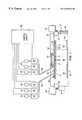
- FIG. 1is a cross-sectional view of the present invention chemical vapor deposition and etching apparatus
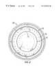
- FIG. 2is a top view of the gas distribution plate of the present invention chemical vapor deposition and etching apparatus.
- the chemical vapor deposition or dry etching apparatus 10 of the present inventionis depicted.
- the apparatusincludes a reaction chamber 12 having a chamber wall 14 constructed of a strong, rigid material that can be evacuated to lower atmospheric pressures.
- a vacuum pump 16is connected to the interior of the chamber 12 .
- a removable door or hatch 18is provided. The door 18 is firmly secured to the chamber wall 14 by way of a clamping member 20 .
- Vacuum seals 22are located between the door 18 and the chamber wall 14 to ensure that the chamber 12 is airtight to enable evacuation.
- a viewing window 23may be provided to allow visual contact with the interior of the chamber.
- a gas distribution plate 24is provided that is attached by way of fasteners such as screws, rivets or other attachment means to any interior surface of the vapor deposition chamber 12 .
- the gas distribution plate 24is attached to the interior surface of the door 18 of the chamber 12 but it could be attached to another interior surface of the chamber.
- the fasteners 26are placed through the fastener holes 28 on the gas distribution plate 24 and attach the gas distribution plate 24 to the door 18 .
- the gas distribution plate 24is a substantially flat structure that has a top and a bottom surface. In the preferred embodiment, the gas distribution plate 24 is circular although it could be rectangular or any other shape depending on the geometry of the chamber.
- the gas distribution plate 24has a plurality of apertures 30 that perforate the gas distribution plate 24 .
- FIG. 2depicts the apertures 30 arranged as a series of concentric circles, but other arrangements which provide a desirable distribution of vapor across the substrate 44 are within the scope of the invention.
- a gas-tight partition 32is disposed between the top surface of the gas distribution plate 24 and the interior surface of the door 18 of the reaction chamber.
- the partition 32defines two gas distribution zones 34 , 36 .
- the two dashed linesdepict the separation between the two gas distribution zones 34 and 36 .
- FIG. 1shows one partition 32 creating two gas distribution zones 34 and 36 , it is also contemplated that multiple partitions may be provided thereby creating three or more gas distribution zones.
- the partitiontakes the form of a rubber O-ring, but other types of partition structures are also possible.
- the partition 32could be integrally molded into the gas distribution plate 24 .
- the partitiondoes not have to be circular.
- Other shaped partitionscan be used so long as they distribute the gas in such a fashion to ensure a uniform rate of reaction across the substrate 44 .
- a uniform rate of reactionis desirable because it ensures a uniform growth rate of a film for the chemical vapor deposition process and a uniform removal rate for the dry etching process.
- a uniform rate of reactionis produced under ideal conditions by distributing the gas across the substrate 44 in an even distribution. However, due to factors such as uneven temperature or pressure gradients, the gases are required to be distributed across the substrate 44 in an uneven distribution.
- Two gas lines 38 and 40pass through the door 18 and into the reaction chamber 12 .
- One end of each of the gas lines 38 and 40is connected to each of the gas distribution zones 34 and 36 . Therefore, it will be understood that each of the gas lines 38 and 40 supply vapor to each of the gas distribution zones 34 and 36 .
- more than one partition 32is provided, it is contemplated that more than two gas lines may be provided.
- the other end of the gas lines 38 and 40are connected to a source of vapor 43 which could be a canister of gas or other suitable source of chemical vapor.
- Mass flow controllersshown in FIG. 1 as reference number 42 , are connected to each of the gas lines 38 and 40 .
- the mass flow regulators 42are typical prior art valves and can operate mechanically, electronically or pneumatically.
- Each of the mass flow controllers 42are connected to at least one control circuit 46 which operates to selectively open or close the mass flow controllers 42 .
- the mass flow controllers 42are used to regulate the flow of gas through each of the gas lines 38 and 40 . Therefore, the mass flow controllers 42 regulate the flow of gas to each of the gas distribution zones 34 and 36 . If one type of gas is to be deposited onto the substrate, then one mass flow controller 42 is provided for each gas line 38 and 40 . Alternatively, several mass flow controllers 42 may be provided if several different gases are to be supplied to deposit or dry etch onto the substrate.
- the chemical vapor deposition and etching apparatus of the present inventionoperates as follows.
- a wafer, substrate or work piece 44is introduced into the reaction chamber 12 and the chamber is closed. If desired, the vacuum pump 16 is employed to reduce the atmospheric pressure within the reaction chamber 12 .
- a source of vapor 43is provided and connected to the mass flow controllers 42 .
- the vaporis typically Ar, BCl 3 , Cl 2 , CF 3 Br, CHF 3 , CF 4 , C 2 F 6 , C 3 F 8 , CO, CCl 4 , HCl, HBr, NF 3 , O 2 or SF 6 , but other vapors (gases) are contemplated.
- the vaporflows through the gas lines 38 and 40 , and passes through the apertures 30 of the gas distribution plate 24 .
- the mass flow controllers 42are selectively controlled using the control circuit 46 to regulate the flow of vapor into each of the gas distribution zones 34 and 36 .
- the vaporflows over the wafer, substrate or work piece 44 and reacts at or near the surface of the substrate.
- the rate of flow of vaporis increased or decreased through each of the gas distribution zones 34 and 35 in order to produce a uniform rate of reaction across the surface of the substrate 44 .
Landscapes
- Chemical & Material Sciences (AREA)
- Engineering & Computer Science (AREA)
- General Chemical & Material Sciences (AREA)
- Chemical Kinetics & Catalysis (AREA)
- Materials Engineering (AREA)
- Mechanical Engineering (AREA)
- Metallurgy (AREA)
- Organic Chemistry (AREA)
- Physics & Mathematics (AREA)
- Condensed Matter Physics & Semiconductors (AREA)
- General Physics & Mathematics (AREA)
- Manufacturing & Machinery (AREA)
- Computer Hardware Design (AREA)
- Microelectronics & Electronic Packaging (AREA)
- Power Engineering (AREA)
- Drying Of Semiconductors (AREA)
- Chemical Vapour Deposition (AREA)
- ing And Chemical Polishing (AREA)
Abstract
Description
Claims (20)
Priority Applications (6)
| Application Number | Priority Date | Filing Date | Title |
|---|---|---|---|
| US08/756,670US6294026B1 (en) | 1996-11-26 | 1996-11-26 | Distribution plate for a reaction chamber with multiple gas inlets and separate mass flow control loops |
| TW086117263ATW514683B (en) | 1996-11-26 | 1997-11-19 | Distribution plate for a reaction chamber with multiple gas inlets and separate mass flow control loops |
| EP97309500AEP0844314B1 (en) | 1996-11-26 | 1997-11-25 | Recation chamber containing a gas distribution plate |
| DE69727536TDE69727536T2 (en) | 1996-11-26 | 1997-11-25 | Reaction chamber with built-in gas distributor plate |
| KR1019970062554AKR100530243B1 (en) | 1996-11-26 | 1997-11-25 | Distribution plate for a reaction chamber with multiple gas inlets and separate mass flow control loops |
| JP9324865AJPH10158844A (en) | 1996-11-26 | 1997-11-26 | Gas distribution plate for reaction chamber |
Applications Claiming Priority (1)
| Application Number | Priority Date | Filing Date | Title |
|---|---|---|---|
| US08/756,670US6294026B1 (en) | 1996-11-26 | 1996-11-26 | Distribution plate for a reaction chamber with multiple gas inlets and separate mass flow control loops |
Publications (1)
| Publication Number | Publication Date |
|---|---|
| US6294026B1true US6294026B1 (en) | 2001-09-25 |
Family
ID=25044535
Family Applications (1)
| Application Number | Title | Priority Date | Filing Date |
|---|---|---|---|
| US08/756,670Expired - LifetimeUS6294026B1 (en) | 1996-11-26 | 1996-11-26 | Distribution plate for a reaction chamber with multiple gas inlets and separate mass flow control loops |
Country Status (6)
| Country | Link |
|---|---|
| US (1) | US6294026B1 (en) |
| EP (1) | EP0844314B1 (en) |
| JP (1) | JPH10158844A (en) |
| KR (1) | KR100530243B1 (en) |
| DE (1) | DE69727536T2 (en) |
| TW (1) | TW514683B (en) |
Cited By (35)
| Publication number | Priority date | Publication date | Assignee | Title |
|---|---|---|---|---|
| US20020129768A1 (en)* | 2001-03-15 | 2002-09-19 | Carpenter Craig M. | Chemical vapor deposition apparatuses and deposition methods |
| US20020134309A1 (en)* | 1998-08-27 | 2002-09-26 | An-Chun Tu | Gas delivering device |
| US6508913B2 (en)* | 2000-10-06 | 2003-01-21 | Lam Research Corporation | Gas distribution apparatus for semiconductor processing |
| US20030230239A1 (en)* | 2002-06-17 | 2003-12-18 | Applied Materials, Inc. | Gas flow division in a wafer processing system having multiple chambers |
| US20040094092A1 (en)* | 2002-02-25 | 2004-05-20 | Derderian Garo J. | Apparatus for improved delivery of metastable species |
| US20040103844A1 (en)* | 2002-10-18 | 2004-06-03 | Chung-Yen Chou | [gas distributing system for delivering plasma gas to a wafer reaction chamber] |
| US6752166B2 (en) | 2001-05-24 | 2004-06-22 | Celerity Group, Inc. | Method and apparatus for providing a determined ratio of process fluids |
| US20040123806A1 (en)* | 2002-12-17 | 2004-07-01 | Anam Semiconductor Inc. | Chemical vapor deposition apparatus and method |
| US20040134611A1 (en)* | 2001-01-22 | 2004-07-15 | Tokyo Electron Limited | Plasma process system and plasma process method |
| US20040144310A1 (en)* | 2001-08-17 | 2004-07-29 | Campbell Philip H. | CVD apparatuses and methods of forming a layer over a semiconductor substrate |
| US6800139B1 (en)* | 1999-08-31 | 2004-10-05 | Tokyo Electron Limited | Film deposition apparatus and method |
| US20050001556A1 (en)* | 2002-07-09 | 2005-01-06 | Applied Materials, Inc. | Capacitively coupled plasma reactor with magnetic plasma control |
| US20050191416A1 (en)* | 2002-08-15 | 2005-09-01 | Cem Basceri | Methods of gas delivery for deposition processes and methods of depositing material on a substrate |
| US20050223984A1 (en)* | 2004-04-08 | 2005-10-13 | Hee-Gyoun Lee | Chemical vapor deposition (CVD) apparatus usable in the manufacture of superconducting conductors |
| US20050223983A1 (en)* | 2004-04-08 | 2005-10-13 | Venkat Selvamanickam | Chemical vapor deposition (CVD) apparatus usable in the manufacture of superconducting conductors |
| US20060000803A1 (en)* | 2002-11-26 | 2006-01-05 | Akira Koshiishi | Plasma processing method and apparatus |
| US20060027324A1 (en)* | 2004-08-03 | 2006-02-09 | Akitaka Makino | Plasma processing apparatus and plasma processing method |
| US20060062900A1 (en)* | 2004-09-21 | 2006-03-23 | Venkat Selvamanickam | Chemical vapor deposition (CVD) apparatus usable in the manufacture of superconducting conductors |
| US20080210377A1 (en)* | 2002-12-13 | 2008-09-04 | Lam Research Corporation | Uniform etch system |
| US20090014127A1 (en)* | 2007-07-12 | 2009-01-15 | Applied Materials, Inc. | Systems for plasma enhanced chemical vapor deposition and bevel edge etching |
| US20090061646A1 (en)* | 2007-09-05 | 2009-03-05 | Chiang Tony P | Vapor based combinatorial processing |
| US20090148704A1 (en)* | 2007-12-11 | 2009-06-11 | Sumitomo Electric Industries, Ltd. | Vapor-phase process apparatus, vapor-phase process method, and substrate |
| US20100104754A1 (en)* | 2008-10-24 | 2010-04-29 | Applied Materials, Inc. | Multiple gas feed apparatus and method |
| US20110006038A1 (en)* | 2009-07-13 | 2011-01-13 | Michael Charles Kutney | Plasma processing chamber with enhanced gas delivery |
| US20110100295A1 (en)* | 2002-04-16 | 2011-05-05 | Ming Xi | System and method for forming an integrated barrier layer |
| US8048806B2 (en) | 2000-03-17 | 2011-11-01 | Applied Materials, Inc. | Methods to avoid unstable plasma states during a process transition |
| US20130052346A1 (en)* | 2011-08-31 | 2013-02-28 | Alta Devices, Inc. | Cvd reactor with gas flow virtual walls |
| US8617351B2 (en) | 2002-07-09 | 2013-12-31 | Applied Materials, Inc. | Plasma reactor with minimal D.C. coils for cusp, solenoid and mirror fields for plasma uniformity and device damage reduction |
| US20140213068A1 (en)* | 2009-12-25 | 2014-07-31 | Tokyo Electron Limited | Film deposition apparatus and film deposition method |
| US10066297B2 (en) | 2011-08-31 | 2018-09-04 | Alta Devices, Inc. | Tiled showerhead for a semiconductor chemical vapor deposition reactor |
| US10249511B2 (en)* | 2014-06-27 | 2019-04-02 | Lam Research Corporation | Ceramic showerhead including central gas injector for tunable convective-diffusive gas flow in semiconductor substrate processing apparatus |
| CN111599720A (en)* | 2020-05-25 | 2020-08-28 | 上海华力集成电路制造有限公司 | Gas distributor |
| CN113293359A (en)* | 2020-02-24 | 2021-08-24 | 江苏鲁汶仪器有限公司 | PECVD gas homogenizing device capable of controlling gas inflow and proportion in a partitioned manner |
| US11447861B2 (en)* | 2016-12-15 | 2022-09-20 | Asm Ip Holding B.V. | Sequential infiltration synthesis apparatus and a method of forming a patterned structure |
| US11694911B2 (en)* | 2016-12-20 | 2023-07-04 | Lam Research Corporation | Systems and methods for metastable activated radical selective strip and etch using dual plenum showerhead |
Families Citing this family (16)
| Publication number | Priority date | Publication date | Assignee | Title |
|---|---|---|---|---|
| US5980686A (en) | 1998-04-15 | 1999-11-09 | Applied Komatsu Technology, Inc. | System and method for gas distribution in a dry etch process |
| US6489241B1 (en)* | 1999-09-17 | 2002-12-03 | Applied Materials, Inc. | Apparatus and method for surface finishing a silicon film |
| KR100464857B1 (en)* | 2002-08-26 | 2005-01-05 | 삼성전자주식회사 | Apparatus for etching edge of wafer |
| KR100513920B1 (en)* | 2003-10-31 | 2005-09-08 | 주식회사 시스넥스 | Chemical vapor deposition unit |
| US7892357B2 (en)* | 2004-01-12 | 2011-02-22 | Axcelis Technologies, Inc. | Gas distribution plate assembly for plasma reactors |
| JP4550507B2 (en) | 2004-07-26 | 2010-09-22 | 株式会社日立ハイテクノロジーズ | Plasma processing equipment |
| KR100820347B1 (en)* | 2006-12-27 | 2008-04-07 | 주식회사 선익시스템 | Gas injection device and substrate processing apparatus having the same |
| JP4963694B2 (en)* | 2008-09-29 | 2012-06-27 | 株式会社日立ハイテクノロジーズ | Plasma processing equipment |
| JP5452133B2 (en)* | 2009-08-27 | 2014-03-26 | 株式会社日立ハイテクノロジーズ | Plasma processing apparatus and plasma processing method |
| TWI399456B (en)* | 2010-01-25 | 2013-06-21 | Sun Well Solar Corp | Apparatus for conductive film coating and method for processing substrates therein |
| EP3357879A1 (en) | 2017-02-07 | 2018-08-08 | Heraeus Quarzglas GmbH & Co. KG | Gas distribution element for use in semiconductor manufacture and method for producing a gas distribution element |
| DE102017124456A1 (en) | 2017-10-19 | 2019-04-25 | Heraeus Noblelight Gmbh | Heatable gas injector |
| CN110484895B (en)* | 2018-05-14 | 2021-01-08 | 北京北方华创微电子装备有限公司 | Chamber assembly and reaction chamber |
| CN110468390B (en)* | 2019-08-02 | 2021-06-29 | 北方夜视技术股份有限公司 | Method for preparing functional film on inner wall of microchannel plate channel with super-large length-diameter ratio |
| JP7296523B2 (en)* | 2020-05-08 | 2023-06-22 | 株式会社ニューフレアテクノロジー | Deposition equipment and plate |
| CN116005130B (en)* | 2022-12-08 | 2025-08-15 | 浙江合特光电有限公司 | Air inlet and exhaust system of tubular CVD equipment |
Citations (8)
| Publication number | Priority date | Publication date | Assignee | Title |
|---|---|---|---|---|
| US3854443A (en)* | 1973-12-19 | 1974-12-17 | Intel Corp | Gas reactor for depositing thin films |
| US4256053A (en) | 1979-08-17 | 1981-03-17 | Dozier Alfred R | Chemical vapor reaction system |
| JPS60189928A (en)* | 1984-03-12 | 1985-09-27 | Fujitsu Ltd | Vapor growth device under reduced pressure |
| JPS615515A (en)* | 1984-06-07 | 1986-01-11 | Fujitsu Ltd | Chemical vapor growth apparatus |
| JPS6353932A (en)* | 1986-08-22 | 1988-03-08 | Nec Corp | Apparatus for growing thin film semiconductor wafer |
| US5453124A (en)* | 1992-12-30 | 1995-09-26 | Texas Instruments Incorporated | Programmable multizone gas injector for single-wafer semiconductor processing equipment |
| US5755886A (en)* | 1986-12-19 | 1998-05-26 | Applied Materials, Inc. | Apparatus for preventing deposition gases from contacting a selected region of a substrate during deposition processing |
| US5781693A (en)* | 1996-07-24 | 1998-07-14 | Applied Materials, Inc. | Gas introduction showerhead for an RTP chamber with upper and lower transparent plates and gas flow therebetween |
Family Cites Families (7)
| Publication number | Priority date | Publication date | Assignee | Title |
|---|---|---|---|---|
| US3381114A (en)* | 1963-12-28 | 1968-04-30 | Nippon Electric Co | Device for manufacturing epitaxial crystals |
| JPS5687328A (en)* | 1979-12-18 | 1981-07-15 | Matsushita Electronics Corp | Semiconductor treatment device |
| JPS62172727A (en)* | 1986-01-27 | 1987-07-29 | Hitachi Ltd | surface treatment equipment |
| DE69227575T2 (en)* | 1991-12-30 | 1999-06-02 | Texas Instruments Inc | Programmable multi-zone gas injector for a system for the treatment of individual semiconductor wafers |
| JPH0778769A (en)* | 1993-09-07 | 1995-03-20 | Fuji Xerox Co Ltd | Semiconductor manufacturing equipment |
| EP0648858A1 (en)* | 1993-10-15 | 1995-04-19 | Applied Materials, Inc. | Methods of coating plasma etch chambers and apparatus for plasma etching workpieces |
| JP3360098B2 (en)* | 1995-04-20 | 2002-12-24 | 東京エレクトロン株式会社 | Shower head structure of processing equipment |
- 1996
- 1996-11-26USUS08/756,670patent/US6294026B1/ennot_activeExpired - Lifetime
- 1997
- 1997-11-19TWTW086117263Apatent/TW514683B/ennot_activeIP Right Cessation
- 1997-11-25EPEP97309500Apatent/EP0844314B1/ennot_activeExpired - Lifetime
- 1997-11-25KRKR1019970062554Apatent/KR100530243B1/ennot_activeExpired - Fee Related
- 1997-11-25DEDE69727536Tpatent/DE69727536T2/ennot_activeExpired - Lifetime
- 1997-11-26JPJP9324865Apatent/JPH10158844A/ennot_activeWithdrawn
Patent Citations (8)
| Publication number | Priority date | Publication date | Assignee | Title |
|---|---|---|---|---|
| US3854443A (en)* | 1973-12-19 | 1974-12-17 | Intel Corp | Gas reactor for depositing thin films |
| US4256053A (en) | 1979-08-17 | 1981-03-17 | Dozier Alfred R | Chemical vapor reaction system |
| JPS60189928A (en)* | 1984-03-12 | 1985-09-27 | Fujitsu Ltd | Vapor growth device under reduced pressure |
| JPS615515A (en)* | 1984-06-07 | 1986-01-11 | Fujitsu Ltd | Chemical vapor growth apparatus |
| JPS6353932A (en)* | 1986-08-22 | 1988-03-08 | Nec Corp | Apparatus for growing thin film semiconductor wafer |
| US5755886A (en)* | 1986-12-19 | 1998-05-26 | Applied Materials, Inc. | Apparatus for preventing deposition gases from contacting a selected region of a substrate during deposition processing |
| US5453124A (en)* | 1992-12-30 | 1995-09-26 | Texas Instruments Incorporated | Programmable multizone gas injector for single-wafer semiconductor processing equipment |
| US5781693A (en)* | 1996-07-24 | 1998-07-14 | Applied Materials, Inc. | Gas introduction showerhead for an RTP chamber with upper and lower transparent plates and gas flow therebetween |
Cited By (73)
| Publication number | Priority date | Publication date | Assignee | Title |
|---|---|---|---|---|
| US20020134309A1 (en)* | 1998-08-27 | 2002-09-26 | An-Chun Tu | Gas delivering device |
| US6828246B2 (en)* | 1998-08-27 | 2004-12-07 | Winbond Electronics Corp. | Gas delivering device |
| US6800139B1 (en)* | 1999-08-31 | 2004-10-05 | Tokyo Electron Limited | Film deposition apparatus and method |
| US8048806B2 (en) | 2000-03-17 | 2011-11-01 | Applied Materials, Inc. | Methods to avoid unstable plasma states during a process transition |
| US20070251920A1 (en)* | 2000-03-17 | 2007-11-01 | Hoffman Daniel J | Method of operating a plasma reactor having an overhead electrode with a fixed impedance match element |
| US6508913B2 (en)* | 2000-10-06 | 2003-01-21 | Lam Research Corporation | Gas distribution apparatus for semiconductor processing |
| US7481886B2 (en)* | 2001-01-22 | 2009-01-27 | Tokyo Electron Limited | Plasma process system and plasma process method |
| US20040134611A1 (en)* | 2001-01-22 | 2004-07-15 | Tokyo Electron Limited | Plasma process system and plasma process method |
| US20050241581A1 (en)* | 2001-03-15 | 2005-11-03 | Carpenter Craig M | Chemical vapor deposition apparatuses and deposition methods |
| US20020129768A1 (en)* | 2001-03-15 | 2002-09-19 | Carpenter Craig M. | Chemical vapor deposition apparatuses and deposition methods |
| US7424894B2 (en) | 2001-05-24 | 2008-09-16 | Celerity, Inc. | Method and apparatus for providing a determined ratio of process fluids |
| US6941965B2 (en) | 2001-05-24 | 2005-09-13 | Celerity, Inc. | Method and apparatus for providing a determined ratio of process fluids |
| US20070107783A1 (en)* | 2001-05-24 | 2007-05-17 | Lull John M | Method and apparatus for providing a determined ratio of process fluids |
| US7143774B2 (en) | 2001-05-24 | 2006-12-05 | Celerity, Inc. | Method and apparatus for providing a determined ratio of process fluids |
| US20040200529A1 (en)* | 2001-05-24 | 2004-10-14 | Celerity Group, Inc. | Method and apparatus for providing a determined ratio of process fluids |
| US6752166B2 (en) | 2001-05-24 | 2004-06-22 | Celerity Group, Inc. | Method and apparatus for providing a determined ratio of process fluids |
| US7360551B2 (en) | 2001-05-24 | 2008-04-22 | Celerity, Inc. | Method and apparatus for providing a determined ratio of process fluids |
| US20050241698A1 (en)* | 2001-05-24 | 2005-11-03 | Lull John M | Method and apparatus for providing a determined ratio of process fluids |
| US20040144310A1 (en)* | 2001-08-17 | 2004-07-29 | Campbell Philip H. | CVD apparatuses and methods of forming a layer over a semiconductor substrate |
| US20050112890A1 (en)* | 2001-08-17 | 2005-05-26 | Campbell Philip H. | CVD apparatuses and methods of forming a layer over a semiconductor substrate |
| US6849133B2 (en)* | 2001-08-17 | 2005-02-01 | Micron Technology, Inc. | CVD apparatuses and methods of forming a layer over a semiconductor substrate |
| US20040213908A1 (en)* | 2002-02-25 | 2004-10-28 | Derderian Garo J. | Deposition methods and apparatus for improved delivery of metastable species |
| US7527693B2 (en) | 2002-02-25 | 2009-05-05 | Micron Technology, Inc. | Apparatus for improved delivery of metastable species |
| US20040094092A1 (en)* | 2002-02-25 | 2004-05-20 | Derderian Garo J. | Apparatus for improved delivery of metastable species |
| US7393562B2 (en) | 2002-02-25 | 2008-07-01 | Micron Technology, Inc. | Deposition methods for improved delivery of metastable species |
| US20110100295A1 (en)* | 2002-04-16 | 2011-05-05 | Ming Xi | System and method for forming an integrated barrier layer |
| US7955986B2 (en) | 2002-05-22 | 2011-06-07 | Applied Materials, Inc. | Capacitively coupled plasma reactor with magnetic plasma control |
| US6913652B2 (en) | 2002-06-17 | 2005-07-05 | Applied Materials, Inc. | Gas flow division in a wafer processing system having multiple chambers |
| US20030230239A1 (en)* | 2002-06-17 | 2003-12-18 | Applied Materials, Inc. | Gas flow division in a wafer processing system having multiple chambers |
| US8617351B2 (en) | 2002-07-09 | 2013-12-31 | Applied Materials, Inc. | Plasma reactor with minimal D.C. coils for cusp, solenoid and mirror fields for plasma uniformity and device damage reduction |
| US20050001556A1 (en)* | 2002-07-09 | 2005-01-06 | Applied Materials, Inc. | Capacitively coupled plasma reactor with magnetic plasma control |
| US20080023143A1 (en)* | 2002-07-09 | 2008-01-31 | Hoffman Daniel J | Capacitively coupled plasma reactor with magnetic plasma control |
| US7399499B2 (en) | 2002-08-15 | 2008-07-15 | Micron Technology, Inc. | Methods of gas delivery for deposition processes and methods of depositing material on a substrate |
| US20050191416A1 (en)* | 2002-08-15 | 2005-09-01 | Cem Basceri | Methods of gas delivery for deposition processes and methods of depositing material on a substrate |
| US20040103844A1 (en)* | 2002-10-18 | 2004-06-03 | Chung-Yen Chou | [gas distributing system for delivering plasma gas to a wafer reaction chamber] |
| US20060000803A1 (en)* | 2002-11-26 | 2006-01-05 | Akira Koshiishi | Plasma processing method and apparatus |
| US8512510B2 (en) | 2002-11-26 | 2013-08-20 | Tokyo Electron Limited | Plasma processing method and apparatus |
| US20100043974A1 (en)* | 2002-11-26 | 2010-02-25 | Akira Koshiishi | Plasma processing method and apparatus |
| US20110214813A1 (en)* | 2002-11-26 | 2011-09-08 | Akira Koshiishi | Plasma processing method and apparatus |
| US8801892B2 (en)* | 2002-12-13 | 2014-08-12 | Lam Research Corporation | Uniform etch system |
| US20080210377A1 (en)* | 2002-12-13 | 2008-09-04 | Lam Research Corporation | Uniform etch system |
| US20040123806A1 (en)* | 2002-12-17 | 2004-07-01 | Anam Semiconductor Inc. | Chemical vapor deposition apparatus and method |
| US7347900B2 (en)* | 2002-12-17 | 2008-03-25 | Dongbu Electronics Co., Ltd. | Chemical vapor deposition apparatus and method |
| US7910155B2 (en) | 2004-04-08 | 2011-03-22 | Superpower, Inc. | Method for manufacturing high temperature superconducting conductor |
| US20050223983A1 (en)* | 2004-04-08 | 2005-10-13 | Venkat Selvamanickam | Chemical vapor deposition (CVD) apparatus usable in the manufacture of superconducting conductors |
| US20050223984A1 (en)* | 2004-04-08 | 2005-10-13 | Hee-Gyoun Lee | Chemical vapor deposition (CVD) apparatus usable in the manufacture of superconducting conductors |
| US20100009064A1 (en)* | 2004-04-08 | 2010-01-14 | Superpower, Inc. | Chemical vapor deposition (CVD) apparatus usable in the manufacture of superconducting conductors |
| US8268386B2 (en) | 2004-04-08 | 2012-09-18 | Superpower Inc. | Method for manufacturing high-temperature superconducting conductors |
| US20060027324A1 (en)* | 2004-08-03 | 2006-02-09 | Akitaka Makino | Plasma processing apparatus and plasma processing method |
| US20090001052A1 (en)* | 2004-08-03 | 2009-01-01 | Akitaka Makino | Plasma processing apparatus and plasma processing method |
| US7387811B2 (en) | 2004-09-21 | 2008-06-17 | Superpower, Inc. | Method for manufacturing high temperature superconducting conductors using chemical vapor deposition (CVD) |
| US20060062900A1 (en)* | 2004-09-21 | 2006-03-23 | Venkat Selvamanickam | Chemical vapor deposition (CVD) apparatus usable in the manufacture of superconducting conductors |
| KR101354571B1 (en) | 2007-07-12 | 2014-01-23 | 어플라이드 머티어리얼스, 인코포레이티드 | Systems for plasma enhanced chemical vapor deposition and bevel edge etching |
| US8197636B2 (en)* | 2007-07-12 | 2012-06-12 | Applied Materials, Inc. | Systems for plasma enhanced chemical vapor deposition and bevel edge etching |
| US20090014127A1 (en)* | 2007-07-12 | 2009-01-15 | Applied Materials, Inc. | Systems for plasma enhanced chemical vapor deposition and bevel edge etching |
| US20090061646A1 (en)* | 2007-09-05 | 2009-03-05 | Chiang Tony P | Vapor based combinatorial processing |
| US20090148704A1 (en)* | 2007-12-11 | 2009-06-11 | Sumitomo Electric Industries, Ltd. | Vapor-phase process apparatus, vapor-phase process method, and substrate |
| US8349403B2 (en) | 2007-12-11 | 2013-01-08 | Sumitomo Electric Industries, Ltd. | Vapor-phase process apparatus, vapor-phase process method, and substrate |
| US8349083B2 (en) | 2007-12-11 | 2013-01-08 | Sumitomo Electric Industries, Ltd. | Vapor-phase process apparatus, vapor-phase process method, and substrate |
| US8628616B2 (en)* | 2007-12-11 | 2014-01-14 | Sumitomo Electric Industries, Ltd. | Vapor-phase process apparatus, vapor-phase process method, and substrate |
| US20100104754A1 (en)* | 2008-10-24 | 2010-04-29 | Applied Materials, Inc. | Multiple gas feed apparatus and method |
| US8382939B2 (en) | 2009-07-13 | 2013-02-26 | Applied Materials, Inc. | Plasma processing chamber with enhanced gas delivery |
| WO2011008703A3 (en)* | 2009-07-13 | 2011-04-28 | Applied Materials, Inc. | Plasma processing chamber with enhanced gas delivery |
| US20110006038A1 (en)* | 2009-07-13 | 2011-01-13 | Michael Charles Kutney | Plasma processing chamber with enhanced gas delivery |
| US20140213068A1 (en)* | 2009-12-25 | 2014-07-31 | Tokyo Electron Limited | Film deposition apparatus and film deposition method |
| US20130052346A1 (en)* | 2011-08-31 | 2013-02-28 | Alta Devices, Inc. | Cvd reactor with gas flow virtual walls |
| US9212422B2 (en)* | 2011-08-31 | 2015-12-15 | Alta Devices, Inc. | CVD reactor with gas flow virtual walls |
| US10066297B2 (en) | 2011-08-31 | 2018-09-04 | Alta Devices, Inc. | Tiled showerhead for a semiconductor chemical vapor deposition reactor |
| US10249511B2 (en)* | 2014-06-27 | 2019-04-02 | Lam Research Corporation | Ceramic showerhead including central gas injector for tunable convective-diffusive gas flow in semiconductor substrate processing apparatus |
| US11447861B2 (en)* | 2016-12-15 | 2022-09-20 | Asm Ip Holding B.V. | Sequential infiltration synthesis apparatus and a method of forming a patterned structure |
| US11694911B2 (en)* | 2016-12-20 | 2023-07-04 | Lam Research Corporation | Systems and methods for metastable activated radical selective strip and etch using dual plenum showerhead |
| CN113293359A (en)* | 2020-02-24 | 2021-08-24 | 江苏鲁汶仪器有限公司 | PECVD gas homogenizing device capable of controlling gas inflow and proportion in a partitioned manner |
| CN111599720A (en)* | 2020-05-25 | 2020-08-28 | 上海华力集成电路制造有限公司 | Gas distributor |
Also Published As
| Publication number | Publication date |
|---|---|
| EP0844314A3 (en) | 2001-04-11 |
| EP0844314B1 (en) | 2004-02-11 |
| DE69727536T2 (en) | 2004-12-23 |
| DE69727536D1 (en) | 2004-03-18 |
| JPH10158844A (en) | 1998-06-16 |
| TW514683B (en) | 2002-12-21 |
| KR19980042712A (en) | 1998-08-17 |
| EP0844314A2 (en) | 1998-05-27 |
| KR100530243B1 (en) | 2006-01-27 |
Similar Documents
| Publication | Publication Date | Title |
|---|---|---|
| US6294026B1 (en) | Distribution plate for a reaction chamber with multiple gas inlets and separate mass flow control loops | |
| CN1186873A (en) | Distribution plate for reaction chamber with multiple gas inlets and separate mass flow control loops | |
| US6040011A (en) | Substrate support member with a purge gas channel and pumping system | |
| US20060011298A1 (en) | Showerhead with branched gas receiving channel and apparatus including the same for use in manufacturing semiconductor substrates | |
| US7829145B2 (en) | Methods of uniformity control for low flow process and chamber to chamber matching | |
| US11031262B2 (en) | Loadlock integrated bevel etcher system | |
| US12237182B2 (en) | Showerhead device for semiconductor processing system | |
| KR20060096460A (en) | Gas distribution showerhead featuring an exhaust opening | |
| KR20180126086A (en) | Micro-volume deposition chamber | |
| US8758511B2 (en) | Film forming apparatus and vaporizer | |
| JP2020501020A (en) | Thin film encapsulation processing system and process kit | |
| US20220154338A1 (en) | Apparatus and system for delivering gas to a process chamber | |
| US20190338420A1 (en) | Pressure skew system for controlling center-to-edge pressure change | |
| US20230137026A1 (en) | Method and system for selectively removing material at an edge of a substrate | |
| US20200098549A1 (en) | Heat conductive spacer for plasma processing chamber | |
| TW202213426A (en) | Remote-plasma clean (rpc) directional-flow device | |
| JPH0341722A (en) | Thin-film manufacturing apparatus | |
| KR20230151914A (en) | Substrate Processing Apparatus including Exhaust Duct | |
| KR20230042572A (en) | Gas-phase reactor system and method of cleaning same | |
| KR200429542Y1 (en) | Plasma processing apparatus for flat panel display substrate processing | |
| KR20240154608A (en) | Deposition apparatus, substrate processing system, and method for processing substrates |
Legal Events
| Date | Code | Title | Description |
|---|---|---|---|
| AS | Assignment | Owner name:SIEMENS COMPONENTS, INC., CALIFORNIA Free format text:ASSIGNMENT OF ASSIGNORS INTEREST;ASSIGNOR:POSCHENRIEDER, BERNHARD;REEL/FRAME:008325/0681 Effective date:19960917 Owner name:INTERNATIONAL BUSINESS MACHINES CORPORATION, NEW Y Free format text:ASSIGNMENT OF ASSIGNORS INTEREST;ASSIGNOR:MULLER, KARL PAUL;REEL/FRAME:008325/0696 Effective date:19960909 Owner name:SIEMENS COMPONENTS, INC., CALIFORNIA Free format text:ASSIGNMENT OF ASSIGNORS INTEREST;ASSIGNOR:ROITHNER, KLAUS;REEL/FRAME:008325/0711 Effective date:19960910 | |
| AS | Assignment | Owner name:SIEMENS AKTIENGESELLSCHAFT, GERMANY Free format text:ASSIGNMENT OF ASSIGNORS INTEREST;ASSIGNOR:SIEMENS COMPONENTS, INC.;REEL/FRAME:008451/0834 Effective date:19970408 | |
| DJ | All references should be deleted, no patent was granted | ||
| WDR | Patent withdrawn according to listing issued by the uspto on prs-date | ||
| STCF | Information on status: patent grant | Free format text:PATENTED CASE | |
| AS | Assignment | Owner name:INFINEON TECHNOLOGIES AG, GERMANY Free format text:ASSIGNMENT OF ASSIGNORS INTEREST;ASSIGNOR:SIEMENS AKTIENGESELLSCHAFT;REEL/FRAME:015386/0643 Effective date:20041026 | |
| FPAY | Fee payment | Year of fee payment:4 | |
| REMI | Maintenance fee reminder mailed | ||
| FPAY | Fee payment | Year of fee payment:8 | |
| SULP | Surcharge for late payment | Year of fee payment:7 | |
| AS | Assignment | Owner name:QIMONDA AG,GERMANY Free format text:ASSIGNMENT OF ASSIGNORS INTEREST;ASSIGNOR:INFINEON TECHNOLOGIES AG;REEL/FRAME:023768/0001 Effective date:20060425 Owner name:QIMONDA AG, GERMANY Free format text:ASSIGNMENT OF ASSIGNORS INTEREST;ASSIGNOR:INFINEON TECHNOLOGIES AG;REEL/FRAME:023768/0001 Effective date:20060425 | |
| FPAY | Fee payment | Year of fee payment:12 | |
| AS | Assignment | Owner name:INFINEON TECHNOLOGIES AG, GERMANY Free format text:ASSIGNMENT OF ASSIGNORS INTEREST;ASSIGNOR:QIMONDA AG;REEL/FRAME:035623/0001 Effective date:20141009 |