US6292766B1 - Simulation tool input file generator for interface circuitry - Google Patents
Simulation tool input file generator for interface circuitryDownload PDFInfo
- Publication number
- US6292766B1 US6292766B1US09/216,385US21638598AUS6292766B1US 6292766 B1US6292766 B1US 6292766B1US 21638598 AUS21638598 AUS 21638598AUS 6292766 B1US6292766 B1US 6292766B1
- Authority
- US
- United States
- Prior art keywords
- simulation tool
- tool input
- input file
- simulation
- file
- Prior art date
- Legal status (The legal status is an assumption and is not a legal conclusion. Google has not performed a legal analysis and makes no representation as to the accuracy of the status listed.)
- Expired - Lifetime
Links
Images


Classifications
- G—PHYSICS
- G06—COMPUTING OR CALCULATING; COUNTING
- G06F—ELECTRIC DIGITAL DATA PROCESSING
- G06F30/00—Computer-aided design [CAD]
- G06F30/30—Circuit design
- G06F30/36—Circuit design at the analogue level
- G06F30/367—Design verification, e.g. using simulation, simulation program with integrated circuit emphasis [SPICE], direct methods or relaxation methods
- Y—GENERAL TAGGING OF NEW TECHNOLOGICAL DEVELOPMENTS; GENERAL TAGGING OF CROSS-SECTIONAL TECHNOLOGIES SPANNING OVER SEVERAL SECTIONS OF THE IPC; TECHNICAL SUBJECTS COVERED BY FORMER USPC CROSS-REFERENCE ART COLLECTIONS [XRACs] AND DIGESTS
- Y10—TECHNICAL SUBJECTS COVERED BY FORMER USPC
- Y10S—TECHNICAL SUBJECTS COVERED BY FORMER USPC CROSS-REFERENCE ART COLLECTIONS [XRACs] AND DIGESTS
- Y10S706/00—Data processing: artificial intelligence
- Y10S706/902—Application using ai with detail of the ai system
- Y10S706/919—Designing, planning, programming, CAD, CASE
- Y10S706/921—Layout, e.g. circuit, construction
- Y—GENERAL TAGGING OF NEW TECHNOLOGICAL DEVELOPMENTS; GENERAL TAGGING OF CROSS-SECTIONAL TECHNOLOGIES SPANNING OVER SEVERAL SECTIONS OF THE IPC; TECHNICAL SUBJECTS COVERED BY FORMER USPC CROSS-REFERENCE ART COLLECTIONS [XRACs] AND DIGESTS
- Y10—TECHNICAL SUBJECTS COVERED BY FORMER USPC
- Y10S—TECHNICAL SUBJECTS COVERED BY FORMER USPC CROSS-REFERENCE ART COLLECTIONS [XRACs] AND DIGESTS
- Y10S715/00—Data processing: presentation processing of document, operator interface processing, and screen saver display processing
- Y10S715/961—Operator interface with visual structure or function dictated by intended use
- Y10S715/964—CAD or CAM, e.g. interactive design tools
Definitions
- the present inventionrelates to the field of electrical circuit simulation tools. More particularly, the present invention relates to a simulation tool input file generator that constructs input files for performing design analysis of electrical circuits such as input/output buffer rings in a microelectronic chip.
- a chip designerusually tries to reach an optimal balance in which there are a minimum number of power and ground IO buffer circuit connections taking up valuable chip space while at the same time ensuring there are enough power and ground IO buffer circuit connections to prevent noise interference from exceeding an acceptable level.
- Analyzing potential noise interference in an IO buffer circuitis typically complicated by a variety of factors. Usually, there are numerous IO buffer circuits in a chip and the sheer quantity result in the expenditure of significant resources to analyze noise contributions in IO buffer circuits. This large quantity of IO buffer circuits usually comprises a variety of switching configurations that have different electrical characteristics for each specific load. A number of internal and external electrical characteristics, such as resistance, capacitance, inductance, mutual inductance, etc., contribute to noise generation and its adverse affects on a signal in an IO buffer circuit. An analysis of noise in IO buffer circuits should be performed dynamically in a manner that is cognizant of affects resulting from internal and external changes in electrical characteristics and the relative location of one IO buffer to other IO buffers. Thus, the complexity of an accurate analysis of adverse impacts due to noise interference in an IO buffer circuit requires significant resources.
- CAE design toolsare general-purpose simulation software programs that perform such functions as nonlinear DC analysis, nonlinear transient analysis, and linear AC analysis of electrical signals, while others are directed more to specific types of analysis.
- Circuits being designed or analyzedusually include resistors, capacitors, inductors, voltage and current sources, switches, uniform distributed RC lines, and common semiconductor devices such as bipolar junction transistors (BJT), junction field effect transistors (JFET), metal oxide surface field effect transistors (MOSFET), etc.
- BJTbipolar junction transistors
- JFETjunction field effect transistors
- MOSFETmetal oxide surface field effect transistors
- Analyzing an electronic system or circuit with multiple simulation toolsusually provides better results and greater insight into performance abilities than a single simulation tool can provide.
- different simulation tool familiesprovide different benefits.
- two common simulation software toolsinclude simulation programs with integrated circuit emphasis (SPICE) and input/output buffer information specifications (IBIS). SPICE and IBIS simulation tools provide different advantages.
- SPICE toolstypically permit detailed electrical analysis of circuits including integrated circuit chips.
- SPICE simulatorsare capable of performing device generated noise analysis for a given circuit including IO buffer circuits.
- a SPICE simulatoris capable of calculating a value of the noise corresponding to a spectral density of a circuit variable viewed as a stationary gaussian stochastic. After calculating spectral densities, the values are integrated over the specified frequency range to arrive at the total noise voltage/current.
- IBIS descriptionsprovide a “black box” behavioral model of an IO buffer circuit. Direct current versus voltage (IN) curves, rise and fall time, and packaging information are fed into an IBIS simulation tool. IBIS simulations are advantageous for a number of reasons including being well suited for simulating an entire electronic system of several hundred nets and drivers, presenting signal integrity or flight-time information in a relatively practical manner and quickly completing simulations.
- IBIS simulationsare advantageous for a number of reasons including being well suited for simulating an entire electronic system of several hundred nets and drivers, presenting signal integrity or flight-time information in a relatively practical manner and quickly completing simulations.
- Simulation tool input filesprovided by the system and method should include electrical component description simulation tool input files and electrical characteristic description simulation tool input files such as SPICE formatted input files and IBIS formatted input files. These simulation input files should permit detailed signal integrity analysis and characterization of internal and external signals in one simulation session.
- the system and methodshould economically generate simulation tool input files of a chip's interface circuitry in a manner that allows the use of simulation tools to design and analyze an IO buffer circuit ring integrated on an electronic chip.
- the present inventionprovides these advantageous features.
- the present inventionis a system and method that permits a designer to efficiently and effectively create and modify electrical circuit simulation tool input files.
- the system and methodenables a user to conveniently convey information in a manner that minimizes the amount of data a user has to manually enter while adequately describing features of the circuit being designed or analyzed. It allows a user to easily modify design features without manually modifying the entire simulation input file and is capable of producing electrical component description simulation tool input files and electrical characteristic description simulation tool input files.
- the present inventionis capable of providing simulation input files with enough information to permit detailed signal integrity analysis and characterization of internal and external signals in one simulation session. For example, the system and method economically generates simulation tool input files of a chip's interface circuitry in a manner that allows the use of SPICE and IBIS simulation tools to design and analyze an IO buffer circuit ring integrated on an electronic chip.
- an electrical circuit simulation tool input file generatoris implemented in a computer system.
- the input file generatorincludes a user friendly graphical interface for selecting circuit description files and modifying values assigned to fields in an instance of the circuit description file.
- Detailed input files compatible with simulation tool formatsare generated by the present invention and automatically populated with appropriate values for electrical characteristics based upon referenced circuit description files and special user modification notations.
- FIG. 1Ais a block diagram representation of one embodiment of the present invention.
- FIG. 1Billustrates a computer system utilized by the present invention.
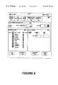
- FIG. 2is an illustration of one embodiment of a graphical user interface generated by a user interface module of the present invention showing a main window.
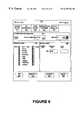
- FIG. 3is an illustration of one embodiment of a GUI displaying a design setup subwindow of the present invention.
- FIG. 4is an example of a floor plan file setting forth an input/output buffer circuit floor plan for a chip in accordance with the present invention.
- FIG. 5is a schematic illustrating the placement of IO buffer circuits in a typical IO buffer ring in accordance with the present invention.
- FIG. 6is an exemplary IO buffer circuit description file in accordance with the present invention, which in the particular embodiment shown is an output only buffer circuit.
- FIG. 7is an illustration of a design setup subwindow of the present invention with a display listing power lines coupled to IO buffer circuits.
- FIG. 8shows IO definition subwindow in accordance with the present invention illustrating information regarding IO buffer circuit in slot 1 of a chip.
- FIG. 9is an illustration depicting IO definition subwindow in accordance with the present invention associated with IO buffer circuit assigned to slot 47 of a chip.
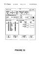
- FIG. 10is an illustration of IO definition subwindow in accordance with the present invention for slot 4 of a electrical chip.
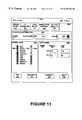
- FIG. 11is an illustration of IO definition subwindow in accordance with the present invention for slot 4 of a chip selected after a user has deselected some lines by clicking on right connection indicators.
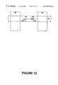
- FIG. 12is a symbolic illustration of internal electrical characteristics of buses coupled to IO buffer circuits.
- FIG. 13is a symbolic illustration of electrical characteristics associated with a lead coupled between a pad and a pin.
- FIG. 14illustrates load setup subwindow in accordance with the present invention depicting values assigned to internal electrical characteristics of buses coupled to IO buffer circuits.
- FIG. 15is an example of one embodiment of simulation control subwindow in accordance with the present invention showing values assigned to control information and pin capacitive load.
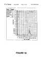
- FIG. 16is a graph illustrating noise in a VSS and VDD power line of one IO buffer configuration analyzed using IOSim in accordance with the present invention.
- FIG. 17illustrates a symbolic representation of elements included in an IBIS model of an electrical IO buffer circuit, a pad and a pin.
- FIG. 18is a partial listing of an IBIS model file included in a library of electrical characteristic models folder in accordance with the present invention.
- FIG. 19is a partial listing of a SPICE simulation tool input file.
- FIG. 20is a flow chart of one embodiment of an IOSim method in accordance with the present invention.
- the present inventionpermits a designer to efficiently and effectively create and modify electrical circuit simulation tool input files.
- the present system and methodenables a user to convey information conveniently in a manner that minimizes the amount of data a user has to enter manually while adequately describing features of the circuit being designed or analyzed. It allows a user to easily modify design features without manually modifying the entire simulation input file.
- the present inventionprovides electrical component description simulation tool input files and electrical characteristic description simulation input files such as SPICE formatted sub-circuit description files and IBIS formatted input files.
- the simulation tool input files generator of the present inventionis capable of providing detailed files sufficient for use in signal integrity analysis and characterization of internal and external signals in one simulation session. For example, the system and method of the present invention economically generates simulation input files of an integrated circuit chip's interface circuitry in a manner that allows the use of simulation tools to design and analyze an IO buffer circuit ring.
- FIG. 1Ais a logical block diagram of a system 109 including one embodiment of the present invention IOSim 100 .
- IOSim 100is a software program operating on a computer system including a processor coupled to a bus and a memory coupled the bus. In another embodiment, operations of IOSim 100 are implemented in hardware.
- IOSim 100comprises a user interface module 110 , electrical component model generator 120 and electrical characteristic (e.g. IBIS) model generator 130 .
- IOSim 100is coupled to various description file folders comprising a block description of chip interface folder 141 , library of electrical circuit description folder 142 , silicon technology information folder 143 , package technology information folder 144 , library of circuit electrical characteristics folder 145 , electrical component description folder 151 and electrical characteristic description folder 152 .
- IOSim 100generates simulation tool input files within IOSim 100 is typically an iterative process involving both activities performed by IOSim 100 and inputs from a user.
- IOSim 100facilitates communications between a user and IOSim 100 in a manner that is described below.
- a userbegins by defining a design at a high level and setting forth some basic parameters. Based upon the information provided by a user, IOSim 100 retrieves appropriate information from other sources such as library or information folders. IOSim 100 then processes the information and generates a detailed description of a circuit or system being analyzed. Usually there are points in the process at which a user has opportunities to provide additional information or modify the information assembled and arranged by IOSim 100 .
- IOSim 100When a user is satisfied that appropriate information has been incorporated to perform a design analysis, IOSim 100 generates a simulation tool input file.
- User interface module 110 of FIG. 1Aenables a user to communicate expediently and efficiently with electrical component model generator 120 and electrical characteristic model generator 130 .
- user interface module 110comprises software code that generates an interactive graphical user interface (GUI).
- GUIgraphical user interface
- the GUIpresents information regarding operations of IOSim 100 to the user.
- user interface module 110interprets batch code text rather than relying on GUI input.
- User interface module 110conveys information between a user and other components of IOSim 100 in a convenient format that is easier to read and modify relative to a complex simulation tool formatted input text.
- Electrical component model generator 120creates complex electrical component description files based upon information supplied by a user via user interface module 110 . Electrical component model generator 120 interprets information and commands transmitted from user interface module 110 and performs complex iterations required to generate an electrical component description simulation input file. For example, electrical component model generator 120 locates and retrieves files identified via a GUI, such as files from block description of chip interface folder 141 , library of electrical circuit description folder 142 , silicon technology information folder 143 , package technology information folder 144 , etc. After retrieving identified files, electrical component model generator 120 creates a collection of electrical simulation tool formatted input files in an appropriate arrangement.
- electrical component model generator 120arranges circuit description files in a particular order identified in a floor file retrieved from block description of chip interface folder 141 and creates multiple instances of a circuit description file if required.
- a floor fileis a text file listing names of IO buffer circuit description files in order according to the position of the corresponding IO buffer in an IO interface of an integrated circuit chip.
- Electrical component model generator 120also populates these electrical simulation tool formatted files with appropriate data and creates any additional electrical simulation input files required to adequately describe a circuit being analyzed.
- Electrical characteristic model generator 130 of FIG. 1creates complex electrical characteristic description files based upon information supplied by a user via user interface module 110 .
- Electrical characteristic model generator 130is similar to electrical component model generator 120 except it is concerned with producing electrical characteristic description files instead of electrical component description simulation tool input files. It also interprets information and commands from the GUI in an easy to use format and performs complex iterations directed at forming a board level simulation tool input file. For example, electrical characteristic model generator 130 locates and retrieves files identified by a user via a GUI, arranges electrical characteristic simulation tool formatted files in a specified order, populates these files with appropriate data and creates any additional simulation input files required to adequately describe a circuit to be analyzed.
- One embodiment of electrical characteristic model generator 130does not rely on output of electrical component model generator 120 to create electrical characteristic description files, while another embodiment of electrical characteristic model generator 130 does rely in part on the output of electrical component model generator 120 to create electrical characteristic description files.
- FIG. 1Billustrates a computer system 112 .
- computer systems 112 used by the preferred embodiment of the present inventioncomprise a bus 100 for communicating information, a central processor 101 coupled with the bus for processing information and instructions, a random access memory 102 coupled with the bus 100 for storing information and instructions for the central processor 101 , a read only memory 103 coupled with the bus 100 for storing static information and instructions for the processor 101 , a data storage device 104 such as a magnetic or optical disk and disk drive coupled with the bus 100 for storing information and instructions, a display device 105 coupled to the bus 100 for displaying information to the computer user, an alphanumeric input device 106 including alphanumeric and function keys coupled to the bus 100 for communicating information and command selections to the central processor 101 , a cursor control device 107 coupled to the bus for communicating user input information and command selections to the central processor 101 , and a signal generating device 108 coupled to the bus 100 for communicating command selections to the processor 101 .
- a bus 100for communicating information
- the display device 105 of FIG. 1B utilized with the computer system 112 of the present inventionmay be a liquid crystal device, cathode ray tube, or other display device suitable for creating graphic images and alphanumeric characters recognizable to the user.
- the cursor control device 107allows the computer user to dynamically signal the two dimensional movement of a visible symbol (pointer) on a display screen of the display device 105 .
- Many implementations of the cursor control deviceare known in the art including a trackball, mouse, joystick or special keys on the alphanumeric input device 105 capable of signaling movement of a given direction or manner of displacement.
- the cursor means 107also may be directed and/or activated via input from the keyboard using special keys and key sequence commands. Alternatively, the cursor may be directed and/or activated via input from a number of specially adapted cursor directing devices.
- FIG. 2shows one embodiment of a GUI generated by user interface module 110 .
- the GUIis presented to a user in a notebook dialogue box format utilizing a main window 210 comprising control buttons and subwindow tabs.
- the control buttons of main window 210comprise file button 221 , help button 222 , OK button 223 , default button 224 , cancel button 225 and help button 226 .
- the subwindow tabs available in one embodiment of IOSim 100comprise design setup tab 231 , IO definition tab 232 , load setup tab 233 , simulation control tab 234 and output results tab 235 .
- the control buttonspermit a user to direct commands from the GUI to other parts of the computer system, and the tabs permit a user to access subwindows by clicking (e.g. with a cursor directing device) on a different tab to move between subwindows.
- Design setup tab 231permits a user to access a design setup subwindow 300 , illustrated in FIG. 3 .
- Design setup window 300is a default subwindow that automatically appears open when main window 210 is initially started.
- Design setup subwindow 300 of FIG. 3comprises design information section 310 and process information section 320 .
- Design information section 310comprises data entry boxes including design name box 311 , design path box 312 , floor file box 313 , IO buffer path box 314 , and interconnect & models path box 315 .
- Process information section 320comprises model type box 321 and temperature box 322 .
- Design name box 311includes a user defined name for a present chip IO design.
- Design path box 312includes a directory path for IOSim 100 input and output files.
- Floor file box 313includes a user defined file name for a floor file.
- IO buffers path 314includes a directory path to IO buffer circuit description files stored in library of electrical circuit descriptions folder 142 .
- Interconnect & models path box 315includes a directory path to a folder comprising silicon technology information folder 143 and package technology information folder 144 .
- Model type box 321includes selected model type.
- Temperature box 322includes circuit temperature for simulation.
- a floor file referenced in floor file box 312 of FIG. 3is constructed by a user and stored in block description of chip interface folder 141 .
- a floor fileincludes a high level description of IO buffer circuit placement on a chip.
- FIG. 4is an example of a floor file called pc 3 bo 1 c.flr setting forth an input/output buffer floor plan for a chip.
- a floor filecomprises pin numbers in the left hand column and correspondingly IO buffer circuit description file names in the right hand column. In one embodiment of the present invention, pin numbers in the left hand column are automatically inserted.
- Floor file pc 3 bo 1 ccomprises a power pin (pv 3 e ), a ground pin (pv 0 e ) and an IO buffer circuit pt 6 o 05 c .
- An 10 buffer circuit description filecomprises references to electrical elements of an IO buffer circuit that is included in a chip's IO buffer ring. Therefore, an IO buffer circuit description file describes the circuitry located within the designated IO buffer.
- One embodiment the present inventionis capable of reading and automatically extracting information from computer aided design (CAD) tool files (e.g., Apollo place and route input files).
- CADcomputer aided design
- FIG. 5is an electrical schematic illustrating the placement of IO buffer circuits in a typical IO buffer ring 500 .
- IO buffer ring 500comprises IO buffer circuit 510 , IO buffer circuit 520 , IO buffer circuit 530 , VDD power bus 541 , VSS power bus 542 , VCC power bus 543 , VCCE power bus (not shown), VSSE power bus (not shown), pad 551 , pad 552 , pad 553 , lead 571 , lead 572 lead 573 , pin 591 , pin 592 , and pin 593 .
- VDD power bus 541 , VSS power bus 542 and VCC power bus 543are each coupled to IO buffer circuit 510 , 520 , and 530 .
- IO buffer circuit 510is coupled to pad 551 , which is coupled to pin 591 via lead 571 .
- Pin 592is coupled via lead 572 to pad 552 , which is coupled to IO buffer circuit 520 .
- IO buffer circuit 530is coupled to pad 553 which is coupled to pin 593 via lead 573 .
- IO buffer circuit 520is coupled to out port 501 , in port 502 and control port 503 which are coupled to the chip core (not shown).
- IO buffer circuit 501 and IO buffer circuit 530are similarly coupled to in ports (not shown), out ports (not shown) and control ports (not shown).
- IO buffer circuit description filesinclude files compliant to a well known SPICE format.
- FIG. 6is an example of an IO buffer circuit description file called pt 6 o 05 c , which in this particular embodiment describes an output only buffer circuit.
- IO buffer circuit description file pt 6 o 05is presented in a brief generic format.
- Description file pt 6 o 05 cis SPICE complaint and comprises a file call (e.g. pt 6 o 05 c ), external nodes to which the IO buffer is coupled (e.g.
- identification of internal devicese.g., transistor M 1 , capacitor C 2 , resistor R 4 , etc.
- nodes to which internal devices are couplede.g., ND, NG, N 1 , N 2 , etc.
- values for internal devicessuch as ohms, henrys, microns, etc.
- user interface module 110In response to a user clicking the OK button 223 (see FIG. 2 ), user interface module 110 (see FIG. 1A) issues a command to electrical component model generator 120 and to electrical characteristic model generator 130 to process the information entered in the data entry boxes of design setup subwindow 300 (see FIG. 3 ).
- Electrical component model generator 120 and electrical characteristic model generator 130retrieve the appropriate files from library of electrical circuit descriptions folder 142 , silicon technology information folder 143 , package technology information folder 144 and library of circuit electrical characteristics folder 145 .
- Electrical component model generator 120 and electrical characteristic model generator 130process the information provided by a user and retrieved from other sources to construct a description file of a circuit being analyzed that is more detailed than a bare floor plan.
- electrical component model generator 120retrieves and reads a floor file specified in a GUI, then retrieves IO buffer circuit description files referenced in the floor file and searches the retrieved description files for power lines utilized in a design being analyzed. Electrical component model generator 120 then instructs user interface module 110 of the power lines included in the design and user interface module 110 prompts a GUI to display a listing of the power lines.
- FIG. 7is an illustration of design setup subwindow 300 A with a display listing power lines coupled to IO buffer circuits.
- Design setup subwindow 300 Ais the same as design window 300 except it includes a data entry box for each power line coupled to an IO buffer circuit, such as VCC box 323 and VSS box 324 .
- Electrical component model generator 120supplies a default value that appears in VCC box 323 and VSS box 324 .
- a usermay alter the values in VCC box 323 and VSS box 324 through standard processes such as typing over the present value.
- a voltage source valueis established for each power line, and IO buffers coupled to a power line are assigned the defined voltage source value for that power line.
- IO definition tab 232calls up IO definition subwindow 800 shown in FIG. 8 .
- IO definition subwindow 800 of FIG. 8provides a graphical display of the power line connections to IO buffer circuits in a chip and electrical information regarding data lines coupled to an IO buffer circuit.
- IO definition subwindow 800comprises IO buffer information section 810 , power line section 820 , and data line section 830 .
- IO buffer information section 810comprises circuit description file name label 811 , slot name box 812 , and pin identification (ID) box 813 .
- Power line section 820comprises a left side connection indicator (e.g., box 21 ), power line identification label (e.g., VCC label 822 ), and right side connection indicator (e.g., box 823 ).
- Data line section 830comprises name column 831 , signal column 832 , and capacitance column 833 .
- Name column 831comprises names identifying a signal.
- Signal column 832comprises entry boxes including definitions of the corresponding signal identified in name column 831 .
- Capacitance column 833comprises data entry boxes including capacitance of the signal identified in name column 831 .
- slot name box 812 and pin identification (ID) box 813indicate that IO definitions for slot 1 and pin 1 are being displayed.
- the values entered in circuit description file name label 811 , left side connection indicator (e.g., box 21 ), power line identification label (e.g., VCC label 822 ), right side connection indicator (e.g., box 823 ), name column 831 , signal column 832 and capacitance column 833are automatically entered by IOSim 100 .
- electrical component model generator 120manipulates data from the files it previously retrieved to determine appropriate default values or settings to enter in IO definition subwindow 800 depending on the information a user enters in slot name box 812 and pin identification (ID) box 813 .
- IO definition subwindow 800 of FIG. 8provides a convenient interface for modifying the default values or settings, such as interconnections to IO buffer circuits in a chip and electrical information regarding data lines coupled to an IO buffer circuit.
- FIG. 8shows power interconnections disabled on the left side of an IO buffer circuit associated with slot 1
- FIG. 9shows power interconnections disabled on the right side of an IO buffer circuit associated with slot 47 .
- FIG. 9shows that the PIN data line referenced in name column 831 has VSS specified in signal column 832 associated with slot 47 instead of VCC as in FIG. 8 (illustrating data line electrical values associated with slot 1 ).
- FIG. 10is an illustration of IO definition subwindow 800 with slot 4 selected.
- all power linesare selected and data lines comprise CIN and PIN.
- a userhas deselected some lines by clicking on right connection indicators such as right connection indicator 828 associated with VCCA.
- the userhas also modified the definition of signal names in signal column 832 and capacitance values in capacitance column 833 .
- an IO buffer circuit description filethere are external characteristics that affect the operation of an IO buffer circuit.
- external elements coupled to an IO buffer circuithave physical properties and intrinsic electrical characteristics that usually impact signal processing. For example, most conductive materials actually resist current flow (even if it is only a relatively slight resistance) and generate self induced electro-magnetic fields.
- internal power busessuch as VDD power bus 541 , VSS power bus 542 , VCC power bus 543 , VCCE power bus (not shown), and VSSE power bus (not shown) have internal resistive and inductive characteristics that affect signal transmission through an IO buffer circuit.
- bus internal resistance (RB) 1202 and bus internal inductance (LB) 1201are not separate resistor and inductor devices.
- FIG. 13is a symbolic illustration of electrical characteristics associated with lead 572 .
- the electrical characteristics associated with lead 572comprise lead resistance (LR) 1331 , lead inductance (LI) 1332 , a first lead mutual inductance 1333 , a second lead mutual inductance 1334 , and a lead capacitance (LC) 1335 .
- First lead mutual inductance 1333 and second lead mutual inductance 1334are caused by neighboring leads 571 and 573 respectively.
- There are a number of factors that affect the values of the electrical characteristics of a leadFor example, internal inductance is different form wiring package to wiring package and from pin to pin. Internal inductance also depends upon where the IO is located on the chip (e.g. the corner, middle, etc.).
- IOSim 100are able to calculate values for electrical characteristics that affect the performance of an IO buffer circuit, permitting IOSim 100 to be more versatile and not as dependent of other sources such as memory files.
- IOSim 100is able to calculate inductance and resistance related entries in appropriate subwindows from more abstract information. For every unit measurement of distance (e.g., meter) in a conductor between components a calculation will be performed to determine the total internal resistance and internal inductance of the conductor and resulting values will automatically be inserted in the appropriate data entry boxes. In one embodiment of the present invention, distances between components are automatically calculated based upon physical position information extracted from CAD tool set up files (e.g., Apollo TDF files).
- CAD tool set up filese.g., Apollo TDF files
- Load setup subwindow 1400comprises interconnect load section 1410 and pin package load section 1420 .
- Interconnect load section 1410comprises identification column 141 1 , inductance column 1412 , and resistance column 1413 .
- Identification column 1411identifies an internal bus in a chip such as a power or ground bus (e.g., VSS).
- Inductance column 1412includes an intrinsic inductance value of a corresponding bus section between two IO buffer circuits (e.g., LB 1201 ).
- Resistance column 1413includes a resistance of a corresponding bus section between two IO buffer circuits (e.g., RB 1202 ).
- Pin package load section 1420comprises data boxes including inductance box 1421 , resistance box 1422 and capacitance box 1423 .
- Inductance box 1421includes a value for lead inductance 1332 (e.g., LI 1332 ), resistance box 1422 includes a value for lead resistance (LR 1331 ), and capacitance box 1423 includes a value for a lead capacitance (e.g., LC 1335 ).
- Initial default values in identification column 1411 , inductance column 1412 , resistance column 1413 , inductance box 1421 , resistance box 1422 and capacitance box 1423are automatically provided by electrical component model generator 120 depending on information provided by a user and package technology files selected from package technology information folder 144 .
- electric model generator 120manipulates data from the files it previously retrieved to determine appropriate default values or settings to enter in load setup subwindow 1400 .
- the default values or settings entered in load setup subwindow 1400are modified if a user types in a different value.
- FIG. 15is an example of one embodiment of simulation control subwindow 1500 .
- Simulation control subwindow 1500is activated by clicking on simulation control tab 234 .
- Simulation control subwindow 1500comprises simulation section 1510 , control information section 1520 , and pin capacitive load section 1530 .
- Simulation data section 1510comprises SPICE file box 1511 and include file box 1512 .
- SPICE file box 1511comprises a name of a SPICE output file.
- the include file box 1512comprises the name of a user file that has additional control defined by a user and is included in the SPICE files above.
- Control information section 1520comprises time step box 1521 and time stop box 1522 .
- Time step box 1521comprises transient analysis time step and time stop box 1522 comprises transient analysis time stop.
- Pin capacitive load section 1530comprising default pins box 1531 .
- Default pins box 1531comprises the capacitance value used for data lines if not defined by a user.
- the pin capacitance value entered in default pins box 1531models a load on the pins in a chip. If the value appearing in default pins box 1531 is “NIL”, no capacitance will be connected for lines that have no user defined capacitance.
- Output results tab 235activates a subwindow displaying output results of the configuration under test.
- a user's configurationis saved in a file (e.g., pc 3 b 01 c.rc ).
- a final SPICE file based on a user's configuration fileis generated and includes a file that has user control commands (e.g., pc 3 b 01 c.ctl ) and saves it in electrical component description folder 151 .
- Output simulation resultsare saved in a file (e.g., pc 3 b 01 c.tr 0 ).
- IOSim 100is a graph illustrating noise in a VSS and VDD power line of one IO buffer circuit analyzed using IOSim 100 .
- IOSim 100enables SPICE to have additional features such as viewable waveforms after a simulation, easier specification of input signals activities and ability to read test vectors previously defined.
- IOSimcan convert vectors in one language into formats usable by SPICE.
- FIG. 17illustrates a symbolic representation of elements included in an IBIS model 1700 of an electrical IO buffer circuit, a pad, and a pin.
- the elements of IBIS model 1700are not necessarily actual individual components, the elements are models of electrical characteristics of an IO buffer circuit and its associated pad, lead, and pin. Theses models of electrical characteristics are included in files in library of circuit electrical characteristics folder 145 (see FIG. 2 ).
- the elements of IBIS model 1700comprise pulldown transistor 1710 , pull-up transistor 1720 , transition time characteristics 1730 , DC I/V characteristics of clamping diodes 1740 , and parasitic characteristics 1750 .
- Parasitic characteristics 1750comprises output pad capacitance 1751 , lead inductance 1752 , lead resistance 1753 , and lead capacitance 1754 .
- Pull-up transistor 1710 and pulldown resistor 1720are analytically coupled to each other, transition time characteristics 1730 and DC I/V characteristics of clamping diodes 1740 .
- DC I/V characteristics of clamping diodes 1740are analytically coupled to parasitic characteristics 1750 .
- Pad capacitor 1751is the total output capacitance due to an output pad, clamp diodes and input transistors.
- Lead inductance 1752 , lead resistance 1753 and lead capacitance 1754are the inductance, resistance and capacitance of the lead bond wire and pin combination, similar to lead internal resistance (RL) 1331 , lead internal inductance 1332 , and lead capacitance 1335 .
- FIG. 18illustrates an example of a partial listing of an IBIS model file 1800 included in library of circuit electrical characteristics folder 145 shown in FIG. 2 .
- IBIS model file 1800comprises general header section 1801 , pulldown element section 1802 , pull-up element section 1803 , characteristics of clamping diodes section 1804 , parasitic characteristics section 1805 and transition time characteristics section 1806 .
- General header section 1801comprises a model name 1801 , model type 1802 , polarity data 1803 , enable data 1804 , total output capacitance due to an output pad (c-comp) 1805 , temperature range data 1815 and voltage range data 1816 .
- Model name 1801references a file name for the particular IO buffer ring being designed or analyzed.
- Total output capacitance (c-comp) 1805is a total output capacitance due to a pad.
- Pulldown element section 1802 of FIG. 18is associated with pulldown transistor 1710 element and includes pull-down information that provides a model (table) of IO buffer circuit characteristics when driven low.
- the pull-down informationis presented in four columns comprising voltage column 1820 , I (typ) column 1830 , I (min) column 1840 and I (max) column 1850 .
- I (typ) column 1803comprises typical current measurements
- I (min) column 1840comprises minimum current measurements
- I (max) 1850comprises maximum current measurements.
- Characteristics of clamping diodes section 1804corresponds to DC I/V characteristics of clamping diodes 1740 and includes ground-clamp information and diode data (when present).
- Driver information associated with pulldown transistor 1710 element and pull-up transistor 1720 elementare modeled in parallel with clamp diode characteristics, ensuring diode characteristics are present even when the output buffer is in a high-impedance state (off).
- the clamping diode characteristicsare presented in four columns similar to voltage column 1820 , I (typ) column 1830 , I (min) column 1840 , and I (max) column 1850 .
- Transition time characteristics section 1805 of FIG. 18corresponds to transition time characteristics 1730 element including ramp time associated with pullup and pulldown transistors.
- Transition time characteristics section 1805comprises a number of columns including a ramp variable column 1871 , a ramp typical time column (“typ”) 1872 , a ramp minimum time column (“min”) 1873 , a ramp maximum time column (“max”) 1874 , a rising waveform data column 1881 , a rising waveform specific time column (“time”) 1882 , a rising waveform voltage typical column (“V(typ)”) 1883 , a rising waveform voltage minimum column (“V(typ)”) 1884 , a rising waveform voltage maximum column (“V(typ)”) 1885 , a falling waveform data column 1891 , a falling waveform specific time column (“time”) 1892 , a falling waveform voltage typical column (“V(typ)”) 1893 , a falling waveform voltage minimum column (“V(typ)”) 1894 , and a falling waveform voltage maximum column (“V(typ)”) 1895
- Rising and falling “time” columns 18832 and 1892represent specific times.
- Rising and falling “typ” columns 1883 and 1893represent typical rise/fall voltage at a corresponding specific time.
- Rising and falling “min” columns 1884 and 1894represent minimum rise and fall voltages at a specific time and similarly rising and falling “max” columns represents maximum voltages. These values often appear very small because they are intrinsic values for a transistor with all packaging and external loads removed.
- packaging characteristicsare included in a separate element section.
- the separate element sectioncomprises data on inherent electrical characteristics associated with portions representing lead characteristics and package trace.
- the package characteristicsare modeled by elements such as lead inductance 1752 , lead resistance 1753 , and lead capacitance 1754 schematically organized as shown in FIG. 17 .
- the packaging characteristics separate element sectioncomprises a table similar to those described above indicating a range (minimum to maximum).
- the packaging characteristics separate element sectionis described in a more complex manner, including mutual inductance and impedance values.
- elements (or electrical characteristics) included in IBIS model 1700are obtained by direct measurements.
- elements included in IBIS model 1700are derived under defined test conditions from SPICE model simulation inputs. SPICE models often include process variations that are translated into IBIS format input minimums and maximums, permitting IBIS simulations to reflect operations under extreme temperature and power supply conditions. Close approximation of a voltage variation adjustment is accomplished by shifting I/V data in accordance with a desired voltage tolerance.
- electrical component model generator 120automatically generates an electrical component description simulation tool input file
- electrical characteristic model generator 130creates an electrical characteristic description simulation tool input file.
- the simulation tool input filesare based on information provided by a user via a GUI coupled to user interface module 110 and additional information necessary to generate description simulation tool input files. The additional information is automatically assembled by electric model generator 120 and electrical characteristic model generator 130 .
- the simulation tool input files created by IOSim 100are usually extensively detailed text file descriptions of a circuit being designed or analyzed such as an IO buffer ring on a microelectronics chip.
- FIG. 19comprises a partial listing of a SPICE simulation tool input file, SPICE file 1900 .
- SPICE file 1900comprises IO buffer netlist 1910 , power interconnect output section 1920 , package pin load section 1930 , pin capacitance section 1940 and internal waveform section 1950 .
- IO buffer netlist 1910comprises SPICE subcircuit calls for each slot on a chip being designed or analyzed.
- Each slot subcircuit callincludes a reference to an IO buffer circuit in the last notation in the call (e.g., pv 2 i , pt 6 o 05 c , etc.) and nodes coupled to the IO buffer circuit.
- Power interconnect output section 1920comprises information on the electrical characteristics of external connections that couple one slot to another slot.
- interconnect slot 2 cell PT 6 o 05 ccomprises subcircuit call XVCC 23 that defines electric characteristics of a bus (line) segment between nodes VCC 2 coupled to IO buffer circuit assigned to slot 2 and node VCC 3 coupled to IO buffer circuit assigned to slot 3 as set forth subcircuit mvcc and sets the bus internal inductance (LB) at 0.07 NH and bus internal resistance (RB) at 0.211 ohms.
- LBbus internal inductance
- RBbus internal resistance
- Package pin load section 1930includes subcircuit calls that define electrical characteristics of a lead between a pad and a pin.
- Xpad 2 subcircuit callindicates the electrical characteristics between pad 2 and pin 2 are defined by subcircuit mpin and the lead inductance is equal to 5 nanohenries, the lead resistance is equal to 0.2 ohms and the lead capacitance is 0.5 picofarrads.
- Pin capacitance section 1940comprises capacitive characteristics or a load coupled to an IO buffer circuit.
- Internal waveform section 1950 of FIG. 19comprises a very important file ssoio.inc that defines internal waveforms.
- Waveforms defined in ssoio.inccomprise signals fed into an IO buffer circuit. The definition indicates when an IO buffer should switch, ensuring a static signal stays static during a switch by including another input (e.g., iS).
- File ssoio.incalso includes voltage supply levels over time and has lines that point a SPICE tool to access subcircuits in a particular directory.
- the present inventionincludes a simple interface (not shown) to define signal sources and wire connections. For example, a default set-up file (e.g., iosimrc) is provided in one embodiment.
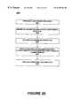
- FIG. 20is a flow chart of a process 2000 performed by one embodiment of the present invention, IOSim 100 .
- Process 2000is implemented in a computer system of FIG. 1 B.
- Process 2000enables a user to conveniently and efficiently create simulation tool input files. A user is relieved of many mundane, convoluted and error prone manual data entry tasks by process 2000 in the creation of simulation tool input files.
- Process 2000also permits a user to easily modify simulation tool input files for convenient analysis of circuits by simulation tools.
- a userutilizes point and click features of a user interface included in IOSim 100 to indicate whether a bus is coupled to an IO buffer circuits and process 2000 automatically modifies corresponding text in a simulation tool input files.
- IOSim 100provides a user friendly interface that enables a user to conveniently and efficiently enter information. For example, presenting information in a GUI with point and click features.
- the user friendly interfacecapable of communicating in a batch mode text format.
- IOSim 100assembles information identified in a user friendly interface. IOSim 100 retrieves files identified in said user friendly interface and searches their contents to analyze what information is included and what additional information is required to create a simulation tool input file. Then missing information required to create a simulation tool input file is gathered by performing iterative exchanges of information between an IOSim, a user and other sources such as library folders. When the requisite information is gathered, electrical characteristic values are inserted in appropriate data entry boxes.
- Step 2003comprises interpretation of information provided in the iterative exchanges in step 2002 .
- Step 2003comprises searching for information in files identified in the user friendly interface and processing retrieved information to determine if any additional data is required to create a simulation tool input file.
- IOSimalso deciphers user initiated information modifications provided via said a user friendly interface.
- IOSim 100inserts information regarding electrical characteristic values in appropriate data entry boxes of a user interface. User initiated information modifications and information retrieved from other sources are processed. Corresponding entries in a simulation tool input file are adjusted to reflect said user initiated information modifications.
- Step 2005includes the creation of a simulation tool input file.
- Simulation tool input filesare constructed based upon the interpretation of information provided in iterative exchanges described in step 2003 and retrieved from said other sources.
- IOSim 100generates an electrical simulation tool input file and produces an electrical characteristic simulation tool input file.
- the electrical simulation tool input filesare compatible with a SPICE simulation tool input file format and a electrical characteristic simulation tool input file is compatible with an IBIS simulation tool input file format.
- the present inventionrelieves a user of tedious tasks associated with creating simulation tool input files. For example, utilizing user friendly GUIs of IOSim 100 a user enters a few library folder names and a relatively simple floor plan file. IOSim 100 retrieves appropriate data and populates entries in subwindows of IOSim 100 . Users can conveniently modify the entries in subwindows they wish. After any modifications to subwindow entries, IOSim 100 automatically creates extensive simulation tool input files such as a SPICE input file and an IBIS simulation file. The electrical component description simulation and the electrical characteristic simulation can be created simultaneously by providing the input files to both electric simulation and electrical characteristic simulation tools at the same time
- IOSim 100will automatically assemble a new simulation tool input file with appropriate modifications. For example, IOSim makes it relatively easy to analyze the impact of cutting a particular bus (e.g., VSS) in between two IO buffer circuits. A user would simply indicate a bus disconnection by clicking on an appropriate right connection indicator or left connection indicator (similar to the example illustrated in FIG. 11 ). IOSim would automatically formulate the appropriate changes to a simulation tool input file to indicate that an IO buffer circuit was no longer connected to a corresponding bus node and it would also automatically adjust bus internal resistance and bus internal inductance to account for the cut.
- VSSbus that is a particular bus
- IOSimwould automatically formulate the appropriate changes to a simulation tool input file to indicate that an IO buffer circuit was no longer connected to a corresponding bus node and it would also automatically adjust bus internal resistance and bus internal inductance to account for the cut.
- IOSimis so convenient to use that in addition to IOSim 100 making it relatively easy for a user to determine the affects of cutting a particular bus in a particular location, a user can easily determine the consequences of cutting a location on a wrong bus or making a cut in the wrong location on the correct bus by simply disconnecting the corresponding left connection indicator and/or right connection indicator.
- the present inventionfacilitates easy rearrangement of a floorplan, including adding, subtracting or repositioning power and ground pads and change IO buffers to compare performance levels.
- the system and method of the present inventionpermits a designer to efficiently and effectively create and modify electrical circuit simulation tool input files.
- the system and methodenables a user to conveniently (enter convey communicate) information sufficient to adequately describe features of the circuit being designed or analyzed while minimizing the amount of data a user has to manually enter.
- the system and methodallow a user to easily modify design features without manually modifying the entire simulation input file.
- the system and method of the present inventionprovide simulation input files including electrical component description simulation tool input files and electrical component description simulation input files such as SPICE formatted input files and IBIS formatted input files. These simulation input files permit detailed signal integrity analysis and characterization of internal and external signals in one simulation session.
- the system and methodeconomically generate simulation input files of a chip's interface circuitry in a manner that allows the use of simulation tools to design and analyze an IO buffer circuit ring integrated on an electronic chip.
Landscapes
- Engineering & Computer Science (AREA)
- Computer Hardware Design (AREA)
- Physics & Mathematics (AREA)
- Theoretical Computer Science (AREA)
- Microelectronics & Electronic Packaging (AREA)
- Evolutionary Computation (AREA)
- Geometry (AREA)
- General Engineering & Computer Science (AREA)
- General Physics & Mathematics (AREA)
- Design And Manufacture Of Integrated Circuits (AREA)
Abstract
Description
Claims (13)
Priority Applications (1)
| Application Number | Priority Date | Filing Date | Title |
|---|---|---|---|
| US09/216,385US6292766B1 (en) | 1998-12-18 | 1998-12-18 | Simulation tool input file generator for interface circuitry |
Applications Claiming Priority (1)
| Application Number | Priority Date | Filing Date | Title |
|---|---|---|---|
| US09/216,385US6292766B1 (en) | 1998-12-18 | 1998-12-18 | Simulation tool input file generator for interface circuitry |
Publications (1)
| Publication Number | Publication Date |
|---|---|
| US6292766B1true US6292766B1 (en) | 2001-09-18 |
Family
ID=22806853
Family Applications (1)
| Application Number | Title | Priority Date | Filing Date |
|---|---|---|---|
| US09/216,385Expired - LifetimeUS6292766B1 (en) | 1998-12-18 | 1998-12-18 | Simulation tool input file generator for interface circuitry |
Country Status (1)
| Country | Link |
|---|---|
| US (1) | US6292766B1 (en) |
Cited By (120)
| Publication number | Priority date | Publication date | Assignee | Title |
|---|---|---|---|---|
| US20020035517A1 (en)* | 2000-09-18 | 2002-03-21 | Seiya Kitagaw | Method of selecting type of electronic part and electronic parts maker server |
| US20020052691A1 (en)* | 2000-08-30 | 2002-05-02 | Hiroshi Yoshida | Server apparatus, transit control method, and computer-readable recording medium storing transit control program |
| US6530065B1 (en)* | 2000-03-14 | 2003-03-04 | Transim Technology Corporation | Client-server simulator, such as an electrical circuit simulator provided by a web server over the internet |
| US20030160826A1 (en)* | 2002-02-26 | 2003-08-28 | Sun Microsystems, Inc. | Method, apparatus and computer product to organize data on a display and facilitate testing of an integrated circuit design |
| US20030182640A1 (en)* | 2002-03-20 | 2003-09-25 | Alani Alaa F. | Signal integrity analysis system |
| US6662352B2 (en)* | 2001-09-06 | 2003-12-09 | International Business Machines Corporation | Method of assigning chip I/O's to package channels |
| US20040002829A1 (en)* | 2002-06-28 | 2004-01-01 | Agilent Technologies, Inc. And Sandia Technologies, Inc. | Semiconductor test data analysis system |
| US20040031001A1 (en)* | 2000-09-14 | 2004-02-12 | Xisheng Zhang | MOSFET modeling for IC design accurate for high frequencies |
| US20040083826A1 (en)* | 2002-08-13 | 2004-05-06 | Csir | Gas borne substance sampling device |
| US6829571B1 (en)* | 2000-06-15 | 2004-12-07 | Hewlett-Packard Development Company, L.P. | Method of determining DC margin of a latch |
| US20040254775A1 (en)* | 2003-06-13 | 2004-12-16 | Arpad Muranyi | Method and apparatus to characterize an electronic device |
| US20050197807A1 (en)* | 2004-03-04 | 2005-09-08 | Jerimy Nelson | System and method for maintaining homogeneity between a model in a computer-aided modeling system and corresponding model documentation |
| US20050222834A1 (en)* | 2002-05-01 | 2005-10-06 | Jackie Riley | Simulation model generation |
| US20050234699A1 (en)* | 2002-12-04 | 2005-10-20 | John Morrison | Data processing system |
| US20060123369A1 (en)* | 2004-12-03 | 2006-06-08 | Lsi Logic Corporation | Ramptime propagation on designs with cycles |
| US7093211B1 (en)* | 2003-11-03 | 2006-08-15 | General Electric Company | Techniques for modeling current spreading uniformity in light emitting diodes |
| US20060224374A1 (en)* | 2005-03-31 | 2006-10-05 | Won Ok Kwon | Method for converting IBIS model to spice behavioral model by extracting resistor and capacitor |
| US7277825B1 (en)* | 2003-04-25 | 2007-10-02 | Unisys Corporation | Apparatus and method for analyzing performance of a data processing system |
| US20080040081A1 (en)* | 2006-02-17 | 2008-02-14 | Elpida Memory, Inc. | Simulation method for improving freedom of setting parameters relating to input/output characteristics of a memory chip |
| US20080059142A1 (en)* | 2006-08-31 | 2008-03-06 | Chlipala James D | Input/Output Buffer Information Specification (IBIS) Model Generation for Multi-chip Modules (MCM) and Similar Devices |
| US20080244484A1 (en)* | 2007-03-28 | 2008-10-02 | Masahito Kumazaki | Circuit design verification system, method and medium |
| US20090037160A1 (en)* | 2007-07-31 | 2009-02-05 | Dix Christopher W | Method and apparatus to serve ibis data |
| US20090172613A1 (en)* | 2003-10-21 | 2009-07-02 | Roberto Suaya | Mutual Inductance extraction using dipole approximations |
| US20100031207A1 (en)* | 2008-07-29 | 2010-02-04 | Fujitsu Limited | Analyzing apparatus and analyzing method |
| US20100064763A1 (en)* | 2008-02-14 | 2010-03-18 | Gaikwad Sangram K | Web-based system and method for configuring test equipment |
| US7835896B1 (en) | 1998-04-06 | 2010-11-16 | Rode Consulting, Inc. | Apparatus for evaluating and demonstrating electronic circuits and components |
| US20120191437A1 (en)* | 2011-01-20 | 2012-07-26 | Elpida Memory, Inc. | Method for extracting ibis simulation model |
| US20120204139A1 (en)* | 2003-10-21 | 2012-08-09 | Mentor Graphics Corporation | Determining mutual inductance between intentional inductors |
| US8560294B1 (en)* | 2008-02-20 | 2013-10-15 | Xilinx, Inc. | Method and apparatus for an automated input/output buffer information specification model generator |
| US8595669B1 (en)* | 2007-08-31 | 2013-11-26 | Cadence Design Systems, Inc. | Flexible noise and delay modeling of circuit stages for static timing analysis of integrated circuit designs |
| US8732648B2 (en) | 2008-03-08 | 2014-05-20 | Mentor Graphics Corporation | High-frequency VLSI interconnect and intentional inductor impedance extraction in the presence of a multi-layer conductive substrate |
| US20160140271A1 (en)* | 2014-11-17 | 2016-05-19 | Taiwan Semiconductor Manufacturing Company, Ltd. | Integrated circuit modeling method |
| US20160274759A1 (en) | 2008-08-25 | 2016-09-22 | Paul J. Dawes | Security system with networked touchscreen and gateway |
| US10051078B2 (en) | 2007-06-12 | 2018-08-14 | Icontrol Networks, Inc. | WiFi-to-serial encapsulation in systems |
| US10062245B2 (en) | 2005-03-16 | 2018-08-28 | Icontrol Networks, Inc. | Cross-client sensor user interface in an integrated security network |
| US10062273B2 (en) | 2010-09-28 | 2018-08-28 | Icontrol Networks, Inc. | Integrated security system with parallel processing architecture |
| US10078958B2 (en) | 2010-12-17 | 2018-09-18 | Icontrol Networks, Inc. | Method and system for logging security event data |
| US10079839B1 (en) | 2007-06-12 | 2018-09-18 | Icontrol Networks, Inc. | Activation of gateway device |
| US10091014B2 (en) | 2005-03-16 | 2018-10-02 | Icontrol Networks, Inc. | Integrated security network with security alarm signaling system |
| US10127801B2 (en) | 2005-03-16 | 2018-11-13 | Icontrol Networks, Inc. | Integrated security system with parallel processing architecture |
| US10142166B2 (en) | 2004-03-16 | 2018-11-27 | Icontrol Networks, Inc. | Takeover of security network |
| US10140840B2 (en) | 2007-04-23 | 2018-11-27 | Icontrol Networks, Inc. | Method and system for providing alternate network access |
| US10142394B2 (en) | 2007-06-12 | 2018-11-27 | Icontrol Networks, Inc. | Generating risk profile using data of home monitoring and security system |
| US10142392B2 (en) | 2007-01-24 | 2018-11-27 | Icontrol Networks, Inc. | Methods and systems for improved system performance |
| US10156831B2 (en) | 2004-03-16 | 2018-12-18 | Icontrol Networks, Inc. | Automation system with mobile interface |
| US10200504B2 (en) | 2007-06-12 | 2019-02-05 | Icontrol Networks, Inc. | Communication protocols over internet protocol (IP) networks |
| US10237237B2 (en) | 2007-06-12 | 2019-03-19 | Icontrol Networks, Inc. | Communication protocols in integrated systems |
| US10237806B2 (en) | 2009-04-30 | 2019-03-19 | Icontrol Networks, Inc. | Activation of a home automation controller |
| US10313303B2 (en) | 2007-06-12 | 2019-06-04 | Icontrol Networks, Inc. | Forming a security network including integrated security system components and network devices |
| US10339791B2 (en) | 2007-06-12 | 2019-07-02 | Icontrol Networks, Inc. | Security network integrated with premise security system |
| US10348575B2 (en) | 2013-06-27 | 2019-07-09 | Icontrol Networks, Inc. | Control system user interface |
| US10365810B2 (en) | 2007-06-12 | 2019-07-30 | Icontrol Networks, Inc. | Control system user interface |
| US10382452B1 (en) | 2007-06-12 | 2019-08-13 | Icontrol Networks, Inc. | Communication protocols in integrated systems |
| US10380871B2 (en) | 2005-03-16 | 2019-08-13 | Icontrol Networks, Inc. | Control system user interface |
| US10389736B2 (en) | 2007-06-12 | 2019-08-20 | Icontrol Networks, Inc. | Communication protocols in integrated systems |
| US10423309B2 (en) | 2007-06-12 | 2019-09-24 | Icontrol Networks, Inc. | Device integration framework |
| US10498830B2 (en) | 2007-06-12 | 2019-12-03 | Icontrol Networks, Inc. | Wi-Fi-to-serial encapsulation in systems |
| US10522026B2 (en) | 2008-08-11 | 2019-12-31 | Icontrol Networks, Inc. | Automation system user interface with three-dimensional display |
| US10523689B2 (en) | 2007-06-12 | 2019-12-31 | Icontrol Networks, Inc. | Communication protocols over internet protocol (IP) networks |
| US10530839B2 (en) | 2008-08-11 | 2020-01-07 | Icontrol Networks, Inc. | Integrated cloud system with lightweight gateway for premises automation |
| US10559193B2 (en) | 2002-02-01 | 2020-02-11 | Comcast Cable Communications, Llc | Premises management systems |
| US10616075B2 (en) | 2007-06-12 | 2020-04-07 | Icontrol Networks, Inc. | Communication protocols in integrated systems |
| US10666523B2 (en) | 2007-06-12 | 2020-05-26 | Icontrol Networks, Inc. | Communication protocols in integrated systems |
| US10691295B2 (en) | 2004-03-16 | 2020-06-23 | Icontrol Networks, Inc. | User interface in a premises network |
| US10721087B2 (en) | 2005-03-16 | 2020-07-21 | Icontrol Networks, Inc. | Method for networked touchscreen with integrated interfaces |
| US10747216B2 (en) | 2007-02-28 | 2020-08-18 | Icontrol Networks, Inc. | Method and system for communicating with and controlling an alarm system from a remote server |
| US10785319B2 (en) | 2006-06-12 | 2020-09-22 | Icontrol Networks, Inc. | IP device discovery systems and methods |
| US10841381B2 (en) | 2005-03-16 | 2020-11-17 | Icontrol Networks, Inc. | Security system with networked touchscreen |
| US10979389B2 (en) | 2004-03-16 | 2021-04-13 | Icontrol Networks, Inc. | Premises management configuration and control |
| US10999254B2 (en) | 2005-03-16 | 2021-05-04 | Icontrol Networks, Inc. | System for data routing in networks |
| US11089122B2 (en) | 2007-06-12 | 2021-08-10 | Icontrol Networks, Inc. | Controlling data routing among networks |
| US11113950B2 (en) | 2005-03-16 | 2021-09-07 | Icontrol Networks, Inc. | Gateway integrated with premises security system |
| US11146637B2 (en) | 2014-03-03 | 2021-10-12 | Icontrol Networks, Inc. | Media content management |
| US11144699B2 (en)* | 2020-02-25 | 2021-10-12 | Samsung Electronics Co., Ltd. | Method implemented on computer system executing instructions for semiconductor design simulation |
| US11153266B2 (en) | 2004-03-16 | 2021-10-19 | Icontrol Networks, Inc. | Gateway registry methods and systems |
| US11182060B2 (en) | 2004-03-16 | 2021-11-23 | Icontrol Networks, Inc. | Networked touchscreen with integrated interfaces |
| US11201755B2 (en) | 2004-03-16 | 2021-12-14 | Icontrol Networks, Inc. | Premises system management using status signal |
| US11212192B2 (en) | 2007-06-12 | 2021-12-28 | Icontrol Networks, Inc. | Communication protocols in integrated systems |
| US11218878B2 (en) | 2007-06-12 | 2022-01-04 | Icontrol Networks, Inc. | Communication protocols in integrated systems |
| US11237714B2 (en) | 2007-06-12 | 2022-02-01 | Control Networks, Inc. | Control system user interface |
| US11240059B2 (en) | 2010-12-20 | 2022-02-01 | Icontrol Networks, Inc. | Defining and implementing sensor triggered response rules |
| US11244545B2 (en) | 2004-03-16 | 2022-02-08 | Icontrol Networks, Inc. | Cross-client sensor user interface in an integrated security network |
| US11258625B2 (en) | 2008-08-11 | 2022-02-22 | Icontrol Networks, Inc. | Mobile premises automation platform |
| US11277465B2 (en) | 2004-03-16 | 2022-03-15 | Icontrol Networks, Inc. | Generating risk profile using data of home monitoring and security system |
| US11310199B2 (en) | 2004-03-16 | 2022-04-19 | Icontrol Networks, Inc. | Premises management configuration and control |
| US11316753B2 (en) | 2007-06-12 | 2022-04-26 | Icontrol Networks, Inc. | Communication protocols in integrated systems |
| US11316958B2 (en) | 2008-08-11 | 2022-04-26 | Icontrol Networks, Inc. | Virtual device systems and methods |
| US11343380B2 (en) | 2004-03-16 | 2022-05-24 | Icontrol Networks, Inc. | Premises system automation |
| US11368327B2 (en) | 2008-08-11 | 2022-06-21 | Icontrol Networks, Inc. | Integrated cloud system for premises automation |
| US11398147B2 (en) | 2010-09-28 | 2022-07-26 | Icontrol Networks, Inc. | Method, system and apparatus for automated reporting of account and sensor zone information to a central station |
| US11405463B2 (en) | 2014-03-03 | 2022-08-02 | Icontrol Networks, Inc. | Media content management |
| US11424980B2 (en) | 2005-03-16 | 2022-08-23 | Icontrol Networks, Inc. | Forming a security network including integrated security system components |
| US11423756B2 (en) | 2007-06-12 | 2022-08-23 | Icontrol Networks, Inc. | Communication protocols in integrated systems |
| US11451409B2 (en) | 2005-03-16 | 2022-09-20 | Icontrol Networks, Inc. | Security network integrating security system and network devices |
| US11489812B2 (en) | 2004-03-16 | 2022-11-01 | Icontrol Networks, Inc. | Forming a security network including integrated security system components and network devices |
| US11496568B2 (en) | 2005-03-16 | 2022-11-08 | Icontrol Networks, Inc. | Security system with networked touchscreen |
| US11582065B2 (en) | 2007-06-12 | 2023-02-14 | Icontrol Networks, Inc. | Systems and methods for device communication |
| US11601810B2 (en) | 2007-06-12 | 2023-03-07 | Icontrol Networks, Inc. | Communication protocols in integrated systems |
| US11615697B2 (en) | 2005-03-16 | 2023-03-28 | Icontrol Networks, Inc. | Premise management systems and methods |
| US11646907B2 (en) | 2007-06-12 | 2023-05-09 | Icontrol Networks, Inc. | Communication protocols in integrated systems |
| US11677577B2 (en) | 2004-03-16 | 2023-06-13 | Icontrol Networks, Inc. | Premises system management using status signal |
| CN116306441A (en)* | 2023-03-10 | 2023-06-23 | 西安电子科技大学 | Digital integrated circuit radiation effect model construction method based on measurement system |
| US11700142B2 (en) | 2005-03-16 | 2023-07-11 | Icontrol Networks, Inc. | Security network integrating security system and network devices |
| US11706045B2 (en) | 2005-03-16 | 2023-07-18 | Icontrol Networks, Inc. | Modular electronic display platform |
| US11706279B2 (en) | 2007-01-24 | 2023-07-18 | Icontrol Networks, Inc. | Methods and systems for data communication |
| US11729255B2 (en) | 2008-08-11 | 2023-08-15 | Icontrol Networks, Inc. | Integrated cloud system with lightweight gateway for premises automation |
| US11750414B2 (en) | 2010-12-16 | 2023-09-05 | Icontrol Networks, Inc. | Bidirectional security sensor communication for a premises security system |
| US11758026B2 (en) | 2008-08-11 | 2023-09-12 | Icontrol Networks, Inc. | Virtual device systems and methods |
| US11792330B2 (en) | 2005-03-16 | 2023-10-17 | Icontrol Networks, Inc. | Communication and automation in a premises management system |
| US11792036B2 (en) | 2008-08-11 | 2023-10-17 | Icontrol Networks, Inc. | Mobile premises automation platform |
| US11811845B2 (en) | 2004-03-16 | 2023-11-07 | Icontrol Networks, Inc. | Communication protocols over internet protocol (IP) networks |
| US11816323B2 (en) | 2008-06-25 | 2023-11-14 | Icontrol Networks, Inc. | Automation system user interface |
| US11831462B2 (en) | 2007-08-24 | 2023-11-28 | Icontrol Networks, Inc. | Controlling data routing in premises management systems |
| US11916870B2 (en) | 2004-03-16 | 2024-02-27 | Icontrol Networks, Inc. | Gateway registry methods and systems |
| US11916928B2 (en) | 2008-01-24 | 2024-02-27 | Icontrol Networks, Inc. | Communication protocols over internet protocol (IP) networks |
| US12003387B2 (en) | 2012-06-27 | 2024-06-04 | Comcast Cable Communications, Llc | Control system user interface |
| US12063220B2 (en) | 2004-03-16 | 2024-08-13 | Icontrol Networks, Inc. | Communication protocols in integrated systems |
| US12063221B2 (en) | 2006-06-12 | 2024-08-13 | Icontrol Networks, Inc. | Activation of gateway device |
| US12184443B2 (en) | 2007-06-12 | 2024-12-31 | Icontrol Networks, Inc. | Controlling data routing among networks |
| US12283172B2 (en) | 2007-06-12 | 2025-04-22 | Icontrol Networks, Inc. | Communication protocols in integrated systems |
Citations (5)
| Publication number | Priority date | Publication date | Assignee | Title |
|---|---|---|---|---|
| US5278770A (en)* | 1990-06-25 | 1994-01-11 | Brooklin J. Gore | Method for generating input data for an electronic circuit simulator |
| US5699264A (en)* | 1995-12-12 | 1997-12-16 | Mitsubishi Electric Semiconductor Software Co., Ltd. | Semiconductor circuit design verifying apparatus |
| US5781760A (en)* | 1995-11-16 | 1998-07-14 | Motorola, Inc. | Methods of simulating an electronic circuit design and forming an integrated circuit |
| US5790436A (en)* | 1995-04-28 | 1998-08-04 | Bta Technology, Inc. | Realistic worst-case circuit simulation system and method |
| US5933356A (en)* | 1990-04-06 | 1999-08-03 | Lsi Logic Corporation | Method and system for creating and verifying structural logic model of electronic design from behavioral description, including generation of logic and timing models |
- 1998
- 1998-12-18USUS09/216,385patent/US6292766B1/ennot_activeExpired - Lifetime
Patent Citations (5)
| Publication number | Priority date | Publication date | Assignee | Title |
|---|---|---|---|---|
| US5933356A (en)* | 1990-04-06 | 1999-08-03 | Lsi Logic Corporation | Method and system for creating and verifying structural logic model of electronic design from behavioral description, including generation of logic and timing models |
| US5278770A (en)* | 1990-06-25 | 1994-01-11 | Brooklin J. Gore | Method for generating input data for an electronic circuit simulator |
| US5790436A (en)* | 1995-04-28 | 1998-08-04 | Bta Technology, Inc. | Realistic worst-case circuit simulation system and method |
| US5781760A (en)* | 1995-11-16 | 1998-07-14 | Motorola, Inc. | Methods of simulating an electronic circuit design and forming an integrated circuit |
| US5699264A (en)* | 1995-12-12 | 1997-12-16 | Mitsubishi Electric Semiconductor Software Co., Ltd. | Semiconductor circuit design verifying apparatus |
Non-Patent Citations (5)
| Title |
|---|
| Cuny, R. H. G., "SPICE and IBIS Modeling Kits the Basis for Signal Integration Analyses", IEEE Intern. Symp. on Electromagnetic Compatibility, pp. 204-208, Aug. 1996.* |
| Li et al. "Automated Extraction of Parasitic BJTs from CMOS I/O Circuits Under ESD Stress", International Integrated Reliability Workshop Final Report, pp. 103-109, Oct. 1997.* |
| Shi et al., "Simulation and Measurement for Decoupling on Multilayer DC Power Buses", IEEE 1996 International Symposium on Electromagnetic Compatibility, pp. 430-435, Aug. 1996.* |
| Tehrani et al., "Extraction of Transient Behavioral Model of Digital I/O Buffers from IBIS", Proceedings of the 46th Electronic Components and Tech. Conf., pp. 1009-1015, May 1996.* |
| Ying et al., "The Development of Analog SPICE Behavioral Model Based on IBIS Model", Proceedings Ninth Great Lakes Symp. on VLSI, pp. 101-104, Mar. 1999.* |
Cited By (238)
| Publication number | Priority date | Publication date | Assignee | Title |
|---|---|---|---|---|
| US7835896B1 (en) | 1998-04-06 | 2010-11-16 | Rode Consulting, Inc. | Apparatus for evaluating and demonstrating electronic circuits and components |
| US6530065B1 (en)* | 2000-03-14 | 2003-03-04 | Transim Technology Corporation | Client-server simulator, such as an electrical circuit simulator provided by a web server over the internet |
| US6829571B1 (en)* | 2000-06-15 | 2004-12-07 | Hewlett-Packard Development Company, L.P. | Method of determining DC margin of a latch |
| US20020052691A1 (en)* | 2000-08-30 | 2002-05-02 | Hiroshi Yoshida | Server apparatus, transit control method, and computer-readable recording medium storing transit control program |
| US7216097B2 (en)* | 2000-08-30 | 2007-05-08 | Fujitsu Limited | Server apparatus, transit control method, and computer-readable recording medium storing transit control program |
| US6851097B2 (en)* | 2000-09-14 | 2005-02-01 | Cadence Design Systems, Inc. | MOSFET modeling for IC design accurate for high frequencies |
| US20080109204A1 (en)* | 2000-09-14 | 2008-05-08 | Xisheng Zhang | MOSFET Modeling for IC Design Accurate for High Frequencies |
| US20050114111A1 (en)* | 2000-09-14 | 2005-05-26 | Xisheng Zhang | MOSFET modeling for IC design accurate for high frequencies |
| US7313770B2 (en) | 2000-09-14 | 2007-12-25 | Cadence Design Systems, Inc. | MOSFET modeling for IC design accurate for high frequencies |
| US20040031001A1 (en)* | 2000-09-14 | 2004-02-12 | Xisheng Zhang | MOSFET modeling for IC design accurate for high frequencies |
| US7735033B2 (en) | 2000-09-14 | 2010-06-08 | Cadence Design Systems, Inc. | MOSFET modeling for IC design accurate for high frequencies |
| US7899896B2 (en) | 2000-09-18 | 2011-03-01 | Sanyo Electric Co., Ltd. | Method of selecting type of electronic part and electronic parts maker server |
| US20020035517A1 (en)* | 2000-09-18 | 2002-03-21 | Seiya Kitagaw | Method of selecting type of electronic part and electronic parts maker server |
| US7386811B2 (en)* | 2000-09-18 | 2008-06-10 | Sanyo Electric Co., Ltd. | Method of selecting type of electronic part and electronic parts maker server |
| US20080033837A1 (en)* | 2000-09-18 | 2008-02-07 | Sanyo Electric Co., Ltd. | Method of selecting type of electronic part and electronic parts maker server |
| US6662352B2 (en)* | 2001-09-06 | 2003-12-09 | International Business Machines Corporation | Method of assigning chip I/O's to package channels |
| US10559193B2 (en) | 2002-02-01 | 2020-02-11 | Comcast Cable Communications, Llc | Premises management systems |
| US20030160826A1 (en)* | 2002-02-26 | 2003-08-28 | Sun Microsystems, Inc. | Method, apparatus and computer product to organize data on a display and facilitate testing of an integrated circuit design |
| US20030182640A1 (en)* | 2002-03-20 | 2003-09-25 | Alani Alaa F. | Signal integrity analysis system |
| US20050222834A1 (en)* | 2002-05-01 | 2005-10-06 | Jackie Riley | Simulation model generation |
| US6898545B2 (en)* | 2002-06-28 | 2005-05-24 | Agilent Technologies Inc | Semiconductor test data analysis system |
| US7035752B2 (en) | 2002-06-28 | 2006-04-25 | Agilent Technologies, Inc. | Semiconductor test data analysis system |
| US20050119852A1 (en)* | 2002-06-28 | 2005-06-02 | Agilent Technologies, Inc. | Semiconductor test data analysis system |
| US20040002829A1 (en)* | 2002-06-28 | 2004-01-01 | Agilent Technologies, Inc. And Sandia Technologies, Inc. | Semiconductor test data analysis system |
| US20040083826A1 (en)* | 2002-08-13 | 2004-05-06 | Csir | Gas borne substance sampling device |
| US20050234699A1 (en)* | 2002-12-04 | 2005-10-20 | John Morrison | Data processing system |
| US7277825B1 (en)* | 2003-04-25 | 2007-10-02 | Unisys Corporation | Apparatus and method for analyzing performance of a data processing system |
| US20040254775A1 (en)* | 2003-06-13 | 2004-12-16 | Arpad Muranyi | Method and apparatus to characterize an electronic device |
| US8650522B2 (en)* | 2003-10-21 | 2014-02-11 | Mentor Graphics Corporation | Determining mutual inductance between intentional inductors |
| US8826204B2 (en) | 2003-10-21 | 2014-09-02 | Mentor Graphics Corporation | Mutual inductance extraction using dipole approximations |
| US8549449B2 (en) | 2003-10-21 | 2013-10-01 | Mentor Graphics Corporation | Mutual inductance extraction using dipole approximations |
| US20120204139A1 (en)* | 2003-10-21 | 2012-08-09 | Mentor Graphics Corporation | Determining mutual inductance between intentional inductors |
| US20090172613A1 (en)* | 2003-10-21 | 2009-07-02 | Roberto Suaya | Mutual Inductance extraction using dipole approximations |
| US7093211B1 (en)* | 2003-11-03 | 2006-08-15 | General Electric Company | Techniques for modeling current spreading uniformity in light emitting diodes |
| US20050197807A1 (en)* | 2004-03-04 | 2005-09-08 | Jerimy Nelson | System and method for maintaining homogeneity between a model in a computer-aided modeling system and corresponding model documentation |
| US11757834B2 (en) | 2004-03-16 | 2023-09-12 | Icontrol Networks, Inc. | Communication protocols in integrated systems |
| US11343380B2 (en) | 2004-03-16 | 2022-05-24 | Icontrol Networks, Inc. | Premises system automation |
| US11810445B2 (en) | 2004-03-16 | 2023-11-07 | Icontrol Networks, Inc. | Cross-client sensor user interface in an integrated security network |
| US11782394B2 (en) | 2004-03-16 | 2023-10-10 | Icontrol Networks, Inc. | Automation system with mobile interface |
| US11811845B2 (en) | 2004-03-16 | 2023-11-07 | Icontrol Networks, Inc. | Communication protocols over internet protocol (IP) networks |
| US11893874B2 (en) | 2004-03-16 | 2024-02-06 | Icontrol Networks, Inc. | Networked touchscreen with integrated interfaces |
| US11916870B2 (en) | 2004-03-16 | 2024-02-27 | Icontrol Networks, Inc. | Gateway registry methods and systems |
| US10447491B2 (en) | 2004-03-16 | 2019-10-15 | Icontrol Networks, Inc. | Premises system management using status signal |
| US11677577B2 (en) | 2004-03-16 | 2023-06-13 | Icontrol Networks, Inc. | Premises system management using status signal |
| US11991306B2 (en) | 2004-03-16 | 2024-05-21 | Icontrol Networks, Inc. | Premises system automation |
| US11656667B2 (en) | 2004-03-16 | 2023-05-23 | Icontrol Networks, Inc. | Integrated security system with parallel processing architecture |
| US12063220B2 (en) | 2004-03-16 | 2024-08-13 | Icontrol Networks, Inc. | Communication protocols in integrated systems |
| US11626006B2 (en) | 2004-03-16 | 2023-04-11 | Icontrol Networks, Inc. | Management of a security system at a premises |
| US11625008B2 (en) | 2004-03-16 | 2023-04-11 | Icontrol Networks, Inc. | Premises management networking |
| US10691295B2 (en) | 2004-03-16 | 2020-06-23 | Icontrol Networks, Inc. | User interface in a premises network |
| US10692356B2 (en) | 2004-03-16 | 2020-06-23 | Icontrol Networks, Inc. | Control system user interface |
| US11601397B2 (en) | 2004-03-16 | 2023-03-07 | Icontrol Networks, Inc. | Premises management configuration and control |
| US12253833B2 (en) | 2004-03-16 | 2025-03-18 | Icontrol Networks, Inc. | Automation system with mobile interface |
| US11588787B2 (en) | 2004-03-16 | 2023-02-21 | Icontrol Networks, Inc. | Premises management configuration and control |
| US11537186B2 (en) | 2004-03-16 | 2022-12-27 | Icontrol Networks, Inc. | Integrated security system with parallel processing architecture |
| US11489812B2 (en) | 2004-03-16 | 2022-11-01 | Icontrol Networks, Inc. | Forming a security network including integrated security system components and network devices |
| US11449012B2 (en) | 2004-03-16 | 2022-09-20 | Icontrol Networks, Inc. | Premises management networking |
| US11410531B2 (en) | 2004-03-16 | 2022-08-09 | Icontrol Networks, Inc. | Automation system user interface with three-dimensional display |
| US11378922B2 (en) | 2004-03-16 | 2022-07-05 | Icontrol Networks, Inc. | Automation system with mobile interface |
| US11368429B2 (en) | 2004-03-16 | 2022-06-21 | Icontrol Networks, Inc. | Premises management configuration and control |
| US10735249B2 (en) | 2004-03-16 | 2020-08-04 | Icontrol Networks, Inc. | Management of a security system at a premises |
| US11310199B2 (en) | 2004-03-16 | 2022-04-19 | Icontrol Networks, Inc. | Premises management configuration and control |
| US11277465B2 (en) | 2004-03-16 | 2022-03-15 | Icontrol Networks, Inc. | Generating risk profile using data of home monitoring and security system |
| US11244545B2 (en) | 2004-03-16 | 2022-02-08 | Icontrol Networks, Inc. | Cross-client sensor user interface in an integrated security network |
| US11201755B2 (en) | 2004-03-16 | 2021-12-14 | Icontrol Networks, Inc. | Premises system management using status signal |
| US11184322B2 (en) | 2004-03-16 | 2021-11-23 | Icontrol Networks, Inc. | Communication protocols in integrated systems |
| US11182060B2 (en) | 2004-03-16 | 2021-11-23 | Icontrol Networks, Inc. | Networked touchscreen with integrated interfaces |
| US10142166B2 (en) | 2004-03-16 | 2018-11-27 | Icontrol Networks, Inc. | Takeover of security network |
| US11175793B2 (en) | 2004-03-16 | 2021-11-16 | Icontrol Networks, Inc. | User interface in a premises network |
| US11159484B2 (en) | 2004-03-16 | 2021-10-26 | Icontrol Networks, Inc. | Forming a security network including integrated security system components and network devices |
| US11153266B2 (en) | 2004-03-16 | 2021-10-19 | Icontrol Networks, Inc. | Gateway registry methods and systems |
| US10156831B2 (en) | 2004-03-16 | 2018-12-18 | Icontrol Networks, Inc. | Automation system with mobile interface |
| US11082395B2 (en) | 2004-03-16 | 2021-08-03 | Icontrol Networks, Inc. | Premises management configuration and control |
| US11043112B2 (en) | 2004-03-16 | 2021-06-22 | Icontrol Networks, Inc. | Integrated security system with parallel processing architecture |
| US11037433B2 (en) | 2004-03-16 | 2021-06-15 | Icontrol Networks, Inc. | Management of a security system at a premises |
| US10992784B2 (en) | 2004-03-16 | 2021-04-27 | Control Networks, Inc. | Communication protocols over internet protocol (IP) networks |
| US10979389B2 (en) | 2004-03-16 | 2021-04-13 | Icontrol Networks, Inc. | Premises management configuration and control |
| US10890881B2 (en) | 2004-03-16 | 2021-01-12 | Icontrol Networks, Inc. | Premises management networking |
| US10796557B2 (en) | 2004-03-16 | 2020-10-06 | Icontrol Networks, Inc. | Automation system user interface with three-dimensional display |
| US10754304B2 (en) | 2004-03-16 | 2020-08-25 | Icontrol Networks, Inc. | Automation system with mobile interface |
| US7568175B2 (en) | 2004-12-03 | 2009-07-28 | Lsi Corporation | Ramptime propagation on designs with cycles |
| US7246336B2 (en) | 2004-12-03 | 2007-07-17 | Lsi Corporation | Ramptime propagation on designs with cycles |
| US20070234255A1 (en)* | 2004-12-03 | 2007-10-04 | Lsi Logic Corporation | Ramptime propagation on designs with cycles |
| US20060123369A1 (en)* | 2004-12-03 | 2006-06-08 | Lsi Logic Corporation | Ramptime propagation on designs with cycles |
| US11615697B2 (en) | 2005-03-16 | 2023-03-28 | Icontrol Networks, Inc. | Premise management systems and methods |
| US10091014B2 (en) | 2005-03-16 | 2018-10-02 | Icontrol Networks, Inc. | Integrated security network with security alarm signaling system |
| US11595364B2 (en) | 2005-03-16 | 2023-02-28 | Icontrol Networks, Inc. | System for data routing in networks |
| US11496568B2 (en) | 2005-03-16 | 2022-11-08 | Icontrol Networks, Inc. | Security system with networked touchscreen |
| US11451409B2 (en) | 2005-03-16 | 2022-09-20 | Icontrol Networks, Inc. | Security network integrating security system and network devices |
| US11424980B2 (en) | 2005-03-16 | 2022-08-23 | Icontrol Networks, Inc. | Forming a security network including integrated security system components |
| US11113950B2 (en) | 2005-03-16 | 2021-09-07 | Icontrol Networks, Inc. | Gateway integrated with premises security system |
| US10127801B2 (en) | 2005-03-16 | 2018-11-13 | Icontrol Networks, Inc. | Integrated security system with parallel processing architecture |
| US10999254B2 (en) | 2005-03-16 | 2021-05-04 | Icontrol Networks, Inc. | System for data routing in networks |
| US11700142B2 (en) | 2005-03-16 | 2023-07-11 | Icontrol Networks, Inc. | Security network integrating security system and network devices |
| US11367340B2 (en) | 2005-03-16 | 2022-06-21 | Icontrol Networks, Inc. | Premise management systems and methods |
| US10930136B2 (en) | 2005-03-16 | 2021-02-23 | Icontrol Networks, Inc. | Premise management systems and methods |
| US11706045B2 (en) | 2005-03-16 | 2023-07-18 | Icontrol Networks, Inc. | Modular electronic display platform |
| US10841381B2 (en) | 2005-03-16 | 2020-11-17 | Icontrol Networks, Inc. | Security system with networked touchscreen |
| US10062245B2 (en) | 2005-03-16 | 2018-08-28 | Icontrol Networks, Inc. | Cross-client sensor user interface in an integrated security network |
| US12277853B2 (en) | 2005-03-16 | 2025-04-15 | Icontrol Networks, Inc. | Gateway integrated with premises security system |
| US11824675B2 (en) | 2005-03-16 | 2023-11-21 | Icontrol Networks, Inc. | Networked touchscreen with integrated interfaces |
| US11792330B2 (en) | 2005-03-16 | 2023-10-17 | Icontrol Networks, Inc. | Communication and automation in a premises management system |
| US10380871B2 (en) | 2005-03-16 | 2019-08-13 | Icontrol Networks, Inc. | Control system user interface |
| US10721087B2 (en) | 2005-03-16 | 2020-07-21 | Icontrol Networks, Inc. | Method for networked touchscreen with integrated interfaces |
| US7395192B2 (en) | 2005-03-31 | 2008-07-01 | Electronics And Telecommunications Research Institute | Method for converting IBIS model to SPICE behavioral model by extracting resistor and capacitor |
| US20060224374A1 (en)* | 2005-03-31 | 2006-10-05 | Won Ok Kwon | Method for converting IBIS model to spice behavioral model by extracting resistor and capacitor |
| US9129078B1 (en)* | 2005-07-01 | 2015-09-08 | Cadence Design Systems, Inc. | Static timing analysis of integrated circuit designs with flexible noise and delay models of circuit stages |
| US20080040081A1 (en)* | 2006-02-17 | 2008-02-14 | Elpida Memory, Inc. | Simulation method for improving freedom of setting parameters relating to input/output characteristics of a memory chip |
| US10785319B2 (en) | 2006-06-12 | 2020-09-22 | Icontrol Networks, Inc. | IP device discovery systems and methods |
| US11418518B2 (en) | 2006-06-12 | 2022-08-16 | Icontrol Networks, Inc. | Activation of gateway device |
| US12063221B2 (en) | 2006-06-12 | 2024-08-13 | Icontrol Networks, Inc. | Activation of gateway device |
| US10616244B2 (en) | 2006-06-12 | 2020-04-07 | Icontrol Networks, Inc. | Activation of gateway device |
| US8180600B2 (en)* | 2006-08-31 | 2012-05-15 | Agere Systems Inc. | Input/output buffer information specification (IBIS) model generation for multi-chip modules (MCM) and similar devices |
| US20080059142A1 (en)* | 2006-08-31 | 2008-03-06 | Chlipala James D | Input/Output Buffer Information Specification (IBIS) Model Generation for Multi-chip Modules (MCM) and Similar Devices |
| US11706279B2 (en) | 2007-01-24 | 2023-07-18 | Icontrol Networks, Inc. | Methods and systems for data communication |
| US11412027B2 (en) | 2007-01-24 | 2022-08-09 | Icontrol Networks, Inc. | Methods and systems for data communication |
| US10225314B2 (en) | 2007-01-24 | 2019-03-05 | Icontrol Networks, Inc. | Methods and systems for improved system performance |
| US12120171B2 (en) | 2007-01-24 | 2024-10-15 | Icontrol Networks, Inc. | Methods and systems for data communication |
| US11418572B2 (en) | 2007-01-24 | 2022-08-16 | Icontrol Networks, Inc. | Methods and systems for improved system performance |
| US10142392B2 (en) | 2007-01-24 | 2018-11-27 | Icontrol Networks, Inc. | Methods and systems for improved system performance |
| US10657794B1 (en) | 2007-02-28 | 2020-05-19 | Icontrol Networks, Inc. | Security, monitoring and automation controller access and use of legacy security control panel information |
| US11194320B2 (en) | 2007-02-28 | 2021-12-07 | Icontrol Networks, Inc. | Method and system for managing communication connectivity |
| US11809174B2 (en) | 2007-02-28 | 2023-11-07 | Icontrol Networks, Inc. | Method and system for managing communication connectivity |
| US10747216B2 (en) | 2007-02-28 | 2020-08-18 | Icontrol Networks, Inc. | Method and system for communicating with and controlling an alarm system from a remote server |
| US20080244484A1 (en)* | 2007-03-28 | 2008-10-02 | Masahito Kumazaki | Circuit design verification system, method and medium |
| US10140840B2 (en) | 2007-04-23 | 2018-11-27 | Icontrol Networks, Inc. | Method and system for providing alternate network access |
| US11132888B2 (en) | 2007-04-23 | 2021-09-28 | Icontrol Networks, Inc. | Method and system for providing alternate network access |
| US11663902B2 (en) | 2007-04-23 | 2023-05-30 | Icontrol Networks, Inc. | Method and system for providing alternate network access |
| US10672254B2 (en) | 2007-04-23 | 2020-06-02 | Icontrol Networks, Inc. | Method and system for providing alternate network access |
| US11722896B2 (en) | 2007-06-12 | 2023-08-08 | Icontrol Networks, Inc. | Communication protocols in integrated systems |
| US10339791B2 (en) | 2007-06-12 | 2019-07-02 | Icontrol Networks, Inc. | Security network integrated with premise security system |
| US11582065B2 (en) | 2007-06-12 | 2023-02-14 | Icontrol Networks, Inc. | Systems and methods for device communication |
| US10200504B2 (en) | 2007-06-12 | 2019-02-05 | Icontrol Networks, Inc. | Communication protocols over internet protocol (IP) networks |
| US10237237B2 (en) | 2007-06-12 | 2019-03-19 | Icontrol Networks, Inc. | Communication protocols in integrated systems |
| US11212192B2 (en) | 2007-06-12 | 2021-12-28 | Icontrol Networks, Inc. | Communication protocols in integrated systems |
| US11218878B2 (en) | 2007-06-12 | 2022-01-04 | Icontrol Networks, Inc. | Communication protocols in integrated systems |
| US10313303B2 (en) | 2007-06-12 | 2019-06-04 | Icontrol Networks, Inc. | Forming a security network including integrated security system components and network devices |
| US11237714B2 (en) | 2007-06-12 | 2022-02-01 | Control Networks, Inc. | Control system user interface |
| US11601810B2 (en) | 2007-06-12 | 2023-03-07 | Icontrol Networks, Inc. | Communication protocols in integrated systems |
| US10079839B1 (en) | 2007-06-12 | 2018-09-18 | Icontrol Networks, Inc. | Activation of gateway device |
| US10389736B2 (en) | 2007-06-12 | 2019-08-20 | Icontrol Networks, Inc. | Communication protocols in integrated systems |
| US12184443B2 (en) | 2007-06-12 | 2024-12-31 | Icontrol Networks, Inc. | Controlling data routing among networks |
| US12250547B2 (en) | 2007-06-12 | 2025-03-11 | Icontrol Networks, Inc. | Communication protocols in integrated systems |
| US10666523B2 (en) | 2007-06-12 | 2020-05-26 | Icontrol Networks, Inc. | Communication protocols in integrated systems |
| US10365810B2 (en) | 2007-06-12 | 2019-07-30 | Icontrol Networks, Inc. | Control system user interface |
| US11316753B2 (en) | 2007-06-12 | 2022-04-26 | Icontrol Networks, Inc. | Communication protocols in integrated systems |
| US11894986B2 (en) | 2007-06-12 | 2024-02-06 | Icontrol Networks, Inc. | Communication protocols in integrated systems |
| US11089122B2 (en) | 2007-06-12 | 2021-08-10 | Icontrol Networks, Inc. | Controlling data routing among networks |
| US10423309B2 (en) | 2007-06-12 | 2019-09-24 | Icontrol Networks, Inc. | Device integration framework |
| US11646907B2 (en) | 2007-06-12 | 2023-05-09 | Icontrol Networks, Inc. | Communication protocols in integrated systems |
| US10051078B2 (en) | 2007-06-12 | 2018-08-14 | Icontrol Networks, Inc. | WiFi-to-serial encapsulation in systems |
| US12283172B2 (en) | 2007-06-12 | 2025-04-22 | Icontrol Networks, Inc. | Communication protocols in integrated systems |
| US12284057B2 (en) | 2007-06-12 | 2025-04-22 | Icontrol Networks, Inc. | Systems and methods for device communication |
| US10142394B2 (en) | 2007-06-12 | 2018-11-27 | Icontrol Networks, Inc. | Generating risk profile using data of home monitoring and security system |
| US10616075B2 (en) | 2007-06-12 | 2020-04-07 | Icontrol Networks, Inc. | Communication protocols in integrated systems |
| US11632308B2 (en) | 2007-06-12 | 2023-04-18 | Icontrol Networks, Inc. | Communication protocols in integrated systems |
| US10523689B2 (en) | 2007-06-12 | 2019-12-31 | Icontrol Networks, Inc. | Communication protocols over internet protocol (IP) networks |
| US11625161B2 (en) | 2007-06-12 | 2023-04-11 | Icontrol Networks, Inc. | Control system user interface |
| US11611568B2 (en) | 2007-06-12 | 2023-03-21 | Icontrol Networks, Inc. | Communication protocols over internet protocol (IP) networks |
| US10498830B2 (en) | 2007-06-12 | 2019-12-03 | Icontrol Networks, Inc. | Wi-Fi-to-serial encapsulation in systems |
| US10444964B2 (en) | 2007-06-12 | 2019-10-15 | Icontrol Networks, Inc. | Control system user interface |
| US11423756B2 (en) | 2007-06-12 | 2022-08-23 | Icontrol Networks, Inc. | Communication protocols in integrated systems |
| US10382452B1 (en) | 2007-06-12 | 2019-08-13 | Icontrol Networks, Inc. | Communication protocols in integrated systems |
| US20090037160A1 (en)* | 2007-07-31 | 2009-02-05 | Dix Christopher W | Method and apparatus to serve ibis data |
| US11815969B2 (en) | 2007-08-10 | 2023-11-14 | Icontrol Networks, Inc. | Integrated security system with parallel processing architecture |
| US12301379B2 (en) | 2007-08-24 | 2025-05-13 | Icontrol Networks, Inc. | Controlling data routing in premises management systems |
| US11831462B2 (en) | 2007-08-24 | 2023-11-28 | Icontrol Networks, Inc. | Controlling data routing in premises management systems |
| US8595669B1 (en)* | 2007-08-31 | 2013-11-26 | Cadence Design Systems, Inc. | Flexible noise and delay modeling of circuit stages for static timing analysis of integrated circuit designs |
| US11916928B2 (en) | 2008-01-24 | 2024-02-27 | Icontrol Networks, Inc. | Communication protocols over internet protocol (IP) networks |
| US20100064763A1 (en)* | 2008-02-14 | 2010-03-18 | Gaikwad Sangram K | Web-based system and method for configuring test equipment |
| US8560294B1 (en)* | 2008-02-20 | 2013-10-15 | Xilinx, Inc. | Method and apparatus for an automated input/output buffer information specification model generator |
| US8910108B2 (en) | 2008-03-08 | 2014-12-09 | Mentor Graphics Corporation | High-frequency VLSI interconnect and intentional inductor impedance extraction in the presence of a multi-layer conductive substrate |
| US9230054B2 (en) | 2008-03-08 | 2016-01-05 | Mentor Graphics Corporation | High-frequency VLSI interconnect and intentional inductor impedance extraction in the presence of a multi-layer conductive substrate |
| US8732648B2 (en) | 2008-03-08 | 2014-05-20 | Mentor Graphics Corporation | High-frequency VLSI interconnect and intentional inductor impedance extraction in the presence of a multi-layer conductive substrate |
| US11816323B2 (en) | 2008-06-25 | 2023-11-14 | Icontrol Networks, Inc. | Automation system user interface |
| US20100031207A1 (en)* | 2008-07-29 | 2010-02-04 | Fujitsu Limited | Analyzing apparatus and analyzing method |
| US8332785B2 (en)* | 2008-07-29 | 2012-12-11 | Fujitsu Limited | Analyzing apparatus and analyzing method |
| US12244663B2 (en) | 2008-08-11 | 2025-03-04 | Icontrol Networks, Inc. | Integrated cloud system with lightweight gateway for premises automation |
| US11190578B2 (en) | 2008-08-11 | 2021-11-30 | Icontrol Networks, Inc. | Integrated cloud system with lightweight gateway for premises automation |
| US11792036B2 (en) | 2008-08-11 | 2023-10-17 | Icontrol Networks, Inc. | Mobile premises automation platform |
| US12267385B2 (en) | 2008-08-11 | 2025-04-01 | Icontrol Networks, Inc. | Integrated cloud system with lightweight gateway for premises automation |
| US11641391B2 (en) | 2008-08-11 | 2023-05-02 | Icontrol Networks Inc. | Integrated cloud system with lightweight gateway for premises automation |
| US11758026B2 (en) | 2008-08-11 | 2023-09-12 | Icontrol Networks, Inc. | Virtual device systems and methods |
| US11616659B2 (en) | 2008-08-11 | 2023-03-28 | Icontrol Networks, Inc. | Integrated cloud system for premises automation |
| US10530839B2 (en) | 2008-08-11 | 2020-01-07 | Icontrol Networks, Inc. | Integrated cloud system with lightweight gateway for premises automation |
| US11962672B2 (en) | 2008-08-11 | 2024-04-16 | Icontrol Networks, Inc. | Virtual device systems and methods |
| US11729255B2 (en) | 2008-08-11 | 2023-08-15 | Icontrol Networks, Inc. | Integrated cloud system with lightweight gateway for premises automation |
| US10522026B2 (en) | 2008-08-11 | 2019-12-31 | Icontrol Networks, Inc. | Automation system user interface with three-dimensional display |
| US11368327B2 (en) | 2008-08-11 | 2022-06-21 | Icontrol Networks, Inc. | Integrated cloud system for premises automation |
| US11258625B2 (en) | 2008-08-11 | 2022-02-22 | Icontrol Networks, Inc. | Mobile premises automation platform |
| US12341865B2 (en) | 2008-08-11 | 2025-06-24 | Icontrol Networks, Inc. | Virtual device systems and methods |
| US11711234B2 (en) | 2008-08-11 | 2023-07-25 | Icontrol Networks, Inc. | Integrated cloud system for premises automation |
| US11316958B2 (en) | 2008-08-11 | 2022-04-26 | Icontrol Networks, Inc. | Virtual device systems and methods |
| US20160274759A1 (en) | 2008-08-25 | 2016-09-22 | Paul J. Dawes | Security system with networked touchscreen and gateway |
| US10375253B2 (en) | 2008-08-25 | 2019-08-06 | Icontrol Networks, Inc. | Security system with networked touchscreen and gateway |
| US10275999B2 (en) | 2009-04-30 | 2019-04-30 | Icontrol Networks, Inc. | Server-based notification of alarm event subsequent to communication failure with armed security system |
| US10332363B2 (en) | 2009-04-30 | 2019-06-25 | Icontrol Networks, Inc. | Controller and interface for home security, monitoring and automation having customizable audio alerts for SMA events |
| US11778534B2 (en) | 2009-04-30 | 2023-10-03 | Icontrol Networks, Inc. | Hardware configurable security, monitoring and automation controller having modular communication protocol interfaces |
| US11553399B2 (en) | 2009-04-30 | 2023-01-10 | Icontrol Networks, Inc. | Custom content for premises management |
| US11284331B2 (en) | 2009-04-30 | 2022-03-22 | Icontrol Networks, Inc. | Server-based notification of alarm event subsequent to communication failure with armed security system |
| US11601865B2 (en) | 2009-04-30 | 2023-03-07 | Icontrol Networks, Inc. | Server-based notification of alarm event subsequent to communication failure with armed security system |
| US10674428B2 (en) | 2009-04-30 | 2020-06-02 | Icontrol Networks, Inc. | Hardware configurable security, monitoring and automation controller having modular communication protocol interfaces |
| US12245131B2 (en) | 2009-04-30 | 2025-03-04 | Icontrol Networks, Inc. | Security, monitoring and automation controller access and use of legacy security control panel information |
| US11356926B2 (en) | 2009-04-30 | 2022-06-07 | Icontrol Networks, Inc. | Hardware configurable security, monitoring and automation controller having modular communication protocol interfaces |
| US12127095B2 (en) | 2009-04-30 | 2024-10-22 | Icontrol Networks, Inc. | Custom content for premises management |
| US10813034B2 (en) | 2009-04-30 | 2020-10-20 | Icontrol Networks, Inc. | Method, system and apparatus for management of applications for an SMA controller |
| US11223998B2 (en) | 2009-04-30 | 2022-01-11 | Icontrol Networks, Inc. | Security, monitoring and automation controller access and use of legacy security control panel information |
| US10237806B2 (en) | 2009-04-30 | 2019-03-19 | Icontrol Networks, Inc. | Activation of a home automation controller |
| US11856502B2 (en) | 2009-04-30 | 2023-12-26 | Icontrol Networks, Inc. | Method, system and apparatus for automated inventory reporting of security, monitoring and automation hardware and software at customer premises |
| US11997584B2 (en) | 2009-04-30 | 2024-05-28 | Icontrol Networks, Inc. | Activation of a home automation controller |
| US11665617B2 (en) | 2009-04-30 | 2023-05-30 | Icontrol Networks, Inc. | Server-based notification of alarm event subsequent to communication failure with armed security system |
| US11129084B2 (en) | 2009-04-30 | 2021-09-21 | Icontrol Networks, Inc. | Notification of event subsequent to communication failure with security system |
| US11900790B2 (en) | 2010-09-28 | 2024-02-13 | Icontrol Networks, Inc. | Method, system and apparatus for automated reporting of account and sensor zone information to a central station |
| US10062273B2 (en) | 2010-09-28 | 2018-08-28 | Icontrol Networks, Inc. | Integrated security system with parallel processing architecture |
| US10223903B2 (en) | 2010-09-28 | 2019-03-05 | Icontrol Networks, Inc. | Integrated security system with parallel processing architecture |
| US10127802B2 (en) | 2010-09-28 | 2018-11-13 | Icontrol Networks, Inc. | Integrated security system with parallel processing architecture |
| US11398147B2 (en) | 2010-09-28 | 2022-07-26 | Icontrol Networks, Inc. | Method, system and apparatus for automated reporting of account and sensor zone information to a central station |
| US12088425B2 (en) | 2010-12-16 | 2024-09-10 | Icontrol Networks, Inc. | Bidirectional security sensor communication for a premises security system |
| US11750414B2 (en) | 2010-12-16 | 2023-09-05 | Icontrol Networks, Inc. | Bidirectional security sensor communication for a premises security system |
| US10078958B2 (en) | 2010-12-17 | 2018-09-18 | Icontrol Networks, Inc. | Method and system for logging security event data |
| US10741057B2 (en) | 2010-12-17 | 2020-08-11 | Icontrol Networks, Inc. | Method and system for processing security event data |
| US12100287B2 (en) | 2010-12-17 | 2024-09-24 | Icontrol Networks, Inc. | Method and system for processing security event data |
| US11341840B2 (en) | 2010-12-17 | 2022-05-24 | Icontrol Networks, Inc. | Method and system for processing security event data |
| US12021649B2 (en) | 2010-12-20 | 2024-06-25 | Icontrol Networks, Inc. | Defining and implementing sensor triggered response rules |
| US11240059B2 (en) | 2010-12-20 | 2022-02-01 | Icontrol Networks, Inc. | Defining and implementing sensor triggered response rules |
| US20120191437A1 (en)* | 2011-01-20 | 2012-07-26 | Elpida Memory, Inc. | Method for extracting ibis simulation model |
| US8738347B2 (en)* | 2011-01-20 | 2014-05-27 | Tadaaki YOSHIMURA | Method for extracting IBIS simulation model |
| US12003387B2 (en) | 2012-06-27 | 2024-06-04 | Comcast Cable Communications, Llc | Control system user interface |
| US10348575B2 (en) | 2013-06-27 | 2019-07-09 | Icontrol Networks, Inc. | Control system user interface |
| US11296950B2 (en) | 2013-06-27 | 2022-04-05 | Icontrol Networks, Inc. | Control system user interface |
| US11405463B2 (en) | 2014-03-03 | 2022-08-02 | Icontrol Networks, Inc. | Media content management |
| US11146637B2 (en) | 2014-03-03 | 2021-10-12 | Icontrol Networks, Inc. | Media content management |
| US11943301B2 (en) | 2014-03-03 | 2024-03-26 | Icontrol Networks, Inc. | Media content management |
| US9996643B2 (en)* | 2014-11-17 | 2018-06-12 | Taiwan Semiconductor Manufacturing Company, Ltd. | Integrated circuit modeling method using resistive capacitance information |
| US20160140271A1 (en)* | 2014-11-17 | 2016-05-19 | Taiwan Semiconductor Manufacturing Company, Ltd. | Integrated circuit modeling method |
| US11144699B2 (en)* | 2020-02-25 | 2021-10-12 | Samsung Electronics Co., Ltd. | Method implemented on computer system executing instructions for semiconductor design simulation |
| CN116306441A (en)* | 2023-03-10 | 2023-06-23 | 西安电子科技大学 | Digital integrated circuit radiation effect model construction method based on measurement system |
| CN116306441B (en)* | 2023-03-10 | 2025-07-01 | 西安电子科技大学 | A method for constructing a radiation effect model of digital integrated circuits based on a measurement system |
Similar Documents
| Publication | Publication Date | Title |
|---|---|---|
| US6292766B1 (en) | Simulation tool input file generator for interface circuitry | |
| US11544434B1 (en) | Matched net and device analysis based on parasitics | |
| KR102674709B1 (en) | Integrated circuit design using generation and instantiation of circuit stencils | |
| TWI528199B (en) | System and method for automatic extraction of power intent from custom analog/custom digital/mixed signal schematic designs | |
| Kundert et al. | Design of mixed-signal systems-on-a-chip | |
| US8661402B2 (en) | Method and apparatus for AMS simulation of integrated circuit design | |
| US6366874B1 (en) | System and method for browsing graphically an electronic design based on a hardware description language specification | |
| TWI423057B (en) | Layout versus schematic error system and method | |
| JP5491333B2 (en) | Modeling and simulating device mismatch for integrated circuit design | |
| US6381563B1 (en) | System and method for simulating circuits using inline subcircuits | |
| US7159202B2 (en) | Methods, apparatus and computer program products for generating selective netlists that include interconnection influences at pre-layout and post-layout design stages | |
| US20030069722A1 (en) | Systems, methods and computer program products for creating hierarchical equivalent circuit models | |
| Martin | Cadence design environment | |
| US7958473B2 (en) | Method and computer program for configuring an integrated circuit design for static timing analysis | |
| US20070101302A1 (en) | Mixed signal circuit simulator | |
| US7069521B2 (en) | Method and apparatus for exploring a multi-element design through user directed selective rendering | |
| US8813004B1 (en) | Analog fault visualization system and method for circuit designs | |
| US8166425B1 (en) | Validating circuit simulation results | |
| US7979262B1 (en) | Method for verifying connectivity of electrical circuit components | |
| KR20010082562A (en) | Power model for emi simulation to semiconductor integrated circuit, method of designing the power model, emi simulator, power model preparation computer program, and storage medium storing the same as well as power model design support system | |
| TWI775299B (en) | Computer-implemented method of performing voltage rule checking in an electronic design automation platform | |
| US20030188267A1 (en) | Circuit and method for modeling I/O | |
| JP2003031664A (en) | Layout design method, layout verification method, layout design device, program, and recording medium | |
| US11354477B1 (en) | System and method for performance estimation for electronic designs using subcircuit matching and data-reuse | |
| US20110078649A1 (en) | Wafer layout assisting method and system |
Legal Events
| Date | Code | Title | Description |
|---|---|---|---|
| AS | Assignment | Owner name:VLSI TECHNOLOGY, INC., CALIFORNIA Free format text:ASSIGNMENT OF ASSIGNORS INTEREST;ASSIGNORS:MATTOS, DERWIN;JEN, HENRY;MOSHKELANI, SAEID;REEL/FRAME:009683/0503 Effective date:19981217 | |
| STCF | Information on status: patent grant | Free format text:PATENTED CASE | |
| FPAY | Fee payment | Year of fee payment:4 | |
| AS | Assignment | Owner name:NXP B.V., NETHERLANDS Free format text:ASSIGNMENT OF ASSIGNORS INTEREST;ASSIGNOR:PHILIPS SEMICONDUCTORS INC.;REEL/FRAME:018645/0779 Effective date:20061130 Owner name:PHILIPS SEMICONDUCTORS VLSI INC., NEW YORK Free format text:CHANGE OF NAME;ASSIGNOR:VLSI TECHNOLOGY, INC.;REEL/FRAME:018635/0570 Effective date:19990702 | |
| AS | Assignment | Owner name:PHILIPS SEMICONDUCTORS INC., NEW YORK Free format text:CHANGE OF NAME;ASSIGNOR:PHILIPS SEMICONDUCTORS VLSI INC.;REEL/FRAME:018668/0255 Effective date:19991220 | |
| FPAY | Fee payment | Year of fee payment:8 | |
| FPAY | Fee payment | Year of fee payment:12 | |
| AS | Assignment | Owner name:PHILIPS SEMICONDUCTORS INTERNATIONAL B.V., NETHERL Free format text:ASSIGNMENT OF ASSIGNORS INTEREST;ASSIGNOR:KONINKLIJKE PHILIPS ELECTRONICS N.V.;REEL/FRAME:043951/0127 Effective date:20060928 Owner name:NXP B.V., NETHERLANDS Free format text:CHANGE OF NAME;ASSIGNOR:PHILIPS SEMICONDUCTORS INTERNATIONAL B.V.;REEL/FRAME:043951/0611 Effective date:20060929 |