US6291896B1 - Functionally symmetric integrated circuit die - Google Patents
Functionally symmetric integrated circuit dieDownload PDFInfo
- Publication number
- US6291896B1 US6291896B1US09/251,220US25122099AUS6291896B1US 6291896 B1US6291896 B1US 6291896B1US 25122099 AUS25122099 AUS 25122099AUS 6291896 B1US6291896 B1US 6291896B1
- Authority
- US
- United States
- Prior art keywords
- integrated circuit
- circuit die
- interface pads
- electronic device
- receptor site
- Prior art date
- Legal status (The legal status is an assumption and is not a legal conclusion. Google has not performed a legal analysis and makes no representation as to the accuracy of the status listed.)
- Expired - Lifetime, expires
Links
Images


Classifications
- H—ELECTRICITY
- H01—ELECTRIC ELEMENTS
- H01L—SEMICONDUCTOR DEVICES NOT COVERED BY CLASS H10
- H01L24/00—Arrangements for connecting or disconnecting semiconductor or solid-state bodies; Methods or apparatus related thereto
- H01L24/93—Batch processes
- H01L24/95—Batch processes at chip-level, i.e. with connecting carried out on a plurality of singulated devices, i.e. on diced chips
- G—PHYSICS
- G09—EDUCATION; CRYPTOGRAPHY; DISPLAY; ADVERTISING; SEALS
- G09G—ARRANGEMENTS OR CIRCUITS FOR CONTROL OF INDICATING DEVICES USING STATIC MEANS TO PRESENT VARIABLE INFORMATION
- G09G3/00—Control arrangements or circuits, of interest only in connection with visual indicators other than cathode-ray tubes
- G09G3/20—Control arrangements or circuits, of interest only in connection with visual indicators other than cathode-ray tubes for presentation of an assembly of a number of characters, e.g. a page, by composing the assembly by combination of individual elements arranged in a matrix no fixed position being assigned to or needed to be assigned to the individual characters or partial characters
- G09G3/34—Control arrangements or circuits, of interest only in connection with visual indicators other than cathode-ray tubes for presentation of an assembly of a number of characters, e.g. a page, by composing the assembly by combination of individual elements arranged in a matrix no fixed position being assigned to or needed to be assigned to the individual characters or partial characters by control of light from an independent source
- G09G3/36—Control arrangements or circuits, of interest only in connection with visual indicators other than cathode-ray tubes for presentation of an assembly of a number of characters, e.g. a page, by composing the assembly by combination of individual elements arranged in a matrix no fixed position being assigned to or needed to be assigned to the individual characters or partial characters by control of light from an independent source using liquid crystals
- G09G3/3611—Control of matrices with row and column drivers
- G09G3/3648—Control of matrices with row and column drivers using an active matrix
- H—ELECTRICITY
- H01—ELECTRIC ELEMENTS
- H01L—SEMICONDUCTOR DEVICES NOT COVERED BY CLASS H10
- H01L23/00—Details of semiconductor or other solid state devices
- H01L23/48—Arrangements for conducting electric current to or from the solid state body in operation, e.g. leads, terminal arrangements ; Selection of materials therefor
- H01L23/50—Arrangements for conducting electric current to or from the solid state body in operation, e.g. leads, terminal arrangements ; Selection of materials therefor for integrated circuit devices, e.g. power bus, number of leads
- H—ELECTRICITY
- H01—ELECTRIC ELEMENTS
- H01L—SEMICONDUCTOR DEVICES NOT COVERED BY CLASS H10
- H01L23/00—Details of semiconductor or other solid state devices
- H01L23/52—Arrangements for conducting electric current within the device in operation from one component to another, i.e. interconnections, e.g. wires, lead frames
- H01L23/538—Arrangements for conducting electric current within the device in operation from one component to another, i.e. interconnections, e.g. wires, lead frames the interconnection structure between a plurality of semiconductor chips being formed on, or in, insulating substrates
- H01L23/5386—Geometry or layout of the interconnection structure
- H—ELECTRICITY
- H01—ELECTRIC ELEMENTS
- H01L—SEMICONDUCTOR DEVICES NOT COVERED BY CLASS H10
- H01L25/00—Assemblies consisting of a plurality of semiconductor or other solid state devices
- H01L25/03—Assemblies consisting of a plurality of semiconductor or other solid state devices all the devices being of a type provided for in a single subclass of subclasses H10B, H10D, H10F, H10H, H10K or H10N, e.g. assemblies of rectifier diodes
- H01L25/04—Assemblies consisting of a plurality of semiconductor or other solid state devices all the devices being of a type provided for in a single subclass of subclasses H10B, H10D, H10F, H10H, H10K or H10N, e.g. assemblies of rectifier diodes the devices not having separate containers
- H01L25/065—Assemblies consisting of a plurality of semiconductor or other solid state devices all the devices being of a type provided for in a single subclass of subclasses H10B, H10D, H10F, H10H, H10K or H10N, e.g. assemblies of rectifier diodes the devices not having separate containers the devices being of a type provided for in group H10D89/00
- H01L25/0655—Assemblies consisting of a plurality of semiconductor or other solid state devices all the devices being of a type provided for in a single subclass of subclasses H10B, H10D, H10F, H10H, H10K or H10N, e.g. assemblies of rectifier diodes the devices not having separate containers the devices being of a type provided for in group H10D89/00 the devices being arranged next to each other
- G—PHYSICS
- G09—EDUCATION; CRYPTOGRAPHY; DISPLAY; ADVERTISING; SEALS
- G09G—ARRANGEMENTS OR CIRCUITS FOR CONTROL OF INDICATING DEVICES USING STATIC MEANS TO PRESENT VARIABLE INFORMATION
- G09G2300/00—Aspects of the constitution of display devices
- G09G2300/08—Active matrix structure, i.e. with use of active elements, inclusive of non-linear two terminal elements, in the pixels together with light emitting or modulating elements
- G09G2300/0804—Sub-multiplexed active matrix panel, i.e. wherein one active driving circuit is used at pixel level for multiple image producing elements
- G—PHYSICS
- G09—EDUCATION; CRYPTOGRAPHY; DISPLAY; ADVERTISING; SEALS
- G09G—ARRANGEMENTS OR CIRCUITS FOR CONTROL OF INDICATING DEVICES USING STATIC MEANS TO PRESENT VARIABLE INFORMATION
- G09G2300/00—Aspects of the constitution of display devices
- G09G2300/08—Active matrix structure, i.e. with use of active elements, inclusive of non-linear two terminal elements, in the pixels together with light emitting or modulating elements
- G09G2300/0809—Several active elements per pixel in active matrix panels
- G09G2300/0814—Several active elements per pixel in active matrix panels used for selection purposes, e.g. logical AND for partial update
- H—ELECTRICITY
- H01—ELECTRIC ELEMENTS
- H01L—SEMICONDUCTOR DEVICES NOT COVERED BY CLASS H10
- H01L2224/00—Indexing scheme for arrangements for connecting or disconnecting semiconductor or solid-state bodies and methods related thereto as covered by H01L24/00
- H01L2224/93—Batch processes
- H01L2224/95—Batch processes at chip-level, i.e. with connecting carried out on a plurality of singulated devices, i.e. on diced chips
- H01L2224/95053—Bonding environment
- H01L2224/95085—Bonding environment being a liquid, e.g. for fluidic self-assembly
- H—ELECTRICITY
- H01—ELECTRIC ELEMENTS
- H01L—SEMICONDUCTOR DEVICES NOT COVERED BY CLASS H10
- H01L2224/00—Indexing scheme for arrangements for connecting or disconnecting semiconductor or solid-state bodies and methods related thereto as covered by H01L24/00
- H01L2224/93—Batch processes
- H01L2224/95—Batch processes at chip-level, i.e. with connecting carried out on a plurality of singulated devices, i.e. on diced chips
- H01L2224/9512—Aligning the plurality of semiconductor or solid-state bodies
- H01L2224/95121—Active alignment, i.e. by apparatus steering
- H01L2224/95122—Active alignment, i.e. by apparatus steering by applying vibration
- H—ELECTRICITY
- H01—ELECTRIC ELEMENTS
- H01L—SEMICONDUCTOR DEVICES NOT COVERED BY CLASS H10
- H01L2924/00—Indexing scheme for arrangements or methods for connecting or disconnecting semiconductor or solid-state bodies as covered by H01L24/00
- H01L2924/01—Chemical elements
- H01L2924/01015—Phosphorus [P]
- H—ELECTRICITY
- H01—ELECTRIC ELEMENTS
- H01L—SEMICONDUCTOR DEVICES NOT COVERED BY CLASS H10
- H01L2924/00—Indexing scheme for arrangements or methods for connecting or disconnecting semiconductor or solid-state bodies as covered by H01L24/00
- H01L2924/01—Chemical elements
- H01L2924/01018—Argon [Ar]
- H—ELECTRICITY
- H01—ELECTRIC ELEMENTS
- H01L—SEMICONDUCTOR DEVICES NOT COVERED BY CLASS H10
- H01L2924/00—Indexing scheme for arrangements or methods for connecting or disconnecting semiconductor or solid-state bodies as covered by H01L24/00
- H01L2924/01—Chemical elements
- H01L2924/01027—Cobalt [Co]
- H—ELECTRICITY
- H01—ELECTRIC ELEMENTS
- H01L—SEMICONDUCTOR DEVICES NOT COVERED BY CLASS H10
- H01L2924/00—Indexing scheme for arrangements or methods for connecting or disconnecting semiconductor or solid-state bodies as covered by H01L24/00
- H01L2924/01—Chemical elements
- H01L2924/01033—Arsenic [As]
- H—ELECTRICITY
- H01—ELECTRIC ELEMENTS
- H01L—SEMICONDUCTOR DEVICES NOT COVERED BY CLASS H10
- H01L2924/00—Indexing scheme for arrangements or methods for connecting or disconnecting semiconductor or solid-state bodies as covered by H01L24/00
- H01L2924/01—Chemical elements
- H01L2924/01058—Cerium [Ce]
- H—ELECTRICITY
- H01—ELECTRIC ELEMENTS
- H01L—SEMICONDUCTOR DEVICES NOT COVERED BY CLASS H10
- H01L2924/00—Indexing scheme for arrangements or methods for connecting or disconnecting semiconductor or solid-state bodies as covered by H01L24/00
- H01L2924/10—Details of semiconductor or other solid state devices to be connected
- H01L2924/11—Device type
- H01L2924/12—Passive devices, e.g. 2 terminal devices
- H01L2924/1204—Optical Diode
- H01L2924/12043—Photo diode
- H—ELECTRICITY
- H01—ELECTRIC ELEMENTS
- H01L—SEMICONDUCTOR DEVICES NOT COVERED BY CLASS H10
- H01L2924/00—Indexing scheme for arrangements or methods for connecting or disconnecting semiconductor or solid-state bodies as covered by H01L24/00
- H01L2924/10—Details of semiconductor or other solid state devices to be connected
- H01L2924/11—Device type
- H01L2924/13—Discrete devices, e.g. 3 terminal devices
- H01L2924/1304—Transistor
- H01L2924/1305—Bipolar Junction Transistor [BJT]
- H—ELECTRICITY
- H01—ELECTRIC ELEMENTS
- H01L—SEMICONDUCTOR DEVICES NOT COVERED BY CLASS H10
- H01L2924/00—Indexing scheme for arrangements or methods for connecting or disconnecting semiconductor or solid-state bodies as covered by H01L24/00
- H01L2924/10—Details of semiconductor or other solid state devices to be connected
- H01L2924/11—Device type
- H01L2924/14—Integrated circuits
- H—ELECTRICITY
- H01—ELECTRIC ELEMENTS
- H01L—SEMICONDUCTOR DEVICES NOT COVERED BY CLASS H10
- H01L2924/00—Indexing scheme for arrangements or methods for connecting or disconnecting semiconductor or solid-state bodies as covered by H01L24/00
- H01L2924/19—Details of hybrid assemblies other than the semiconductor or other solid state devices to be connected
- H01L2924/1901—Structure
- H01L2924/1904—Component type
- H01L2924/19041—Component type being a capacitor
Definitions
- arrays of electronic elementsthat have useful applications.
- Another example of such an arrayis a photodiode array to collect solar energy.
- Large arrays of silicon photodiodes with concentrating lenseshave been made by sawing wafers and using pick and place assembly, but thermal dissipation is poor for large elements, and small elements required too much assembly time.
- an integrated circuit devicein one embodiment, includes a first transistor coupled between an input and a first pixel of a display. The first transistor is configured to couple the first pixel to receive an input signal from the input in response to a first select signal.
- the integrated circuit devicealso includes a second transistor coupled between the input and the first transistor. The second transistor is configured to couple the first transistor to receive the input signal in response to a second select signal.
- FIG. 1is an illustration of one embodiment of an array of electronic elements that may be mounted into receptor sites of an electronic device in accordance with the teachings of the present invention.
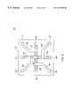
- FIG. 2is an illustration of one embodiment of a functionally symmetric integrated circuit die element having a plurality of interface pads and a corresponding mutually functionally symmetric receptor site having a plurality of corresponding interface pads.
- FIG. 3is a schematic of one embodiment of an integrated circuit in accordance with the teachings of the present invention.
- FIG. 4is an illustration of one embodiment of a layout of an integrated circuit die in accordance of the teachings of the present invention.
- FIG. 5is an illustration of one embodiment of a substrate of an active matrix display having a plurality of pixels and receptor sites in accordance with teachings of the present invention.
- FIG. 6is a schematic of one embodiment of an example circuit in accordance with the teachings of the present invention.
- FIG. 7is a schematic of yet another embodiment of an integrated circuit in accordance with the teachings of the present invention.
- FIG. 8is schematic of still another embodiment of integrated circuit in accordance with the teachings of the present invention.
- FIG. 9is an illustration of another embodiment of a layout of an integrated circuit die in accordance with the teachings of the present invention.
- FIG. 10is an illustration of another embodiment of a substrate of an active matrix display having a plurality of pixels and receptor sites in accordance with the teachings of the present invention.
- FIG. 11is an illustration of another embodiment of a functionally symmetric integrated circuit die element having a plurality of interface pads and a corresponding mutually functionally symmetric receptor site having a plurality of corresponding interface pads.
- FIG. 12is a schematic of another embodiment of integrated circuit in accordance with the teachings of the present invention.
- FIG. 13is a schematic of yet another embodiment of an integrated circuit in accordance with the teachings of the present invention.
- FIG. 14is an illustration of yet another embodiment of a layout of an integrated circuit die in accordance with the teachings of the present invention.
- FIG. 16is an illustration of one embodiment of a wafer including a plurality of integrated circuit dice arranged thereon with testing interconnects disposed across boundary areas in accordance with the teachings of the present invention.
- FIG. 17is an illustration of still another embodiment of a functionally symmetric integrated circuit die element having a plurality of interface pads and a corresponding mutually functionally symmetric receptor site having a plurality of corresponding interface pads.
- FIG. 18is a schematic of still another embodiment of integrated circuit in accordance with the teachings of the present invention.
- FIG. 19is an illustration of still another embodiment of a substrate of an active matrix display having a plurality of pixels, row select lines and analog select lines in accordance with the teachings of the present invention.
- the present inventionrelates to a design and a series of steps and a resulting structure for forming an array of active devices on a substrate which, by way of example, could be plastic, glass or a separately fabricated silicon substrate, among others.
- a substratewhich, by way of example, could be plastic, glass or a separately fabricated silicon substrate, among others.
- One embodiment of the present inventionprovides arrays of elements that can be, for example, individually addressed, driven to a particular voltage or electrically measured. Examples of array structures to which the present invention may be applied include, but are not limited to, displays, x-ray detector panels, solar cell arrays, memory arrays, long wavelength detector arrays, phased arrays of antennas, or the like.
- electronic subelementsincluding small integrated circuit dice that are functionally symmetric under specific rotations are utilized.
- the individual integrated circuit dicehave a trapezoidal cross section.
- the trapezoidal cross section of one embodimenthelp the individual integrated circuit dice to be mounted into receptor sites of another substrate of an electronic device using for example fluidic or vibrational random placement.
- the successfully tested integrated circuit diceare later mounted in an array onto another substrate, which may be formed from many different materials such as for example but not limited to plastic, glass, metal and others, or in layers of one material on another, such as for example plastic on a glass substrate.
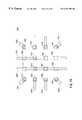
- element 209is an integrated circuit die on a substrate.
- the integrated circuitry of element 209is coupled to a plurality of interface pads 213 , 217 , 219 , 221 , 223 , 225 , 227 , 229 and 231 arranged on one side of element 209 .
- interface pads 233 , 235 , 237 , 239 , 241 , 243 , 245 , 247 and 249 in receptor site 203that are arranged to be coupled to the plurality of interface pads 213 , 217 , 219 , 221 , 223 , 225 , 227 , 229 and 231 when element 209 is mounted in receptor site 203 .
- element 209 and receptor site 203are mutually symmetric such that element 209 can be mounted into receptor site 203 in any one of the plurality of orientations discussed above and the integrated circuit of element 209 will nevertheless provide the proper function for the electronic device of substrate 201 . Therefore, in one embodiment of the present invention, each one of the plurality of interface pads 213 , 217 , 219 , 221 , 223 , 225 , 227 , 229 and 231 are functionally symmetric and therefore provide a predetermined function for the integrated circuit of the element 209 independent of the orientation in which element 209 is mounted in receptor site 203 .
- interface pad 213coupled to either interface pad 233 , 237 , 249 or 245 . It is observed that in the embodiment illustrated in FIG. 2, interface pad 223 of element 209 will be coupled to interface pad 241 of receptor site 203 in all of the possible orientations in which element 209 can be mounted to receptor site 203 .
- integrated circuit 301includes a diode 339 coupled to interface pad 213 and grounded to the substrate 347 of integrated circuit die 301 . It is noted that substrate 347 is also shown as ground in integrated circuit die 301 in FIG. 3.
- a diode 341is coupled to interface pad 219 and grounded to substrate 347 .
- a diode 343is coupled to interface pad 231 and grounded to substrate 347 .
- In a diode 345is coupled to interface pad 227 and grounded to substrate 347 .
- integrated circuit die 301in one embodiment may be included in element 209 , which is mounted in receptor site 203 of substrate 201 of an electronic device.
- at least one of interface pads 213 , 219 , 231 or 227is at ground or zero volts during normal operation of the electronic device of substrate 201 .
- at least one of diodes 339 , 341 , 343 or 345will pull substrate 347 down to zero volts.
- substrate 347rises to a voltage above ground and that interface pad 213 is at ground or zero volts. In this situation, diode 339 will “turn on” to maintain substrate 347 at ground. By maintaining substrate 347 at ground, it is appreciated that the risks of latch up or other undesirable consequences are reduced.
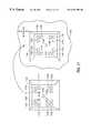
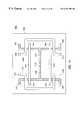
- FIG. 4is an illustration showing one embodiment of a layout of integrated circuit die 401 in a substrate 447 in accordance with the teachings of the present invention.
- the layout of integrated circuit die 401 of FIG. 4corresponds to the schematic illustrated in FIG. 3 .
- semiconductor substrate 447includes silicon.
- substrate 447includes single crystal silicon.
- vias 413 , 417 , 419 , 421 , 423 , 425 , 427 , 429 and 491 of FIG. 4are coupled to interface pads 213 , 217 , 219 , 221 , 223 , 225 , 227 , 229 and 231 , respectively, of FIGS. 2 and 3.
- a channel 431is disposed in substrate 447 between vias 417 and 423 .
- a channel 433is disposed in substrate 447 between vias 425 and 423 .
- a channel 435is disposed in substrate 447 between vias 423 and 429 .
- a channel 437is disposed in substrate 447 between vias 423 and 421 .
- a gate 432is disposed over channel 431 and is coupled to via 419 .
- a gate 434is disposed over channel 433 and is coupled to via 431 .
- a gate 436is disposed over channel 435 and is coupled to via 427 .
- a gate 438is disposed over channel 437 and is coupled to via 413 .
- channel 431 and gate 432 of FIG. 4form transistor 331 of FIG. 3 .
- the channel 433 and gate 434 of FIG. 4form transistor 333 of FIG. 3 .
- the channel 435 and gate 436 of FIG. 4form transistor 335 of FIG. 3 .
- Channel 437 and gate 438 of FIG. 4form transistor 337 of FIG. 3 .
- the layout of integrated circuit 401has four degrees of symmetry, which happens to equal the number of degrees of symmetry of element 209 of FIG. 2 .
- other layouts having different degrees of symmetry than the corresponding elementmay be utilized in other embodiments in accordance with the teachings of the present invention.
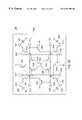
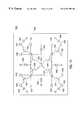
- FIG. 5is an illustration of one embodiment of a portion of a substrate 501 of electronic device.
- the electronic device of substrate 501is an active matrix display.
- substrate 501includes pixels 503 , 505 , 507 and 509 as well as receptor sites 511 , 513 , 515 and 517 .
- receptor sites 511 , 513 , 515 and 517are compatible with the integrated circuit dice discussed above with respect to FIGS. 2-4.
- integrated circuit die 301may be mounted to receptor sites 511 in any one of the above-discussed orientations because both integrated circuit die 501 and receptor site 511 have four degrees of symmetry.
- pixel 503is coupled to interface pad 521 to receptor site 511 .
- Pixel 505is coupled to interface pad 539 of receptor site 513 and interface pad 529 a receptor site 511 .
- Pixel 507is coupled to interface pad 533 of receptor site 511 , interface pad 549 of receptor site 513 and interface pad 567 of receptor site 515 .
- Pixel 509is coupled to interface pad 551 receptor site 513 , interface pad 585 of receptor site 517 and interface pad 575 of receptor site 515 .
- a digital column select line 559is coupled to be received by interface pad 535 of receptor site 511 , interface pad 549 of receptor site 513 , interface pad 581 to receptor site 515 and interface pad 595 of receptor site 517 .
- a digital column select line 561is coupled to be received by interface pad 519 of receptor site 511 , interface pad 541 of receptor site 513 , interface pad 565 of receptor site 515 and interface pad 587 of receptor site 517 .
- digital column select lines 559 and 551are used to activate an entire column of the display of substrate 501 .
- analog row lines 557 and 563are interconnects carrying analog pixel information for the pixels of the display. As shown in FIG. 5, analog row line 557 is coupled to interface pad 527 of receptor site 511 and interface pad 545 of receptor site 513 . Analog row line 563 is coupled to interface pad 573 of receptor site 515 and interface pad 591 of receptor site 517 .
- the analog signal on analog row line 557is coupled to be received by pixel 505 through the interface pads 535 and 539 of receptor site 513 .
- the analog signal on analog row line 557is also coupled to be received by pixel 505 through interface pad 527 and 529 of receptor site 511 .
- the analog signal on row line 563is coupled to be received by pixel 509 through the interface pads 591 and 585 of receptor site 517 .
- the analog signal on row line 563is also coupled to be received by pixel 509 through interface pads 573 and 575 of receptor site 515 . It is noted that because column select 559 is at a logical low value, pixel 503 is not connected to row line 557 through interface pads 527 and 521 of receptor site 511 . Similarly, pixel 507 is not coupled to row line 563 through interface pads 573 and 557 of receptor site 515 . Indeed, pixels 503 and 507 are in a column that has not been selected with column select line 559 .
- each pixel of the display illustrated in FIG. 5is redundantly coupled to receive analog row information through a plurality of receptor sites in accordance with the teachings of the present invention. It is appreciated that this redundancy provides additional reliability to the display of substrate 501 in the event that there is a failure in an integrated circuit device that is included in one of the elements mounted in receptor sites 511 , 513 , 515 or 517 .
- Another characteristic of the display of substrate 501is that whenever a column the selected using, for example, digital column select line 559 or 561 , the entire column of the display is selected. Therefore, in one embodiment, row driver circuitry is required to drive pixel in the entire selected column of the display at a time. For large displays, this may amount to a substantial amount of circuitry to drive every pixel in the column of the display at a time.
- FIG. 6is a schematic of another embodiment of integrated circuit 601 in accordance with the teachings of the present invention.
- integrated circuit 601includes series coupled transistors 603 and 605 between an input 607 and a pixel 609 of a display. As shown in FIG. 6, the gate of transistor 603 is coupled to receive a first digital select signal 611 and the gate of transistor 605 is coupled to receive a second digital select signal 613 .
- an analog input signalis received at input 607 and is coupled to pixel 605 in response to first and second digital select signals 611 and 613 .
- digital select signal 611is a row select signal and digital select signal 613 is a column select signal. In another embodiment, digital select signal 611 is a column select signal and digital select signal 613 is a row select signal.
- each individual pixel 609 of the displaymay be individually addressed. Therefore, it is appreciated that in one embodiment well-known multiplexing techniques may be utilized such that a smaller amount of row driver circuitry is used to drive each pixel 609 of the display in comparison with displays that utilize only a single digital select signal for each pixel.
- the odd columns of pixelsare driven during a first pass of a display refresh cycle and the remaining even columns of pixels are driven during the latter pass of the display refresh cycle. Accordingly, only half the amount of the row driver circuitry is utilized when compared to a display where all columns of pixels are driven during the same pass of a display refresh cycle. It is appreciated of course that there may be other combinations grouping pixels of a display for refresh in accordance with the teachings of the present invention. For instance, the pixels may be divided into odd/even columns of pixels, or the display may be divided into several regions, each of which may be refreshed individually in sequence, etc.
- FIG. 7is a schematic of yet another embodiment of integrated circuit 701 in accordance with the teachings of the present invention.
- transistors 713 and 715are coupled in series between interface pads 730 and 733 .
- Transistors 717 and 719are coupled in series between interface pads 730 and 736 .
- Transistors 721 and 723are coupled in series between interface pads 730 and 739 .
- Transistors 725 and 727are coupled in series between interface pads 730 and 742 .
- integrated circuit 701is used to drive the pixels of a display.
- pixel 703is coupled to interface pad 733
- pixel 705is coupled to interface pad 736
- pixel 707is coupled to interface pad 739
- pixel 709is coupled to interface pad
- interface pad 733is coupled to receive an analog input signal coupled to interface pad 730 through transistors 713 and 715 in response to the first digital select signal coupled to be received at interface pad 731 and a second digital select signal coupled to be received at interface pad 732 .
- Interface pad 736is coupled to receive the analog input signal coupled to interface pad 730 through transistors 717 and 719 in response to a first digital select signal coupled to be received at interface pad 734 and a second digital select signal coupled to be received at interface pad 735 .
- Interface pad 739is coupled to receive the analog input signal coupled to interface pad 730 through transistors 721 and 723 in response to a first digital select signal coupled to be received at interface pad 737 and a second digital select signal coupled to be received at interface pad 738 .
- Interface pad 742is coupled to receive the analog input signal coupled to interface pad 730 through transistors 725 and 727 in response to a first digital select signal coupled to interface pad 740 and a second digital select signal coupled to interface pad 741 .
- integrated circuit 701is yet another integrated circuit that may be implemented into an integrated circuit die having functional symmetry over a plurality of rotational orientations in accordance with the teachings of the present invention.
- integrated circuit 701has four-fold symmetry and 13 separate interface pads 730 - 742 .
- FIG. 8is a schematic of still another integrated circuit 801 in a substrate 849 providing two digital select signals for each pixel in accordance with the teachings of the present invention. It is appreciated that integrated circuit 801 may be included in an element similar to element 209 of FIG. 2 in accordance with the teachings of the present invention.
- interface pads 813 , 817 , 819 , 821 , 823 , 825 , 827 , 839 and 831 of FIG. 8correspond to interface pads 213 , 217 , 219 , 221 , 223 , 225 , 227 , 229 and 231 , respectively, of FIG. 2 .
- Integrated circuit 801includes transistors 833 and 835 coupled in series between interface pads 823 and 813 .
- Transistors 837 and 839are coupled in series between interface pads 823 and 819 .
- Transistors 841 and 843are coupled in series between interface pads 823 and 831 .
- Transistors 845 and 847are coupled in series between interface pads 823 and 827 .
- the gates of transistors 833 and 839are both coupled to interface pad 817 .
- the gates of transistors 837 and 843are both coupled to interface pad 825 .
- the gates of transistors 841 and 847are both coupled to interface pad 829 .
- the gates of transistors 845 and 835are both coupled to interface pad 821 .
- transistors 833 and 839are switched in response to a digital select signal received at interface pad 817 .
- Transistors 837 and 843are switched in response to a digital select signal received at interface pad 825 .
- Transistors 841 and 847are switched in response to a digital select signal received at interface pad 829 transistors 835 and 845 are switched in response to a digital select signal received at interface pad 821 .
- interface pad 813is coupled to interface pad 823 in response to a logical high digital select signal received at interface pads 817 and 821 .
- Interface pad 819is coupled to interface pad 823 in response to the logical high digital select signal received at interface pads 817 and 825 .
- Interface pad 831is coupled to interface pad 823 in response to a logical high digital select signal received at interface pads 825 and 829 .
- Interface pad 827is coupled to interface pad 823 in response to a logical high digital select signal received at interface pads 821 and 829 .
- integrated circuit 801is utilized in one embodiment to drive pixels of an active matrix display from an analog signal line coupled to interface pad 823 , it is worthwhile to note that integrated circuit 801 provides the individual addressability of pixels coupled to interface pads 813 , 819 , 827 and 831 using nine interface pads 813 , 817 , 819 , 821 , 823 , 825 , 827 , 829 and 831 instead of the 13 interface pads 730 - 742 employed in FIG. 7 .
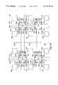
- FIG. 9is an illustration showing one embodiment of a layout of an integrated circuit die 901 in a substrate 947 in accordance with the teachings of the present invention.
- the layout of integrated circuit die 901corresponds to the schematic illustrated in FIG. 8 .
- semiconductor substrate 947includes silicon.
- substrate 947includes single crystal silicon.
- vias 913 , 917 , 919 , 921 , 923 , 925 , 927 , 929 and 931are coupled to interface pads 813 , 817 , 819 , 821 , 823 , 825 , 827 , 829 and 831 , respectively, of FIG. 8 .
- a channel 931is disposed in substrate 947 between vias 913 and 923 .
- a channel 933is disposed in substrate 947 between vias 919 and 923 .
- a channel 935is disposed in substrate 947 between vias 931 and 923 .
- a channel 937is disposed in substrate 947 between vias 927 and 923 .
- gates 932 and 946are disposed over channel 931 .
- Gates 932 and 946are coupled to vias 917 and 921 , respectively.
- Gates 936 and 934are disposed over channel 933 .
- Gates 936 and 934are coupled to vias 925 and 917 , respectively.
- Gates 940 and 938are disposed over channel 935 .
- Gates 940 and 938are coupled to vias 929 and 925 , respectively.
- Gates 944 and 942are disposed over channel 937 .
- Gates 944 and 942are coupled to vias 921 and 929 , respectively.
- channel 931 and gates 932 and 946form transistors 838 and 835 , respectively.
- Channel 933 and gates 934 and 936 aform transistors 839 and 833 , respectively.
- Channel 935 and gates 938 and 940form transistors 843 and 841 , respectively.
- Channel 937 and gates 942 and 944form transistors 847 and 845 , respectively.
- the layout of integrated circuit 901has four degrees of symmetry, which happens to equal the number of degrees of symmetry of element 209 of FIG. 2 .
- other layouts having different degrees of symmetry than corresponding elementmay be utilized in other embodiments in accordance with the teachings of the present invention.
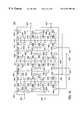
- FIG. 10is an illustration of another embodiment of a portion of a substrate 1001 of the electronic device.
- the electronic device of substrate 1001is an active matrix display.
- substrate 1001includes pixels 1003 , 1005 , 1007 and 1009 as well as receptor sites 1025 , 1027 , 1029 and 1031 .
- receptor sites 1025 , 1027 , 1029 and 1031are compatible with the integrated circuit dice discussed above with respect to FIGS. 8 and 9.
- integrated circuit die 801may be mounted on to receptor site 1025 in any one of four orientations as discussed above because integrated circuit 801 has four-fold symmetry.
- pixel 1003is coupled to interface pad 1037 of receptor site 1025 .
- Pixel 1005is coupled to interface pad 1053 of receptor site 1027 and interface pad 1033 of receptor site 1025 .
- Pixel 1007is coupled to interface pad 1071 of receptor site 1029 .
- Pixel 1009is coupled to interface pad 1089 of receptor site 1031 and interface pad 1067 of receptor site 1029 .
- digital column select line 1011is coupled to be received at interface pad 1041 of receptor site 1025 , interface pad 1055 of receptor site 1027 , interface pad 1077 of receptor site 1029 and interface pad 1091 of receptor site 1031 .
- digital column select line 1011is used to select the column including pixels 1005 and 1009 .
- the active matrix display of substrate 1001also includes a digital row select lines 1015 , 1017 , 1021 and 1023 .
- Digital row select line 1015is coupled to be received by interface pad 1035 of receptor site 1025 and interface pad 1051 of receptor site 1027 .
- Digital row select line 1017is coupled to received by interface pad 1045 of receptor site 1025 and interface pad 1063 of receptor site 1027 .
- Digital row select line 1021is coupled to be received by interface pad 1069 of receptor site 1029 and interface pad 1087 of receptor site 1031 .
- Digital row select line 1023is coupled to be received by interface pad 1081 of receptor site 1029 and interface pad 1098 of receptor site 1031 .
- digital row select line 1015is used to select the row of the display including pixels 1003 and 1005 .
- Digital row select lines 1017 and 1021are used to select the row of the display including pixels 1007 and 1009 .
- analog lines 1013 and 1019carry analog pixel information for the pixels of the display. As shown in FIG. 10, analog line 1013 is coupled to be received by interface pad 1040 of receptor site 1025 and interface pad 1057 of receptor site 1027 . Analog line 1019 is coupled to be received by interface pad 1075 of receptor site 1029 and interface pad 1093 of receptor site 1031 .
- each pixel in the display illustrated in FIG. 10is redundantly coupled to receive analog information from a plurality of receptor sites in accordance with the teachings of the present invention. It is appreciated that this redundancy provides additional reliability to the display of substrate 1001 in the event that there is a failure in an integrated circuit device that is included in one of the elements mounted in receptor sites 1025 , 1027 , 1029 and 1031 .
- One characteristic of the display of substrate 1001is that several layers of metalization are utilized to interconnect the elements of the display. Accordingly, a plurality of masking steps are required during fabrication of the display of the substrate 1001 . As consequence, there are crossovers between overlapping interconnect lines in neighboring layers of metalization. For example, as shown in FIG. 10 digital column select line 1011 crosses over a plurality of other interconnect lines including analog line 1013 , digital row select line 1015 , etc. As can be appreciated, the crossover of interconnect lines is a potential source for interlayer short circuit defects between interconnect lines.
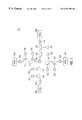
- FIG. 11is an illustration of yet another embodiment of an element 1105 and a corresponding receptor site 1103 in a substrate 1101 in accordance with the teachings of the present invention.
- the cross-section of element 1105 in one embodimentis trapezoidal.
- the trapezoidal cross-section of the elements of one embodiment of the present inventionhelp element 1105 to be mounted into receptor site 1103 using fluidic self-assembly, vibrational tables, or the like.
- element 1105 and receptor site 1103are mutually symmetric such that element 1105 may be mounted into receptor site 1103 in any one of a plurality of orientations relative to receptor site 1103 .
- element 1105is an integrated circuit die on a substrate.
- the integrated circuitry of element 1105is coupled to a plurality of interface pads 1107 , 1109 , 1111 , 1113 , 1115 , 1117 , 1119 , 1121 , 1123 , 1125 , 1127 , 1129 and 1131 , which are arranged on the substrate of element 1105 .
- interface pads 1133 , 1135 , 1137 , 1139 , 1141 , 1143 , 1145 , 1137 , 1149 , 1151 , 1153 , 1155 and 1157arranged in receptor site 1103 .
- the above referenced interface padsare arranged in a pattern such that the interface pads of element 1105 and the interface pads of receptor site 1103 are coupled when element 1105 is mounted in receptor site 1103 in any one of a plurality of rotations.
- the integrated circuit of element 1105will provide proper function for an electronic device of substrate 1101 .
- the top of FIG. 11is “North” and that arrow 1106 is fixed on element 1105 as shown in FIG. 11 .
- element 1105 and receptor site 1103each have four-fold or four degrees symmetry.
- element 1105may be mounted into receptor site 1103 with arrow 1106 pointing either “North,” “East,” “South” or “West.”
- FIG. 12is a schematic of one embodiment integrated circuit 1201 that may be included in element 1105 in accordance with the teachings of the present invention.
- integrated circuit 1201include transistors 1235 and 1233 coupled between interface pads 1219 and 1207 .
- Transistors 1239 and 1237are coupled between interface pads 1213 and 1219 .
- Transistors 1243 and 1241are coupled between interface pads 1231 and 1219 .
- Transistors 1245 and 1237are coupled between interface pads 1219 and 1225 .
- the gates of transistors 1233 and 1245are coupled to interface pads 1209 and 1227 .
- the gates of transistors 1237 and 1241are coupled to interface pads 1211 and 1229 .
- the gates of transistors 1239 and 1235are coupled to interface pads 1217 and 1215 .
- the gates of transistors 1243 and 1237are coupled to interface pads 1223 and 1221 .
- integrated circuit 1201provides direct crossover paths between several pairs of the interface pads. These crossover paths act as pass-through conduits.
- interface pad 1217is directly coupled to interface pad 1215
- interface pad 1223is directly coupled to interface pad 1221
- interface pad 1211it directly coupled to interface pad 1229
- interface pad 1209is directly coupled to interface pad 1227 .
- this direct coupling of pairs of interface padsprovides crossover paths within integrated circuit 1201 , which in one embodiment eliminates the need for multiple metalization layers of a completed electronic device utilizing integrated circuit 1201 .
- interface pad 1219is coupled to interface pad 1207 when a logical high signal is received at interface pads 1209 / 1227 and interface pads 1215 / 1217 .
- Interface pad 1213is coupled to interface pad 1219 when a logical high signal is received at interface pads 1211 / 1229 and 1215 / 1217 .
- Interface pad 1231is coupled to interface pad 1219 when the logical high signal is received at interface pads 1211 / 1229 and interface pads 1221 / 1223 .
- Interface pad 1225is coupled to interface pad 1219 when a logical high signal is received at interface pads 1209 / 1227 and interface pads 1221 / 1223 .
- integrated circuit 1201includes sample and hold circuitry coupled to interface pads 1207 , 1213 , 1225 and 1291 .
- the sample and hold circuitryincludes a capacitor 1257 grounding interface pad 1207 to the substrate 1265 integrated circuit 1201 .
- a capacitor 1259grounds interface pad 1213 to substrate 1265
- a capacitor 1263grounds interface pad 1225 to substrate 1265
- a capacitor 1261grounds interface pad 1231 to substrate 1265 .
- connections to groundmay also be considered as connections to substrate 1265 of integrated circuit die 1201 .
- interface pads 1211 / 1229 and 1209 / 1227are coupled to receive either digital row select or digital column select signals of an active matrix display.
- interface pads 1215 / 1217 and interface pads 1221 / 1253are coupled to receive either digital column select or digital row select signals of the active matrix display.
- interface pads 1211 / 1229receive a logical high signal
- interface pads 1209 / 1227receive a logical low signal
- interface pads 1209 / 1227receive a logical high signal
- interface pads 1211 / 1229receive a logical low signal
- interface pads 1215 / 1217receive a logical high signal
- interface pads 1221 / 1223receive a logical low signal
- interface pads 1221 / 1223receive a logical low signal.
- interface pads 1221 / 1223receive a logical high signal
- interface pads 1215 / 1217receive a logical low signal.
- integrated circuit die 1201 in one embodimentis included in element 1105 , which is mounted in receptor site 113 of substrate 1101 .
- a transistor 1249is coupled between interface pads 1209 / 1227 and the substrate 1265 , which is illustrated as ground in FIG. 12 .
- transistor 1251is coupled between interface pads 1215 / 1217 and substrate 1265
- transistor 1253is coupled between interface pads 1211 / 1229 and substrate 1265
- transistor 1255is coupled between interface pads 1221 / 1223 and substrate 1265 .
- transistor 1249couples substrate 1265 to interface pads 1209 / 1227 in response to the logical high value received at interface pads 1211 / 1229 .
- the logical high valuereceived at interface pads 1211 / 1229 .
- transistor 1253couples substrate 1265 to interface pads 1211 / 1229 in response to a logical high signal received at interface pads 1209 / 1227 .
- interface pads 1209 / 1227are at the logical high value, it is assumed that interface pads 1211 / 1229 are at the logical low value.
- substrate 1265will be maintained at the ground or the logical low value during this time.
- transistor 1251couples substrate 1265 to interface pads 1215 / 1217 in response to a logical high value received at interface pads 1221 / 1223 .
- a logical high valuereceived at interface pads 1221 / 1223 .
- transistor 1255couples substrate 1265 to interface pads 1221 / 1223 in response to a logical high signal received at interface pads 1215 / 1217 .
- interface pads 1215 / 1217are at the logical high value
- interface pads 1221 / 1223are at the logical low value.
- substrate 1265will be maintained at the ground or the logical low value during this time.
- the risks of latch up or other undesirable consequencesare reduced.
- FIG. 13is a schematic of another embodiment of an integrated circuit die 1301 in accordance with the teachings of the present invention.
- Integrated circuit die 1301is similar to integrated circuit die 1201 and interface pads 1307 , 1309 , 1311 , 1313 , 1315 , 1317 , 1319 , 1321 , 1323 , 1325 , 1327 , 1329 and 1331 correspond to interface pads 1207 , 1209 , 1211 , 1213 , 1215 , 1217 , 1219 , 1221 , 1223 , 1225 , 1257 , 1229 and 1231 , respectively.
- Transistors 1333 , 1335 , 1337 , 1339 , 1341 , 1343 , 1345 and 1347correspond to transistors 1233 , 1235 , 1237 , 1239 , 1241 , 1243 , 1245 and 1237 , respectively.
- Sample and hold circuitry capacitors 1357 , 1359 , 1361 and 1363correspond to capacitors 1257 , 1259 , 1261 and 1263 , respectively.
- interface pads 1311 / 1329are at a high logical value
- interface pads 1309 / 1327are at a low logical value and vice versa.
- interface pads 1315 / 1317are at a high logical value
- interface pads 1321 and 1323are at the low logical value or vice versa.
- At least one of the diodes 1349 , 1351 , 1353 or 1355will pull substrate 1365 down to zero volts. For example, assume that substrate 1365 rises to a voltage greater than zero volts and that interface pads 1317 / 1315 are at zero volts. In this situation, diode 1349 will “turn on” to maintain substrate 1365 at ground. Operation of diodes 1351 , 1353 and 1355 is similar. By maintaining substrate 1365 at zero volts, it is appreciated that the risks of latch up other undesirable consequences are reduced.
- FIG. 14is an illustration showing one embodiment of a layout of an integrated circuit die 1401 in a substrate 1445 in accordance with the teachings of the present invention.
- the layout of integrated circuit die 1401 of FIG. 14corresponds to either one of the embodiments illustrated in FIGS. 12 or 13 .
- substrate 1445is a semiconductor substrate including silicon.
- substrate 1445is a semiconductor substrate including single crystal silicon.
- integrated circuit dieincludes vias 1407 , 1409 , 1411 , 1413 , 1415 , 1417 , 1419 , 1421 , 1423 , 1425 , 1427 , 1459 and 1431 .
- the vias of the integrated circuit die 1401are coupled to interface pads 1207 , 1209 , 1211 , 1213 , 1215 , 1217 , 1219 , 1221 , 1223 , 1225 , 1227 , 1229 or 1231 , respectively.
- a channel 1433is disposed in substrate 1445 and is coupled between interface pads 1419 and 1407 .
- Channel 1433is also coupled between interface pads 1419 and 1425 .
- a channel 1435is disposed and substrate 1445 and is coupled between interface pads 1413 and 1419 .
- Channel 1435is also coupled between interface pad 1431 and 1419 .
- a gate 1441is coupled between interface pads 1415 and 1417 and is disposed over a portion of channel 1435 between interface pads 1413 and 1419 .
- Gate 1441is also disposed over a portion of channel 1433 disposed between interface pads 1407 and 1419 .
- a gate 1443is coupled between interface pads 1421 and 1423 .
- Gate 1443is disposed over a portion of channel 1435 between interface pads 1419 and 1431 .
- Gate 1443is also disposed over a portion of channel 1433 between interface pads 1419 and 1425 .
- a gate 1437is coupled between interface pads 1411 and 1429 and is disposed over a portion of channel 1435 between interface pads 1413 and 1419 .
- Gate 1437is also disposed over a portion of channel 1435 between interface pads 1419 and 1431 .
- a gate 1439is disposed between interface pads 1409 and 1427 and is disposed over a portion of channel 1433 between interface pads 1419 and 1407 .
- Gate 1439is also disposed over a portion of channel 1433 between interface pads 1419 and 1425 .
- gate 1437provides a direct crossover path or pass-through conduit between interface pads 1411 and 1429 .
- Gate 1439provides a direct crossover path between interface pads 1409 and 1427 .
- Gate 1441provides a direct crossover path between interface pads 1415 and 1417 .
- Gate 1443provides a direct crossover path between interface pads 1421 and 1423 .
- the layout of integrated circuit die 1401has two degrees of symmetry, even though element 1105 has four degrees of symmetry. Therefore, it is appreciated that the layout of an integrated circuit die in accordance with teachings of the present invention may have a different number of degrees of symmetry than the corresponding element.
- a plurality of integrated circuit dice having the schematics of integrated circuit die 1201may be mounted into receptor sites 1529 , 1531 , 1533 and 1535 in any one of the above discussed plurality of orientations to enable the active matrix display of substrate 1501 to function properly.
- only one layer of metalizationand therefore only one masking step, is needed after the integrated circuit dice are mounted into receptor sites 1529 , 1531 , 1533 and 1535 .
- only one masking stepis needed in one embodiment of the present invention.
- interface pads 1547 , 1545 , 1573 and 1571are coupled to receive one digital row select signal.
- Interface pads 1553 , 1551 , 1579 , 1577 , 1599 , 1597 , 1528 and 1524are coupled to receive another digital row select signal.
- Interface pads 1506 , 1504 , 1534 and 1532are coupled to receive yet another digital row select signal.
- digital column select line 1554is used to select the column of the active matrix display of substrate 1501 including pixels 1505 , 1513 and 1521 .
- Digital column select line 1556is used to select the column including pixels 1507 , 1515 and 1523 .
- Digital column select line 1558is used to select the column including pixels 1509 , 1517 and 1525 .
- Digital column select line 1560is used to select the column including pixels 1511 , 1519 and 1527 .
- the digital row select line coupled to be received by interface pads 1547 , 1545 , 1573 and 1571is used to select the row of pixels including pixels 1505 , 1507 , 1509 and 1511 .
- the digital row select line coupled to be received by interface pads 1553 , 1551 , 1579 , 1577 , 1599 , 1597 , 1528 and 1524is used to select the row Of pixels including pixels 1513 , 1515 , 1517 and 1519 .
- the digital row select line coupled to be received by interface pads 1506 , 1904 , 1994 and 1532is used to select the row of pixels including pixels 1521 , 1523 , 1525 and 1527 .
- analog line 1550carries analog pixel information and is coupled to be received by interface pad 1549 of receptor site 1529 and interface pad 1502 of receptor site 1533 .
- Analog line 1552also carries pixel information and is coupled to be received by interface pad 1575 of receptor site 1531 and interface pad 1513 of receptor site 1535 .
- digital column select lines 1556 and 1560are set to a logical high value and that digital column select lines 1554 and 1558 are set to a logical low value.
- the columns of pixels including pixels 1507 , 1515 and 1553 as well as pixels 1511 , 1519 and 1527are selected.
- the columns including pixels 1505 , 1513 and 1521 as well as pixels 1509 , 1517 and 1525are deselected.
- the digital row select signal coupled to be received by interface pads 1553 , 1551 , 1579 , 1577 , 1599 , 1597 , 1528 and 1524is set to a logical high value.
- the digital row select signals coupled to be received by interface pads 1547 , 1545 , 1573 , 1571 , 1506 , 1504 , 1534 and 1532are set to a logical low value.
- the row of pixels in the active matrix display of substrate 1501 including pixels 1513 , 1515 , 1517 and 1519is selected.
- the rows of pixels including pixels 1505 , 1507 , 1509 , 1511 , 1521 , 1523 , 1525 and 1527are deselected.
- pixels 1515 and 1519are individually selected while the remaining pixels are deselected.
- the analog information carried in analog line 1515is coupled to be received by pixel 1515 from interface pad 1549 through interface pad 1555 .
- the analog information carried in analog line 1515is also coupled to be received by pixel 1515 from interface pad 1502 through interface pad 1589 .
- the analog information carried in analog line 1552is coupled to be received by pixel 1519 from interface pad 1575 through interface pads 1581 .
- the analog information carried in analog line 1552is also coupled to be received by pixel 1519 from interface pad 1530 through interface pad 1516 . It is appreciated that the remaining pixels shown in FIG. 15, with the digital row and column select lines set as described above, are deselected and are therefore not coupled to receive analog information from analog lines 1550 and 1552 .
- each pixel 1505 , 1507 , 1509 , 1511 , 1513 , 1515 , 1517 , 1519 , 1521 , 1523 , 1525 and 1527 of the active matrix display illustrated in FIG. 15is redundantly coupled to receive analog pixel information through a plurality of receptor sites in accordance with the teachings of the present invention. Is appreciated that this redundancy provides additional reliability to the active matrix display of FIG. 15 in the event that there is a failure in an integrated circuit device that is mounted in receptor sites 1529 , 1531 , 1533 or 1535 .
- FIG. 16is an illustration of a wafer 1601 in accordance with the teachings of the present invention.
- a plurality of integrated circuit dice 1603 , 1605 , 1607 and 1609are fabricated arranged on an individual wafer 1601 .
- a boundary area 1611 of wafer 1601is removed to separate integrated circuit dice 1603 , 1605 , 1607 and 1609 from each other.
- wafer 1601includes testing interconnects coupled between some of the interface pads of the integrated circuit dice of wafer 1601 . These testing interconnects enable testing of each of the integrated circuit dice included in wafer 1601 .
- integrated circuit dice 1603 , 1605 , 1607 and 1609correspond to the integrated circuit dice discussed above with respect to FIGS. 11-14, and may be utilized in the receptor sites of FIG. 15 .
- the function of interface pads 1637 , 1639 , 1641 , 1643 , 1653 , 1655 , 1661 , 1665 , 1667 , 1673 , 1675 , 1677 and 1679correspond to the function of interface pads 1413 , 1411 , 1409 , 1407 , 1417 , 1415 , 1419 , 1423 , 1421 , 1431 , 1429 , 1427 and 1425 , respectively.
- interface pads 1645 , 1647 , 1649 , 1651 , 1657 , 1659 , 1663 , 1669 , 1671 , 1681 , 1683 , 1685 and 1687correspond to the function of interface pads 1413 , 1411 , 1409 , 1407 , 1417 , 1415 , 1419 , 1423 , 1421 , 1431 , 1429 , 1427 and 1425 , respectively.
- interface pads 1697 , 1699 , 1602 , 1604 , 1610 , 1612 , 1616 , 1622 , 1624 , 1634 , 1636 , 1638 and 1640correspond to the function of interface pads 1413 , 1411 , 1409 , 1407 , 1417 , 1415 , 1419 , 1423 , 1421 , 1431 , 1429 , 1427 and 1425 , respectively.
- interface pads 1656 , 1658 , 1660 , 1662 , 1664 , 1666 and 1668also correspond to the function of interface pads 1409 , 1407 , 1445 , 1419 , 1421 , 1427 and 1425 .
- the function of interface pads 1670 , 1672 , 1674 , 1676 , 1678 , 1680 and 1682correspond to the function of interface pads 1413 , 1411 , 1417 , 1419 , 1423 , 1431 and 1429 .
- interface pads 1684 , 1686 , 1688 , 1690 , 1692 , 1694 and 1696also correspond to the function of interface pads 1413 , 1411 , 1417 , 1419 , 1423 , 1431 and 1429 .
- wafer 1601includes testing interconnects coupling across boundary area 1611 interface pads 1644 and 1637 , 1646 and 1653 , 1650 and 1665 , 1654 and 1673 , 1658 and 1689 , 1660 and 1606 , 1664 and 1618 , 1668 and 1626 , 1643 and 1645 , 1655 and 1657 , 1667 and 1669 , 1679 and 1681 , 1695 and 1697 , 1608 and 1610 , 1620 and 1622 , 1632 and 1634 , 1651 and 1670 , 1659 and 1674 , 1671 and 1678 , 1687 and 1680 , 1604 and 1684 , 1612 and 1688 , 1624 and 1692 and 1640 and 1694 .
- Wafer 1601also includes testing interconnects coupled between interface pads 1648 and 1662 , 1652 and 1656 , 1682 and 1686 and 1676 and 1690 . Furthermore, wafer 1601 includes interconnects 1613 , 1615 , 1617 and 1619 to access interface pads 1648 , 1651 , 1663 and 1676 , respectively.
- one embodiment of wafer 1601also includes digital row select line 1621 coupled to be received by interface pad 1646 .
- Digital row select line 1623is coupled to be received by interface pad 1678 .
- Digital row select line 1625is coupled to be received by interface pads 1660 .
- Digital row select line 1627is coupled to be received by interface pad 1692 .
- wafer 1601also includes digital column select line 1629 coupled to interface pads 1628 and 1696 .
- Digital column select line 1631is coupled to interface pad 1630 .
- Digital column select line 1633coupled to interface pads 1666 and 1636 .
- Digital column select line 1635coupled to interface pad 1638 .
- Testing of the integrated circuit dice 1603 , 1605 , 1607 and 1609 of wafer 1601may be conducted as follows.
- digital row select line 1621 and digital column select lines 1629 and 1633are set to logical high value while digital row select lines 1623 , 1625 and 1627 and digital column select line 1631 are set to a logical low value. It is appreciated that by setting the digital column in row select lines as described above, the switchable coupling between interface pads 1648 and 1661 is also switched on. By setting the digital column and row select lines to settings other than those described above, the switchable couplings between interface pads 1648 and 1661 and interface pads 1661 and 1637 is switched off.
- the switchable couplingsmay be tested through testing interconnects 1613 and 1615 .
- interface pads 1646 and 1653receive a logical high value.
- interface pads 1642 and 1639receive logical high values. It is reminded that interface pad 1642 receives the logical high value from digital column select line 1633 through the direct crossover connection between interface pads 1642 and 1652 , the testing interconnect between interface pads 1652 and 1656 and the direct crossover connection between interface pads 1656 and 1666 .
- interface pad 1639receives the logical high value from digital column select line 1629 through the direct crossover connection between interface pads 1639 and 1675 , the testing interconnect between interface pads 1675 and 1691 and the direct crossover connection between interface pads 1691 and 1628 . Therefore, the coupling between testing interconnects 1613 and 1615 through interface pad 1648 from interface pad 1644 , through the testing interconnect between interface pads 1644 and 1637 and from interface pad 1637 through interface pad 1661 .
- the integrated circuit devices in connection with the switchable coupling between interface pads 1663 and 1651may be tested concurrently with the testing of the integrated circuit devices in connection with the switchable coupling between interface pads 1661 and 1637 .
- a switchable couplingcan be verified between interface pads 1648 and 1661 and 1663 and 1676 concurrently in accordance with the teachings of the present invention.
- interface pads 1659 and 1674as well as interface pads 1646 and 1653 receive the logical high value.
- interface pads 1639 and 1675 , 1672 and 1682as well as 1649 and 1685 receive logical high values.
- the switchable coupling that can be verified between testing interconnects 1617 and 1619is a from interface pad 1663 through interface pad 1651 , through the testing interconnect between interface pads 1651 and 1670 , and from interface pads 1670 through interface pad 1676 .
- testingmay continue to the next switchable couplings in the integrated circuit dice of wafer 1601 by setting the digital column and row select lines of wafer 1601 accordingly.
- the switchable coupling between interface pads 1637 and 1661may be tested by setting digital row select line 1621 to logical low value and setting digital row select line 1623 to a high logical value.
- the digital column select lines settingsremain unchanged.
- the switchable coupling between interface pads 1689 and 1614may be tested by setting digital row select line to a logical low value and setting digital row select line 1625 to logical high value.
- the digital column select line valuesremain unchanged.
- digital row select line 1625is set to the logical low value and digital row select line 1627 is set to high logical value.
- digital column select line valuesremain in change. Next, testing can proceed to the another column in accordance with the teachings of the present invention.
- the integrated circuit dicemay be separated and utilized in accordance with the teachings of the present invention.
- the defective integrated circuit diemay be marked and set aside while the remaining properly functioning integrated circuit dice may be utilized.
- integrated circuit dice 1603 , 1605 , 1607 and 1609are separated by removing the boundary area 1611 of wafer 1601 .
- boundary area 1611By removing boundary area 1611 , is noted that the testing interconnects crossing boundary area 1611 are severed. In one embodiment, it is noted that the severing of these testing interconnects between the interface pads of neighboring integrated circuit dice is acceptable after testing of the corresponding wafer has been completed as the testing interconnects are no longer are utilized.
- FIG. 16is merely in one embodiment of a wafer including a plurality of integrated circuit dice arranged therein. It is appreciated that other embodiments of wafer is, such as for example a wafer including a larger or smaller number of integrated circuit dice arranged thereon, may also be tested in accordance with teachings of the present invention.
- FIG. 17is an illustration of yet another embodiment of an element 1705 and a corresponding receptor site 1703 in a substrate 1701 in accordance with the teachings of the present invention.
- the cross-section of element 1705 in one embodimentis trapezoidal.
- the trapezoidal cross-section of the elements of one embodiment of the present inventionhelp element 1705 to be mounted into receptor site 1703 using fluidic self-assembly, vibrational tables, or the like.
- element 1705 and receptor site 1703are mutually symmetric such that element 1705 may be mounted into receptor site 1703 in any one of a plurality of orientations relative to receptor site 1703 .
- element 1705is an integrated circuit die on a substrate.
- the integrated circuitry of element 1705is coupled to a plurality of interface pads 1707 , 1709 , 1717 , 1713 , 1715 , 1717 , 1719 , 1721 , 1723 , 1725 , 1727 , 1729 , 1731 , 1733 , 1735 and 1737 which are arranged on the substrate of element 1705 .
- the above referenced interface padsare arranged in a pattern such that the interface pads of element 1705 and the interface pads of receptor site 1703 are coupled when element 1705 is mounted in receptor site 1703 in any one of a plurality of rotations.
- the integrated circuit of element 1705When mounted in any one of the plurality of orientations, the integrated circuit of element 1705 will provide proper function for an electronic device of substrate 1701 .
- the top of FIG. 17is “North” and that arrow 1706 is fixed on element 1705 as shown in FIG. 17 .
- element 1705 and receptor site 1703each have four-fold or four degrees symmetry.
- element 1705may be mounted into receptor site 1703 with arrow 1706 pointing either “North,” “East,” “South” or “West.”
- FIG. 18is a schematic of one embodiment integrated circuit 1801 that may be included in element 1705 in accordance with the teachings of the present invention.
- integrated circuit 1801includes transistors 1839 and 1841 coupled between interface pads 1807 and 1817 .
- Transistors 1843 and 1845are coupled between interface pads 1813 and 1819 .
- Transistors 1847 and 1849are coupled between interface pads 1825 and 1831 .
- Transistors 1851 and 1853are coupled between interface pads 1827 and 1837 .
- the gate of transistor 1839is coupled to interface pad 1809 and the gate of transistor 1841 is coupled to interface pad 1815 .
- the gate of transistor 1843is coupled to interface pad 1811 and the gate of transistor 1845 is coupled to interface pad 1821 .
- the gate of transistor 1847is coupled to interface pad 1823 and the gate of transistor 1849 is coupled to interface pad 1853 .
- the gate of transistor 1851is coupled to interface pad 1829 and the gate of transistor 1853 is coupled to interface pad 1835 .
- integrated circuit 1801provides direct crossover paths or pass-through conduits between several pairs of the interface pads.
- interface pad 1809is directly coupled to interface pad 1833 through crossover path 1861 .
- Interface pad 1811is directly coupled to interface pad 1835 through crossover path 1859 .
- Interface pad 1821is directly coupled to interface pad 1815 through crossover path 1855 .
- Interface pad 1829is directly coupled to interface pad 1823 through crossover path 1857 .
- crossover paths 1855 , 1857 , 1859 and 1861eliminate the need for multiple metalization layers of a completed electronic device utilizing integrated circuit 1801 .
- interface pad 1817is coupled to interface pad 1807 when a logical high signal is received on interface pads 1809 / 1833 or 1815 / 1821 .
- Interface pad 1819is coupled to interface pad 1813 when a logical high signal is received on interface pads 1811 / 1835 or 1821 / 1815 .
- Interface pad 1827is coupled to interface pad 1837 when a logical high signal is received on interface pads 1829 / 1823 or 1835 / 1811 .
- Interface pad 1825is coupled to interface pad 1831 when a logical high signal is received on interface pads 1823 / 1829 or 1833 / 1809 .
- FIG. 19is an illustration of one embodiment of a receptor site 1901 of the substrate of an electronic device.
- the electronic deviceis an active matrix display.
- receptor site 1501includes interface pads 1907 , 1913 , 1915 , 1917 , 1919 , 1921 , 1923 , 1925 , 1927 , 1929 , 1931 and 1937 .
- a pixelis coupled to interface pad 1907 through connection 1953 and to interface pad 1931 through connection 1957 .
- Another pixelis coupled to interface pad 1913 through connection 1951 and to interface pad 1937 through connection 1955 .
- receptor sites 1901is compatible with the integrated circuit die discussed above with respect to FIGS. 17 and 18.
- a plurality of integrated circuit dice having the schematics of integrated circuit die 1801may be mounted into receptor site 1901 in any one of the above discussed plurality of orientations to enable the active matrix display of receptor site 1501 to function properly.
- a digital row select line 1943is coupled to be received by interface pads 1921 .
- interface pad 1915is coupled to interface pad 1921 through a crossover connection.
- a digital row select line 1945is coupled to be received by interface pad 1929 .
- interface pad 1923is coupled to interface pad 1929 through a crossover connection.
- an analog line 1939is coupled to interface pads 1919 and 1927 . Note that in this embodiment, analog line 1939 is not coupled to region 1911 and region 1935 .
- An analog line 1941is coupled to interface pads 1917 and 1925 . Note that in this embodiment, analog line 1941 is not coupled to region 1909 and region 1933 .
- analog line 1939carries analog pixel information to drive pixels coupled to interface pads 1913 and 1937 , which are selected by signals carried on digital row select lines 1943 and 1945 .
- Analog line 1941carries analog pixel information to drive pixels coupled to interface pads 1907 and 1931 , which are selected by signals carried on digital row select lines 1943 and 1945 .
Landscapes
- Engineering & Computer Science (AREA)
- Power Engineering (AREA)
- Physics & Mathematics (AREA)
- Computer Hardware Design (AREA)
- Microelectronics & Electronic Packaging (AREA)
- General Physics & Mathematics (AREA)
- Condensed Matter Physics & Semiconductors (AREA)
- Crystallography & Structural Chemistry (AREA)
- Theoretical Computer Science (AREA)
- Chemical & Material Sciences (AREA)
- Geometry (AREA)
- Semiconductor Integrated Circuits (AREA)
- Liquid Crystal (AREA)
- Design And Manufacture Of Integrated Circuits (AREA)
Abstract
Description
Claims (80)
Priority Applications (5)
| Application Number | Priority Date | Filing Date | Title |
|---|---|---|---|
| US09/251,220US6291896B1 (en) | 1999-02-16 | 1999-02-16 | Functionally symmetric integrated circuit die |
| JP2000600307AJP2002537656A (en) | 1999-02-16 | 2000-01-24 | Functionally symmetric integrated circuit die |
| EP00909964AEP1155450A1 (en) | 1999-02-16 | 2000-01-24 | Functionally symmetric integrated circuit die |
| PCT/US2000/001706WO2000049658A1 (en) | 1999-02-16 | 2000-01-24 | Functionally symmetric integrated circuit die |
| AU32136/00AAU3213600A (en) | 1999-02-16 | 2000-01-24 | Functionally symmetric integrated circuit die |
Applications Claiming Priority (1)
| Application Number | Priority Date | Filing Date | Title |
|---|---|---|---|
| US09/251,220US6291896B1 (en) | 1999-02-16 | 1999-02-16 | Functionally symmetric integrated circuit die |
Publications (1)
| Publication Number | Publication Date |
|---|---|
| US6291896B1true US6291896B1 (en) | 2001-09-18 |
Family
ID=22950994
Family Applications (1)
| Application Number | Title | Priority Date | Filing Date |
|---|---|---|---|
| US09/251,220Expired - LifetimeUS6291896B1 (en) | 1999-02-16 | 1999-02-16 | Functionally symmetric integrated circuit die |
Country Status (5)
| Country | Link |
|---|---|
| US (1) | US6291896B1 (en) |
| EP (1) | EP1155450A1 (en) |
| JP (1) | JP2002537656A (en) |
| AU (1) | AU3213600A (en) |
| WO (1) | WO2000049658A1 (en) |
Cited By (109)
| Publication number | Priority date | Publication date | Assignee | Title |
|---|---|---|---|---|
| US20020158577A1 (en)* | 2000-07-07 | 2002-10-31 | Tatsuya Shimoda | Organic electroluminescent display and manufacturing method thereof, electro-optic device and manufacturing method thereof, and electronic device |
| US6590346B1 (en)* | 2001-07-16 | 2003-07-08 | Alien Technology Corporation | Double-metal background driven displays |
| US6606247B2 (en)* | 2001-05-31 | 2003-08-12 | Alien Technology Corporation | Multi-feature-size electronic structures |
| US6611237B2 (en)* | 2000-11-30 | 2003-08-26 | The Regents Of The University Of California | Fluidic self-assembly of active antenna |
| US6657289B1 (en) | 2001-07-13 | 2003-12-02 | Alien Technology Corporation | Apparatus relating to block configurations and fluidic self-assembly processes |
| US20030222571A1 (en)* | 2002-06-03 | 2003-12-04 | Sharp Kabushiki Kaishi | Display device using bidirectional two-terminal element and manufacturing method thereof |
| US20030232174A1 (en)* | 2001-02-02 | 2003-12-18 | Avery Dennison Corporation | Method of making a flexible substrate containing self-assembling microstructures |
| US20040026754A1 (en)* | 2002-08-07 | 2004-02-12 | Peikang Liu | Radio frequency identification device and method |
| US6731353B1 (en)* | 2001-08-17 | 2004-05-04 | Alien Technology Corporation | Method and apparatus for transferring blocks |
| US20040160233A1 (en)* | 2003-02-13 | 2004-08-19 | Forster Ian J. | RFID device tester and method |
| WO2004080887A1 (en)* | 2003-03-07 | 2004-09-23 | Massachusetts Institute Of Technology | Three dimensional mecrofabrication |
| US20040195319A1 (en)* | 2003-04-03 | 2004-10-07 | Forster Ian J. | RFID device detection system and method |
| US20040200061A1 (en)* | 2003-04-11 | 2004-10-14 | Coleman James P. | Conductive pattern and method of making |
| US20050000634A1 (en)* | 2003-05-16 | 2005-01-06 | Craig Gordon S.W. | Transfer assembly for manufacturing electronic devices |
| US6844673B1 (en) | 2001-12-06 | 2005-01-18 | Alien Technology Corporation | Split-fabrication for light emitting display structures |
| US20050018098A1 (en)* | 2001-12-07 | 2005-01-27 | Toshinori Sugihara | Display apparatus using bidirectional two-terminal element and display apparatus manufacturing method |
| US20050045375A1 (en)* | 2003-08-27 | 2005-03-03 | Carlson Gregory Frank | Reconfigurable logic through deposition of organic pathways |
| US20050238967A1 (en)* | 2004-04-27 | 2005-10-27 | The Board Of Trustees Of The University Of Illinois | Composite patterning devices for soft lithography |
| US20060000907A1 (en)* | 2004-07-01 | 2006-01-05 | Forster Ian J | RFID device preparation system and method |
| US20060014322A1 (en)* | 2002-07-11 | 2006-01-19 | Craig Gordon S | Methods and apparatuses relating to block configurations and fluidic self-assembly processes |
| US20060054710A1 (en)* | 2003-04-10 | 2006-03-16 | Forster Ian J | RFID devices having self-compensating antennas and conductive shields |
| US20060055542A1 (en)* | 2004-09-13 | 2006-03-16 | Forster Ian J | RFID device with content insensitivity and position insensitivity |
| US20060091225A1 (en)* | 2003-11-04 | 2006-05-04 | Forster Ian J | RFID tag using a surface insensitive antenna structure |
| US20060202943A1 (en)* | 2005-03-11 | 2006-09-14 | Searete Llc, A Limited Liability Corporation Of The State Of Delaware | Self assembly of elements for displays |
| US20060202944A1 (en)* | 2005-03-11 | 2006-09-14 | Searete Llc, A Limited Liability Corporation Of The State Of Delaware | Elements for self assembling displays |
| US20060220988A1 (en)* | 2005-04-04 | 2006-10-05 | Searete Llc, A Limited Liability Corporation Of The State Of Delaware | Self assembling display with substrate |
| US20060220989A1 (en)* | 2005-04-04 | 2006-10-05 | Hillis W D | Method of assembling displays on substrates |
| US20060238464A1 (en)* | 2005-04-22 | 2006-10-26 | Searete Llc, A Limited Liability Corporation Of The State Of Delaware | Superimposed displays |
| US20060286785A1 (en)* | 2004-06-04 | 2006-12-21 | The Board Of Trustees Of The University Of Illinois | A Stretchable Form of Single Crystal Silicon for High Performance Electronics on Rubber Substrates |
| US7154283B1 (en) | 2006-02-22 | 2006-12-26 | Avery Dennison Corporation | Method of determining performance of RFID devices |
| US20070007637A1 (en)* | 2004-08-12 | 2007-01-11 | Marinov Valery R | Multi-layered substrate assembly with vialess electrical interconnect scheme |
| US20070031992A1 (en)* | 2005-08-05 | 2007-02-08 | Schatz Kenneth D | Apparatuses and methods facilitating functional block deposition |
| US20070032089A1 (en)* | 2004-06-04 | 2007-02-08 | The Board Of Trustees Of The University Of Illinois | Printable Semiconductor Structures and Related Methods of Making and Assembling |
| US20070030220A1 (en)* | 2005-03-11 | 2007-02-08 | Searete Llc | Self assembling display with substrate |
| US20070039687A1 (en)* | 2005-08-22 | 2007-02-22 | Hamilton Kevin S | Method of making RFID devices |
| US7214569B2 (en) | 2002-01-23 | 2007-05-08 | Alien Technology Corporation | Apparatus incorporating small-feature-size and large-feature-size components and method for making same |
| US7253735B2 (en) | 2003-03-24 | 2007-08-07 | Alien Technology Corporation | RFID tags and processes for producing RFID tags |
| US7288432B2 (en) | 1999-03-16 | 2007-10-30 | Alien Technology Corporation | Electronic devices with small functional elements supported on a carrier |
| US20070253020A1 (en)* | 2000-10-06 | 2007-11-01 | Hull Thomas R | System and method for visual representation and manipulation of page features on a production printer |
| US20070262420A1 (en)* | 2005-01-24 | 2007-11-15 | Kiyoshi Arita | Manufacturing Method for Semiconductor Chips, and Semiconductor Chip |
| US20070279377A1 (en)* | 2005-03-11 | 2007-12-06 | Searete Llc, A Limited Liability Corporation Of The State Of Delaware | Self assembly of elements for displays |
| US7324061B1 (en) | 2003-05-20 | 2008-01-29 | Alien Technology Corporation | Double inductor loop tag antenna |
| US20080032425A1 (en)* | 2006-08-03 | 2008-02-07 | Searete Llc, A Limited Liability Corporation Of The State Of Delaware | Method of assembling displays on substrates |
| US20080055581A1 (en)* | 2004-04-27 | 2008-03-06 | Rogers John A | Devices and methods for pattern generation by ink lithography |
| US7353598B2 (en) | 2004-11-08 | 2008-04-08 | Alien Technology Corporation | Assembly comprising functional devices and method of making same |
| US7385284B2 (en) | 2004-11-22 | 2008-06-10 | Alien Technology Corporation | Transponder incorporated into an electronic device |
| US20080157235A1 (en)* | 2004-06-04 | 2008-07-03 | Rogers John A | Controlled buckling structures in semiconductor interconnects and nanomembranes for stretchable electronics |
| US7452748B1 (en) | 2004-11-08 | 2008-11-18 | Alien Technology Corporation | Strap assembly comprising functional block deposited therein and method of making same |
| US20080297453A1 (en)* | 2007-05-31 | 2008-12-04 | Applied Printed Electronics Holdings, Inc. | Method of Manufacturing Addressable and Static Electronic Displays |
| US7542301B1 (en) | 2005-06-22 | 2009-06-02 | Alien Technology Corporation | Creating recessed regions in a substrate and assemblies having such recessed regions |
| US7551141B1 (en) | 2004-11-08 | 2009-06-23 | Alien Technology Corporation | RFID strap capacitively coupled and method of making same |
| US7557367B2 (en) | 2004-06-04 | 2009-07-07 | The Board Of Trustees Of The University Of Illinois | Stretchable semiconductor elements and stretchable electrical circuits |
| US20100019991A1 (en)* | 2005-03-11 | 2010-01-28 | Searete Llc | Superimposed displays |
| US20100052112A1 (en)* | 2008-04-03 | 2010-03-04 | Rogers John A | Printable, Flexible and Stretchable Diamond for Thermal Management |
| US20100065863A1 (en)* | 2007-05-31 | 2010-03-18 | Nthdegree Technologies Worldwide Inc. | Light Emitting, Photovoltaic Or Other Electronic Apparatus and System |
| US7688206B2 (en) | 2004-11-22 | 2010-03-30 | Alien Technology Corporation | Radio frequency identification (RFID) tag for an item having a conductive layer included or attached |
| US20100128069A1 (en)* | 2005-03-11 | 2010-05-27 | Searete Llc, A Limited Liability Corporation Of The State Of Delaware | Method of assembling displays on substrates |
| US20100147441A1 (en)* | 2005-09-29 | 2010-06-17 | Panasonic Corporation | Method of mounting electronic circuit constituting member and relevant mounting apparatus |
| US20100167441A1 (en)* | 2007-05-31 | 2010-07-01 | Nthdegree Technologies Worldwide Inc. | Method of Manufacturing a Light Emitting, Photovoltaic or Other Electronic Apparatus and System |
| US20100187002A1 (en)* | 2009-01-29 | 2010-07-29 | Seung Seoup Lee | Method of attaching die using self-assembling monolayer and package substrate including die attached thereto using self-assembling monolayer |
| US20100283615A1 (en)* | 2003-04-11 | 2010-11-11 | Avery Dennison Corporation | Conductive Pattern and Method of Making |
| US20100308719A1 (en)* | 2004-12-27 | 2010-12-09 | Nthdegree Technologies Worldwide Inc. | Static and Addressable Emissive Displays |
| US7943491B2 (en) | 2004-06-04 | 2011-05-17 | The Board Of Trustees Of The University Of Illinois | Pattern transfer printing by kinetic control of adhesion to an elastomeric stamp |
| US20110147715A1 (en)* | 2008-06-16 | 2011-06-23 | Purdue Research Foundation | Medium Scale Carbon Nanotube Thin Film Integrated Circuits on Flexible Plastic Substrates |
| US7972875B2 (en) | 2007-01-17 | 2011-07-05 | The Board Of Trustees Of The University Of Illinois | Optical systems fabricated by printing-based assembly |
| US8097926B2 (en) | 2008-10-07 | 2012-01-17 | Mc10, Inc. | Systems, methods, and devices having stretchable integrated circuitry for sensing and delivering therapy |
| US8349653B2 (en) | 2010-06-02 | 2013-01-08 | Maxim Integrated Products, Inc. | Use of device assembly for a generalization of three-dimensional metal interconnect technologies |
| US8367035B2 (en) | 2006-03-03 | 2013-02-05 | The Board Of Trustees Of The University Of Illinois | Methods of making spatially aligned nanotubes and nanotube arrays |
| US8372726B2 (en) | 2008-10-07 | 2013-02-12 | Mc10, Inc. | Methods and applications of non-planar imaging arrays |
| US8389862B2 (en) | 2008-10-07 | 2013-03-05 | Mc10, Inc. | Extremely stretchable electronics |
| US8415879B2 (en) | 2007-05-31 | 2013-04-09 | Nthdegree Technologies Worldwide Inc | Diode for a printable composition |
| US8413359B2 (en) | 2008-05-13 | 2013-04-09 | Nthdegree Technologies Worldwide Inc | Illuminating display systems |
| US8552299B2 (en) | 2008-03-05 | 2013-10-08 | The Board Of Trustees Of The University Of Illinois | Stretchable and foldable electronic devices |
| US8666471B2 (en) | 2010-03-17 | 2014-03-04 | The Board Of Trustees Of The University Of Illinois | Implantable biomedical devices on bioresorbable substrates |
| US8674593B2 (en) | 2007-05-31 | 2014-03-18 | Nthdegree Technologies Worldwide Inc | Diode for a printable composition |
| US8739441B2 (en) | 2008-05-13 | 2014-06-03 | Nthdegree Technologies Worldwide Inc | Apparatuses for providing power for illumination of a display object |
| US8809126B2 (en) | 2007-05-31 | 2014-08-19 | Nthdegree Technologies Worldwide Inc | Printable composition of a liquid or gel suspension of diodes |
| US8846457B2 (en) | 2007-05-31 | 2014-09-30 | Nthdegree Technologies Worldwide Inc | Printable composition of a liquid or gel suspension of diodes |
| US8852467B2 (en) | 2007-05-31 | 2014-10-07 | Nthdegree Technologies Worldwide Inc | Method of manufacturing a printable composition of a liquid or gel suspension of diodes |
| US8865489B2 (en) | 2009-05-12 | 2014-10-21 | The Board Of Trustees Of The University Of Illinois | Printed assemblies of ultrathin, microscale inorganic light emitting diodes for deformable and semitransparent displays |
| US8877101B2 (en) | 2007-05-31 | 2014-11-04 | Nthdegree Technologies Worldwide Inc | Method of manufacturing a light emitting, power generating or other electronic apparatus |
| US8886334B2 (en) | 2008-10-07 | 2014-11-11 | Mc10, Inc. | Systems, methods, and devices using stretchable or flexible electronics for medical applications |
| US8934965B2 (en) | 2011-06-03 | 2015-01-13 | The Board Of Trustees Of The University Of Illinois | Conformable actively multiplexed high-density surface electrode array for brain interfacing |
| US9018833B2 (en) | 2007-05-31 | 2015-04-28 | Nthdegree Technologies Worldwide Inc | Apparatus with light emitting or absorbing diodes |
| US9111843B2 (en) | 2010-05-07 | 2015-08-18 | Snu R&Db Foundation | LED display apparatus having active devices and fabrication method thereof |
| US9159635B2 (en) | 2011-05-27 | 2015-10-13 | Mc10, Inc. | Flexible electronic structure |
| US9171794B2 (en) | 2012-10-09 | 2015-10-27 | Mc10, Inc. | Embedding thin chips in polymer |
| US9289132B2 (en) | 2008-10-07 | 2016-03-22 | Mc10, Inc. | Catheter balloon having stretchable integrated circuitry and sensor array |
| US9343593B2 (en) | 2007-05-31 | 2016-05-17 | Nthdegree Technologies Worldwide Inc | Printable composition of a liquid or gel suspension of diodes |
| CN105826247A (en)* | 2016-05-05 | 2016-08-03 | 上海集成电路研发中心有限公司 | Chip interconnection wiring method based on fluidic self assembly technology |
| US9419179B2 (en) | 2007-05-31 | 2016-08-16 | Nthdegree Technologies Worldwide Inc | Diode for a printable composition |
| US9425357B2 (en) | 2007-05-31 | 2016-08-23 | Nthdegree Technologies Worldwide Inc. | Diode for a printable composition |
| US9442285B2 (en) | 2011-01-14 | 2016-09-13 | The Board Of Trustees Of The University Of Illinois | Optical component array having adjustable curvature |
| US9534772B2 (en) | 2007-05-31 | 2017-01-03 | Nthdegree Technologies Worldwide Inc | Apparatus with light emitting diodes |
| US9554484B2 (en) | 2012-03-30 | 2017-01-24 | The Board Of Trustees Of The University Of Illinois | Appendage mountable electronic devices conformable to surfaces |
| US9691873B2 (en) | 2011-12-01 | 2017-06-27 | The Board Of Trustees Of The University Of Illinois | Transient devices designed to undergo programmable transformations |
| US9723122B2 (en) | 2009-10-01 | 2017-08-01 | Mc10, Inc. | Protective cases with integrated electronics |
| US9765934B2 (en) | 2011-05-16 | 2017-09-19 | The Board Of Trustees Of The University Of Illinois | Thermally managed LED arrays assembled by printing |
| US9936574B2 (en) | 2009-12-16 | 2018-04-03 | The Board Of Trustees Of The University Of Illinois | Waterproof stretchable optoelectronics |
| US10312731B2 (en) | 2014-04-24 | 2019-06-04 | Westrock Shared Services, Llc | Powered shelf system for inductively powering electrical components of consumer product packages |
| US10441185B2 (en) | 2009-12-16 | 2019-10-15 | The Board Of Trustees Of The University Of Illinois | Flexible and stretchable electronic systems for epidermal electronics |
| US10672748B1 (en) | 2010-06-02 | 2020-06-02 | Maxim Integrated Products, Inc. | Use of device assembly for a generalization of three-dimensional heterogeneous technologies integration |
| US10918298B2 (en) | 2009-12-16 | 2021-02-16 | The Board Of Trustees Of The University Of Illinois | High-speed, high-resolution electrophysiology in-vivo using conformal electronics |
| US10925543B2 (en) | 2015-11-11 | 2021-02-23 | The Board Of Trustees Of The University Of Illinois | Bioresorbable silicon electronics for transient implants |
| US11029198B2 (en) | 2015-06-01 | 2021-06-08 | The Board Of Trustees Of The University Of Illinois | Alternative approach for UV sensing |
| US11118965B2 (en) | 2015-06-01 | 2021-09-14 | The Board Of Trustees Of The University Of Illinois | Miniaturized electronic systems with wireless power and near-field communication capabilities |
| US20220285188A1 (en)* | 2021-03-02 | 2022-09-08 | Samsung Electronics Co., Ltd. | Display transfer structure including light emitting elements and transferring method of light emitting elements |
| WO2023016625A1 (en) | 2021-08-09 | 2023-02-16 | X-Celeprint Limited | Integrated-circuit module collection and deposition |
| US20230418774A1 (en)* | 2021-03-15 | 2023-12-28 | Huawei Technologies Co., Ltd. | Integrated circuit, chip, and electronic device |
Families Citing this family (43)
| Publication number | Priority date | Publication date | Assignee | Title |
|---|---|---|---|---|
| US6980184B1 (en) | 2000-09-27 | 2005-12-27 | Alien Technology Corporation | Display devices and integrated circuits |
| US7199527B2 (en) | 2000-11-21 | 2007-04-03 | Alien Technology Corporation | Display device and methods of manufacturing and control |
| US6794221B2 (en) | 2000-11-29 | 2004-09-21 | Hrl Laboratories, Llc | Method of placing elements into receptors in a substrate |
| US6291266B1 (en)* | 2000-11-29 | 2001-09-18 | Hrl Laboratories, Llc | Method for fabricating large area flexible electronics |
| US6951596B2 (en) | 2002-01-18 | 2005-10-04 | Avery Dennison Corporation | RFID label technique |
| JP2003005212A (en)* | 2001-06-20 | 2003-01-08 | Seiko Instruments Inc | Liquid crystal display device having single crystal silicon transistor element, and its manufacturing method |
| US6856086B2 (en) | 2001-06-25 | 2005-02-15 | Avery Dennison Corporation | Hybrid display device |
| US6727970B2 (en) | 2001-06-25 | 2004-04-27 | Avery Dennison Corporation | Method of making a hybrid display device having a rigid substrate and a flexible substrate |
| US6885032B2 (en) | 2001-11-21 | 2005-04-26 | Visible Tech-Knowledgy, Inc. | Display assembly having flexible transistors on a flexible substrate |
| US6811815B2 (en) | 2002-06-14 | 2004-11-02 | Avery Dennison Corporation | Method for roll-to-roll deposition of optically transparent and high conductivity metallic thin films |
| US6764885B2 (en) | 2002-10-17 | 2004-07-20 | Avery Dennison Corporation | Method of fabricating transistor device |
| US6940408B2 (en) | 2002-12-31 | 2005-09-06 | Avery Dennison Corporation | RFID device and method of forming |
| US7906722B2 (en) | 2005-04-19 | 2011-03-15 | Palo Alto Research Center Incorporated | Concentrating solar collector with solid optical element |
| US7765949B2 (en) | 2005-11-17 | 2010-08-03 | Palo Alto Research Center Incorporated | Extrusion/dispensing systems and methods |
| US7799371B2 (en) | 2005-11-17 | 2010-09-21 | Palo Alto Research Center Incorporated | Extruding/dispensing multiple materials to form high-aspect ratio extruded structures |
| US20070107773A1 (en) | 2005-11-17 | 2007-05-17 | Palo Alto Research Center Incorporated | Bifacial cell with extruded gridline metallization |
| US7555826B2 (en) | 2005-12-22 | 2009-07-07 | Avery Dennison Corporation | Method of manufacturing RFID devices |
| US7855335B2 (en) | 2006-04-26 | 2010-12-21 | Palo Alto Research Center Incorporated | Beam integration for concentrating solar collector |
| US7638708B2 (en) | 2006-05-05 | 2009-12-29 | Palo Alto Research Center Incorporated | Laminated solar concentrating photovoltaic device |
| US7851693B2 (en) | 2006-05-05 | 2010-12-14 | Palo Alto Research Center Incorporated | Passively cooled solar concentrating photovoltaic device |
| US7922471B2 (en) | 2006-11-01 | 2011-04-12 | Palo Alto Research Center Incorporated | Extruded structure with equilibrium shape |
| US8226391B2 (en) | 2006-11-01 | 2012-07-24 | Solarworld Innovations Gmbh | Micro-extrusion printhead nozzle with tapered cross-section |
| US7780812B2 (en) | 2006-11-01 | 2010-08-24 | Palo Alto Research Center Incorporated | Extrusion head with planarized edge surface |
| US8322025B2 (en) | 2006-11-01 | 2012-12-04 | Solarworld Innovations Gmbh | Apparatus for forming a plurality of high-aspect ratio gridline structures |
| US7638438B2 (en) | 2006-12-12 | 2009-12-29 | Palo Alto Research Center Incorporated | Solar cell fabrication using extrusion mask |
| US7928015B2 (en) | 2006-12-12 | 2011-04-19 | Palo Alto Research Center Incorporated | Solar cell fabrication using extruded dopant-bearing materials |
| US20090025784A1 (en) | 2007-02-02 | 2009-01-29 | Sol Focus, Inc. | Thermal spray for solar concentrator fabrication |
| US7954449B2 (en) | 2007-05-08 | 2011-06-07 | Palo Alto Research Center Incorporated | Wiring-free, plumbing-free, cooled, vacuum chuck |
| US8115380B2 (en) | 2008-08-14 | 2012-02-14 | Global Oled Technology Llc | Display device with chiplets |
| US7999175B2 (en) | 2008-09-09 | 2011-08-16 | Palo Alto Research Center Incorporated | Interdigitated back contact silicon solar cells with laser ablated grooves |
| US7830002B2 (en)* | 2008-11-04 | 2010-11-09 | Global Oled Technology Llc | Device with chiplets and adaptable interconnections |
| US8117983B2 (en) | 2008-11-07 | 2012-02-21 | Solarworld Innovations Gmbh | Directional extruded bead control |
| US8207954B2 (en)* | 2008-11-17 | 2012-06-26 | Global Oled Technology Llc | Display device with chiplets and hybrid drive |
| US8080729B2 (en) | 2008-11-24 | 2011-12-20 | Palo Alto Research Center Incorporated | Melt planarization of solar cell bus bars |
| US8960120B2 (en) | 2008-12-09 | 2015-02-24 | Palo Alto Research Center Incorporated | Micro-extrusion printhead with nozzle valves |
| US8619008B2 (en)* | 2009-02-13 | 2013-12-31 | Global Oled Technology Llc | Dividing pixels between chiplets in display device |
| US8698391B2 (en)* | 2009-04-29 | 2014-04-15 | Global Oled Technology Llc | Chiplet display with oriented chiplets and busses |
| US8259095B2 (en)* | 2009-08-20 | 2012-09-04 | Global Oled Technology Llc | Optically testing chiplets in display device |
| US8884156B2 (en) | 2010-11-29 | 2014-11-11 | Palo Alto Research Center Incorporated | Solar energy harvesting device using stimuli-responsive material |
| US8040609B1 (en) | 2010-11-29 | 2011-10-18 | Palo Alto Research Center Incorporated | Self-adjusting solar light transmission apparatus |
| US8752380B2 (en) | 2012-05-22 | 2014-06-17 | Palo Alto Research Center Incorporated | Collapsible solar-thermal concentrator for renewable, sustainable expeditionary power generator system |
| WO2025163555A1 (en) | 2024-02-01 | 2025-08-07 | Avery Dennison Retail Information Services Llc | Self-adhesive straps for rfid devices |
| WO2025163552A1 (en) | 2024-02-01 | 2025-08-07 | Avery Dennison Retail Information Services Llc | Wet strap attach process |
Citations (15)
| Publication number | Priority date | Publication date | Assignee | Title |
|---|---|---|---|---|
| JPS5921055A (en) | 1982-07-26 | 1984-02-02 | Nec Corp | Semiconductor device |
| US4677528A (en)* | 1984-05-31 | 1987-06-30 | Motorola, Inc. | Flexible printed circuit board having integrated circuit die or the like affixed thereto |
| US4817850A (en) | 1988-03-28 | 1989-04-04 | Hughes Aircraft Company | Repairable flip-chip bumping |
| US5032896A (en)* | 1989-08-31 | 1991-07-16 | Hughes Aircraft Company | 3-D integrated circuit assembly employing discrete chips |
| US5138436A (en)* | 1990-11-16 | 1992-08-11 | Ball Corporation | Interconnect package having means for waveguide transmission of rf signals |
| US5363118A (en) | 1991-10-07 | 1994-11-08 | Nec Corporation | Driver integrated circuits for active matrix type liquid crystal displays and driving method thereof |
| US5447886A (en)* | 1993-02-18 | 1995-09-05 | Sharp Kabushiki Kaisha | Method for mounting semiconductor chip on circuit board |
| US5455741A (en)* | 1993-10-26 | 1995-10-03 | Pulse Engineering, Inc. | Wire-lead through hole interconnect device |
| US5545291A (en) | 1993-12-17 | 1996-08-13 | The Regents Of The University Of California | Method for fabricating self-assembling microstructures |
| US5572211A (en) | 1994-01-18 | 1996-11-05 | Vivid Semiconductor, Inc. | Integrated circuit for driving liquid crystal display using multi-level D/A converter |
| EP0747948A2 (en) | 1995-06-07 | 1996-12-11 | The Regents Of The University Of California | Method and apparatus for fabricating self-assembling microstructures |
| US5585676A (en) | 1993-04-20 | 1996-12-17 | Sanyo Electric Co., Ltd. | IC chip for different type IC packages |
| US5627557A (en) | 1992-08-20 | 1997-05-06 | Sharp Kabushiki Kaisha | Display apparatus |
| US5719591A (en) | 1993-10-18 | 1998-02-17 | Crystal Semiconductor | Signal driver circuit for liquid crystal displays |
| US6011693A (en)* | 1993-11-08 | 2000-01-04 | Sawtek Inc. | Slotted printed circuit board surface mount stress relief system |
- 1999
- 1999-02-16USUS09/251,220patent/US6291896B1/ennot_activeExpired - Lifetime
- 2000
- 2000-01-24JPJP2000600307Apatent/JP2002537656A/enactivePending
- 2000-01-24EPEP00909964Apatent/EP1155450A1/ennot_activeCeased
- 2000-01-24WOPCT/US2000/001706patent/WO2000049658A1/enactiveApplication Filing
- 2000-01-24AUAU32136/00Apatent/AU3213600A/ennot_activeAbandoned
Patent Citations (15)
| Publication number | Priority date | Publication date | Assignee | Title |
|---|---|---|---|---|
| JPS5921055A (en) | 1982-07-26 | 1984-02-02 | Nec Corp | Semiconductor device |
| US4677528A (en)* | 1984-05-31 | 1987-06-30 | Motorola, Inc. | Flexible printed circuit board having integrated circuit die or the like affixed thereto |
| US4817850A (en) | 1988-03-28 | 1989-04-04 | Hughes Aircraft Company | Repairable flip-chip bumping |
| US5032896A (en)* | 1989-08-31 | 1991-07-16 | Hughes Aircraft Company | 3-D integrated circuit assembly employing discrete chips |
| US5138436A (en)* | 1990-11-16 | 1992-08-11 | Ball Corporation | Interconnect package having means for waveguide transmission of rf signals |
| US5363118A (en) | 1991-10-07 | 1994-11-08 | Nec Corporation | Driver integrated circuits for active matrix type liquid crystal displays and driving method thereof |
| US5627557A (en) | 1992-08-20 | 1997-05-06 | Sharp Kabushiki Kaisha | Display apparatus |
| US5447886A (en)* | 1993-02-18 | 1995-09-05 | Sharp Kabushiki Kaisha | Method for mounting semiconductor chip on circuit board |
| US5585676A (en) | 1993-04-20 | 1996-12-17 | Sanyo Electric Co., Ltd. | IC chip for different type IC packages |
| US5719591A (en) | 1993-10-18 | 1998-02-17 | Crystal Semiconductor | Signal driver circuit for liquid crystal displays |
| US5455741A (en)* | 1993-10-26 | 1995-10-03 | Pulse Engineering, Inc. | Wire-lead through hole interconnect device |
| US6011693A (en)* | 1993-11-08 | 2000-01-04 | Sawtek Inc. | Slotted printed circuit board surface mount stress relief system |
| US5545291A (en) | 1993-12-17 | 1996-08-13 | The Regents Of The University Of California | Method for fabricating self-assembling microstructures |
| US5572211A (en) | 1994-01-18 | 1996-11-05 | Vivid Semiconductor, Inc. | Integrated circuit for driving liquid crystal display using multi-level D/A converter |
| EP0747948A2 (en) | 1995-06-07 | 1996-12-11 | The Regents Of The University Of California | Method and apparatus for fabricating self-assembling microstructures |
Non-Patent Citations (1)
| Title |
|---|
| Cohn, MB and Kim, CJ: "Self-Assembling Electrical Networks: An Application of Micromachining Technology", In Transducers '91: 1991 International Conference on Solid-State Sensors and Actuators: Digest of Technical Papers, pp. 490-493, IEEE (1991). |
Cited By (260)
| Publication number | Priority date | Publication date | Assignee | Title |
|---|---|---|---|---|
| US7425467B2 (en) | 1999-03-16 | 2008-09-16 | Alien Technology Corporation | Web process interconnect in electronic assemblies |
| US7288432B2 (en) | 1999-03-16 | 2007-10-30 | Alien Technology Corporation | Electronic devices with small functional elements supported on a carrier |
| US6919680B2 (en)* | 2000-07-07 | 2005-07-19 | Seiko Epson Corporation | Organic electroluminescent display and manufacturing method thereof, electro-optic device and manufacturing method thereof, and electronic device |
| US20020158577A1 (en)* | 2000-07-07 | 2002-10-31 | Tatsuya Shimoda | Organic electroluminescent display and manufacturing method thereof, electro-optic device and manufacturing method thereof, and electronic device |
| US20070253020A1 (en)* | 2000-10-06 | 2007-11-01 | Hull Thomas R | System and method for visual representation and manipulation of page features on a production printer |
| US20060210769A1 (en)* | 2000-11-21 | 2006-09-21 | Susan Swindlehurst | Method of making a flexible substrate containing self-assembling microstructures |
| US6611237B2 (en)* | 2000-11-30 | 2003-08-26 | The Regents Of The University Of California | Fluidic self-assembly of active antenna |
| US20030232174A1 (en)* | 2001-02-02 | 2003-12-18 | Avery Dennison Corporation | Method of making a flexible substrate containing self-assembling microstructures |
| US20030214792A1 (en)* | 2001-05-31 | 2003-11-20 | Credelle Thomas Lloyd | Multi-feature-size electronic structures |
| US6985361B2 (en)* | 2001-05-31 | 2006-01-10 | Alien Technology Corporation | Electronic devices with small functional elements supported on a carrier |
| US20050270752A1 (en)* | 2001-05-31 | 2005-12-08 | Credelle Thomas L | Electronic devices with small functional elements supported on a carrier |
| US7559131B2 (en) | 2001-05-31 | 2009-07-14 | Alien Technology Corporation | Method of making a radio frequency identification (RFID) tag |
| US7260882B2 (en) | 2001-05-31 | 2007-08-28 | Alien Technology Corporation | Methods for making electronic devices with small functional elements supported on a carriers |
| US6606247B2 (en)* | 2001-05-31 | 2003-08-12 | Alien Technology Corporation | Multi-feature-size electronic structures |
| US8516683B2 (en) | 2001-05-31 | 2013-08-27 | Alien Technology Corporation | Methods of making a radio frequency identification (RFID) tags |
| US6816380B2 (en)* | 2001-05-31 | 2004-11-09 | Alien Technology Corporation | Electronic devices with small functional elements supported on a carrier |
| US20040089932A1 (en)* | 2001-07-13 | 2004-05-13 | Craig Gordon S.W. | Methods and apparatuses relating to block configurations and fluidic self-assembly processes |
| US6919225B2 (en) | 2001-07-13 | 2005-07-19 | Alien Technology Corporation | Methods and apparatuses relating to block configurations and fluidic self-assembly processes |
| US6657289B1 (en) | 2001-07-13 | 2003-12-02 | Alien Technology Corporation | Apparatus relating to block configurations and fluidic self-assembly processes |
| US6590346B1 (en)* | 2001-07-16 | 2003-07-08 | Alien Technology Corporation | Double-metal background driven displays |
| US20040252251A1 (en)* | 2001-08-17 | 2004-12-16 | Credelle Thomas L. | Method and apparatus for transferring blocks |
| US6731353B1 (en)* | 2001-08-17 | 2004-05-04 | Alien Technology Corporation | Method and apparatus for transferring blocks |
| US6844673B1 (en) | 2001-12-06 | 2005-01-18 | Alien Technology Corporation | Split-fabrication for light emitting display structures |
| US20050018098A1 (en)* | 2001-12-07 | 2005-01-27 | Toshinori Sugihara | Display apparatus using bidirectional two-terminal element and display apparatus manufacturing method |
| US7061556B2 (en) | 2001-12-07 | 2006-06-13 | Sharp Kabushiki Kaisha | Display device using bidirectional two-terminal element and manufacturing method of display device |
| US7214569B2 (en) | 2002-01-23 | 2007-05-08 | Alien Technology Corporation | Apparatus incorporating small-feature-size and large-feature-size components and method for making same |
| US20030222571A1 (en)* | 2002-06-03 | 2003-12-04 | Sharp Kabushiki Kaishi | Display device using bidirectional two-terminal element and manufacturing method thereof |
| US6980263B2 (en) | 2002-06-03 | 2005-12-27 | Sharp Kabushiki Kaisha | Display device using bidirectional two-terminal element and manufacturing method thereof |
| US20060014322A1 (en)* | 2002-07-11 | 2006-01-19 | Craig Gordon S | Methods and apparatuses relating to block configurations and fluidic self-assembly processes |
| US6867983B2 (en) | 2002-08-07 | 2005-03-15 | Avery Dennison Corporation | Radio frequency identification device and method |
| US20040026754A1 (en)* | 2002-08-07 | 2004-02-12 | Peikang Liu | Radio frequency identification device and method |
| US7306162B2 (en) | 2003-02-13 | 2007-12-11 | Avery Dennison Corporation | RFID device tester and method |
| US20050223286A1 (en)* | 2003-02-13 | 2005-10-06 | Forster Ian J | RFID device tester and method |
| US7225992B2 (en) | 2003-02-13 | 2007-06-05 | Avery Dennison Corporation | RFID device tester and method |
| US20040160233A1 (en)* | 2003-02-13 | 2004-08-19 | Forster Ian J. | RFID device tester and method |
| WO2004080887A1 (en)* | 2003-03-07 | 2004-09-23 | Massachusetts Institute Of Technology | Three dimensional mecrofabrication |
| US7253735B2 (en) | 2003-03-24 | 2007-08-07 | Alien Technology Corporation | RFID tags and processes for producing RFID tags |
| US8912907B2 (en) | 2003-03-24 | 2014-12-16 | Alien Technology, Llc | RFID tags and processes for producing RFID tags |
| US8350703B2 (en) | 2003-03-24 | 2013-01-08 | Alien Technology Corporation | RFID tags and processes for producing RFID tags |
| US9418328B2 (en) | 2003-03-24 | 2016-08-16 | Ruizhang Technology Limited Company | RFID tags and processes for producing RFID tags |
| US7489248B2 (en) | 2003-03-24 | 2009-02-10 | Alien Technology Corporation | RFID tags and processes for producing RFID tags |
| US7059518B2 (en) | 2003-04-03 | 2006-06-13 | Avery Dennison Corporation | RFID device detection system and method |
| US7273173B2 (en) | 2003-04-03 | 2007-09-25 | Avery Dennison Corporation | RFID device detection system and method |
| US20040195319A1 (en)* | 2003-04-03 | 2004-10-07 | Forster Ian J. | RFID device detection system and method |
| US20060192002A1 (en)* | 2003-04-03 | 2006-08-31 | Forster Ian J | RFID device detection system and method |
| US7379024B2 (en) | 2003-04-10 | 2008-05-27 | Avery Dennison Corporation | RFID tag using a surface insensitive antenna structure |
| US20060054710A1 (en)* | 2003-04-10 | 2006-03-16 | Forster Ian J | RFID devices having self-compensating antennas and conductive shields |
| US20070080233A1 (en)* | 2003-04-10 | 2007-04-12 | Forster Ian J | RFID tag using a surface insensitive antenna structure |
| US7652636B2 (en) | 2003-04-10 | 2010-01-26 | Avery Dennison Corporation | RFID devices having self-compensating antennas and conductive shields |
| US8769805B2 (en) | 2003-04-11 | 2014-07-08 | Avery Dennison Corporation | Method of making conductive pattern |
| US20060076422A1 (en)* | 2003-04-11 | 2006-04-13 | Coleman James P | Conductive pattern and method of making |
| US9159018B2 (en) | 2003-04-11 | 2015-10-13 | Avery Dennison Corporation | Method of making conductive patterns |
| US7930815B2 (en) | 2003-04-11 | 2011-04-26 | Avery Dennison Corporation | Conductive pattern and method of making |
| US20060283005A1 (en)* | 2003-04-11 | 2006-12-21 | Coleman James P | Conductive pattern and method of making |
| US20100283615A1 (en)* | 2003-04-11 | 2010-11-11 | Avery Dennison Corporation | Conductive Pattern and Method of Making |
| US20040200061A1 (en)* | 2003-04-11 | 2004-10-14 | Coleman James P. | Conductive pattern and method of making |
| US7477194B2 (en) | 2003-04-11 | 2009-01-13 | Avery Dennison Corporation | Conductive pattern and method of making |
| US7244326B2 (en) | 2003-05-16 | 2007-07-17 | Alien Technology Corporation | Transfer assembly for manufacturing electronic devices |
| US7931063B2 (en) | 2003-05-16 | 2011-04-26 | Alien Technology Corporation | Transfer assembly for manufacturing electronic devices |
| US20050000634A1 (en)* | 2003-05-16 | 2005-01-06 | Craig Gordon S.W. | Transfer assembly for manufacturing electronic devices |
| US7542008B2 (en) | 2003-05-20 | 2009-06-02 | Alien Technology Corporation | Double inductor loop tag antenna |
| US7324061B1 (en) | 2003-05-20 | 2008-01-29 | Alien Technology Corporation | Double inductor loop tag antenna |
| US7265803B2 (en)* | 2003-08-27 | 2007-09-04 | Avago Technologies General Ip (Singapore) Pte. Ltd. | Reconfigurable logic through deposition of organic pathways |
| US20050045375A1 (en)* | 2003-08-27 | 2005-03-03 | Carlson Gregory Frank | Reconfigurable logic through deposition of organic pathways |
| US20060091225A1 (en)* | 2003-11-04 | 2006-05-04 | Forster Ian J | RFID tag using a surface insensitive antenna structure |
| US7501984B2 (en) | 2003-11-04 | 2009-03-10 | Avery Dennison Corporation | RFID tag using a surface insensitive antenna structure |
| US7195733B2 (en) | 2004-04-27 | 2007-03-27 | The Board Of Trustees Of The University Of Illinois | Composite patterning devices for soft lithography |
| US20080055581A1 (en)* | 2004-04-27 | 2008-03-06 | Rogers John A | Devices and methods for pattern generation by ink lithography |
| US20050238967A1 (en)* | 2004-04-27 | 2005-10-27 | The Board Of Trustees Of The University Of Illinois | Composite patterning devices for soft lithography |
| US9105555B2 (en) | 2004-06-04 | 2015-08-11 | The Board Of Trustees Of The University Of Illinois | Stretchable form of single crystal silicon for high performance electronics on rubber substrates |
| US20060286785A1 (en)* | 2004-06-04 | 2006-12-21 | The Board Of Trustees Of The University Of Illinois | A Stretchable Form of Single Crystal Silicon for High Performance Electronics on Rubber Substrates |
| US9324733B2 (en) | 2004-06-04 | 2016-04-26 | The Board Of Trustees Of The University Of Illinois | Controlled buckling structures in semiconductor interconnects and nanomembranes for stretchable electronics |
| US7982296B2 (en) | 2004-06-04 | 2011-07-19 | The Board Of Trustees Of The University Of Illinois | Methods and devices for fabricating and assembling printable semiconductor elements |
| US8198621B2 (en) | 2004-06-04 | 2012-06-12 | The Board Of Trustees Of The University Of Illinois | Stretchable form of single crystal silicon for high performance electronics on rubber substrates |
| US7943491B2 (en) | 2004-06-04 | 2011-05-17 | The Board Of Trustees Of The University Of Illinois | Pattern transfer printing by kinetic control of adhesion to an elastomeric stamp |
| US20080157235A1 (en)* | 2004-06-04 | 2008-07-03 | Rogers John A | Controlled buckling structures in semiconductor interconnects and nanomembranes for stretchable electronics |
| US12074213B2 (en) | 2004-06-04 | 2024-08-27 | The Board Of Trustees Of The University Of Illinois | Methods and devices for fabricating and assembling printable semiconductor elements |
| US11456258B2 (en) | 2004-06-04 | 2022-09-27 | The Board Of Trustees Of The University Of Illinois | Stretchable form of single crystal silicon for high performance electronics on rubber substrates |
| US8217381B2 (en) | 2004-06-04 | 2012-07-10 | The Board Of Trustees Of The University Of Illinois | Controlled buckling structures in semiconductor interconnects and nanomembranes for stretchable electronics |
| US11088268B2 (en) | 2004-06-04 | 2021-08-10 | The Board Of Trustees Of The University Of Illinois | Methods and devices for fabricating and assembling printable semiconductor elements |
| US8039847B2 (en) | 2004-06-04 | 2011-10-18 | The Board Of Trustees Of The University Of Illinois | Printable semiconductor structures and related methods of making and assembling |
| US9450043B2 (en) | 2004-06-04 | 2016-09-20 | The Board Of Trustees Of The University Of Illinois | Methods and devices for fabricating and assembling printable semiconductor elements |
| US20070032089A1 (en)* | 2004-06-04 | 2007-02-08 | The Board Of Trustees Of The University Of Illinois | Printable Semiconductor Structures and Related Methods of Making and Assembling |
| US7799699B2 (en) | 2004-06-04 | 2010-09-21 | The Board Of Trustees Of The University Of Illinois | Printable semiconductor structures and related methods of making and assembling |
| US10374072B2 (en) | 2004-06-04 | 2019-08-06 | The Board Of Trustees Of The University Of Illinois | Methods and devices for fabricating and assembling printable semiconductor elements |
| US7521292B2 (en) | 2004-06-04 | 2009-04-21 | The Board Of Trustees Of The University Of Illinois | Stretchable form of single crystal silicon for high performance electronics on rubber substrates |
| US9515025B2 (en) | 2004-06-04 | 2016-12-06 | The Board Of Trustees Of The University Of Illinois | Stretchable form of single crystal silicon for high performance electronics on rubber substrates |
| US10355113B2 (en) | 2004-06-04 | 2019-07-16 | The Board Of Trustees Of The University Of Illinois | Controlled buckling structures in semiconductor interconnects and nanomembranes for stretchable electronics |
| US8394706B2 (en) | 2004-06-04 | 2013-03-12 | The Board Of Trustees Of The University Of Illinois | Printable semiconductor structures and related methods of making and assembling |
| US7557367B2 (en) | 2004-06-04 | 2009-07-07 | The Board Of Trustees Of The University Of Illinois | Stretchable semiconductor elements and stretchable electrical circuits |
| US9761444B2 (en) | 2004-06-04 | 2017-09-12 | The Board Of Trustees Of The University Of Illinois | Methods and devices for fabricating and assembling printable semiconductor elements |
| US8440546B2 (en) | 2004-06-04 | 2013-05-14 | The Board Of Trustees Of The University Of Illinois | Methods and devices for fabricating and assembling printable semiconductor elements |
| US7622367B1 (en) | 2004-06-04 | 2009-11-24 | The Board Of Trustees Of The University Of Illinois | Methods and devices for fabricating and assembling printable semiconductor elements |
| US20090294803A1 (en)* | 2004-06-04 | 2009-12-03 | The Board Of Trustees Of The University Of Illinois | Methods and devices for fabricating and assembling printable semiconductor elements |
| US10204864B2 (en) | 2004-06-04 | 2019-02-12 | The Board Of Trustees Of The University Of Illinois | Stretchable form of single crystal silicon for high performance electronics on rubber substrates |
| US9768086B2 (en) | 2004-06-04 | 2017-09-19 | The Board Of Trustees Of The University Of Illinois | Methods and devices for fabricating and assembling printable semiconductor elements |
| US8754396B2 (en) | 2004-06-04 | 2014-06-17 | The Board Of Trustees Of The University Of Illinois | Stretchable form of single crystal silicon for high performance electronics on rubber substrates |
| US8729524B2 (en) | 2004-06-04 | 2014-05-20 | The Board Of Trustees Of The University Of Illinois | Controlled buckling structures in semiconductor interconnects and nanomembranes for stretchable electronics |
| US8664699B2 (en) | 2004-06-04 | 2014-03-04 | The Board Of Trustees Of The University Of Illinois | Methods and devices for fabricating and assembling printable semiconductor elements |
| US7307527B2 (en) | 2004-07-01 | 2007-12-11 | Avery Dennison Corporation | RFID device preparation system and method |
| US20060000907A1 (en)* | 2004-07-01 | 2006-01-05 | Forster Ian J | RFID device preparation system and method |
| US20070007637A1 (en)* | 2004-08-12 | 2007-01-11 | Marinov Valery R | Multi-layered substrate assembly with vialess electrical interconnect scheme |
| US7501955B2 (en) | 2004-09-13 | 2009-03-10 | Avery Dennison Corporation | RFID device with content insensitivity and position insensitivity |
| US20060055542A1 (en)* | 2004-09-13 | 2006-03-16 | Forster Ian J | RFID device with content insensitivity and position insensitivity |
| US7452748B1 (en) | 2004-11-08 | 2008-11-18 | Alien Technology Corporation | Strap assembly comprising functional block deposited therein and method of making same |
| US7353598B2 (en) | 2004-11-08 | 2008-04-08 | Alien Technology Corporation | Assembly comprising functional devices and method of making same |
| US7615479B1 (en) | 2004-11-08 | 2009-11-10 | Alien Technology Corporation | Assembly comprising functional block deposited therein |
| US7967204B2 (en) | 2004-11-08 | 2011-06-28 | Alien Technology Corporation | Assembly comprising a functional device and a resonator and method of making same |
| US7551141B1 (en) | 2004-11-08 | 2009-06-23 | Alien Technology Corporation | RFID strap capacitively coupled and method of making same |
| US7500610B1 (en) | 2004-11-08 | 2009-03-10 | Alien Technology Corporation | Assembly comprising a functional device and a resonator and method of making same |
| US7385284B2 (en) | 2004-11-22 | 2008-06-10 | Alien Technology Corporation | Transponder incorporated into an electronic device |
| US9070063B2 (en) | 2004-11-22 | 2015-06-30 | Ruizhang Technology Limited Company | Radio frequency identification (RFID) tag for an item having a conductive layer included or attached |
| US7688206B2 (en) | 2004-11-22 | 2010-03-30 | Alien Technology Corporation | Radio frequency identification (RFID) tag for an item having a conductive layer included or attached |
| US8471709B2 (en) | 2004-11-22 | 2013-06-25 | Alien Technology Corporation | Radio frequency identification (RFID) tag for an item having a conductive layer included or attached |
| US20100310760A1 (en)* | 2004-12-27 | 2010-12-09 | Nthdegree Technologies Worldwide Inc. | Static and Addressable Emissive Displays |
| US20100308719A1 (en)* | 2004-12-27 | 2010-12-09 | Nthdegree Technologies Worldwide Inc. | Static and Addressable Emissive Displays |
| US8183772B2 (en) | 2004-12-27 | 2012-05-22 | Nthdegree Technologies Worldwide Inc | Static and addressable emissive displays |
| US8182303B2 (en) | 2004-12-27 | 2012-05-22 | Nthdegree Technologies Worldwide Inc | Method of fabricating static and addressable emissive displays |
| US8383436B2 (en)* | 2005-01-24 | 2013-02-26 | Panasonic Corporation | Manufacturing method for semiconductor chips, and semiconductor chip |
| US20070262420A1 (en)* | 2005-01-24 | 2007-11-15 | Kiyoshi Arita | Manufacturing Method for Semiconductor Chips, and Semiconductor Chip |
| US8334819B2 (en) | 2005-03-11 | 2012-12-18 | The Invention Science Fund I, Llc | Superimposed displays |
| US20060264144A1 (en)* | 2005-03-11 | 2006-11-23 | Searete Llc, A Limited Liability Corporation Of State Of Delawere | Self assembly of elements for displays |
| US20100019991A1 (en)* | 2005-03-11 | 2010-01-28 | Searete Llc | Superimposed displays |
| US20060202943A1 (en)* | 2005-03-11 | 2006-09-14 | Searete Llc, A Limited Liability Corporation Of The State Of Delaware | Self assembly of elements for displays |
| US20070030220A1 (en)* | 2005-03-11 | 2007-02-08 | Searete Llc | Self assembling display with substrate |
| US8508434B2 (en) | 2005-03-11 | 2013-08-13 | The Invention Science Fund I, Llc | Superimposed displays |
| US20060202944A1 (en)* | 2005-03-11 | 2006-09-14 | Searete Llc, A Limited Liability Corporation Of The State Of Delaware | Elements for self assembling displays |
| US20070279377A1 (en)* | 2005-03-11 | 2007-12-06 | Searete Llc, A Limited Liability Corporation Of The State Of Delaware | Self assembly of elements for displays |
| US8284120B2 (en) | 2005-03-11 | 2012-10-09 | The Invention Science Fund I, Llc | Self assembly of elements for displays |
| US8300007B2 (en) | 2005-03-11 | 2012-10-30 | The Invention Science Fund I, Llc | Self assembling display with substrate |
| US20080291141A1 (en)* | 2005-03-11 | 2008-11-27 | Searete Llc. | Elements for self assembling displays |
| US8570482B2 (en) | 2005-03-11 | 2013-10-29 | The Invention Science Fund I, Llc | Self assembly of elements for displays |
| US8711063B2 (en) | 2005-03-11 | 2014-04-29 | The Invention Science Fund I, Llc | Self assembly of elements for displays |
| US8669703B2 (en) | 2005-03-11 | 2014-03-11 | The Invention Science Fund I, Llc | Self assembly of elements for displays |
| US9153163B2 (en) | 2005-03-11 | 2015-10-06 | The Invention Science Fund I, Llc | Self assembly of elements for displays |
| US20060273982A1 (en)* | 2005-03-11 | 2006-12-07 | Searete Llc, A Limited Liability Corporation Of The State Of Delaware | Superimposed displays |
| US8382544B2 (en) | 2005-03-11 | 2013-02-26 | The Invention Science Fund I, Llc | Method of repairing a display assembled on a substrate |
| US9299274B2 (en) | 2005-03-11 | 2016-03-29 | Deep Science, Llc | Elements for self assembling displays |
| US20100065188A1 (en)* | 2005-03-11 | 2010-03-18 | Searete Llc | Self assembly of elements for displays |
| US8390537B2 (en) | 2005-03-11 | 2013-03-05 | The Invention Science Fund I, Llc | Method of assembling displays on substrates |
| US20100128069A1 (en)* | 2005-03-11 | 2010-05-27 | Searete Llc, A Limited Liability Corporation Of The State Of Delaware | Method of assembling displays on substrates |
| US7662008B2 (en)* | 2005-04-04 | 2010-02-16 | Searete Llc | Method of assembling displays on substrates |
| US20060220989A1 (en)* | 2005-04-04 | 2006-10-05 | Hillis W D | Method of assembling displays on substrates |
| US20060220988A1 (en)* | 2005-04-04 | 2006-10-05 | Searete Llc, A Limited Liability Corporation Of The State Of Delaware | Self assembling display with substrate |
| US8860635B2 (en)* | 2005-04-04 | 2014-10-14 | The Invention Science Fund I, Llc | Self assembling display with substrate |
| US20060238464A1 (en)* | 2005-04-22 | 2006-10-26 | Searete Llc, A Limited Liability Corporation Of The State Of Delaware | Superimposed displays |
| US7990349B2 (en) | 2005-04-22 | 2011-08-02 | The Invention Science Fund I, Llc | Superimposed displays |
| US7542301B1 (en) | 2005-06-22 | 2009-06-02 | Alien Technology Corporation | Creating recessed regions in a substrate and assemblies having such recessed regions |
| US20070031992A1 (en)* | 2005-08-05 | 2007-02-08 | Schatz Kenneth D | Apparatuses and methods facilitating functional block deposition |
| US20070039687A1 (en)* | 2005-08-22 | 2007-02-22 | Hamilton Kevin S | Method of making RFID devices |
| US7842152B2 (en) | 2005-08-22 | 2010-11-30 | Avery Dennison Corporation | Method of making RFID devices |
| US8646173B2 (en)* | 2005-09-29 | 2014-02-11 | Panasonic Corporation | Method of mounting electronic circuit constituting member and relevant mounting apparatus |
| US20100147441A1 (en)* | 2005-09-29 | 2010-06-17 | Panasonic Corporation | Method of mounting electronic circuit constituting member and relevant mounting apparatus |
| US7154283B1 (en) | 2006-02-22 | 2006-12-26 | Avery Dennison Corporation | Method of determining performance of RFID devices |
| US8367035B2 (en) | 2006-03-03 | 2013-02-05 | The Board Of Trustees Of The University Of Illinois | Methods of making spatially aligned nanotubes and nanotube arrays |
| US20080032425A1 (en)* | 2006-08-03 | 2008-02-07 | Searete Llc, A Limited Liability Corporation Of The State Of Delaware | Method of assembling displays on substrates |
| US7977130B2 (en) | 2006-08-03 | 2011-07-12 | The Invention Science Fund I, Llc | Method of assembling displays on substrates |
| US10361180B2 (en) | 2007-01-17 | 2019-07-23 | The Board Of Trustees Of The University Of Illinois | Optical systems fabricated by printing-based assembly |
| US10424572B2 (en) | 2007-01-17 | 2019-09-24 | The Board Of Trustees Of The University Of Illinois | Optical systems fabricated by printing-based assembly |
| US9601671B2 (en) | 2007-01-17 | 2017-03-21 | The Board Of Trustees Of The University Of Illinois | Optical systems fabricated by printing-based assembly |
| US9117940B2 (en) | 2007-01-17 | 2015-08-25 | The Board Of Trustees Of The University Of Illinois | Optical systems fabricated by printing-based assembly |
| US10504882B2 (en) | 2007-01-17 | 2019-12-10 | The Board Of Trustees Of The University Of Illinois | Optical systems fabricated by printing-based assembly |
| US11309305B2 (en) | 2007-01-17 | 2022-04-19 | The Board Of Trustees Of The University Of Illinois | Optical systems fabricated by printing-based assembly |
| US8722458B2 (en) | 2007-01-17 | 2014-05-13 | The Board Of Trustees Of The University Of Illinois | Optical systems fabricated by printing-based assembly |
| US7972875B2 (en) | 2007-01-17 | 2011-07-05 | The Board Of Trustees Of The University Of Illinois | Optical systems fabricated by printing-based assembly |
| US12136620B2 (en) | 2007-01-17 | 2024-11-05 | The Board Of Trustees Of The University Of Illinois | Optical systems fabricated by printing-based assembly |
| US9777914B2 (en) | 2007-05-31 | 2017-10-03 | Nthdegree Technologies Worldwide Inc. | Light emitting apparatus having at least one reverse-biased light emitting diode |
| US9343593B2 (en) | 2007-05-31 | 2016-05-17 | Nthdegree Technologies Worldwide Inc | Printable composition of a liquid or gel suspension of diodes |
| US8809126B2 (en) | 2007-05-31 | 2014-08-19 | Nthdegree Technologies Worldwide Inc | Printable composition of a liquid or gel suspension of diodes |
| US8846457B2 (en) | 2007-05-31 | 2014-09-30 | Nthdegree Technologies Worldwide Inc | Printable composition of a liquid or gel suspension of diodes |
| US8852467B2 (en) | 2007-05-31 | 2014-10-07 | Nthdegree Technologies Worldwide Inc | Method of manufacturing a printable composition of a liquid or gel suspension of diodes |
| US8415879B2 (en) | 2007-05-31 | 2013-04-09 | Nthdegree Technologies Worldwide Inc | Diode for a printable composition |
| US8395568B2 (en) | 2007-05-31 | 2013-03-12 | Nthdegree Technologies Worldwide Inc | Light emitting, photovoltaic or other electronic apparatus and system |
| US8877101B2 (en) | 2007-05-31 | 2014-11-04 | Nthdegree Technologies Worldwide Inc | Method of manufacturing a light emitting, power generating or other electronic apparatus |
| US8384630B2 (en) | 2007-05-31 | 2013-02-26 | Nthdegree Technologies Worldwide Inc | Light emitting, photovoltaic or other electronic apparatus and system |
| US8889216B2 (en) | 2007-05-31 | 2014-11-18 | Nthdegree Technologies Worldwide Inc | Method of manufacturing addressable and static electronic displays |
| US9865767B2 (en) | 2007-05-31 | 2018-01-09 | Nthdegree Technologies Worldwide Inc | Light emitting, photovoltaic or other electronic apparatus and system |
| US8456392B2 (en) | 2007-05-31 | 2013-06-04 | Nthdegree Technologies Worldwide Inc | Method of manufacturing a light emitting, photovoltaic or other electronic apparatus and system |
| US8456393B2 (en) | 2007-05-31 | 2013-06-04 | Nthdegree Technologies Worldwide Inc | Method of manufacturing a light emitting, photovoltaic or other electronic apparatus and system |
| US20100068838A1 (en)* | 2007-05-31 | 2010-03-18 | Nthdegree Technologies Worldwide Inc. | Method of Manufacturing a Light Emitting, Photovoltaic or Other Electronic Apparatus and System |
| US20100167441A1 (en)* | 2007-05-31 | 2010-07-01 | Nthdegree Technologies Worldwide Inc. | Method of Manufacturing a Light Emitting, Photovoltaic or Other Electronic Apparatus and System |
| US9018833B2 (en) | 2007-05-31 | 2015-04-28 | Nthdegree Technologies Worldwide Inc | Apparatus with light emitting or absorbing diodes |
| US20080297453A1 (en)* | 2007-05-31 | 2008-12-04 | Applied Printed Electronics Holdings, Inc. | Method of Manufacturing Addressable and Static Electronic Displays |
| US9105812B2 (en) | 2007-05-31 | 2015-08-11 | Nthdegree Technologies Worldwide Inc | Diode for a printable composition |
| US8723408B2 (en) | 2007-05-31 | 2014-05-13 | Nthdegree Technologies Worldwide Inc | Diode for a printable composition |
| US8133768B2 (en) | 2007-05-31 | 2012-03-13 | Nthdegree Technologies Worldwide Inc | Method of manufacturing a light emitting, photovoltaic or other electronic apparatus and system |
| US9534772B2 (en) | 2007-05-31 | 2017-01-03 | Nthdegree Technologies Worldwide Inc | Apparatus with light emitting diodes |
| US8674593B2 (en) | 2007-05-31 | 2014-03-18 | Nthdegree Technologies Worldwide Inc | Diode for a printable composition |
| US9130124B2 (en) | 2007-05-31 | 2015-09-08 | Nthdegree Technologies Worldwide Inc | Diode for a printable composition |
| US20100065863A1 (en)* | 2007-05-31 | 2010-03-18 | Nthdegree Technologies Worldwide Inc. | Light Emitting, Photovoltaic Or Other Electronic Apparatus and System |
| US20100065862A1 (en)* | 2007-05-31 | 2010-03-18 | Nthdegree Technologies Worldwide Inc. | Light Emitting, Photovoltaic Or Other Electronic Apparatus and System |
| US9425357B2 (en) | 2007-05-31 | 2016-08-23 | Nthdegree Technologies Worldwide Inc. | Diode for a printable composition |
| US9419179B2 (en) | 2007-05-31 | 2016-08-16 | Nthdegree Technologies Worldwide Inc | Diode for a printable composition |
| US9200758B2 (en) | 2007-05-31 | 2015-12-01 | Nthdegree Technologies Worldwide Inc | LED lighting apparatus formed by a printable composition of a liquid or gel suspension of diodes and methods of using same |
| US9236528B2 (en) | 2007-05-31 | 2016-01-12 | Nthdegree Technologies Worldwide Inc | Light emitting, photovoltaic or other electronic apparatus and system |
| US9236527B2 (en) | 2007-05-31 | 2016-01-12 | Nthdegree Technologies Worldwide Inc | Light emitting, photovoltaic or other electronic apparatus and system |
| US9410684B2 (en) | 2007-05-31 | 2016-08-09 | Nthdegree Technologies Worldwide Inc | Bidirectional lighting apparatus with light emitting diodes |
| US9400086B2 (en) | 2007-05-31 | 2016-07-26 | Nthdegree Technologies Worldwide Inc | Apparatus with light emitting or absorbing diodes |
| US9316362B2 (en) | 2007-05-31 | 2016-04-19 | Nthdegree Technologies Worldwide Inc | LED lighting apparatus formed by a printable composition of a liquid or gel suspension of diodes and methods of using same |
| US9362348B2 (en) | 2007-05-31 | 2016-06-07 | Nthdegree Technologies Worldwide Inc | Method of manufacturing a light emitting, power generating or other electronic apparatus |
| US9349928B2 (en) | 2007-05-31 | 2016-05-24 | Nthdegree Technologies Worldwide Inc | Method of manufacturing a printable composition of a liquid or gel suspension of diodes |
| US10292261B2 (en) | 2008-03-05 | 2019-05-14 | The Board Of Trustees Of The University Of Illinois | Stretchable and foldable electronic devices |
| US8552299B2 (en) | 2008-03-05 | 2013-10-08 | The Board Of Trustees Of The University Of Illinois | Stretchable and foldable electronic devices |
| US10064269B2 (en) | 2008-03-05 | 2018-08-28 | The Board Of Trustees Of The University Of Illinois | Stretchable and foldable electronic devices |
| US8905772B2 (en) | 2008-03-05 | 2014-12-09 | The Board Of Trustees Of The University Of Illinois | Stretchable and foldable electronic devices |
| US20100052112A1 (en)* | 2008-04-03 | 2010-03-04 | Rogers John A | Printable, Flexible and Stretchable Diamond for Thermal Management |
| US8470701B2 (en) | 2008-04-03 | 2013-06-25 | Advanced Diamond Technologies, Inc. | Printable, flexible and stretchable diamond for thermal management |
| US8413359B2 (en) | 2008-05-13 | 2013-04-09 | Nthdegree Technologies Worldwide Inc | Illuminating display systems |
| US9526148B2 (en) | 2008-05-13 | 2016-12-20 | Nthdegree Technologies Worldwide Inc | Illuminating display systems |
| US8739440B2 (en) | 2008-05-13 | 2014-06-03 | Nthdegree Technologies Worldwide Inc. | Illuminating display systems |
| US8739441B2 (en) | 2008-05-13 | 2014-06-03 | Nthdegree Technologies Worldwide Inc | Apparatuses for providing power for illumination of a display object |
| US9119244B2 (en) | 2008-05-13 | 2015-08-25 | Nthdegree Technologies Worldwide Inc | Illuminating display systems |
| US8946683B2 (en) | 2008-06-16 | 2015-02-03 | The Board Of Trustees Of The University Of Illinois | Medium scale carbon nanotube thin film integrated circuits on flexible plastic substrates |
| US20110147715A1 (en)* | 2008-06-16 | 2011-06-23 | Purdue Research Foundation | Medium Scale Carbon Nanotube Thin Film Integrated Circuits on Flexible Plastic Substrates |
| US8372726B2 (en) | 2008-10-07 | 2013-02-12 | Mc10, Inc. | Methods and applications of non-planar imaging arrays |
| US9516758B2 (en) | 2008-10-07 | 2016-12-06 | Mc10, Inc. | Extremely stretchable electronics |
| US9012784B2 (en) | 2008-10-07 | 2015-04-21 | Mc10, Inc. | Extremely stretchable electronics |
| US8389862B2 (en) | 2008-10-07 | 2013-03-05 | Mc10, Inc. | Extremely stretchable electronics |
| US8886334B2 (en) | 2008-10-07 | 2014-11-11 | Mc10, Inc. | Systems, methods, and devices using stretchable or flexible electronics for medical applications |
| US9289132B2 (en) | 2008-10-07 | 2016-03-22 | Mc10, Inc. | Catheter balloon having stretchable integrated circuitry and sensor array |
| US8536667B2 (en) | 2008-10-07 | 2013-09-17 | Mc10, Inc. | Systems, methods, and devices having stretchable integrated circuitry for sensing and delivering therapy |
| US8097926B2 (en) | 2008-10-07 | 2012-01-17 | Mc10, Inc. | Systems, methods, and devices having stretchable integrated circuitry for sensing and delivering therapy |
| US20100187002A1 (en)* | 2009-01-29 | 2010-07-29 | Seung Seoup Lee | Method of attaching die using self-assembling monolayer and package substrate including die attached thereto using self-assembling monolayer |
| US8656582B2 (en)* | 2009-01-29 | 2014-02-25 | Samsung Electro-Mechanics Co., Ltd. | Method of attaching die using self-assembling monolayer and package substrate including die attached thereto using self-assembling monolayer |
| US9647171B2 (en) | 2009-05-12 | 2017-05-09 | The Board Of Trustees Of The University Of Illinois | Printed assemblies of ultrathin, microscale inorganic light emitting diodes for deformable and semitransparent displays |
| US10546841B2 (en) | 2009-05-12 | 2020-01-28 | The Board Of Trustees Of The University Of Illinois | Printed assemblies of ultrathin, microscale inorganic light emitting diodes for deformable and semitransparent displays |
| US8865489B2 (en) | 2009-05-12 | 2014-10-21 | The Board Of Trustees Of The University Of Illinois | Printed assemblies of ultrathin, microscale inorganic light emitting diodes for deformable and semitransparent displays |
| US9723122B2 (en) | 2009-10-01 | 2017-08-01 | Mc10, Inc. | Protective cases with integrated electronics |
| US11057991B2 (en) | 2009-12-16 | 2021-07-06 | The Board Of Trustees Of The University Of Illinois | Waterproof stretchable optoelectronics |
| US10441185B2 (en) | 2009-12-16 | 2019-10-15 | The Board Of Trustees Of The University Of Illinois | Flexible and stretchable electronic systems for epidermal electronics |
| US9936574B2 (en) | 2009-12-16 | 2018-04-03 | The Board Of Trustees Of The University Of Illinois | Waterproof stretchable optoelectronics |
| US10918298B2 (en) | 2009-12-16 | 2021-02-16 | The Board Of Trustees Of The University Of Illinois | High-speed, high-resolution electrophysiology in-vivo using conformal electronics |
| US8666471B2 (en) | 2010-03-17 | 2014-03-04 | The Board Of Trustees Of The University Of Illinois | Implantable biomedical devices on bioresorbable substrates |
| US9986924B2 (en) | 2010-03-17 | 2018-06-05 | The Board Of Trustees Of The University Of Illinois | Implantable biomedical devices on bioresorbable substrates |
| US9111843B2 (en) | 2010-05-07 | 2015-08-18 | Snu R&Db Foundation | LED display apparatus having active devices and fabrication method thereof |
| US9343426B1 (en) | 2010-06-02 | 2016-05-17 | Maxim Integrated Products, Inc. | Use of device assembly for a generalization of three-dimensional metal interconnect technologies |
| US8349653B2 (en) | 2010-06-02 | 2013-01-08 | Maxim Integrated Products, Inc. | Use of device assembly for a generalization of three-dimensional metal interconnect technologies |
| US10672748B1 (en) | 2010-06-02 | 2020-06-02 | Maxim Integrated Products, Inc. | Use of device assembly for a generalization of three-dimensional heterogeneous technologies integration |
| US9442285B2 (en) | 2011-01-14 | 2016-09-13 | The Board Of Trustees Of The University Of Illinois | Optical component array having adjustable curvature |
| US9765934B2 (en) | 2011-05-16 | 2017-09-19 | The Board Of Trustees Of The University Of Illinois | Thermally managed LED arrays assembled by printing |
| US9159635B2 (en) | 2011-05-27 | 2015-10-13 | Mc10, Inc. | Flexible electronic structure |
| US8934965B2 (en) | 2011-06-03 | 2015-01-13 | The Board Of Trustees Of The University Of Illinois | Conformable actively multiplexed high-density surface electrode array for brain interfacing |
| US10349860B2 (en) | 2011-06-03 | 2019-07-16 | The Board Of Trustees Of The University Of Illinois | Conformable actively multiplexed high-density surface electrode array for brain interfacing |
| US10396173B2 (en) | 2011-12-01 | 2019-08-27 | The Board Of Trustees Of The University Of Illinois | Transient devices designed to undergo programmable transformations |
| US9691873B2 (en) | 2011-12-01 | 2017-06-27 | The Board Of Trustees Of The University Of Illinois | Transient devices designed to undergo programmable transformations |
| US10052066B2 (en) | 2012-03-30 | 2018-08-21 | The Board Of Trustees Of The University Of Illinois | Appendage mountable electronic devices conformable to surfaces |
| US9554484B2 (en) | 2012-03-30 | 2017-01-24 | The Board Of Trustees Of The University Of Illinois | Appendage mountable electronic devices conformable to surfaces |
| US10357201B2 (en) | 2012-03-30 | 2019-07-23 | The Board Of Trustees Of The University Of Illinois | Appendage mountable electronic devices conformable to surfaces |
| US9171794B2 (en) | 2012-10-09 | 2015-10-27 | Mc10, Inc. | Embedding thin chips in polymer |
| US10312731B2 (en) | 2014-04-24 | 2019-06-04 | Westrock Shared Services, Llc | Powered shelf system for inductively powering electrical components of consumer product packages |
| US11029198B2 (en) | 2015-06-01 | 2021-06-08 | The Board Of Trustees Of The University Of Illinois | Alternative approach for UV sensing |
| US11118965B2 (en) | 2015-06-01 | 2021-09-14 | The Board Of Trustees Of The University Of Illinois | Miniaturized electronic systems with wireless power and near-field communication capabilities |
| US10925543B2 (en) | 2015-11-11 | 2021-02-23 | The Board Of Trustees Of The University Of Illinois | Bioresorbable silicon electronics for transient implants |
| CN105826247A (en)* | 2016-05-05 | 2016-08-03 | 上海集成电路研发中心有限公司 | Chip interconnection wiring method based on fluidic self assembly technology |
| CN105826247B (en)* | 2016-05-05 | 2018-11-09 | 上海集成电路研发中心有限公司 | A kind of chip interconnection wiring method based on flow self-assembling technique |
| US20220285188A1 (en)* | 2021-03-02 | 2022-09-08 | Samsung Electronics Co., Ltd. | Display transfer structure including light emitting elements and transferring method of light emitting elements |
| US12394648B2 (en)* | 2021-03-02 | 2025-08-19 | Samsung Electronics Co., Ltd. | Display transfer structure including light emitting elements and transferring method of light emitting elements |
| US20230418774A1 (en)* | 2021-03-15 | 2023-12-28 | Huawei Technologies Co., Ltd. | Integrated circuit, chip, and electronic device |
| EP4287562A4 (en)* | 2021-03-15 | 2024-07-17 | Huawei Technologies Co., Ltd. | Integrated circuit, chip, and electronic device |
| WO2023016625A1 (en) | 2021-08-09 | 2023-02-16 | X-Celeprint Limited | Integrated-circuit module collection and deposition |
Also Published As
| Publication number | Publication date |
|---|---|
| JP2002537656A (en) | 2002-11-05 |
| WO2000049658A1 (en) | 2000-08-24 |
| EP1155450A1 (en) | 2001-11-21 |
| AU3213600A (en) | 2000-09-04 |
Similar Documents
| Publication | Publication Date | Title |
|---|---|---|
| US6291896B1 (en) | Functionally symmetric integrated circuit die | |
| US6606079B1 (en) | Pixel integrated circuit | |
| US6380729B1 (en) | Testing integrated circuit dice | |
| US12315418B2 (en) | Display panel redundancy schemes | |
| US6111621A (en) | Flat panel display devices having improved signal line repair capability | |
| US8264426B2 (en) | Organic light emitting display device and a method for generating scan signals for driving an organic light emitting display device having a scan driver | |
| US12198616B2 (en) | Pixel group and column token display architectures | |
| JP4498489B2 (en) | Liquid crystal display device and manufacturing method thereof | |
| US5111060A (en) | Electronic circuit equipped with redundant or spare circuit elements for every circuit element | |
| US20090219457A1 (en) | Display substrate, method for repairing defects thereof and mother substrate having the same | |
| KR20230154779A (en) | Light Emitting Diode Display | |
| US20120121061A1 (en) | Shift register | |
| WO1988005170A1 (en) | Method of manufacturing flat panel backplanes including improved testing and yields thereof and displays made thereby | |
| KR20010069091A (en) | method for fabricating the array substrate for liquid crystal display device | |
| US12183285B2 (en) | Pixel driver redundancy schemes | |
| US20190229133A1 (en) | Display apparatus and manufacturing method thereof | |
| CN113380777B (en) | Heterogeneous integrated transparent micro LED display device and manufacturing method thereof | |
| KR100731264B1 (en) | Transfer base substrate, method of manufacturing semiconductor device, method of checking transfer thin circuit, and method of manufacturing transfer base substrate | |
| US20230200193A1 (en) | Electroluminescence display | |
| JP3283257B2 (en) | Redundant shift registers for scanning devices | |
| US7148509B2 (en) | Thin film transistor array panel for display | |
| JPS6364793B2 (en) | ||
| KR20250138621A (en) | Display panel and fabrication method thereof | |
| JP3336571B2 (en) | Electro-optical device | |
| JPH07509105A (en) | VLSI-quality crystal semiconductor substrate supply method |
Legal Events
| Date | Code | Title | Description |
|---|---|---|---|
| AS | Assignment | Owner name:BECKMEN DISPLAY, INC., CALIFORNIA Free format text:ASSIGNMENT OF ASSIGNORS INTEREST;ASSIGNOR:SMITH, JOHN STEPHEN;REEL/FRAME:009791/0290 Effective date:19990212 | |
| STCF | Information on status: patent grant | Free format text:PATENTED CASE | |
| FPAY | Fee payment | Year of fee payment:4 | |
| FPAY | Fee payment | Year of fee payment:8 | |
| AS | Assignment | Owner name:EAST WEST BANK, CALIFORNIA Free format text:SECURITY AGREEMENT;ASSIGNOR:ALIEN TECHNOLOGY CORPORATION;REEL/FRAME:022440/0755 Effective date:20070830 Owner name:EAST WEST BANK,CALIFORNIA Free format text:SECURITY AGREEMENT;ASSIGNOR:ALIEN TECHNOLOGY CORPORATION;REEL/FRAME:022440/0755 Effective date:20070830 | |
| FPAY | Fee payment | Year of fee payment:12 | |
| AS | Assignment | Owner name:ALIEN TECHNOLOGY, LLC, CALIFORNIA Free format text:CHANGE OF NAME;ASSIGNOR:ALIEN TECHNOLOGY CORPORATION;REEL/FRAME:033888/0976 Effective date:20140917 | |
| AS | Assignment | Owner name:QUATROTEC, INC., DELAWARE Free format text:RELEASE BY SECURED PARTY;ASSIGNOR:EAST WEST BANK;REEL/FRAME:035122/0207 Effective date:20150303 Owner name:ALIEN TECHNOLOGY, LLC, FORMERLY KNOWN AS ALIEN TEC Free format text:RELEASE BY SECURED PARTY;ASSIGNOR:EAST WEST BANK;REEL/FRAME:035122/0207 Effective date:20150303 | |
| AS | Assignment | Owner name:RUIZHANG TECHNOLOGY LIMITED COMPANY, CHINA Free format text:ASSIGNMENT OF ASSIGNORS INTEREST;ASSIGNOR:ALIEN TECHNOLOGY, LLC;REEL/FRAME:035258/0817 Effective date:20150306 |