US6291875B1 - Microfabricated structures with electrical isolation and interconnections - Google Patents
Microfabricated structures with electrical isolation and interconnectionsDownload PDFInfo
- Publication number
- US6291875B1 US6291875B1US09/322,381US32238199AUS6291875B1US 6291875 B1US6291875 B1US 6291875B1US 32238199 AUS32238199 AUS 32238199AUS 6291875 B1US6291875 B1US 6291875B1
- Authority
- US
- United States
- Prior art keywords
- trench
- layer
- substrate
- extent
- trenches
- Prior art date
- Legal status (The legal status is an assumption and is not a legal conclusion. Google has not performed a legal analysis and makes no representation as to the accuracy of the status listed.)
- Expired - Lifetime
Links
- 238000002955isolationMethods0.000titleclaimsabstractdescription23
- 239000000758substrateSubstances0.000claimsabstractdescription48
- 239000000463materialSubstances0.000claimsdescription54
- VYPSYNLAJGMNEJ-UHFFFAOYSA-NSilicium dioxideChemical compoundO=[Si]=OVYPSYNLAJGMNEJ-UHFFFAOYSA-N0.000claimsdescription17
- 235000012239silicon dioxideNutrition0.000claimsdescription9
- 239000000377silicon dioxideSubstances0.000claimsdescription8
- 229910021421monocrystalline siliconInorganic materials0.000claimsdescription7
- 229910021420polycrystalline siliconInorganic materials0.000claimsdescription7
- 239000004065semiconductorSubstances0.000claimsdescription6
- 239000004020conductorSubstances0.000claimsdescription5
- 229910052581Si3N4Inorganic materials0.000claimsdescription4
- HQVNEWCFYHHQES-UHFFFAOYSA-Nsilicon nitrideChemical compoundN12[Si]34N5[Si]62N3[Si]51N64HQVNEWCFYHHQES-UHFFFAOYSA-N0.000claimsdescription4
- 229920005591polysiliconPolymers0.000claimsdescription3
- 238000000034methodMethods0.000description25
- 230000008569processEffects0.000description19
- 230000015572biosynthetic processEffects0.000description13
- 239000003990capacitorSubstances0.000description12
- 238000004519manufacturing processMethods0.000description12
- 238000000151depositionMethods0.000description8
- 230000008021depositionEffects0.000description8
- 239000011810insulating materialSubstances0.000description7
- 229910052751metalInorganic materials0.000description7
- 239000002184metalSubstances0.000description7
- 238000013461designMethods0.000description6
- 239000002019doping agentSubstances0.000description4
- 238000005530etchingMethods0.000description4
- 238000005259measurementMethods0.000description4
- WGTYBPLFGIVFAS-UHFFFAOYSA-Mtetramethylammonium hydroxideChemical compound[OH-].C[N+](C)(C)CWGTYBPLFGIVFAS-UHFFFAOYSA-M0.000description4
- XUIMIQQOPSSXEZ-UHFFFAOYSA-NSiliconChemical compound[Si]XUIMIQQOPSSXEZ-UHFFFAOYSA-N0.000description3
- 230000001133accelerationEffects0.000description3
- 230000008901benefitEffects0.000description3
- 238000011049fillingMethods0.000description3
- 238000009413insulationMethods0.000description3
- 238000004518low pressure chemical vapour depositionMethods0.000description3
- 238000002161passivationMethods0.000description3
- 229910052710siliconInorganic materials0.000description3
- 239000010703siliconSubstances0.000description3
- KRHYYFGTRYWZRS-UHFFFAOYSA-NFluoraneChemical compoundFKRHYYFGTRYWZRS-UHFFFAOYSA-N0.000description2
- 239000013078crystalSubstances0.000description2
- 238000009792diffusion processMethods0.000description2
- 238000005516engineering processMethods0.000description2
- 238000012986modificationMethods0.000description2
- 230000004048modificationEffects0.000description2
- 238000012545processingMethods0.000description2
- 238000000926separation methodMethods0.000description2
- 239000007858starting materialSubstances0.000description2
- ZOXJGFHDIHLPTG-UHFFFAOYSA-NBoronChemical compound[B]ZOXJGFHDIHLPTG-UHFFFAOYSA-N0.000description1
- UGFAIRIUMAVXCW-UHFFFAOYSA-NCarbon monoxideChemical compound[O+]#[C-]UGFAIRIUMAVXCW-UHFFFAOYSA-N0.000description1
- 238000003491arrayMethods0.000description1
- 229910052785arsenicInorganic materials0.000description1
- RQNWIZPPADIBDY-UHFFFAOYSA-Narsenic atomChemical compound[As]RQNWIZPPADIBDY-UHFFFAOYSA-N0.000description1
- 229910052796boronInorganic materials0.000description1
- 229910002091carbon monoxideInorganic materials0.000description1
- 239000011248coating agentSubstances0.000description1
- 238000000576coating methodMethods0.000description1
- 230000007423decreaseEffects0.000description1
- 238000001312dry etchingMethods0.000description1
- 238000000407epitaxyMethods0.000description1
- 239000000945fillerSubstances0.000description1
- 239000011521glassSubstances0.000description1
- 238000000227grindingMethods0.000description1
- 238000002513implantationMethods0.000description1
- 150000002500ionsChemical class0.000description1
- 238000004377microelectronicMethods0.000description1
- 238000013508migrationMethods0.000description1
- 230000005012migrationEffects0.000description1
- 230000003287optical effectEffects0.000description1
- 230000010355oscillationEffects0.000description1
- 238000000059patterningMethods0.000description1
- 238000005498polishingMethods0.000description1
- 239000010453quartzSubstances0.000description1
- 230000035945sensitivityEffects0.000description1
- 230000001629suppressionEffects0.000description1
- 239000000725suspensionSubstances0.000description1
- 238000001039wet etchingMethods0.000description1
Images


Classifications
- G—PHYSICS
- G01—MEASURING; TESTING
- G01P—MEASURING LINEAR OR ANGULAR SPEED, ACCELERATION, DECELERATION, OR SHOCK; INDICATING PRESENCE, ABSENCE, OR DIRECTION, OF MOVEMENT
- G01P15/00—Measuring acceleration; Measuring deceleration; Measuring shock, i.e. sudden change of acceleration
- G01P15/02—Measuring acceleration; Measuring deceleration; Measuring shock, i.e. sudden change of acceleration by making use of inertia forces using solid seismic masses
- G01P15/08—Measuring acceleration; Measuring deceleration; Measuring shock, i.e. sudden change of acceleration by making use of inertia forces using solid seismic masses with conversion into electric or magnetic values
- G01P15/125—Measuring acceleration; Measuring deceleration; Measuring shock, i.e. sudden change of acceleration by making use of inertia forces using solid seismic masses with conversion into electric or magnetic values by capacitive pick-up
- B—PERFORMING OPERATIONS; TRANSPORTING
- B81—MICROSTRUCTURAL TECHNOLOGY
- B81C—PROCESSES OR APPARATUS SPECIALLY ADAPTED FOR THE MANUFACTURE OR TREATMENT OF MICROSTRUCTURAL DEVICES OR SYSTEMS
- B81C1/00—Manufacture or treatment of devices or systems in or on a substrate
- B81C1/00015—Manufacture or treatment of devices or systems in or on a substrate for manufacturing microsystems
- B81C1/00222—Integrating an electronic processing unit with a micromechanical structure
- B81C1/00246—Monolithic integration, i.e. micromechanical structure and electronic processing unit are integrated on the same substrate
- G—PHYSICS
- G01—MEASURING; TESTING
- G01P—MEASURING LINEAR OR ANGULAR SPEED, ACCELERATION, DECELERATION, OR SHOCK; INDICATING PRESENCE, ABSENCE, OR DIRECTION, OF MOVEMENT
- G01P15/00—Measuring acceleration; Measuring deceleration; Measuring shock, i.e. sudden change of acceleration
- G01P15/02—Measuring acceleration; Measuring deceleration; Measuring shock, i.e. sudden change of acceleration by making use of inertia forces using solid seismic masses
- G01P15/08—Measuring acceleration; Measuring deceleration; Measuring shock, i.e. sudden change of acceleration by making use of inertia forces using solid seismic masses with conversion into electric or magnetic values
- G01P15/0802—Details
- B—PERFORMING OPERATIONS; TRANSPORTING
- B81—MICROSTRUCTURAL TECHNOLOGY
- B81B—MICROSTRUCTURAL DEVICES OR SYSTEMS, e.g. MICROMECHANICAL DEVICES
- B81B2201/00—Specific applications of microelectromechanical systems
- B81B2201/02—Sensors
- B81B2201/0228—Inertial sensors
- B81B2201/0235—Accelerometers
- B—PERFORMING OPERATIONS; TRANSPORTING
- B81—MICROSTRUCTURAL TECHNOLOGY
- B81B—MICROSTRUCTURAL DEVICES OR SYSTEMS, e.g. MICROMECHANICAL DEVICES
- B81B2203/00—Basic microelectromechanical structures
- B81B2203/03—Static structures
- B81B2203/0323—Grooves
- B81B2203/033—Trenches
- B—PERFORMING OPERATIONS; TRANSPORTING
- B81—MICROSTRUCTURAL TECHNOLOGY
- B81C—PROCESSES OR APPARATUS SPECIALLY ADAPTED FOR THE MANUFACTURE OR TREATMENT OF MICROSTRUCTURAL DEVICES OR SYSTEMS
- B81C2203/00—Forming microstructural systems
- B81C2203/07—Integrating an electronic processing unit with a micromechanical structure
- B81C2203/0707—Monolithic integration, i.e. the electronic processing unit is formed on or in the same substrate as the micromechanical structure
- B81C2203/0757—Topology for facilitating the monolithic integration
- B81C2203/0778—Topology for facilitating the monolithic integration not provided for in B81C2203/0764 - B81C2203/0771
- G—PHYSICS
- G01—MEASURING; TESTING
- G01P—MEASURING LINEAR OR ANGULAR SPEED, ACCELERATION, DECELERATION, OR SHOCK; INDICATING PRESENCE, ABSENCE, OR DIRECTION, OF MOVEMENT
- G01P15/00—Measuring acceleration; Measuring deceleration; Measuring shock, i.e. sudden change of acceleration
- G01P15/02—Measuring acceleration; Measuring deceleration; Measuring shock, i.e. sudden change of acceleration by making use of inertia forces using solid seismic masses
- G01P15/08—Measuring acceleration; Measuring deceleration; Measuring shock, i.e. sudden change of acceleration by making use of inertia forces using solid seismic masses with conversion into electric or magnetic values
- G01P2015/0805—Measuring acceleration; Measuring deceleration; Measuring shock, i.e. sudden change of acceleration by making use of inertia forces using solid seismic masses with conversion into electric or magnetic values being provided with a particular type of spring-mass-system for defining the displacement of a seismic mass due to an external acceleration
- G01P2015/0808—Measuring acceleration; Measuring deceleration; Measuring shock, i.e. sudden change of acceleration by making use of inertia forces using solid seismic masses with conversion into electric or magnetic values being provided with a particular type of spring-mass-system for defining the displacement of a seismic mass due to an external acceleration for defining in-plane movement of the mass, i.e. movement of the mass in the plane of the substrate
- G01P2015/0811—Measuring acceleration; Measuring deceleration; Measuring shock, i.e. sudden change of acceleration by making use of inertia forces using solid seismic masses with conversion into electric or magnetic values being provided with a particular type of spring-mass-system for defining the displacement of a seismic mass due to an external acceleration for defining in-plane movement of the mass, i.e. movement of the mass in the plane of the substrate for one single degree of freedom of movement of the mass
- G01P2015/0814—Measuring acceleration; Measuring deceleration; Measuring shock, i.e. sudden change of acceleration by making use of inertia forces using solid seismic masses with conversion into electric or magnetic values being provided with a particular type of spring-mass-system for defining the displacement of a seismic mass due to an external acceleration for defining in-plane movement of the mass, i.e. movement of the mass in the plane of the substrate for one single degree of freedom of movement of the mass for translational movement of the mass, e.g. shuttle type
- G—PHYSICS
- G01—MEASURING; TESTING
- G01P—MEASURING LINEAR OR ANGULAR SPEED, ACCELERATION, DECELERATION, OR SHOCK; INDICATING PRESENCE, ABSENCE, OR DIRECTION, OF MOVEMENT
- G01P15/00—Measuring acceleration; Measuring deceleration; Measuring shock, i.e. sudden change of acceleration
- G01P15/02—Measuring acceleration; Measuring deceleration; Measuring shock, i.e. sudden change of acceleration by making use of inertia forces using solid seismic masses
- G01P15/08—Measuring acceleration; Measuring deceleration; Measuring shock, i.e. sudden change of acceleration by making use of inertia forces using solid seismic masses with conversion into electric or magnetic values
- G01P2015/0805—Measuring acceleration; Measuring deceleration; Measuring shock, i.e. sudden change of acceleration by making use of inertia forces using solid seismic masses with conversion into electric or magnetic values being provided with a particular type of spring-mass-system for defining the displacement of a seismic mass due to an external acceleration
- G01P2015/0822—Measuring acceleration; Measuring deceleration; Measuring shock, i.e. sudden change of acceleration by making use of inertia forces using solid seismic masses with conversion into electric or magnetic values being provided with a particular type of spring-mass-system for defining the displacement of a seismic mass due to an external acceleration for defining out-of-plane movement of the mass
- G01P2015/0825—Measuring acceleration; Measuring deceleration; Measuring shock, i.e. sudden change of acceleration by making use of inertia forces using solid seismic masses with conversion into electric or magnetic values being provided with a particular type of spring-mass-system for defining the displacement of a seismic mass due to an external acceleration for defining out-of-plane movement of the mass for one single degree of freedom of movement of the mass
- G01P2015/0828—Measuring acceleration; Measuring deceleration; Measuring shock, i.e. sudden change of acceleration by making use of inertia forces using solid seismic masses with conversion into electric or magnetic values being provided with a particular type of spring-mass-system for defining the displacement of a seismic mass due to an external acceleration for defining out-of-plane movement of the mass for one single degree of freedom of movement of the mass the mass being of the paddle type being suspended at one of its longitudinal ends
Definitions
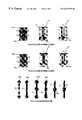
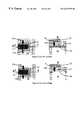
- FIG. 15 a-fis a series of plan views of trenches terminated with different-shaped condyles.
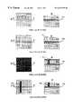
- a first trench etchcuts through the device layer at least as deep as the sacrificial material 10 b. As shown in FIG. 2, the first trench etch results in trench 11 and may be performed using a reactive-ion etch (RIE), for example. Trench 11 is then lined with an insulating material 12 , such as Low-Pressure Chemical-Vapor Deposition (LPCVD) silicon nitride, shown in FIG. 3 . The insulating material 12 may be used to completely fill the trench 11 or additional filler materials, such as silicon dioxide or polysilicon, may be used to complete the fill of trench 11 . Referring to FIG. 4, once the trench 11 has been filled, the trench fill material 12 is removed from the surface of the wafer to reveal the surface of the substrate 10 a.
- RIEreactive-ion etch
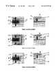
- isolation trenches 20and by removal of sacrificial material 10 b as shown in FIG. 7 .
- Sacrificial material 10 bmay be removed with a wet-release process.
- the sacrificial material 10 bis silicon dioxide any of a number of well known etching chemistries, including hydrofluoric acid, may be used to remove sacrificial material under structures 21 as well as remove sacrificial material exposed by open regions 25 .
- removing sacrificial material under structures 21leaves open areas 26 , mechanically freeing structures from the handle wafer.
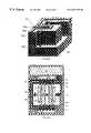
- a perspective view of a very simple microfabricated deviceis shown in FIG. 8 .
Landscapes
- Engineering & Computer Science (AREA)
- Physics & Mathematics (AREA)
- General Physics & Mathematics (AREA)
- Manufacturing & Machinery (AREA)
- Microelectronics & Electronic Packaging (AREA)
- Pressure Sensors (AREA)
Abstract
Description
Claims (17)
Priority Applications (1)
| Application Number | Priority Date | Filing Date | Title |
|---|---|---|---|
| US09/322,381US6291875B1 (en) | 1998-06-24 | 1999-05-28 | Microfabricated structures with electrical isolation and interconnections |
Applications Claiming Priority (2)
| Application Number | Priority Date | Filing Date | Title |
|---|---|---|---|
| US9051998P | 1998-06-24 | 1998-06-24 | |
| US09/322,381US6291875B1 (en) | 1998-06-24 | 1999-05-28 | Microfabricated structures with electrical isolation and interconnections |
Publications (1)
| Publication Number | Publication Date |
|---|---|
| US6291875B1true US6291875B1 (en) | 2001-09-18 |
Family
ID=26782363
Family Applications (1)
| Application Number | Title | Priority Date | Filing Date |
|---|---|---|---|
| US09/322,381Expired - LifetimeUS6291875B1 (en) | 1998-06-24 | 1999-05-28 | Microfabricated structures with electrical isolation and interconnections |
Country Status (1)
| Country | Link |
|---|---|
| US (1) | US6291875B1 (en) |
Cited By (63)
| Publication number | Priority date | Publication date | Assignee | Title |
|---|---|---|---|---|
| US6413793B1 (en)* | 2001-05-17 | 2002-07-02 | Xerox Corporation | Method of forming protrusions on single crystal silicon structures built on silicon-on-insulator wafers |
| US20020119597A1 (en)* | 2001-01-30 | 2002-08-29 | Stmicroelectronics S.R.L. | Process for sealing and connecting parts of electromechanical, fluid and optical microsystems and device obtained thereby |
| US6583374B2 (en)* | 2001-02-20 | 2003-06-24 | Rockwell Automation Technologies, Inc. | Microelectromechanical system (MEMS) digital electrical isolator |
| US6611168B1 (en) | 2001-12-19 | 2003-08-26 | Analog Devices, Inc. | Differential parametric amplifier with physically-coupled electrically-isolated micromachined structures |
| WO2003037782A3 (en)* | 2001-10-20 | 2004-01-29 | Bosch Gmbh Robert | Micromechanical component and method for producing same |
| US20040102021A1 (en)* | 2001-01-02 | 2004-05-27 | Sawyer William D. | Method for microfabricating structures using silicon-on-insulator material |
| US6868726B2 (en)* | 2000-01-20 | 2005-03-22 | Analog Devices Imi, Inc. | Position sensing with improved linearity |
| US6879016B1 (en) | 2002-10-07 | 2005-04-12 | Zyvex Corporation | Microcomponent having intra-layer electrical isolation with mechanical robustness |
| US6887391B1 (en)* | 2000-03-24 | 2005-05-03 | Analog Devices, Inc. | Fabrication and controlled release of structures using etch-stop trenches |
| WO2004017371A3 (en)* | 2002-08-15 | 2005-08-18 | Draper Lab Charles S | Method for microfabricating structures using silicon-on-insulator material |
| US6936491B2 (en) | 2003-06-04 | 2005-08-30 | Robert Bosch Gmbh | Method of fabricating microelectromechanical systems and devices having trench isolated contacts |
| US6952041B2 (en) | 2003-07-25 | 2005-10-04 | Robert Bosch Gmbh | Anchors for microelectromechanical systems having an SOI substrate, and method of fabricating same |
| US6973829B2 (en)* | 2000-08-29 | 2005-12-13 | Denso Corporation | Semiconductor dynamic quantity sensor with movable electrode and fixed electrode supported by support substrate |
| US20050287760A1 (en)* | 2004-06-29 | 2005-12-29 | Peking University | Method for fabricating high aspect ratio MEMS device with integrated circuit on the same substrate using post-CMOS process |
| US20060076640A1 (en)* | 2004-07-30 | 2006-04-13 | Zetex Plc | Semiconductor device |
| WO2006060937A1 (en)* | 2004-12-10 | 2006-06-15 | Shanghai Institute Of Microsystem And Information Technology, Chinese Academy Of Sciences | A mems device including a laterally movable portion wiht piezo-resistive sensing elements and electrostatic actuating elements on trench side walls and methods for producing the same |
| US7068125B2 (en) | 2004-03-04 | 2006-06-27 | Robert Bosch Gmbh | Temperature controlled MEMS resonator and method for controlling resonator frequency |
| US7075160B2 (en) | 2003-06-04 | 2006-07-11 | Robert Bosch Gmbh | Microelectromechanical systems and devices having thin film encapsulated mechanical structures |
| US7102467B2 (en) | 2004-04-28 | 2006-09-05 | Robert Bosch Gmbh | Method for adjusting the frequency of a MEMS resonator |
| US20070029629A1 (en)* | 2005-07-21 | 2007-02-08 | Evigia Systems, Inc. | Integrated sensor and circuitry and process therefor |
| US20070096249A1 (en)* | 2005-08-31 | 2007-05-03 | Heiko Roeper | Three-dimensionally integrated electronic assembly |
| US7224035B1 (en) | 2002-10-07 | 2007-05-29 | Zyvex Corporation | Apparatus and fabrication methods for incorporating sub-millimeter, high-resistivity mechanical components with low-resistivity conductors while maintaining electrical isolation therebetween |
| US20070180912A1 (en)* | 2002-07-19 | 2007-08-09 | Analog Devices, Inc. | Inertial sensor |
| US20070193355A1 (en)* | 2006-02-21 | 2007-08-23 | Physical Logic Ag | Accelerometer |
| US20080003779A1 (en)* | 2001-01-02 | 2008-01-03 | The Charles Stark Draper Laboratory, Inc. | Mems device and interposer and method for integrating mems device and interposer |
| US20080006889A1 (en)* | 2006-06-05 | 2008-01-10 | Akustica, Inc. | Monolithic MEMS and integrated circuit device having a barrier and method of fabricating the same |
| US20080042224A1 (en)* | 2004-05-08 | 2008-02-21 | X-Fab Semiconductor Foundries Ag | Soi Disks Comprising Mems Structures and Filled Isolating Trenches Having a Defined Cross-Section |
| US7514283B2 (en) | 2003-03-20 | 2009-04-07 | Robert Bosch Gmbh | Method of fabricating electromechanical device having a controlled atmosphere |
| US7795695B2 (en) | 2005-01-27 | 2010-09-14 | Analog Devices, Inc. | Integrated microphone |
| US20120074583A1 (en)* | 2010-09-28 | 2012-03-29 | Dao Thuy B | Semiconductor structure having a through substrate via (tsv) and method for forming |
| WO2012067850A1 (en)* | 2010-11-15 | 2012-05-24 | DigitalOptics Corporation MEMS | Mounting flexure contacts |
| US20120205752A1 (en)* | 2011-02-14 | 2012-08-16 | Kionix, Inc. | Strengthened Micro-Electromechanical System Devices and Methods of Making Thereof |
| US8430580B2 (en) | 2010-11-15 | 2013-04-30 | DigitalOptics Corporation MEMS | Rotationally deployed actuators |
| US8521017B2 (en) | 2010-11-15 | 2013-08-27 | DigitalOptics Corporation MEMS | MEMS actuator alignment |
| US8547627B2 (en) | 2010-11-15 | 2013-10-01 | DigitalOptics Corporation MEMS | Electrical routing |
| US8604663B2 (en) | 2010-11-15 | 2013-12-10 | DigitalOptics Corporation MEMS | Motion controlled actuator |
| US8608393B2 (en) | 2010-11-15 | 2013-12-17 | DigitalOptics Corporation MEMS | Capillary actuator deployment |
| US8616791B2 (en) | 2011-09-28 | 2013-12-31 | DigitalOptics Corporation MEMS | Rotationally deployed actuator devices |
| US8619378B2 (en) | 2010-11-15 | 2013-12-31 | DigitalOptics Corporation MEMS | Rotational comb drive Z-stage |
| US8624349B1 (en)* | 2010-10-11 | 2014-01-07 | Maxim Integrated Products, Inc. | Simultaneous isolation trench and handle wafer contact formation |
| US8637961B2 (en) | 2010-11-15 | 2014-01-28 | DigitalOptics Corporation MEMS | MEMS actuator device |
| US8695426B2 (en) | 2010-12-23 | 2014-04-15 | Industrial Technology Research Institute | Micro-electromechanical system device having electrical insulating structure and manufacturing methods |
| US8768157B2 (en) | 2011-09-28 | 2014-07-01 | DigitalOptics Corporation MEMS | Multiple degree of freedom actuator |
| US8803256B2 (en) | 2010-11-15 | 2014-08-12 | DigitalOptics Corporation MEMS | Linearly deployed actuators |
| US8855476B2 (en) | 2011-09-28 | 2014-10-07 | DigitalOptics Corporation MEMS | MEMS-based optical image stabilization |
| US8871551B2 (en) | 2006-01-20 | 2014-10-28 | Sitime Corporation | Wafer encapsulated microelectromechanical structure and method of manufacturing same |
| US8884381B2 (en) | 2010-11-15 | 2014-11-11 | DigitalOptics Corporation MEMS | Guard trench |
| US8941192B2 (en) | 2010-11-15 | 2015-01-27 | DigitalOptics Corporation MEMS | MEMS actuator device deployment |
| US9000556B2 (en) | 2011-10-07 | 2015-04-07 | International Business Machines Corporation | Lateral etch stop for NEMS release etch for high density NEMS/CMOS monolithic integration |
| US9019390B2 (en) | 2011-09-28 | 2015-04-28 | DigitalOptics Corporation MEMS | Optical image stabilization using tangentially actuated MEMS devices |
| US9052567B2 (en) | 2010-11-15 | 2015-06-09 | DigitalOptics Corporation MEMS | Actuator inside of motion control |
| US9061883B2 (en) | 2010-11-15 | 2015-06-23 | DigitalOptics Corporation MEMS | Actuator motion control features |
| US9063278B2 (en) | 2010-11-15 | 2015-06-23 | DigitalOptics Corporation MEMS | Miniature MEMS actuator assemblies |
| US9079763B2 (en) | 2013-04-22 | 2015-07-14 | Freescale Semiconductor, Inc. | MEMS device with stress isolation and method of fabrication |
| WO2015128062A1 (en)* | 2014-02-25 | 2015-09-03 | Northrop Grumman Litef Gmbh | Micromechanical component having a split, galvanically isolated active structure, and method for operating such a component |
| US9136157B1 (en)* | 2003-04-09 | 2015-09-15 | Newport Fab, Llc | Deep N wells in triple well structures |
| US9352962B2 (en) | 2010-11-15 | 2016-05-31 | DigitalOptics Corporation MEMS | MEMS isolation structures |
| US9515579B2 (en) | 2010-11-15 | 2016-12-06 | Digitaloptics Corporation | MEMS electrical contact systems and methods |
| DE102020210597A1 (en) | 2020-08-20 | 2022-02-24 | Robert Bosch Gesellschaft mit beschränkter Haftung | Method for manufacturing a microelectromechanical structure and microelectromechanical structure |
| US11358858B2 (en)* | 2020-01-24 | 2022-06-14 | Panasonic Intellectual Property Management Co., Ltd. | Semiconductor device and method of manufacturing thereof |
| DE102020215619A1 (en) | 2020-12-10 | 2022-06-15 | Robert Bosch Gesellschaft mit beschränkter Haftung | Process for fabricating vertically separated electrically isolated micromechanical structures and micromechanical device |
| DE102014008026B4 (en) | 2013-05-31 | 2023-03-16 | Stmicroelectronics S.R.L. | Integrated vacuum microelectronic device and method of making the same |
| DE102023203688A1 (en)* | 2023-04-21 | 2024-10-24 | Robert Bosch Gesellschaft mit beschränkter Haftung | Micromechanical device |
Citations (29)
| Publication number | Priority date | Publication date | Assignee | Title |
|---|---|---|---|---|
| US5084408A (en) | 1989-10-16 | 1992-01-28 | Kabushiki Kaisha Toshiba | Method of making complete dielectric isolation structure in semiconductor integrated circuit |
| US5198390A (en) | 1992-01-16 | 1993-03-30 | Cornell Research Foundation, Inc. | RIE process for fabricating submicron, silicon electromechanical structures |
| US5326726A (en) | 1990-08-17 | 1994-07-05 | Analog Devices, Inc. | Method for fabricating monolithic chip containing integrated circuitry and suspended microstructure |
| US5343064A (en) | 1988-03-18 | 1994-08-30 | Spangler Leland J | Fully integrated single-crystal silicon-on-insulator process, sensors and circuits |
| US5445988A (en) | 1993-07-13 | 1995-08-29 | Siemens Aktiengesellschaft | Method for manufacturing a trench in a substrate for use in smart-power technology |
| US5447067A (en) | 1993-03-30 | 1995-09-05 | Siemens Aktiengesellschaft | Acceleration sensor and method for manufacturing same |
| US5495761A (en) | 1992-12-28 | 1996-03-05 | Commissariat A L'energie Atomique | Integrated accelerometer with a sensitive axis parallel to the substrate |
| US5504026A (en) | 1995-04-14 | 1996-04-02 | Analog Devices, Inc. | Methods for planarization and encapsulation of micromechanical devices in semiconductor processes |
| US5506175A (en) | 1993-06-01 | 1996-04-09 | Cornell Research Foundation, Inc. | Method of forming compound stage MEM actuator suspended for multidimensional motion |
| US5569852A (en) | 1994-01-05 | 1996-10-29 | Robert Bosch Gmbh | Capacitive accelerometer sensor and method for its manufacture |
| US5574222A (en) | 1994-09-02 | 1996-11-12 | Robert Bosch Gmbh | Acceleration sensor |
| US5576250A (en) | 1992-12-28 | 1996-11-19 | Commissariat A L'energie Atomique | Process for the production of accelerometers using silicon on insulator technology |
| US5578755A (en) | 1993-12-03 | 1996-11-26 | Robert Bosch Gmbh | Accelerometer sensor of crystalline material and method for manufacturing the same |
| US5592015A (en) | 1993-03-10 | 1997-01-07 | Nippondenso Co., Ltd. | Dielectric isolated type semiconductor device provided with bipolar element |
| US5616523A (en) | 1993-05-06 | 1997-04-01 | Robert Bosch Gmbh | Method of manufacturing sensor |
| US5627318A (en) | 1992-08-21 | 1997-05-06 | Nippondenso Co., Ltd. | Mechanical force sensing semiconductor device |
| US5627317A (en) | 1994-06-07 | 1997-05-06 | Robert Bosch Gmbh | Acceleration sensor |
| US5631422A (en) | 1995-02-02 | 1997-05-20 | Robert Bosch Gmbh | Sensor comprising multilayer substrate |
| US5719073A (en) | 1993-02-04 | 1998-02-17 | Cornell Research Foundation, Inc. | Microstructures and single mask, single-crystal process for fabrication thereof |
| US5723353A (en) | 1995-02-10 | 1998-03-03 | Robert Bosch Gmbh | Process for manufacturing a sensor |
| US5747867A (en) | 1995-01-09 | 1998-05-05 | Siemens Aktiengesellschaft | Integrated circuit structure with interconnect formed along walls of silicon island |
| US5747353A (en) | 1996-04-16 | 1998-05-05 | National Semiconductor Corporation | Method of making surface micro-machined accelerometer using silicon-on-insulator technology |
| US5756901A (en) | 1995-10-11 | 1998-05-26 | Robert Bosch Gmbh | Sensor and method for manufacturing a sensor |
| US5798283A (en) | 1995-09-06 | 1998-08-25 | Sandia Corporation | Method for integrating microelectromechanical devices with electronic circuitry |
| US5847280A (en) | 1990-08-17 | 1998-12-08 | Analog Devices, Inc. | Monolithic micromechanical apparatus with suspended microstructure |
| US5882532A (en) | 1996-05-31 | 1999-03-16 | Hewlett-Packard Company | Fabrication of single-crystal silicon structures using sacrificial-layer wafer bonding |
| US6067858A (en)* | 1996-05-31 | 2000-05-30 | The Regents Of The University Of California | Micromachined vibratory rate gyroscope |
| US6180536B1 (en)* | 1998-06-04 | 2001-01-30 | Cornell Research Foundation, Inc. | Suspended moving channels and channel actuators for microfluidic applications and method for making |
| US6199874B1 (en)* | 1993-05-26 | 2001-03-13 | Cornell Research Foundation Inc. | Microelectromechanical accelerometer for automotive applications |
- 1999
- 1999-05-28USUS09/322,381patent/US6291875B1/ennot_activeExpired - Lifetime
Patent Citations (31)
| Publication number | Priority date | Publication date | Assignee | Title |
|---|---|---|---|---|
| US5343064A (en) | 1988-03-18 | 1994-08-30 | Spangler Leland J | Fully integrated single-crystal silicon-on-insulator process, sensors and circuits |
| US5084408A (en) | 1989-10-16 | 1992-01-28 | Kabushiki Kaisha Toshiba | Method of making complete dielectric isolation structure in semiconductor integrated circuit |
| US5326726A (en) | 1990-08-17 | 1994-07-05 | Analog Devices, Inc. | Method for fabricating monolithic chip containing integrated circuitry and suspended microstructure |
| US5847280A (en) | 1990-08-17 | 1998-12-08 | Analog Devices, Inc. | Monolithic micromechanical apparatus with suspended microstructure |
| US5198390A (en) | 1992-01-16 | 1993-03-30 | Cornell Research Foundation, Inc. | RIE process for fabricating submicron, silicon electromechanical structures |
| US5627318A (en) | 1992-08-21 | 1997-05-06 | Nippondenso Co., Ltd. | Mechanical force sensing semiconductor device |
| US5576250A (en) | 1992-12-28 | 1996-11-19 | Commissariat A L'energie Atomique | Process for the production of accelerometers using silicon on insulator technology |
| US5495761A (en) | 1992-12-28 | 1996-03-05 | Commissariat A L'energie Atomique | Integrated accelerometer with a sensitive axis parallel to the substrate |
| US5719073A (en) | 1993-02-04 | 1998-02-17 | Cornell Research Foundation, Inc. | Microstructures and single mask, single-crystal process for fabrication thereof |
| US5847454A (en) | 1993-02-04 | 1998-12-08 | Cornell Research Foundcatton, Inc. | Electrically isolated released microstructures |
| US5592015A (en) | 1993-03-10 | 1997-01-07 | Nippondenso Co., Ltd. | Dielectric isolated type semiconductor device provided with bipolar element |
| US5447067A (en) | 1993-03-30 | 1995-09-05 | Siemens Aktiengesellschaft | Acceleration sensor and method for manufacturing same |
| US5616523A (en) | 1993-05-06 | 1997-04-01 | Robert Bosch Gmbh | Method of manufacturing sensor |
| US6199874B1 (en)* | 1993-05-26 | 2001-03-13 | Cornell Research Foundation Inc. | Microelectromechanical accelerometer for automotive applications |
| US5506175A (en) | 1993-06-01 | 1996-04-09 | Cornell Research Foundation, Inc. | Method of forming compound stage MEM actuator suspended for multidimensional motion |
| US5445988A (en) | 1993-07-13 | 1995-08-29 | Siemens Aktiengesellschaft | Method for manufacturing a trench in a substrate for use in smart-power technology |
| US5578755A (en) | 1993-12-03 | 1996-11-26 | Robert Bosch Gmbh | Accelerometer sensor of crystalline material and method for manufacturing the same |
| US5569852A (en) | 1994-01-05 | 1996-10-29 | Robert Bosch Gmbh | Capacitive accelerometer sensor and method for its manufacture |
| US5627317A (en) | 1994-06-07 | 1997-05-06 | Robert Bosch Gmbh | Acceleration sensor |
| US5574222A (en) | 1994-09-02 | 1996-11-12 | Robert Bosch Gmbh | Acceleration sensor |
| US5747867A (en) | 1995-01-09 | 1998-05-05 | Siemens Aktiengesellschaft | Integrated circuit structure with interconnect formed along walls of silicon island |
| US5631422A (en) | 1995-02-02 | 1997-05-20 | Robert Bosch Gmbh | Sensor comprising multilayer substrate |
| US5959208A (en) | 1995-02-08 | 1999-09-28 | Robert Bosch GmbH | Acceleration sensor |
| US5723353A (en) | 1995-02-10 | 1998-03-03 | Robert Bosch Gmbh | Process for manufacturing a sensor |
| US5504026A (en) | 1995-04-14 | 1996-04-02 | Analog Devices, Inc. | Methods for planarization and encapsulation of micromechanical devices in semiconductor processes |
| US5798283A (en) | 1995-09-06 | 1998-08-25 | Sandia Corporation | Method for integrating microelectromechanical devices with electronic circuitry |
| US5756901A (en) | 1995-10-11 | 1998-05-26 | Robert Bosch Gmbh | Sensor and method for manufacturing a sensor |
| US5747353A (en) | 1996-04-16 | 1998-05-05 | National Semiconductor Corporation | Method of making surface micro-machined accelerometer using silicon-on-insulator technology |
| US5882532A (en) | 1996-05-31 | 1999-03-16 | Hewlett-Packard Company | Fabrication of single-crystal silicon structures using sacrificial-layer wafer bonding |
| US6067858A (en)* | 1996-05-31 | 2000-05-30 | The Regents Of The University Of California | Micromachined vibratory rate gyroscope |
| US6180536B1 (en)* | 1998-06-04 | 2001-01-30 | Cornell Research Foundation, Inc. | Suspended moving channels and channel actuators for microfluidic applications and method for making |
Non-Patent Citations (4)
| Title |
|---|
| Brosnihan, T. et al., "Enbedded Interconnect and Electrical Isolation for High-Aspect-Ratio, SOI Inertial Instruments", Proc. 1997 International Conference on Solid-State Sensors and Actuators, Chicago, IL, pp. 637-640, Jun. 16-19, 1997. |
| Keller, Christopher, Microfabricated Silicon High Aspect Ratio Flexures for In-Plane Motion, Doctoral Dissertation University of California, 1998. |
| Sridhar, U. et al., "Isolation Process for Surface Micromachined Sensors and Actuators," iMEMS '97 International MEMS Workshop, National University of Singapore, Singapore, Dec., 1997. |
| U.S. application No. 08/874,568, Brosnihan et al., filed Jun. 13, 1997. |
Cited By (121)
| Publication number | Priority date | Publication date | Assignee | Title |
|---|---|---|---|---|
| US6868726B2 (en)* | 2000-01-20 | 2005-03-22 | Analog Devices Imi, Inc. | Position sensing with improved linearity |
| US6887391B1 (en)* | 2000-03-24 | 2005-05-03 | Analog Devices, Inc. | Fabrication and controlled release of structures using etch-stop trenches |
| US6973829B2 (en)* | 2000-08-29 | 2005-12-13 | Denso Corporation | Semiconductor dynamic quantity sensor with movable electrode and fixed electrode supported by support substrate |
| US20110001198A1 (en)* | 2001-01-02 | 2011-01-06 | Sawyer William D | Mems device and interposer and method for integrating mems device and interposer |
| US7335527B2 (en) | 2001-01-02 | 2008-02-26 | Sawyer William D | Method for microfabricating structures using silicon-on-insulator material |
| US20040102021A1 (en)* | 2001-01-02 | 2004-05-27 | Sawyer William D. | Method for microfabricating structures using silicon-on-insulator material |
| US20080003779A1 (en)* | 2001-01-02 | 2008-01-03 | The Charles Stark Draper Laboratory, Inc. | Mems device and interposer and method for integrating mems device and interposer |
| US7655538B2 (en) | 2001-01-02 | 2010-02-02 | The Charles Stark Draper Laboratory, Inc. | MEMS device and interposer and method for integrating MEMS device and interposer |
| US8809135B2 (en) | 2001-01-02 | 2014-08-19 | The Charles Stark Draper Laboratory, Inc. | MEMS device and interposer and method for integrating MEMS device and interposer |
| US6946314B2 (en)* | 2001-01-02 | 2005-09-20 | The Charles Stark Draper Laboratory, Inc. | Method for microfabricating structures using silicon-on-insulator material |
| US20060014358A1 (en)* | 2001-01-02 | 2006-01-19 | Sawyer William D | Method for microfabricating structures using silicon-on-insulator material |
| US7531897B2 (en)* | 2001-01-30 | 2009-05-12 | Stmicroelectronics S.R.L. | Process for sealing and connecting parts of electromechanical, fluid and optical microsystems and device obtained thereby |
| US20090186447A1 (en)* | 2001-01-30 | 2009-07-23 | Stmicroelectronics S.R.I. | Process for sealing and connecting parts of electromechanical, fluid and optical microsystems and device obtained thereby |
| US8050011B2 (en) | 2001-01-30 | 2011-11-01 | Stmicroelectronics S.R.L. | Process for sealing and connecting parts of electromechanical, fluid and optical microsystems and device obtained thereby |
| US20020119597A1 (en)* | 2001-01-30 | 2002-08-29 | Stmicroelectronics S.R.L. | Process for sealing and connecting parts of electromechanical, fluid and optical microsystems and device obtained thereby |
| US6583374B2 (en)* | 2001-02-20 | 2003-06-24 | Rockwell Automation Technologies, Inc. | Microelectromechanical system (MEMS) digital electrical isolator |
| US6413793B1 (en)* | 2001-05-17 | 2002-07-02 | Xerox Corporation | Method of forming protrusions on single crystal silicon structures built on silicon-on-insulator wafers |
| WO2003037782A3 (en)* | 2001-10-20 | 2004-01-29 | Bosch Gmbh Robert | Micromechanical component and method for producing same |
| US7312553B2 (en) | 2001-10-20 | 2007-12-25 | Robert Bosch Gmbh | Micromechanical component and method for producing same |
| US20050052092A1 (en)* | 2001-10-20 | 2005-03-10 | Franz Laermer | Micromechanical component and method for producing same |
| US6611168B1 (en) | 2001-12-19 | 2003-08-26 | Analog Devices, Inc. | Differential parametric amplifier with physically-coupled electrically-isolated micromachined structures |
| US7363816B2 (en) | 2002-07-19 | 2008-04-29 | Analog Devices, Inc. | Inertial sensor |
| CN100523821C (en)* | 2002-07-19 | 2009-08-05 | 模拟设备公司 | Accelerometer and method for reducing offset in accelerometer |
| US20070180912A1 (en)* | 2002-07-19 | 2007-08-09 | Analog Devices, Inc. | Inertial sensor |
| AU2003272215B2 (en)* | 2002-08-15 | 2009-09-10 | The Charles Stark Draper Laboratory, Inc | Method for microfabricating structures using silicon-on-insulator material |
| WO2004017371A3 (en)* | 2002-08-15 | 2005-08-18 | Draper Lab Charles S | Method for microfabricating structures using silicon-on-insulator material |
| US7224035B1 (en) | 2002-10-07 | 2007-05-29 | Zyvex Corporation | Apparatus and fabrication methods for incorporating sub-millimeter, high-resistivity mechanical components with low-resistivity conductors while maintaining electrical isolation therebetween |
| US6879016B1 (en) | 2002-10-07 | 2005-04-12 | Zyvex Corporation | Microcomponent having intra-layer electrical isolation with mechanical robustness |
| US7514283B2 (en) | 2003-03-20 | 2009-04-07 | Robert Bosch Gmbh | Method of fabricating electromechanical device having a controlled atmosphere |
| US9136157B1 (en)* | 2003-04-09 | 2015-09-15 | Newport Fab, Llc | Deep N wells in triple well structures |
| US7352040B2 (en) | 2003-06-04 | 2008-04-01 | Robert Bosch Gmbh | Microelectromechanical systems having trench isolated contacts, and methods for fabricating same |
| US7288824B2 (en) | 2003-06-04 | 2007-10-30 | Robert Bosch Gmbh | Microelectromechanical systems, and devices having thin film encapsulated mechanical structures |
| US7075160B2 (en) | 2003-06-04 | 2006-07-11 | Robert Bosch Gmbh | Microelectromechanical systems and devices having thin film encapsulated mechanical structures |
| US8421167B2 (en) | 2003-06-04 | 2013-04-16 | Robert Bosch Gmbh | Microelectromechanical device including an encapsulation layer of which a portion is removed to expose a substantially planar surface having a portion that is disposed outside and above a chamber and including a field region on which integrated circuits are formed, and methods for fabricating same |
| US6936491B2 (en) | 2003-06-04 | 2005-08-30 | Robert Bosch Gmbh | Method of fabricating microelectromechanical systems and devices having trench isolated contacts |
| US7859067B2 (en) | 2003-06-04 | 2010-12-28 | Robert Bosch Gmbh | Microelectromechanical device including an encapsulation layer of which a portion is removed to expose a substantially planar surface having a portion that is disposed outside and above a chamber and including a field region on which integrated circuits are formed and methods for fabricating same |
| US8623686B2 (en) | 2003-06-04 | 2014-01-07 | Robert Bosch Gmbh | Microelectromechanical device including an encapsulation layer of which a portion is removed to expose a substantially planar surface having a portion that is disposed outside and above a chamber and including a field region on which integrated circuits are formed, and methods for fabricating same |
| US6952041B2 (en) | 2003-07-25 | 2005-10-04 | Robert Bosch Gmbh | Anchors for microelectromechanical systems having an SOI substrate, and method of fabricating same |
| US7317233B2 (en) | 2003-07-25 | 2008-01-08 | Robert Bosch Gmbh | Anchors for microelectromechanical systems having an SOI substrate, and method of fabricating same |
| WO2005017972A3 (en)* | 2003-08-15 | 2005-09-09 | Draper Lab Charles S | Method for microfabricating structures using silicon-on-insulator material |
| US7427905B2 (en) | 2004-03-04 | 2008-09-23 | Robert Bosch Gmbh | Temperature controlled MEMS resonator and method for controlling resonator frequency |
| US7268646B2 (en) | 2004-03-04 | 2007-09-11 | Robert Bosch Gmbh | Temperature controlled MEMS resonator and method for controlling resonator frequency |
| US7068125B2 (en) | 2004-03-04 | 2006-06-27 | Robert Bosch Gmbh | Temperature controlled MEMS resonator and method for controlling resonator frequency |
| US7221241B2 (en) | 2004-04-28 | 2007-05-22 | Robert Bosch Gmbh | Method for adjusting the frequency of a MEMS resonator |
| US7102467B2 (en) | 2004-04-28 | 2006-09-05 | Robert Bosch Gmbh | Method for adjusting the frequency of a MEMS resonator |
| US8742536B2 (en)* | 2004-05-08 | 2014-06-03 | X-Fab Semiconductor Foundries Ag | SOI disks comprising MEMS structures and filled isolating trenches having a defined cross-section |
| US20080042224A1 (en)* | 2004-05-08 | 2008-02-21 | X-Fab Semiconductor Foundries Ag | Soi Disks Comprising Mems Structures and Filled Isolating Trenches Having a Defined Cross-Section |
| US7618837B2 (en) | 2004-06-29 | 2009-11-17 | Peking University | Method for fabricating high aspect ratio MEMS device with integrated circuit on the same substrate using post-CMOS process |
| US20050287760A1 (en)* | 2004-06-29 | 2005-12-29 | Peking University | Method for fabricating high aspect ratio MEMS device with integrated circuit on the same substrate using post-CMOS process |
| US20060076640A1 (en)* | 2004-07-30 | 2006-04-13 | Zetex Plc | Semiconductor device |
| WO2006060937A1 (en)* | 2004-12-10 | 2006-06-15 | Shanghai Institute Of Microsystem And Information Technology, Chinese Academy Of Sciences | A mems device including a laterally movable portion wiht piezo-resistive sensing elements and electrostatic actuating elements on trench side walls and methods for producing the same |
| US7795695B2 (en) | 2005-01-27 | 2010-09-14 | Analog Devices, Inc. | Integrated microphone |
| US20070029629A1 (en)* | 2005-07-21 | 2007-02-08 | Evigia Systems, Inc. | Integrated sensor and circuitry and process therefor |
| US7562573B2 (en)* | 2005-07-21 | 2009-07-21 | Evigia Systems, Inc. | Integrated sensor and circuitry and process therefor |
| US7810394B2 (en) | 2005-07-21 | 2010-10-12 | Evigia Systems Inc. | Integrated sensor and circuitry |
| US20090140356A1 (en)* | 2005-07-21 | 2009-06-04 | Evigia Systems, Inc. | Integrated sensor and circuitry and process therefor |
| US20070096249A1 (en)* | 2005-08-31 | 2007-05-03 | Heiko Roeper | Three-dimensionally integrated electronic assembly |
| US10099917B2 (en) | 2006-01-20 | 2018-10-16 | Sitime Corporation | Encapsulated microelectromechanical structure |
| US9440845B2 (en) | 2006-01-20 | 2016-09-13 | Sitime Corporation | Encapsulated microelectromechanical structure |
| US10450190B2 (en) | 2006-01-20 | 2019-10-22 | Sitime Corporation | Encapsulated microelectromechanical structure |
| US11685650B2 (en) | 2006-01-20 | 2023-06-27 | Sitime Corporation | Microelectromechanical structure with bonded cover |
| US8871551B2 (en) | 2006-01-20 | 2014-10-28 | Sitime Corporation | Wafer encapsulated microelectromechanical structure and method of manufacturing same |
| US10766768B2 (en) | 2006-01-20 | 2020-09-08 | Sitime Corporation | Encapsulated microelectromechanical structure |
| US9434608B2 (en) | 2006-01-20 | 2016-09-06 | Sitime Corporation | Wafer encapsulated microelectromechanical structure |
| US9758371B2 (en) | 2006-01-20 | 2017-09-12 | Sitime Corporation | Encapsulated microelectromechanical structure |
| US20070193355A1 (en)* | 2006-02-21 | 2007-08-23 | Physical Logic Ag | Accelerometer |
| US7617729B2 (en)* | 2006-02-21 | 2009-11-17 | Physical Logic Ag | Accelerometer |
| US7863714B2 (en)* | 2006-06-05 | 2011-01-04 | Akustica, Inc. | Monolithic MEMS and integrated circuit device having a barrier and method of fabricating the same |
| TWI404169B (en)* | 2006-06-05 | 2013-08-01 | Akustica Inc | Integrated circuit device with barrier and manufacturing method thereof |
| US20080006889A1 (en)* | 2006-06-05 | 2008-01-10 | Akustica, Inc. | Monolithic MEMS and integrated circuit device having a barrier and method of fabricating the same |
| US8890324B2 (en)* | 2010-09-28 | 2014-11-18 | Freescale Semiconductor, Inc. | Semiconductor structure having a through substrate via (TSV) and method for forming |
| US20120074583A1 (en)* | 2010-09-28 | 2012-03-29 | Dao Thuy B | Semiconductor structure having a through substrate via (tsv) and method for forming |
| US8963281B1 (en) | 2010-10-11 | 2015-02-24 | Maxim Integrated Products, Inc. | Simultaneous isolation trench and handle wafer contact formation |
| US8624349B1 (en)* | 2010-10-11 | 2014-01-07 | Maxim Integrated Products, Inc. | Simultaneous isolation trench and handle wafer contact formation |
| US8430580B2 (en) | 2010-11-15 | 2013-04-30 | DigitalOptics Corporation MEMS | Rotationally deployed actuators |
| US8608393B2 (en) | 2010-11-15 | 2013-12-17 | DigitalOptics Corporation MEMS | Capillary actuator deployment |
| WO2012067850A1 (en)* | 2010-11-15 | 2012-05-24 | DigitalOptics Corporation MEMS | Mounting flexure contacts |
| US8521017B2 (en) | 2010-11-15 | 2013-08-27 | DigitalOptics Corporation MEMS | MEMS actuator alignment |
| US8803256B2 (en) | 2010-11-15 | 2014-08-12 | DigitalOptics Corporation MEMS | Linearly deployed actuators |
| US8637961B2 (en) | 2010-11-15 | 2014-01-28 | DigitalOptics Corporation MEMS | MEMS actuator device |
| US10003282B2 (en) | 2010-11-15 | 2018-06-19 | DigitalOptics Corporation MEMS | Linearly deployed actuators |
| US9899938B2 (en) | 2010-11-15 | 2018-02-20 | DigitalOptics Corporation MEMS | Miniature MEMS actuator assemblies |
| US8873174B2 (en) | 2010-11-15 | 2014-10-28 | DigitalOptics Corporation MEMS | Mounting flexure contacts |
| US8884381B2 (en) | 2010-11-15 | 2014-11-11 | DigitalOptics Corporation MEMS | Guard trench |
| US8619378B2 (en) | 2010-11-15 | 2013-12-31 | DigitalOptics Corporation MEMS | Rotational comb drive Z-stage |
| TWI464106B (en)* | 2010-11-15 | 2014-12-11 | Digitaloptics Corp Mems | Device, system and electronic device having a flexure, and method for forming a flexure |
| US8922870B2 (en) | 2010-11-15 | 2014-12-30 | DigitalOptics Corporation MEMS | Electrical routing |
| US8941192B2 (en) | 2010-11-15 | 2015-01-27 | DigitalOptics Corporation MEMS | MEMS actuator device deployment |
| US8953934B2 (en) | 2010-11-15 | 2015-02-10 | DigitalOptics Corporation MEMS | MEMS actuator alignment |
| US8547627B2 (en) | 2010-11-15 | 2013-10-01 | DigitalOptics Corporation MEMS | Electrical routing |
| US9611926B2 (en) | 2010-11-15 | 2017-04-04 | DigitalOptics Corporation MEMS | Motion controlled actuator |
| US9541815B2 (en) | 2010-11-15 | 2017-01-10 | DigitalOptics Corporation MEMS | Actuator for motion control in miniature cameras |
| US9052567B2 (en) | 2010-11-15 | 2015-06-09 | DigitalOptics Corporation MEMS | Actuator inside of motion control |
| US9061883B2 (en) | 2010-11-15 | 2015-06-23 | DigitalOptics Corporation MEMS | Actuator motion control features |
| US9063278B2 (en) | 2010-11-15 | 2015-06-23 | DigitalOptics Corporation MEMS | Miniature MEMS actuator assemblies |
| US9515579B2 (en) | 2010-11-15 | 2016-12-06 | Digitaloptics Corporation | MEMS electrical contact systems and methods |
| US8605375B2 (en) | 2010-11-15 | 2013-12-10 | DigitalOptics Corporation MEMS | Mounting flexure contacts |
| US8604663B2 (en) | 2010-11-15 | 2013-12-10 | DigitalOptics Corporation MEMS | Motion controlled actuator |
| US9166463B2 (en) | 2010-11-15 | 2015-10-20 | DigitalOptics Corporation MEMS | Linearly deployed actuators |
| US9352962B2 (en) | 2010-11-15 | 2016-05-31 | DigitalOptics Corporation MEMS | MEMS isolation structures |
| US8695426B2 (en) | 2010-12-23 | 2014-04-15 | Industrial Technology Research Institute | Micro-electromechanical system device having electrical insulating structure and manufacturing methods |
| KR20140010077A (en)* | 2011-02-14 | 2014-01-23 | 키오닉스, 인크. | Strengthened micro-electromechanical system devices and methods of making thereof |
| US8664731B2 (en)* | 2011-02-14 | 2014-03-04 | Kionix, Inc. | Strengthened micro-electromechanical system devices and methods of making thereof |
| US20120205752A1 (en)* | 2011-02-14 | 2012-08-16 | Kionix, Inc. | Strengthened Micro-Electromechanical System Devices and Methods of Making Thereof |
| WO2012112452A3 (en)* | 2011-02-14 | 2012-10-18 | Kionix, Inc. | Strengthened micro-electromechanical system devices and methods of making thereof |
| TWI616394B (en)* | 2011-02-14 | 2018-03-01 | 奇奧尼公司 | Strengthened micro-electromechanical system devices and methods of making thereof |
| US9664922B2 (en) | 2011-09-28 | 2017-05-30 | DigitalOptics Corporation MEMS | MEMS-based optical image stabilization |
| US8616791B2 (en) | 2011-09-28 | 2013-12-31 | DigitalOptics Corporation MEMS | Rotationally deployed actuator devices |
| US8855476B2 (en) | 2011-09-28 | 2014-10-07 | DigitalOptics Corporation MEMS | MEMS-based optical image stabilization |
| US8768157B2 (en) | 2011-09-28 | 2014-07-01 | DigitalOptics Corporation MEMS | Multiple degree of freedom actuator |
| US9019390B2 (en) | 2011-09-28 | 2015-04-28 | DigitalOptics Corporation MEMS | Optical image stabilization using tangentially actuated MEMS devices |
| US9000556B2 (en) | 2011-10-07 | 2015-04-07 | International Business Machines Corporation | Lateral etch stop for NEMS release etch for high density NEMS/CMOS monolithic integration |
| US9162877B2 (en) | 2011-10-07 | 2015-10-20 | Globalfoundries U.S. 2 Llc | Lateral etch stop for NEMS release etch for high density NEMS/CMOS monolithic integration |
| US9079763B2 (en) | 2013-04-22 | 2015-07-14 | Freescale Semiconductor, Inc. | MEMS device with stress isolation and method of fabrication |
| DE102014008026B4 (en) | 2013-05-31 | 2023-03-16 | Stmicroelectronics S.R.L. | Integrated vacuum microelectronic device and method of making the same |
| RU2653112C2 (en)* | 2014-02-25 | 2018-05-07 | Нортроп Грумман Литеф Гмбх | Micromechanical component with a separate, galvanic isolated active structure and an operating method of such a component |
| WO2015128062A1 (en)* | 2014-02-25 | 2015-09-03 | Northrop Grumman Litef Gmbh | Micromechanical component having a split, galvanically isolated active structure, and method for operating such a component |
| US11358858B2 (en)* | 2020-01-24 | 2022-06-14 | Panasonic Intellectual Property Management Co., Ltd. | Semiconductor device and method of manufacturing thereof |
| DE102020210597A1 (en) | 2020-08-20 | 2022-02-24 | Robert Bosch Gesellschaft mit beschränkter Haftung | Method for manufacturing a microelectromechanical structure and microelectromechanical structure |
| DE102020215619A1 (en) | 2020-12-10 | 2022-06-15 | Robert Bosch Gesellschaft mit beschränkter Haftung | Process for fabricating vertically separated electrically isolated micromechanical structures and micromechanical device |
| DE102023203688A1 (en)* | 2023-04-21 | 2024-10-24 | Robert Bosch Gesellschaft mit beschränkter Haftung | Micromechanical device |
Similar Documents
| Publication | Publication Date | Title |
|---|---|---|
| US6291875B1 (en) | Microfabricated structures with electrical isolation and interconnections | |
| US6433401B1 (en) | Microfabricated structures with trench-isolation using bonded-substrates and cavities | |
| US6960488B2 (en) | Method of fabricating a microfabricated high aspect ratio device with electrical isolation | |
| US7943525B2 (en) | Method of producing microelectromechanical device with isolated microstructures | |
| US6988408B2 (en) | Surface/bulk micromachined single-crystalline silicon micro-gyroscope | |
| EP2023151B1 (en) | Sensor with position-indepedent drive electrodes in multi-layer silicon on insulator substrate | |
| US8443670B2 (en) | 3-axis accelerometer with gap-closing capacitive electrodes | |
| US8227876B2 (en) | Single crystal silicon sensor with additional layer and method of producing the same | |
| JP5316479B2 (en) | Manufacturing method of semiconductor dynamic quantity sensor and semiconductor dynamic quantity sensor | |
| US7437933B2 (en) | Micro-electro-mechanical structure having electrically insulated regions and manufacturing process thereof | |
| US20010013630A1 (en) | Isolation in micromachined single crystal silicon using deep trench insulation | |
| US7026184B2 (en) | Method of fabricating microstructures and devices made therefrom | |
| JPH11183518A (en) | Manufacture of sensor provided with accelerometer and gyro, and sensor manufactured by the method | |
| US7618837B2 (en) | Method for fabricating high aspect ratio MEMS device with integrated circuit on the same substrate using post-CMOS process | |
| US7550358B2 (en) | MEMS device including a laterally movable portion with piezo-resistive sensing elements and electrostatic actuating elements on trench side walls, and methods for producing the same | |
| US7361523B2 (en) | Three-axis accelerometer | |
| Lee et al. | Surface/bulk micromachining (SBM) process and deep trench oxide isolation method for MEMS | |
| Sawyer et al. | SOI bonded wafer process for high precision MEMS inertial sensors | |
| Fedder | Integrated MEMS in conventional CMOS | |
| KR100332360B1 (en) | Micro Gyroscope Fabricated by Single-crystalline Silicon Micromachining Technology | |
| Clark et al. | Microfabricated structures with electrical isolation and interconnections | |
| FEDDER | Department of Electrical and Computer Engineering | |
| Li et al. | Novel silicon cap package technology for monolithic microinertial measurement unit |
Legal Events
| Date | Code | Title | Description |
|---|---|---|---|
| AS | Assignment | Owner name:INTEGRATED MICRO INSTRUMENTS, INC., CALIFORNIA Free format text:ASSIGNMENT OF ASSIGNORS INTEREST;ASSIGNORS:CLARK, WILLIAM A.;JUNEAU, THOR N.;ROESSIG, ALLEN W.;AND OTHERS;REEL/FRAME:010014/0441 Effective date:19990527 | |
| FEPP | Fee payment procedure | Free format text:ENTITY STATUS SET TO UNDISCOUNTED (ORIGINAL EVENT CODE: BIG.); ENTITY STATUS OF PATENT OWNER: LARGE ENTITY | |
| AS | Assignment | Owner name:INTEGRATED MICRO INSTRUMENTS, INC., CALIFORNIA Free format text:MERGER;ASSIGNOR:INTEGRATED MICRO INSTRUMENTS, INC.;REEL/FRAME:011547/0629 Effective date:20001215 | |
| AS | Assignment | Owner name:ANALOG DEVICES IMI, INC., CALIFORNIA Free format text:ASSIGNMENT OF ASSIGNORS INTEREST;ASSIGNOR:INTEGRATED MICRO INSTRUMENTS, INC.;REEL/FRAME:011859/0275 Effective date:20010326 | |
| STCF | Information on status: patent grant | Free format text:PATENTED CASE | |
| FPAY | Fee payment | Year of fee payment:4 | |
| FPAY | Fee payment | Year of fee payment:8 | |
| FPAY | Fee payment | Year of fee payment:12 |