US6291321B1 - Controlling threading dislocation densities in Ge on Si using graded GeSi layers and planarization - Google Patents
Controlling threading dislocation densities in Ge on Si using graded GeSi layers and planarizationDownload PDFInfo
- Publication number
- US6291321B1 US6291321B1US09/265,016US26501699AUS6291321B1US 6291321 B1US6291321 B1US 6291321B1US 26501699 AUS26501699 AUS 26501699AUS 6291321 B1US6291321 B1US 6291321B1
- Authority
- US
- United States
- Prior art keywords
- layer
- substrate
- providing
- graded
- sample
- Prior art date
- Legal status (The legal status is an assumption and is not a legal conclusion. Google has not performed a legal analysis and makes no representation as to the accuracy of the status listed.)
- Expired - Lifetime
Links
Images


Classifications
- H—ELECTRICITY
- H01—ELECTRIC ELEMENTS
- H01L—SEMICONDUCTOR DEVICES NOT COVERED BY CLASS H10
- H01L21/00—Processes or apparatus adapted for the manufacture or treatment of semiconductor or solid state devices or of parts thereof
- H01L21/02—Manufacture or treatment of semiconductor devices or of parts thereof
- H01L21/04—Manufacture or treatment of semiconductor devices or of parts thereof the devices having potential barriers, e.g. a PN junction, depletion layer or carrier concentration layer
- H01L21/18—Manufacture or treatment of semiconductor devices or of parts thereof the devices having potential barriers, e.g. a PN junction, depletion layer or carrier concentration layer the devices having semiconductor bodies comprising elements of Group IV of the Periodic Table or AIIIBV compounds with or without impurities, e.g. doping materials
- H01L21/20—Deposition of semiconductor materials on a substrate, e.g. epitaxial growth solid phase epitaxy
- H—ELECTRICITY
- H01—ELECTRIC ELEMENTS
- H01L—SEMICONDUCTOR DEVICES NOT COVERED BY CLASS H10
- H01L21/00—Processes or apparatus adapted for the manufacture or treatment of semiconductor or solid state devices or of parts thereof
- H01L21/02—Manufacture or treatment of semiconductor devices or of parts thereof
- H01L21/02104—Forming layers
- H01L21/02365—Forming inorganic semiconducting materials on a substrate
- H01L21/02436—Intermediate layers between substrates and deposited layers
- H01L21/02494—Structure
- H01L21/02496—Layer structure
- H01L21/02505—Layer structure consisting of more than two layers
- H—ELECTRICITY
- H01—ELECTRIC ELEMENTS
- H01L—SEMICONDUCTOR DEVICES NOT COVERED BY CLASS H10
- H01L21/00—Processes or apparatus adapted for the manufacture or treatment of semiconductor or solid state devices or of parts thereof
- H01L21/02—Manufacture or treatment of semiconductor devices or of parts thereof
- H01L21/02104—Forming layers
- H01L21/02365—Forming inorganic semiconducting materials on a substrate
- H01L21/02367—Substrates
- H01L21/0237—Materials
- H01L21/02373—Group 14 semiconducting materials
- H01L21/02381—Silicon, silicon germanium, germanium
- H—ELECTRICITY
- H01—ELECTRIC ELEMENTS
- H01L—SEMICONDUCTOR DEVICES NOT COVERED BY CLASS H10
- H01L21/00—Processes or apparatus adapted for the manufacture or treatment of semiconductor or solid state devices or of parts thereof
- H01L21/02—Manufacture or treatment of semiconductor devices or of parts thereof
- H01L21/02104—Forming layers
- H01L21/02365—Forming inorganic semiconducting materials on a substrate
- H01L21/02367—Substrates
- H01L21/02433—Crystal orientation
- H—ELECTRICITY
- H01—ELECTRIC ELEMENTS
- H01L—SEMICONDUCTOR DEVICES NOT COVERED BY CLASS H10
- H01L21/00—Processes or apparatus adapted for the manufacture or treatment of semiconductor or solid state devices or of parts thereof
- H01L21/02—Manufacture or treatment of semiconductor devices or of parts thereof
- H01L21/02104—Forming layers
- H01L21/02365—Forming inorganic semiconducting materials on a substrate
- H01L21/02436—Intermediate layers between substrates and deposited layers
- H01L21/02439—Materials
- H01L21/02441—Group 14 semiconducting materials
- H01L21/0245—Silicon, silicon germanium, germanium
- H—ELECTRICITY
- H01—ELECTRIC ELEMENTS
- H01L—SEMICONDUCTOR DEVICES NOT COVERED BY CLASS H10
- H01L21/00—Processes or apparatus adapted for the manufacture or treatment of semiconductor or solid state devices or of parts thereof
- H01L21/02—Manufacture or treatment of semiconductor devices or of parts thereof
- H01L21/02104—Forming layers
- H01L21/02365—Forming inorganic semiconducting materials on a substrate
- H01L21/02436—Intermediate layers between substrates and deposited layers
- H01L21/02494—Structure
- H01L21/02496—Layer structure
- H01L21/02502—Layer structure consisting of two layers
- H—ELECTRICITY
- H01—ELECTRIC ELEMENTS
- H01L—SEMICONDUCTOR DEVICES NOT COVERED BY CLASS H10
- H01L21/00—Processes or apparatus adapted for the manufacture or treatment of semiconductor or solid state devices or of parts thereof
- H01L21/02—Manufacture or treatment of semiconductor devices or of parts thereof
- H01L21/02104—Forming layers
- H01L21/02365—Forming inorganic semiconducting materials on a substrate
- H01L21/02436—Intermediate layers between substrates and deposited layers
- H01L21/02494—Structure
- H01L21/02496—Layer structure
- H01L21/0251—Graded layers
- H—ELECTRICITY
- H01—ELECTRIC ELEMENTS
- H01L—SEMICONDUCTOR DEVICES NOT COVERED BY CLASS H10
- H01L21/00—Processes or apparatus adapted for the manufacture or treatment of semiconductor or solid state devices or of parts thereof
- H01L21/02—Manufacture or treatment of semiconductor devices or of parts thereof
- H01L21/02104—Forming layers
- H01L21/02365—Forming inorganic semiconducting materials on a substrate
- H01L21/02518—Deposited layers
- H01L21/02521—Materials
- H01L21/02524—Group 14 semiconducting materials
- H01L21/02532—Silicon, silicon germanium, germanium
- Y—GENERAL TAGGING OF NEW TECHNOLOGICAL DEVELOPMENTS; GENERAL TAGGING OF CROSS-SECTIONAL TECHNOLOGIES SPANNING OVER SEVERAL SECTIONS OF THE IPC; TECHNICAL SUBJECTS COVERED BY FORMER USPC CROSS-REFERENCE ART COLLECTIONS [XRACs] AND DIGESTS
- Y10—TECHNICAL SUBJECTS COVERED BY FORMER USPC
- Y10S—TECHNICAL SUBJECTS COVERED BY FORMER USPC CROSS-REFERENCE ART COLLECTIONS [XRACs] AND DIGESTS
- Y10S438/00—Semiconductor device manufacturing: process
- Y10S438/933—Germanium or silicon or Ge-Si on III-V
Definitions
- the inventionrelates to a method of creating flat, crack-free low-dislocation-density mismatched semiconductor layers, and of controlling threading dislocation densities in Ge on Si using graded SiGe layers.
- relaxed graded GeSi buffershave been used as “substrates” for the growth of high electron mobility structures and for the integration of III-V devices on Si.
- the relaxed graded bufferintroduces a 4% lattice mismatch between Si and Ge gradually, resulting in a disperse, three-dimensional misfit dislocation network. Strain-relieving glide of threading dislocations is facilitated, preventing the accumlation of mismatch strain. Because threading dislocations present in the initial layers can also be used to relieve strain in subsequent layers, the nucleation of additional dislocations is suppressed as the graded layer growth progresses. However, a complication arises during thick grades to high Ge concentrations.
- the characteristic crosshatch surface roughness and the underlying strain fields of the misfit arraycan overlap, blocking threading dislocation glide and leading to dislocation pile-ups.
- the formation of these pile-upsnecessitates the nucleation of additional threading dislocations, as the trapped threading dislocations can no longer contribute to strain relief.
- Growth on offcut Si substrateshas been shown to improve surface morphology and decrease the number of pile-ups, but not eliminate them entirely. Therefore, an increase in threading dislocation density and the number of pile-ups is always observed as the thickness of graded layers increases.
- CMPchemical-mechanical polishing
- UHVCVDultra-high vacuum chemical vapor deposition
- one embodiment of the inventionprovides a semiconductor structure comprising a semiconductor substrate, at least one first crystalline epitaxial layer on the substrate, the first layer having a surface which is planarized, and at least one second crystalline epitaxial layer on the at least one first layer.
- a semiconductor structurecomprising a silicon substrate, and a GeSi graded region grown on the silicon substrate, compressive strain being incorporated in the graded region to offset the tensile strain that is incorporated during thermal processing.
- a semiconductor structurecomprising a semiconductor substrate, a first layer having a graded region grown on the substrate, compressive strain being incorporated in the graded region to offset the tensile strain that is incorporated during thermal processing, the first layer having a surface which is planarized, and a second layer provided on the first layer.
- a method of fabricating a semiconductor structurecomprising providing a semiconductor substrate, providing at least one first crystalline epitaxial layer on the substrate, and planarizing the surface of the first layer.
- FIG. 1is a flowchart of processing steps of an exemplary experiment in accordance with the invention
- FIG. 2is a table of growth parameters and characterization results of exemplary structure samples in accordance with the invention.
- FIG. 3is a schematic representation of structure and growth conditions for a semiconductor structure in accordance with the invention.
- FIG. 4is a cross-sectional XTEM image of the upper graded region and uniform Ge cap of the structure of the invention.
- FIGS. 5A and 5Bare Nomarski optical micrographs comparing the EPD of exemplary semiconductor structure samples, respectively.
- composition-graded GeSi layersare a viable means to relax GeSi alloys on Si for concentrations ⁇ 50%, there is a rise in threading dislocation density with continued grading. See, for example, U.S. patent application Ser. No. 08/806,741 filed by Fitzgerald et al., incorporated herein by reference.
- a final Ge layerhas a lower defect density than Ge grown directly on Si, the residual defect density is still too high for many applications ( 18 10 7 cm ⁇ 2 ), and the density is certainly greater than relaxed Ge 30 S 70 on Si using this method ( ⁇ 7 ⁇ 10 5 cm ⁇ 2 ).
- the grading rate for such defect densities in Ge 30 Si 70is 10% Ge per micron of thickness.
- the grading rateis decreased to 5% Ge per micron of thickness. From experience, a lower grading rate will lower the threading dislocation density. However, it was found that the threading dislocation density was nearly equivalent to the 10% Ge/micron grading rate, cracks developed due to the thermal mismatch strain, and many particles were found due to what is believed to be gas-phase nucleation of GeSi since germane cracks at much lower temperatures than silane.
- the major problems that need to be controlled in the semiconductor structureare the cracking and the threading dislocation density. Cracking is due to the fact that at 5% Ge per micron, the final thickness is very great, and upon cooling from the growth temperature, the thermal mismatch between the deposited layers and Si results in a tensile strain. When the tensile strain is great enough, cracking is the relaxation mechanism, especially if dislocation flow ceases at some temperature during cooling. However, lowering the threading dislocation density requires a greater thickness, since the slower grading rate reduces the threading dislocation density. Thus, it would appear that the removal of cracks and the presence of a low number of threading dislocations are incompatible goals.
- the inventiontherefore, applies a planarization step within the growth of the buffer layer to remove the roughness created by the dislocations introduced during relaxation; i.e., the process effectively removes the “history” of the surface by planarization, preventing the continued roughening and grooving of the surface that leads to dislocation blocking.
- a drastic effectis found: the rise in threading dislocation density as one continues to grade can be completely eliminated.
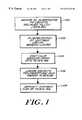
- FIG. 1is a flowchart of processing steps of an exemplary experiment in accordance with the invention. A summary of the exemplary experiment is as follows:
- a Si substrateis graded at 10% Ge per micron to Ge 50 Si 50 to create a relaxed alloy for exploring the growth at the high-Ge end which was problematic. This grading rate was not lowered since there was only a need to explore the high-Ge end. These layers were grown at 750° C. using UHVCVD. Defect analysis shows that a threading dislocation density on the order of 6 ⁇ 10 6 cm ⁇ 2 is achieved, exactly what was expected. Also, a number of dislocation pile-ups are found, which indicate that dislocation blocking has begun, but is not totally out of control.
- CMPchemo-mechanical polishing
- the wafersare inserted back into the UHVCVD system and grading is continued (i.e. regrowth) (step 104 ).
- Depositionis started at the Ge 50 Si 50 composition, and graded at 10% Ge per micron to 75% Ge, all at a growth temperature of 750° C.
- the growth temperatureis then lowered to 550° C. Then grading to 92% Ge occurs, at 10% Ge per micron (step 106 ).
- a uniform cap of pure Geis deposited, with 1-1.5 micron in thickness (step 108 ). This particular experiment has doping in the Ge cap so that Ge photodetectors can be fabricated.
- sample Awas graded from Si to 100% Ge at a rate of 5% Ge ⁇ m ⁇ 1 . It was grown at 750° C. and 25 mT and topped with a 3 ⁇ m Ge cap. A linear grade was approximted by increasing the Ge concentration in 2.5%, 5000 ⁇ steps.
- Sample Bwas graded to 100% Ge at a rate of 10% Ge ⁇ m ⁇ 1 , at a temperature of 800° C., and at a pressure of 50 mT. This structure corresponds to the sample structure from previous reports on the formation of dislocation pile-ups.
- Sample Cwas grown to only 50% Ge at a grading rate of 10% Ge ⁇ m ⁇ 1 and topped with a 1.5 ⁇ m 50% Ge cap. The graded region of sample C was composed of 2% Ge, 2000 ⁇ jumps.
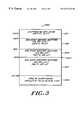
- FIG. 3is a schematic representation of structure and growth conditions for a semiconductor structure 300 (sample D) in accordance with the invention.
- the structure 300includes a (001) Si substrate 302 offcut 6° to in-plane ⁇ 110>.
- the structure 300was grown to include a relaxed graded buffer layer or region 304 of only 50% Ge at a grading rate of 10% Ge ⁇ m ⁇ 1 and topped with a 1.5 ⁇ m 50% Ge cap.
- the graded regionwas composed of 2% Ge, 2000 ⁇ jumps. To this point, the structure corresponds to sample C described heretofore.
- the top 5000 ⁇ of region 304was then removed via CMP, and a 50-100% Ge graded buffer region 306 was grown on top at a rate of 10% Ge ⁇ m ⁇ 1 , again in 2%, 2000 ⁇ steps.
- initiation of a second graded layeris accomplished by first growing a lattice-matched homoepitaxial uniform composition buffer layer before grading is initiated. In this 50-76% Ge portion, the growth conditions were held constant at 750° C. and 25 mT. Thereafter, the growth was halted and the temperature and pressure were lowered to 550° C. and 3 mT. The growth of a graded buffer region 308 then continued until a Ge concentration of 92% was reached. The final jump in Ge concentration was made from 92% to 100% and a 1.5 ⁇ m uniform cap layer 310 was deposited.
- FIG. 4is a cross-sectional transmission electron microscope (XTEM) micrograph of the upper graded region and the uniform cap of structure 300 (sample D). All of the samples in the study were grown on (100) Si wafers offcut 6° to the in-plane ⁇ 110> by UHVCVD.
- XTEMtransmission electron microscope
- the four sampleswere characterized via cross-sectional XTEM, plan view optical microscopy, etch-pit density (EPD), atomic force microscopy (APM), and triple-axis X-ray diffraction. The relevant results are presented in the table of FIG. 2 .
- the structure 300in effect a grade to 100% at 10% Ge ⁇ m ⁇ 1 , has a similar or even slightly lower threading dislocation density than the sample C—a lower value than that of both sample A and sample B.
- the addition of the CMP step at 50% Gehas arrested the increase in threading dislocation density with Ge concentration.
- the planarization of the surface during this stepmust free the threads seen in pile-ups in sample C, and allow the dislocations to relieve the stain introduced in the subsequent growth, eliminating the driving force for the nucleation of additional threading dislocations.
- FIGS. 5A and 5BNomarski optical micrographs comparing the EPD of samples C and D are shown in FIGS. 5A and 5B, respectively.
- the EPD resultsindicate threading dislocation densities in sample C, the 10% Ge ⁇ m ⁇ 1 grade to 50% Ge, and sample D, the 10% Ge ⁇ m ⁇ 1 grade to 100% Ge grown on sample B after a CMP planarization step.
- the threading dislocation densitiesare 6.3 ⁇ 0.1 ⁇ 10 6 cm ⁇ 2 for sample C, and 2.1 ⁇ 0.2 ⁇ 10 6 cm ⁇ 2 for sample D.
- Sample Bthe 10% Ge ⁇ m ⁇ 1 grade to 100% Ge, has the highest rms roughness, 47 nm.
- the high surface roughnessis due to the fast grading rate, creating the highest threading dislocation density of the four samples—well over 10 7 cm ⁇ 2 .
- the grading rateis decreased to 5% Ge ⁇ m ⁇ 1 for sample A, a corresponding decrease in surface roughness to 35.9 nm is observed. This roughness is on par with that of sample C and large enough to create pile-ups and increased threading dislocation density in both samples.
- sample Athe calculated strain due to thermal mismatch when cooling to room temperature is 2.6 ⁇ 10 ⁇ 3 , resulting in a high density of surface cracks.
- sample Dgrowth modifications specifically designed to alleviate this cracking problem are added.
- the fast grading rate at lower temperature and the final Ge concentration jump in sample Dfrom 92% to 100%, incorporate metastable compressive residual stress into the buffer at the growth temperature. Since the compressive lattice mismatch opposes the tensile thermal mismatch, sample D is left in a nearly stress-free state at room temperature.
- the X-ray diffraction dataindicates that the top layer is actually slightly compressive, preventing any surface cracking. Additionally, due to the large final jump in Ge concentration, the graded buffer of sample D has nearly 1 ⁇ m less Ge-rich material than sample B, decreasing its absolute value of strain energy from thermal mismatch stress. Hence, even though neither sample D nor sample B experienced surface cracking after growth, sample D will be the superior substrate for subsequent integration of III-V materials which are also thermally mismatched to Si. The lower growth temperature during the high Ge portion of sample D also decreased the amount of particulate contamination from gas phase nucleation events. These events occur much more frequently as the growth temperature and pressure increase, particularly near the melting point of the solid alloy.
- a 100% Ge graded bufferhas been grown at 10% Ge ⁇ m ⁇ 1 that exhibits a final threading dislocation density an order of magnitude lower than that of sample A, the 5% Ge ⁇ m ⁇ 1 grade with no planarization step. Additionally, the nucleation of threading dislocations in the 50-100% Ge portion of the growth has been suppressed through the release of immobile dislocations located in dislocation pile-ups. The surface morphology of the graded buffer has also been improved. Finally, surface cracking due to the thermal mismatch between Si and Ge and particles due to gas phase nucleation events have both been eliminated.
- the inventionthus provides a method of producing low threading dislocation density by using planarization steps within the graded buffer.
- the inventionessentially involves growing one lattice-mismatched semiconductor on another, planarizing the semiconductor growth, and regrowing a semiconductor on the polished surface, and continuing to grow a lattice-mismatched structure that continues to relax.
- the growth temperaturesare reduced at the high Ge end to balance the thermal expansion difference between Ge and Si by trapping a residual amount of opposite-sign lattice mismatch.
- An optimum structureis configured as described above.
- An alternative exemplary embodiment of a semiconductor structureis configured as follows. Initially, the structure is graded to Ge at 5%/micron at 750° C. The surface is then planarized by, for example, CMP. Next, one would regrow and grade to Ge 75 Si 25 at 650° C. Thereafter, the surface is again planarized by CMP. Finally, the structure is regrown and graded to uniform Ge at 550° C.
Landscapes
- Engineering & Computer Science (AREA)
- Manufacturing & Machinery (AREA)
- Physics & Mathematics (AREA)
- Condensed Matter Physics & Semiconductors (AREA)
- General Physics & Mathematics (AREA)
- Computer Hardware Design (AREA)
- Microelectronics & Electronic Packaging (AREA)
- Power Engineering (AREA)
- Chemical & Material Sciences (AREA)
- Crystallography & Structural Chemistry (AREA)
- Materials Engineering (AREA)
- Recrystallisation Techniques (AREA)
- Magnetic Record Carriers (AREA)
- Gears, Cams (AREA)
Abstract
Description
This application is a Division of Ser. No. 09/103,672, filed Jan. 23, 1998 now 6,107,653, and also claims priority from provisional applications Ser. No. 60/050,602 filed Jun. 24, 1997 and Ser. No. 60/059,765 filed Sep. 16, 1997.
The invention relates to a method of creating flat, crack-free low-dislocation-density mismatched semiconductor layers, and of controlling threading dislocation densities in Ge on Si using graded SiGe layers.
The progression of electronic and optoelectronic components and systems is creating a need for more complex system-level functions to be incorporated at the chip level. One of the effects of this demand is to bring ever-increasing pressure to use materials that are not lattice-matched to common substrates.
The technological significance of a totally miscible GeSi system has been well documented. In particular, relaxed graded GeSi buffers have been used as “substrates” for the growth of high electron mobility structures and for the integration of III-V devices on Si. The relaxed graded buffer introduces a 4% lattice mismatch between Si and Ge gradually, resulting in a disperse, three-dimensional misfit dislocation network. Strain-relieving glide of threading dislocations is facilitated, preventing the accumlation of mismatch strain. Because threading dislocations present in the initial layers can also be used to relieve strain in subsequent layers, the nucleation of additional dislocations is suppressed as the graded layer growth progresses. However, a complication arises during thick grades to high Ge concentrations.
The characteristic crosshatch surface roughness and the underlying strain fields of the misfit array can overlap, blocking threading dislocation glide and leading to dislocation pile-ups. The formation of these pile-ups necessitates the nucleation of additional threading dislocations, as the trapped threading dislocations can no longer contribute to strain relief. Growth on offcut Si substrates has been shown to improve surface morphology and decrease the number of pile-ups, but not eliminate them entirely. Therefore, an increase in threading dislocation density and the number of pile-ups is always observed as the thickness of graded layers increases.
It is therefore an object of the invention to provide a process that allows controlled relaxation of mismatched semiconductor layers so that many different semiconductor materials can be created on common substrates.
It is another object of the invention to provide a method utilizing planarization such as with chemical-mechanical polishing (CMP) which allows for the growth of relaxed graded buffers to 100% Ge without the concomitant increase in threading dislocation density.
It is yet another object of the invention to provide modifications to ultra-high vacuum chemical vapor deposition (UHVCVD) growth procedures which eliminate surface cracks due to the thermal mismatch between Si and Ge and particulate defects due to gas phase nucleation events.
Accordingly, one embodiment of the invention provides a semiconductor structure comprising a semiconductor substrate, at least one first crystalline epitaxial layer on the substrate, the first layer having a surface which is planarized, and at least one second crystalline epitaxial layer on the at least one first layer.
In another embodiment of the invention there is provided a semiconductor structure comprising a silicon substrate, and a GeSi graded region grown on the silicon substrate, compressive strain being incorporated in the graded region to offset the tensile strain that is incorporated during thermal processing.
In yet another embodiment of the invention there is provided a semiconductor structure comprising a semiconductor substrate, a first layer having a graded region grown on the substrate, compressive strain being incorporated in the graded region to offset the tensile strain that is incorporated during thermal processing, the first layer having a surface which is planarized, and a second layer provided on the first layer.
In still another embodiment of the invention there is provided a method of fabricating a semiconductor structure comprising providing a semiconductor substrate, providing at least one first crystalline epitaxial layer on the substrate, and planarizing the surface of the first layer.
FIG. 1 is a flowchart of processing steps of an exemplary experiment in accordance with the invention;
FIG. 2 is a table of growth parameters and characterization results of exemplary structure samples in accordance with the invention;
FIG. 3 is a schematic representation of structure and growth conditions for a semiconductor structure in accordance with the invention;
FIG. 4 is a cross-sectional XTEM image of the upper graded region and uniform Ge cap of the structure of the invention; and
FIGS. 5A and 5B are Nomarski optical micrographs comparing the EPD of exemplary semiconductor structure samples, respectively.
It has been previously shown that although composition-graded GeSi layers are a viable means to relax GeSi alloys on Si for concentrations <50%, there is a rise in threading dislocation density with continued grading. See, for example, U.S. patent application Ser. No. 08/806,741 filed by Fitzgerald et al., incorporated herein by reference. Thus, despite the fact that, for example, a final Ge layer has a lower defect density than Ge grown directly on Si, the residual defect density is still too high for many applications (18107cm−2), and the density is certainly greater than relaxed Ge30S70on Si using this method (˜7×105cm−2). The grading rate for such defect densities in Ge30Si70is 10% Ge per micron of thickness.
In order to reach the desired goal of lower threading dislocation density, the grading rate is decreased to 5% Ge per micron of thickness. From experience, a lower grading rate will lower the threading dislocation density. However, it was found that the threading dislocation density was nearly equivalent to the 10% Ge/micron grading rate, cracks developed due to the thermal mismatch strain, and many particles were found due to what is believed to be gas-phase nucleation of GeSi since germane cracks at much lower temperatures than silane.
The major problems that need to be controlled in the semiconductor structure are the cracking and the threading dislocation density. Cracking is due to the fact that at 5% Ge per micron, the final thickness is very great, and upon cooling from the growth temperature, the thermal mismatch between the deposited layers and Si results in a tensile strain. When the tensile strain is great enough, cracking is the relaxation mechanism, especially if dislocation flow ceases at some temperature during cooling. However, lowering the threading dislocation density requires a greater thickness, since the slower grading rate reduces the threading dislocation density. Thus, it would appear that the removal of cracks and the presence of a low number of threading dislocations are incompatible goals.
A solution is found in the development of these relaxed structures. The need for very gradual grading as one tries to produce relaxed Ge structures with high Ge concentration has its origins in work-hardening in the graded buffer layer; i.e., during continued relaxation, dislocations are blocked by some mechanism in the highly dislocated graded layer, creating the need for the nucleation of more dislocations, and thereby increasing the threading dislocation density. For 10% Ge per micron grading rates, dislocation strain fields themselves can not possibly explain the blocking phenomenon. It has been concluded that the effect of dislocation strain fields on surface morphology aided the blocking of the dislocation motion. In fact, growth on an offcut wafer shows that such a blocking phenomenon can be decreased, and this experimental evidence supports the hypothesis that the surface roughness is the main issue.
The invention, therefore, applies a planarization step within the growth of the buffer layer to remove the roughness created by the dislocations introduced during relaxation; i.e., the process effectively removes the “history” of the surface by planarization, preventing the continued roughening and grooving of the surface that leads to dislocation blocking. A drastic effect is found: the rise in threading dislocation density as one continues to grade can be completely eliminated.
FIG. 1 is a flowchart of processing steps of an exemplary experiment in accordance with the invention. A summary of the exemplary experiment is as follows:
Initially (step100), a Si substrate is graded at 10% Ge per micron to Ge50Si50to create a relaxed alloy for exploring the growth at the high-Ge end which was problematic. This grading rate was not lowered since there was only a need to explore the high-Ge end. These layers were grown at 750° C. using UHVCVD. Defect analysis shows that a threading dislocation density on the order of 6×106cm−2is achieved, exactly what was expected. Also, a number of dislocation pile-ups are found, which indicate that dislocation blocking has begun, but is not totally out of control.
These Ge50Si50wafers had a 2 micron uniform cap on top of the graded layer so that planarization in the form of chemo-mechanical polishing (CMP) can be performed (step102). It will be appreciated by those of skill in the art that other methods of planarization will also work, such as ion-beam etching or other planarization etching techniques. The CMP process used is the standard CMP in the Si industry, used for polishing Si wafers as well as planarizing back-end Si processes.
After planarization, the wafers are inserted back into the UHVCVD system and grading is continued (i.e. regrowth) (step104). Deposition is started at the Ge50Si50composition, and graded at 10% Ge per micron to 75% Ge, all at a growth temperature of 750° C.
The growth temperature is then lowered to 550° C. Then grading to 92% Ge occurs, at 10% Ge per micron (step106).
A uniform cap of pure Ge is deposited, with 1-1.5 micron in thickness (step108). This particular experiment has doping in the Ge cap so that Ge photodetectors can be fabricated.
The following description presents exemplary experimental samples which, for purposes of illustration, have been labeled as samples A, B, C and D. The control sample in this experiment, sample A, was graded from Si to 100% Ge at a rate of 5% Ge μm−1. It was grown at 750° C. and 25 mT and topped with a 3 μm Ge cap. A linear grade was approximted by increasing the Ge concentration in 2.5%, 5000 Å steps. Sample B was graded to 100% Ge at a rate of 10% Ge μm−1, at a temperature of 800° C., and at a pressure of 50 mT. This structure corresponds to the sample structure from previous reports on the formation of dislocation pile-ups. Sample C was grown to only 50% Ge at a grading rate of 10% Ge μm−1and topped with a 1.5 μm 50% Ge cap. The graded region of sample C was composed of 2% Ge, 2000 Å jumps.
Nine wafers were produced in this fashion to produce 50% Ge “virtual substrates” on Si for studying the threading dislocation density increase that occurs when grading to high Ge concentrations. Although not optimized for minimum threading dislocation densities, these “substrates” are known to typically possess threading dislocation densities of approxiamtely 5×106cm−2. As the table of FIG. 2 shows, the nine wafers were fine virtual substrates for this study with dislocation densities on this order.
FIG. 3 is a schematic representation of structure and growth conditions for a semiconductor structure300 (sample D) in accordance with the invention. Thestructure 300 includes a (001)Si substrate 302 offcut 6° to in-plane <110>. Thestructure 300 was grown to include a relaxed graded buffer layer orregion 304 of only 50% Ge at a grading rate of 10% Geμm−1and topped with a 1.5 μm 50% Ge cap. The graded region was composed of 2% Ge, 2000 Å jumps. To this point, the structure corresponds to sample C described heretofore. The top 5000 Å ofregion 304 was then removed via CMP, and a 50-100% Ge gradedbuffer region 306 was grown on top at a rate of 10% Ge μm−1, again in 2%, 2000 Å steps. It will be appreciated by those of skill in the art that the initiation of a second graded layer is accomplished by first growing a lattice-matched homoepitaxial uniform composition buffer layer before grading is initiated. In this 50-76% Ge portion, the growth conditions were held constant at 750° C. and 25 mT. Thereafter, the growth was halted and the temperature and pressure were lowered to 550° C. and 3 mT. The growth of a graded buffer region308 then continued until a Ge concentration of 92% was reached. The final jump in Ge concentration was made from 92% to 100% and a 1.5 μmuniform cap layer 310 was deposited.
FIG. 4 is a cross-sectional transmission electron microscope (XTEM) micrograph of the upper graded region and the uniform cap of structure300 (sample D). All of the samples in the study were grown on (100) Si wafers offcut 6° to the in-plane <110> by UHVCVD.
The four samples were characterized via cross-sectional XTEM, plan view optical microscopy, etch-pit density (EPD), atomic force microscopy (APM), and triple-axis X-ray diffraction. The relevant results are presented in the table of FIG.2.
When comparing the threading dislocation densities of the four samples A, B, C and D, both expected and unexpected results are found. Since sample A was grown at a slow grading rate, one would expect it to have a low threading dislocation density if one does not consider the deleterious effects of surface roughening and pile-up formation. Of course, as shown in the previous work, these factors create a high density of threading dislocations,˜107cm−2. As expected, sample B, a similar sample graded at a faster rate of 10% Ge μm−1to 100% Ge, has an even larger threading dislocation density. The sample C data also confirms the threading dislocation density increase with Ge concentration—at 50% Ge, the threading dislocation density is already in the 106cm−2range.
However, the structure300 (sample D), in effect a grade to 100% at 10% Ge μm−1, has a similar or even slightly lower threading dislocation density than the sample C—a lower value than that of both sample A and sample B. The addition of the CMP step at 50% Ge has arrested the increase in threading dislocation density with Ge concentration. Hence, the planarization of the surface during this step must free the threads seen in pile-ups in sample C, and allow the dislocations to relieve the stain introduced in the subsequent growth, eliminating the driving force for the nucleation of additional threading dislocations.
Nomarski optical micrographs comparing the EPD of samples C and D are shown in FIGS. 5A and 5B, respectively. The EPD results indicate threading dislocation densities in sample C, the 10% Ge μm−1grade to 50% Ge, and sample D, the 10% Ge μm−1grade to 100% Ge grown on sample B after a CMP planarization step. The threading dislocation densities are 6.3±0.1×106cm−2for sample C, and 2.1±0.2×106cm−2for sample D.
It will be appreciated that the pile-ups seen in sample C have been eliminated by the CMP/regrowth step and no substantial pile-ups are seen in sample D. A remarkable observation is that the overall defect morphology is actually improved with further relaxation. It is postulated that when the initial portion of growth is optimized to further decrease its baseline threading dislocation density, the growth of relaxed graded GeSi buffers to 100% Ge with much lower final defect densities will be achieved.
By examining the AFM data from the four samples, the influence of surface roughness on threading dislocation density is recognized. Sample B, the 10% Ge μm−1grade to 100% Ge, has the highest rms roughness, 47 nm. The high surface roughness is due to the fast grading rate, creating the highest threading dislocation density of the four samples—well over 107cm−2. When the grading rate is decreased to 5% Ge μm−1for sample A, a corresponding decrease in surface roughness to 35.9 nm is observed. This roughness is on par with that of sample C and large enough to create pile-ups and increased threading dislocation density in both samples. With the inclusion of the CMP step in sample D, the resulting final surface roughness, 24.2 nm, is much lower than that of sample B despite the same grading rate, and lower than that of the more slowly graded sample A. This result is a parallel observation to the threading dislocation density data discussed previously, and it emphasizes the importance of the inclusion of a CMP step in thick graded buffer growth.
When a thick graded SiGe buffer like sample A is grown at high temperatures, cracks in the surface can result during cooling due to the thermal mismatch between Si and Ge. Between the sample A growth temperature of 750° C. and room temperature, the thermal expansion coefficient of Si, αSi, varies from 4.27×10⁻⁶K−1to 2.57×10⁻⁶K−1and αGevaries from 8.55×10⁻⁶K−1to 5.90×10⁻⁶K−1. Because the coefficient of thermal expansion of Ge is greater than that of Si, severe tensile stresses can result in the upper Ge-rich portion of the buffer.
In sample A, the calculated strain due to thermal mismatch when cooling to room temperature is 2.6×10⁻³, resulting in a high density of surface cracks. When growing sample D, growth modifications specifically designed to alleviate this cracking problem are added. By grading at twice the rate, the total amount of deposited material and the strain energy from the thermal stress accordingly is decreased. More importantly, the fast grading rate at lower temperature and the final Ge concentration jump in sample D, from 92% to 100%, incorporate metastable compressive residual stress into the buffer at the growth temperature. Since the compressive lattice mismatch opposes the tensile thermal mismatch, sample D is left in a nearly stress-free state at room temperature.
The X-ray diffraction data indicates that the top layer is actually slightly compressive, preventing any surface cracking. Additionally, due to the large final jump in Ge concentration, the graded buffer of sample D has nearly 1 μm less Ge-rich material than sample B, decreasing its absolute value of strain energy from thermal mismatch stress. Hence, even though neither sample D nor sample B experienced surface cracking after growth, sample D will be the superior substrate for subsequent integration of III-V materials which are also thermally mismatched to Si. The lower growth temperature during the high Ge portion of sample D also decreased the amount of particulate contamination from gas phase nucleation events. These events occur much more frequently as the growth temperature and pressure increase, particularly near the melting point of the solid alloy.
By including a planarization step in the graded buffer growth process, and by making several growth modifications, a 100% Ge graded buffer has been grown at 10% Ge μm−1that exhibits a final threading dislocation density an order of magnitude lower than that of sample A, the 5% Ge μm−1grade with no planarization step. Additionally, the nucleation of threading dislocations in the 50-100% Ge portion of the growth has been suppressed through the release of immobile dislocations located in dislocation pile-ups. The surface morphology of the graded buffer has also been improved. Finally, surface cracking due to the thermal mismatch between Si and Ge and particles due to gas phase nucleation events have both been eliminated. These growth modifications not only allow for obtaining higher quality Ge on Si, but also suggest a strategy for the growth of Ge on Si with lower defect densities on the order of bulk Ge substrates.
In general, the previous knowledge of the low-Ge-concentration alloys is now combined with the newly observed properties of films grown to higher Ge concentrations as discussed above. Since threading dislocation densities for Ge30Si70graded at 10% per micron are in the low 105cm−2range, a combination of optimal conditions for the low and high Ge concentration can lead to very low threading dislocation density, pure Ge-coated Si wafers with 105cm−2threading dislocation density. GaAs can subsequently deposited on Ge, creating III-V material monolithically integrated to Si.
The invention thus provides a method of producing low threading dislocation density by using planarization steps within the graded buffer. The invention essentially involves growing one lattice-mismatched semiconductor on another, planarizing the semiconductor growth, and regrowing a semiconductor on the polished surface, and continuing to grow a lattice-mismatched structure that continues to relax. In addition, the growth temperatures are reduced at the high Ge end to balance the thermal expansion difference between Ge and Si by trapping a residual amount of opposite-sign lattice mismatch.
An optimum structure is configured as described above. An alternative exemplary embodiment of a semiconductor structure is configured as follows. Initially, the structure is graded to Ge at 5%/micron at 750° C. The surface is then planarized by, for example, CMP. Next, one would regrow and grade to Ge75Si25at 650° C. Thereafter, the surface is again planarized by CMP. Finally, the structure is regrown and graded to uniform Ge at 550° C.
Although the foregoing description reports these particular sequences, it is noted that small variations to this sequence may produce the same results, and the optimum number of planarization steps may vary. It is clear that at least one planarization step in the structure is needed, and very likely two planarization steps is needed for Ge on Si to ensure high quality material.
Although the present invention has been shown and described with respect to several preferred embodiments thereof, various changes, omissions and additions to the form and detail thereof, may be made therein, without departing from the spirit and scope of the invention.
Claims (17)
1. A method of fabricating a semiconductor structure comprising:
providing a semiconductor substrate;
providing at least one first crystalline epitaxial layer on said substrate, including growing a GeSi relaxed graded region on said substrate; and
planarizing the surface of said first layer.
2. The method of claim1 further comprising providing at least one second crystalline epitaxial layer on said first layer.
3. The method of clam1 further comprising incorporating compressive strain in said graded region to offset tensile stain incorporated during thermal processing.
4. The method of claim3, wherein said step of incorporating compressive strain comprises decreasing the growth temperature as Ge concentration increases in said graded region.
5. The method of claim4, wherein said step of incorporating compressive strain comprises growing alloys of GexSi1-xfrom x=0 to about x≈35% at 750° C., growing alloys from x=35 to about x≈75% at between 650° C. and 750° C., and growing alloys greater than 75% at 550° C.
6. The method of claim1, wherein said step of planarizing comprises chemical-mechanical polishing.
7. A method of fabricating a semiconductor structure comprising:
providing a semiconductor substrate;
providing at least one lattice mismatched epitaxial layer on said substrate by growing a GeSi relaxed graded region on said substrate; and
planarizing the surface of said layer.
8. The method of claim7 further comprising providing at least one second crystalline epitaxial layer on said layer.
9. The method of claim7 further comprising incorporating compressive strain in said graded region to offset tensile strain incorporated during thermal processing.
10. The method of claim9, wherein said step of incorporating compressive strain comprises decreasing the growth temperature as Ge concentration increases in said graded region.
11. The method of claim10, wherein said step of incorporating compressive strain comprises growing alloys of GexSi1-xfrom x=0 to about x≈35% at 750° C., growing alloys from x=35 to about x≈75% at between 650° C. and 750° C., and growing alloys greater than 75% at 550° C.
12. The method of claim7, wherein said step of planarizing comprises chemical-mechanical polishing.
13. The method of claim7, wherein said layer is partially relaxed.
14. The method of claim7, wherein said layer is fully relaxed.
15. A method of fabricating a semiconductor structure comprising:
providing a semiconductor substrate;
providing at least one lattice mismatched epitaxial layer on said substrate; and
planarizing the surface of said layer by chemical-mechanical polishing.
16. A method of fabricating a semiconductor structure comprising:
providing a semiconductor substrate;
providing at least one lattice mismatched epitaxial layer on said substrate, said layer being partially relaxed; and
planarizing the surface of said layer.
17. A method of fabricating a semiconductor structure comprising:
providing a semiconductor substrate;
providing at least one lattice mismatched epitaxial layer on said substrate, said layer being fully relaxed; and
planarizing the surface of said layer.
Priority Applications (2)
| Application Number | Priority Date | Filing Date | Title |
|---|---|---|---|
| US09/265,016US6291321B1 (en) | 1997-06-24 | 1999-03-09 | Controlling threading dislocation densities in Ge on Si using graded GeSi layers and planarization |
| US10/022,689US7250359B2 (en) | 1997-06-24 | 2001-12-17 | Controlling threading dislocation densities in Ge on Si using graded GeSi layers and planarization |
Applications Claiming Priority (4)
| Application Number | Priority Date | Filing Date | Title |
|---|---|---|---|
| US5060297P | 1997-06-24 | 1997-06-24 | |
| US5976597P | 1997-09-16 | 1997-09-16 | |
| US09/103,672US6107653A (en) | 1997-06-24 | 1998-06-23 | Controlling threading dislocation densities in Ge on Si using graded GeSi layers and planarization |
| US09/265,016US6291321B1 (en) | 1997-06-24 | 1999-03-09 | Controlling threading dislocation densities in Ge on Si using graded GeSi layers and planarization |
Related Parent Applications (1)
| Application Number | Title | Priority Date | Filing Date |
|---|---|---|---|
| US09/103,672DivisionUS6107653A (en) | 1997-06-24 | 1998-06-23 | Controlling threading dislocation densities in Ge on Si using graded GeSi layers and planarization |
Related Child Applications (1)
| Application Number | Title | Priority Date | Filing Date |
|---|---|---|---|
| US71260400AContinuation | 1997-06-24 | 2000-11-14 |
Publications (1)
| Publication Number | Publication Date |
|---|---|
| US6291321B1true US6291321B1 (en) | 2001-09-18 |
Family
ID=26728449
Family Applications (5)
| Application Number | Title | Priority Date | Filing Date |
|---|---|---|---|
| US09/103,672Expired - LifetimeUS6107653A (en) | 1997-06-24 | 1998-06-23 | Controlling threading dislocation densities in Ge on Si using graded GeSi layers and planarization |
| US09/265,016Expired - LifetimeUS6291321B1 (en) | 1997-06-24 | 1999-03-09 | Controlling threading dislocation densities in Ge on Si using graded GeSi layers and planarization |
| US09/611,024Expired - Fee RelatedUS6876010B1 (en) | 1997-06-24 | 2000-07-06 | Controlling threading dislocation densities in Ge on Si using graded GeSi layers and planarization |
| US10/022,689Expired - Fee RelatedUS7250359B2 (en) | 1997-06-24 | 2001-12-17 | Controlling threading dislocation densities in Ge on Si using graded GeSi layers and planarization |
| US10/826,156Expired - Fee RelatedUS7081410B2 (en) | 1997-06-24 | 2004-04-16 | Controlling threading dislocation densities in Ge on Si using graded GeSi layers and planarization |
Family Applications Before (1)
| Application Number | Title | Priority Date | Filing Date |
|---|---|---|---|
| US09/103,672Expired - LifetimeUS6107653A (en) | 1997-06-24 | 1998-06-23 | Controlling threading dislocation densities in Ge on Si using graded GeSi layers and planarization |
Family Applications After (3)
| Application Number | Title | Priority Date | Filing Date |
|---|---|---|---|
| US09/611,024Expired - Fee RelatedUS6876010B1 (en) | 1997-06-24 | 2000-07-06 | Controlling threading dislocation densities in Ge on Si using graded GeSi layers and planarization |
| US10/022,689Expired - Fee RelatedUS7250359B2 (en) | 1997-06-24 | 2001-12-17 | Controlling threading dislocation densities in Ge on Si using graded GeSi layers and planarization |
| US10/826,156Expired - Fee RelatedUS7081410B2 (en) | 1997-06-24 | 2004-04-16 | Controlling threading dislocation densities in Ge on Si using graded GeSi layers and planarization |
Country Status (8)
| Country | Link |
|---|---|
| US (5) | US6107653A (en) |
| EP (1) | EP1016129B2 (en) |
| JP (1) | JP3535527B2 (en) |
| KR (1) | KR100400808B1 (en) |
| AT (1) | ATE283549T1 (en) |
| CA (1) | CA2295069A1 (en) |
| DE (1) | DE69827824T3 (en) |
| WO (1) | WO1998059365A1 (en) |
Cited By (98)
| Publication number | Priority date | Publication date | Assignee | Title |
|---|---|---|---|---|
| US6492216B1 (en) | 2002-02-07 | 2002-12-10 | Taiwan Semiconductor Manufacturing Company | Method of forming a transistor with a strained channel |
| US20030077867A1 (en)* | 2001-03-02 | 2003-04-24 | Fitzergald Eugene A. | Relaxed silicon germanium platform for high speed CMOS electronics and high speed analog circuits |
| US6573126B2 (en) | 2000-08-16 | 2003-06-03 | Massachusetts Institute Of Technology | Process for producing semiconductor article using graded epitaxial growth |
| US6594293B1 (en)* | 2001-02-08 | 2003-07-15 | Amberwave Systems Corporation | Relaxed InxGa1-xAs layers integrated with Si |
| US6602613B1 (en)* | 2000-01-20 | 2003-08-05 | Amberwave Systems Corporation | Heterointegration of materials using deposition and bonding |
| US6645829B2 (en)* | 2000-08-04 | 2003-11-11 | Amberwave Systems Corporation | Silicon wafer with embedded optoelectronic material for monolithic OEIC |
| US6649480B2 (en) | 2000-12-04 | 2003-11-18 | Amberwave Systems Corporation | Method of fabricating CMOS inverter and integrated circuits utilizing strained silicon surface channel MOSFETs |
| US6649492B2 (en)* | 2002-02-11 | 2003-11-18 | International Business Machines Corporation | Strained Si based layer made by UHV-CVD, and devices therein |
| US20040000268A1 (en)* | 1998-04-10 | 2004-01-01 | Massachusetts Institute Of Technology | Etch stop layer system |
| US6703688B1 (en) | 2001-03-02 | 2004-03-09 | Amberwave Systems Corporation | Relaxed silicon germanium platform for high speed CMOS electronics and high speed analog circuits |
| US20040045499A1 (en)* | 2002-06-10 | 2004-03-11 | Amberwave Systems Corporation | Source and drain elements |
| US6724008B2 (en) | 2001-03-02 | 2004-04-20 | Amberwave Systems Corporation | Relaxed silicon germanium platform for high speed CMOS electronics and high speed analog circuits |
| WO2004034453A1 (en)* | 2002-10-04 | 2004-04-22 | Silicon Genesis Corporation | Method for treating semiconductor material |
| US20040087117A1 (en)* | 2002-08-23 | 2004-05-06 | Amberwave Systems Corporation | Semiconductor heterostructures and related methods |
| US6750130B1 (en) | 2000-01-20 | 2004-06-15 | Amberwave Systems Corporation | Heterointegration of materials using deposition and bonding |
| US20040175872A1 (en)* | 2003-03-07 | 2004-09-09 | Taiwan Semiconductor Manufacturing Company | Strain balanced structure with a tensile strained silicon channel and a compressive strained silicon-germanium channel for CMOS performance enhancement |
| US20040173790A1 (en)* | 2003-03-05 | 2004-09-09 | Yee-Chia Yeo | Method of forming strained silicon on insulator substrate |
| US20040178447A1 (en)* | 2003-03-10 | 2004-09-16 | Yee-Chia Yeo | SOI chip with recess-resistant buried insulator and method of manufacturing the same |
| US20040195623A1 (en)* | 2003-04-03 | 2004-10-07 | Chung-Hu Ge | Strained channel on insulator device |
| US20040212035A1 (en)* | 2003-04-25 | 2004-10-28 | Yee-Chia Yeo | Strained-channel transistor and methods of manufacture |
| US20040217420A1 (en)* | 2003-04-30 | 2004-11-04 | Yee-Chia Yeo | Semiconductor-on-insulator chip incorporating strained-channel partially-depleted, fully-depleted, and multiple-gate transistors |
| US20040224469A1 (en)* | 2003-05-08 | 2004-11-11 | The Board Of Trustees Of The University Of Illinois | Method for forming a strained semiconductor substrate |
| US20040222463A1 (en)* | 2003-05-09 | 2004-11-11 | Yee-Chia Yeo | SOI chip with mesa isolation and recess resistant regions |
| US20040245552A1 (en)* | 2001-08-23 | 2004-12-09 | Ichiro Shiono | Production method for semiconductor substrate and production method for field effect transistor and semiconductor substrate and field effect transistor |
| US20050012087A1 (en)* | 2003-07-15 | 2005-01-20 | Yi-Ming Sheu | Self-aligned MOSFET having an oxide region below the channel |
| US20050017286A1 (en)* | 2003-07-25 | 2005-01-27 | Yee-Chia Yeo | Capacitor with improved capacitance density and method of manufacture |
| US20050018380A1 (en)* | 2003-07-25 | 2005-01-27 | Yee-Chia Yeo | Capacitor with enhanced performance and method of manufacture |
| US20050023633A1 (en)* | 2003-08-01 | 2005-02-03 | Yee-Chia Yeo | Semiconductor-on-insulator SRAM configured using partially-depleted and fully-depleted transistors |
| US20050023552A1 (en)* | 2003-07-28 | 2005-02-03 | National Chiao-Tung University | Growth of GaAs epitaixial layers on Si substrate by using a novel GeSi buffer layer |
| US20050023576A1 (en)* | 2003-07-31 | 2005-02-03 | Wen-Chin Lee | Semiconductor structure having a strained region and a method of fabricating same |
| US20050035426A1 (en)* | 2003-08-15 | 2005-02-17 | Chih-Hsin Ko | Isolation structure with nitrogen-containing liner and methods of manufacture |
| US20050035369A1 (en)* | 2003-08-15 | 2005-02-17 | Chun-Chieh Lin | Structure and method of forming integrated circuits utilizing strained channel transistors |
| US20050035470A1 (en)* | 2003-08-12 | 2005-02-17 | Chih-Hsin Ko | Strained channel complementary field-effect transistors and methods of manufacture |
| US20050035409A1 (en)* | 2003-08-15 | 2005-02-17 | Chih-Hsin Ko | Structure and method of a strained channel transistor and a second semiconductor component in an integrated circuit |
| US6864115B2 (en) | 2000-01-20 | 2005-03-08 | Amberwave Systems Corporation | Low threading dislocation density relaxed mismatched epilayers without high temperature growth |
| US6876010B1 (en) | 1997-06-24 | 2005-04-05 | Massachusetts Institute Of Technology | Controlling threading dislocation densities in Ge on Si using graded GeSi layers and planarization |
| US6878610B1 (en) | 2002-08-27 | 2005-04-12 | Taiwan Semiconductor Manufacturing Company, Ltd. | Relaxed silicon germanium substrate with low defect density |
| US20050093018A1 (en)* | 2003-10-31 | 2005-05-05 | Chung-Hu Ge | Strained silicon structure |
| US20050153491A1 (en)* | 2003-09-30 | 2005-07-14 | Yang-Tai Tseng | Process of forming low-strain(relaxed) silicon geranium crystal layer |
| US20050176217A1 (en)* | 2004-02-06 | 2005-08-11 | Yang-Tai Tseng | Method to fabricate patterned strain-relaxed sige epitaxial with threading dislocation density control |
| US20050179028A1 (en)* | 2004-02-17 | 2005-08-18 | Pang-Shiu Chen | Construction of thin strain-relaxed SiGe layers and method for fabricating the same |
| US6933518B2 (en) | 2001-09-24 | 2005-08-23 | Amberwave Systems Corporation | RF circuits including transistors having strained material layers |
| US20050186722A1 (en)* | 2004-02-25 | 2005-08-25 | Kuan-Lun Cheng | Method and structure for CMOS device with stress relaxed by ion implantation of carbon or oxygen containing ions |
| US6940089B2 (en) | 2001-04-04 | 2005-09-06 | Massachusetts Institute Of Technology | Semiconductor device structure |
| US20050195012A1 (en)* | 2004-03-02 | 2005-09-08 | Atsushi Sueoka | Semiconductor device |
| US20050233495A1 (en)* | 2004-04-14 | 2005-10-20 | Witty Mate Corporation | Novel technique to grow high quality ZnSe epitaxy layer on Si substrate |
| US20050233545A1 (en)* | 2004-04-12 | 2005-10-20 | Silicon Genesis Corporation | Method and system for lattice space engineering |
| US20050266632A1 (en)* | 2004-05-26 | 2005-12-01 | Yun-Hsiu Chen | Integrated circuit with strained and non-strained transistors, and method of forming thereof |
| US20050285140A1 (en)* | 2004-06-23 | 2005-12-29 | Chih-Hsin Ko | Isolation structure for strained channel transistors |
| US6982474B2 (en) | 2002-06-25 | 2006-01-03 | Amberwave Systems Corporation | Reacted conductive gate electrodes |
| US20060024917A1 (en)* | 2004-07-29 | 2006-02-02 | Silicon Genesis Corporation | Method and system for fabricating strained layers for the manufacture of integrated circuits |
| US6995430B2 (en) | 2002-06-07 | 2006-02-07 | Amberwave Systems Corporation | Strained-semiconductor-on-insulator device structures |
| US20060084244A1 (en)* | 2003-04-04 | 2006-04-20 | Yee-Chia Yeo | Silicon-on-insulator chip with multiple crystal orientations |
| US20060081875A1 (en)* | 2004-10-18 | 2006-04-20 | Chun-Chieh Lin | Transistor with a strained region and method of manufacture |
| US20060113603A1 (en)* | 2004-12-01 | 2006-06-01 | Amberwave Systems Corporation | Hybrid semiconductor-on-insulator structures and related methods |
| US20060113542A1 (en)* | 2004-11-30 | 2006-06-01 | Massachusetts Institute Of Technology | Method for forming low defect density alloy graded layers and structure containing such layers |
| US7060632B2 (en) | 2002-03-14 | 2006-06-13 | Amberwave Systems Corporation | Methods for fabricating strained layers on semiconductor substrates |
| US7071052B2 (en) | 2003-08-18 | 2006-07-04 | Taiwan Semiconductor Manufacturing Company, Ltd. | Resistor with reduced leakage |
| US7074623B2 (en) | 2002-06-07 | 2006-07-11 | Amberwave Systems Corporation | Methods of forming strained-semiconductor-on-insulator finFET device structures |
| US20060194395A1 (en)* | 2005-01-18 | 2006-08-31 | Semiconductor Manufacturing International (Shanghai) Corporation | Metal hard mask method and structure for strained silicon MOS transistors |
| US20060208336A1 (en)* | 2003-09-08 | 2006-09-21 | Wen-Chin Lee | Semiconductor structure having a strained region and a method of fabricating same |
| US20070072376A1 (en)* | 2005-09-29 | 2007-03-29 | Semiconductor Manufacturing International (Shanghai) Corporation | Strained-induced mobility enhancement nano-device structure and integrated process architecture for CMOS technologies |
| US20070077716A1 (en)* | 2005-09-19 | 2007-04-05 | Semiconductor Manufacturing International (Shanghai) Corporation | Method and structure for second spacer formation for strained silicon MOS transistors |
| US7202139B2 (en) | 2002-02-07 | 2007-04-10 | Taiwan Semiconductor Manufacturing Company , Ltd. | MOSFET device with a strained channel |
| US20070105335A1 (en)* | 2005-11-01 | 2007-05-10 | Massachusetts Institute Of Technology | Monolithically integrated silicon and III-V electronics |
| US20070196992A1 (en)* | 2005-09-28 | 2007-08-23 | Semiconductor Manufacturing Int'l (Shanghai) Corporation | In-situ doped silicon germanium and silicon carbide source drain region for strained silicon CMOS transistors |
| US20070252223A1 (en)* | 2005-12-05 | 2007-11-01 | Massachusetts Institute Of Technology | Insulated gate devices and method of making same |
| US20070262296A1 (en)* | 2006-05-11 | 2007-11-15 | Matthias Bauer | Photodetectors employing germanium layers |
| US20070264762A1 (en)* | 2003-11-04 | 2007-11-15 | Yee-Chia Yeo | Semiconductor-on-insulator SRAM configured using partially-depleted and fully-depleted transistors |
| US7307273B2 (en) | 2002-06-07 | 2007-12-11 | Amberwave Systems Corporation | Control of strain in device layers by selective relaxation |
| US7332417B2 (en) | 2003-01-27 | 2008-02-19 | Amberwave Systems Corporation | Semiconductor structures with structural homogeneity |
| US7335545B2 (en) | 2002-06-07 | 2008-02-26 | Amberwave Systems Corporation | Control of strain in device layers by prevention of relaxation |
| US20080149915A1 (en)* | 2006-06-28 | 2008-06-26 | Massachusetts Institute Of Technology | Semiconductor light-emitting structure and graded-composition substrate providing yellow-green light emission |
| US7393733B2 (en) | 2004-12-01 | 2008-07-01 | Amberwave Systems Corporation | Methods of forming hybrid fin field-effect transistor structures |
| US20080173941A1 (en)* | 2007-01-19 | 2008-07-24 | Semiconductor Manufacturing International (Shanghai) Corporation | Etching method and structure in a silicon recess for subsequent epitaxial growth for strained silicon mos transistors |
| US7504704B2 (en) | 2003-03-07 | 2009-03-17 | Amberwave Systems Corporation | Shallow trench isolation process |
| US20090179226A1 (en)* | 2008-01-15 | 2009-07-16 | Chartered Semiconductor Manufacturing, Ltd. | Strain-direct-on-insulator (SDOI) substrate and method of forming |
| US7594967B2 (en) | 2002-08-30 | 2009-09-29 | Amberwave Systems Corporation | Reduction of dislocation pile-up formation during relaxed lattice-mismatched epitaxy |
| US7615829B2 (en) | 2002-06-07 | 2009-11-10 | Amberwave Systems Corporation | Elevated source and drain elements for strained-channel heterojuntion field-effect transistors |
| US7776697B2 (en) | 2001-09-21 | 2010-08-17 | Taiwan Semiconductor Manufacturing Company, Ltd. | Semiconductor structures employing strained material layers with defined impurity gradients and methods for fabricating same |
| US7776717B2 (en) | 1997-05-12 | 2010-08-17 | Silicon Genesis Corporation | Controlled process and resulting device |
| US7808051B2 (en) | 2008-09-29 | 2010-10-05 | Taiwan Semiconductor Manufacturing Company, Ltd. | Standard cell without OD space effect in Y-direction |
| US7811900B2 (en) | 2006-09-08 | 2010-10-12 | Silicon Genesis Corporation | Method and structure for fabricating solar cells using a thick layer transfer process |
| US7846818B2 (en) | 1997-05-12 | 2010-12-07 | Silicon Genesis Corporation | Controlled process and resulting device |
| US7867860B2 (en) | 2003-07-25 | 2011-01-11 | Taiwan Semiconductor Manufacturing Company, Ltd. | Strained channel transistor formation |
| US20110070701A1 (en)* | 2009-09-18 | 2011-03-24 | Semiconductor Manufacturing International (Shanghai) Corporation | Integration scheme for strained source/drain cmos using oxide hard mask |
| US7943961B2 (en) | 2008-03-13 | 2011-05-17 | Taiwan Semiconductor Manufacturing Company, Ltd. | Strain bars in stressed layers of MOS devices |
| US8187377B2 (en) | 2002-10-04 | 2012-05-29 | Silicon Genesis Corporation | Non-contact etch annealing of strained layers |
| US8293619B2 (en) | 2008-08-28 | 2012-10-23 | Silicon Genesis Corporation | Layer transfer of films utilizing controlled propagation |
| US8329557B2 (en) | 2009-05-13 | 2012-12-11 | Silicon Genesis Corporation | Techniques for forming thin films by implantation with reduced channeling |
| US8330126B2 (en) | 2008-08-25 | 2012-12-11 | Silicon Genesis Corporation | Race track configuration and method for wafering silicon solar substrates |
| US8551831B2 (en) | 2007-08-10 | 2013-10-08 | Semiconductor Manufacturing International (Shanghai) Corporation | Silicon germanium and polysilicon gate structure for strained silicon transistors |
| US8558278B2 (en) | 2007-01-16 | 2013-10-15 | Taiwan Semiconductor Manufacturing Company, Ltd. | Strained transistor with optimized drive current and method of forming |
| US8748292B2 (en) | 2002-06-07 | 2014-06-10 | Taiwan Semiconductor Manufacturing Company, Ltd. | Methods of forming strained-semiconductor-on-insulator device structures |
| US8822282B2 (en) | 2001-03-02 | 2014-09-02 | Taiwan Semiconductor Manufacturing Company, Ltd. | Methods of fabricating contact regions for FET incorporating SiGe |
| US8993410B2 (en) | 2006-09-08 | 2015-03-31 | Silicon Genesis Corporation | Substrate cleaving under controlled stress conditions |
| US9362439B2 (en) | 2008-05-07 | 2016-06-07 | Silicon Genesis Corporation | Layer transfer of films utilizing controlled shear region |
| US9716029B2 (en) | 2011-06-23 | 2017-07-25 | Soitec | Method for transferring a layer of a semiconductor and substrate comprising a confinement structure |
Families Citing this family (156)
| Publication number | Priority date | Publication date | Assignee | Title |
|---|---|---|---|---|
| US6693033B2 (en) | 2000-02-10 | 2004-02-17 | Motorola, Inc. | Method of removing an amorphous oxide from a monocrystalline surface |
| US6392257B1 (en) | 2000-02-10 | 2002-05-21 | Motorola Inc. | Semiconductor structure, semiconductor device, communicating device, integrated circuit, and process for fabricating the same |
| AU2001263211A1 (en) | 2000-05-26 | 2001-12-11 | Amberwave Systems Corporation | Buried channel strained silicon fet using an ion implanted doped layer |
| JP2004503920A (en) | 2000-05-31 | 2004-02-05 | モトローラ・インコーポレイテッド | Semiconductor device and method of manufacturing the semiconductor device |
| US6410941B1 (en) | 2000-06-30 | 2002-06-25 | Motorola, Inc. | Reconfigurable systems using hybrid integrated circuits with optical ports |
| US6477285B1 (en) | 2000-06-30 | 2002-11-05 | Motorola, Inc. | Integrated circuits with optical signal propagation |
| US6501973B1 (en) | 2000-06-30 | 2002-12-31 | Motorola, Inc. | Apparatus and method for measuring selected physical condition of an animate subject |
| US6427066B1 (en) | 2000-06-30 | 2002-07-30 | Motorola, Inc. | Apparatus and method for effecting communications among a plurality of remote stations |
| WO2002009187A2 (en) | 2000-07-24 | 2002-01-31 | Motorola, Inc. | Heterojunction tunneling diodes and process for fabricating same |
| US6555946B1 (en) | 2000-07-24 | 2003-04-29 | Motorola, Inc. | Acoustic wave device and process for forming the same |
| JP4207548B2 (en)* | 2002-11-28 | 2009-01-14 | 株式会社Sumco | Semiconductor substrate manufacturing method, field effect transistor manufacturing method, semiconductor substrate, and field effect transistor |
| JP2004519090A (en)* | 2000-08-07 | 2004-06-24 | アンバーウェーブ システムズ コーポレイション | Gate technology for strained surface channel and strained buried channel MOSFET devices |
| WO2003003431A1 (en)* | 2000-09-05 | 2003-01-09 | The Regents Of The University Of California | Relaxed sige films by surfactant mediation |
| US6524935B1 (en)* | 2000-09-29 | 2003-02-25 | International Business Machines Corporation | Preparation of strained Si/SiGe on insulator by hydrogen induced layer transfer technique |
| US6475072B1 (en)* | 2000-09-29 | 2002-11-05 | International Business Machines Corporation | Method of wafer smoothing for bonding using chemo-mechanical polishing (CMP) |
| US6638838B1 (en) | 2000-10-02 | 2003-10-28 | Motorola, Inc. | Semiconductor structure including a partially annealed layer and method of forming the same |
| US6583034B2 (en)* | 2000-11-22 | 2003-06-24 | Motorola, Inc. | Semiconductor structure including a compliant substrate having a graded monocrystalline layer and methods for fabricating the structure and semiconductor devices including the structure |
| US20020100942A1 (en)* | 2000-12-04 | 2002-08-01 | Fitzgerald Eugene A. | CMOS inverter and integrated circuits utilizing strained silicon surface channel MOSFETs |
| US6563118B2 (en) | 2000-12-08 | 2003-05-13 | Motorola, Inc. | Pyroelectric device on a monocrystalline semiconductor substrate and process for fabricating same |
| US20020096683A1 (en) | 2001-01-19 | 2002-07-25 | Motorola, Inc. | Structure and method for fabricating GaN devices utilizing the formation of a compliant substrate |
| US6673646B2 (en) | 2001-02-28 | 2004-01-06 | Motorola, Inc. | Growth of compound semiconductor structures on patterned oxide films and process for fabricating same |
| US6593641B1 (en) | 2001-03-02 | 2003-07-15 | Amberwave Systems Corporation | Relaxed silicon germanium platform for high speed CMOS electronics and high speed analog circuits |
| WO2002071491A1 (en)* | 2001-03-02 | 2002-09-12 | Amberwave Systems Corporation | Relaxed silicon germanium platform for high speed cmos electronics and high speed analog circuits |
| US6900103B2 (en) | 2001-03-02 | 2005-05-31 | Amberwave Systems Corporation | Relaxed silicon germanium platform for high speed CMOS electronics and high speed analog circuits |
| US7046719B2 (en) | 2001-03-08 | 2006-05-16 | Motorola, Inc. | Soft handoff between cellular systems employing different encoding rates |
| WO2002082551A1 (en) | 2001-04-02 | 2002-10-17 | Motorola, Inc. | A semiconductor structure exhibiting reduced leakage current |
| AU2002322105A1 (en) | 2001-06-14 | 2003-01-02 | Amberware Systems Corporation | Method of selective removal of sige alloys |
| WO2002103801A1 (en)* | 2001-06-18 | 2002-12-27 | Massachusetts Institute Of Technology | Structures and methods for a high-speed semiconductor device |
| US7301180B2 (en) | 2001-06-18 | 2007-11-27 | Massachusetts Institute Of Technology | Structure and method for a high-speed semiconductor device having a Ge channel layer |
| WO2003001671A2 (en) | 2001-06-21 | 2003-01-03 | Amberwave Systems Corporation | Improved enhancement of p-type metal-oxide-semiconductor field-effect transistors |
| US6709989B2 (en) | 2001-06-21 | 2004-03-23 | Motorola, Inc. | Method for fabricating a semiconductor structure including a metal oxide interface with silicon |
| US6992321B2 (en) | 2001-07-13 | 2006-01-31 | Motorola, Inc. | Structure and method for fabricating semiconductor structures and devices utilizing piezoelectric materials |
| US6646293B2 (en) | 2001-07-18 | 2003-11-11 | Motorola, Inc. | Structure for fabricating high electron mobility transistors utilizing the formation of complaint substrates |
| US6693298B2 (en) | 2001-07-20 | 2004-02-17 | Motorola, Inc. | Structure and method for fabricating epitaxial semiconductor on insulator (SOI) structures and devices utilizing the formation of a compliant substrate for materials used to form same |
| US7019332B2 (en) | 2001-07-20 | 2006-03-28 | Freescale Semiconductor, Inc. | Fabrication of a wavelength locker within a semiconductor structure |
| US6472694B1 (en) | 2001-07-23 | 2002-10-29 | Motorola, Inc. | Microprocessor structure having a compound semiconductor layer |
| US6855992B2 (en) | 2001-07-24 | 2005-02-15 | Motorola Inc. | Structure and method for fabricating configurable transistor devices utilizing the formation of a compliant substrate for materials used to form the same |
| US6594414B2 (en) | 2001-07-25 | 2003-07-15 | Motorola, Inc. | Structure and method of fabrication for an optical switch |
| US6585424B2 (en) | 2001-07-25 | 2003-07-01 | Motorola, Inc. | Structure and method for fabricating an electro-rheological lens |
| US6667196B2 (en) | 2001-07-25 | 2003-12-23 | Motorola, Inc. | Method for real-time monitoring and controlling perovskite oxide film growth and semiconductor structure formed using the method |
| EP1415331A2 (en)* | 2001-08-06 | 2004-05-06 | Massachusetts Institute Of Technology | Formation of planar strained layers |
| US6462360B1 (en) | 2001-08-06 | 2002-10-08 | Motorola, Inc. | Integrated gallium arsenide communications systems |
| US6639249B2 (en) | 2001-08-06 | 2003-10-28 | Motorola, Inc. | Structure and method for fabrication for a solid-state lighting device |
| US6589856B2 (en) | 2001-08-06 | 2003-07-08 | Motorola, Inc. | Method and apparatus for controlling anti-phase domains in semiconductor structures and devices |
| US6974735B2 (en) | 2001-08-09 | 2005-12-13 | Amberwave Systems Corporation | Dual layer Semiconductor Devices |
| US7138649B2 (en)* | 2001-08-09 | 2006-11-21 | Amberwave Systems Corporation | Dual-channel CMOS transistors with differentially strained channels |
| US20030034491A1 (en) | 2001-08-14 | 2003-02-20 | Motorola, Inc. | Structure and method for fabricating semiconductor structures and devices for detecting an object |
| US6673667B2 (en) | 2001-08-15 | 2004-01-06 | Motorola, Inc. | Method for manufacturing a substantially integral monolithic apparatus including a plurality of semiconductor materials |
| JP2003101740A (en)* | 2001-09-20 | 2003-04-04 | Ricoh Co Ltd | Image data storage device |
| US20030071327A1 (en) | 2001-10-17 | 2003-04-17 | Motorola, Inc. | Method and apparatus utilizing monocrystalline insulator |
| US6916717B2 (en) | 2002-05-03 | 2005-07-12 | Motorola, Inc. | Method for growing a monocrystalline oxide layer and for fabricating a semiconductor device on a monocrystalline substrate |
| GB0212616D0 (en)* | 2002-05-31 | 2002-07-10 | Univ Warwick | Formation of lattice-tuning semiconductor substrates |
| JP2003347229A (en) | 2002-05-31 | 2003-12-05 | Renesas Technology Corp | Method of manufacturing semiconductor device and semiconductor device |
| AU2003238963A1 (en) | 2002-06-07 | 2003-12-22 | Amberwave Systems Corporation | Semiconductor devices having strained dual channel layers |
| US6900521B2 (en)* | 2002-06-10 | 2005-05-31 | Micron Technology, Inc. | Vertical transistors and output prediction logic circuits containing same |
| US7157119B2 (en)* | 2002-06-25 | 2007-01-02 | Ppg Industries Ohio, Inc. | Method and compositions for applying multiple overlying organic pigmented decorations on ceramic substrates |
| US6936869B2 (en) | 2002-07-09 | 2005-08-30 | International Rectifier Corporation | Heterojunction field effect transistors using silicon-germanium and silicon-carbon alloys |
| US7018910B2 (en)* | 2002-07-09 | 2006-03-28 | S.O.I.Tec Silicon On Insulator Technologies S.A. | Transfer of a thin layer from a wafer comprising a buffer layer |
| US6884144B2 (en) | 2002-08-16 | 2005-04-26 | Micron Technology, Inc. | Methods and systems for planarizing microelectronic devices with Ge-Se-Ag layers |
| EP1593145A2 (en)* | 2002-10-30 | 2005-11-09 | Amberwave Systems Corporation | Methods for preserving strained semiconductor layers during oxide layer formation |
| US7169619B2 (en) | 2002-11-19 | 2007-01-30 | Freescale Semiconductor, Inc. | Method for fabricating semiconductor structures on vicinal substrates using a low temperature, low pressure, alkaline earth metal-rich process |
| US6885065B2 (en) | 2002-11-20 | 2005-04-26 | Freescale Semiconductor, Inc. | Ferromagnetic semiconductor structure and method for forming the same |
| US6812116B2 (en)* | 2002-12-13 | 2004-11-02 | Taiwan Semiconductor Manufacturing Company, Ltd. | Method of fabricating a wafer with strained channel layers for increased electron and hole mobility for improving device performance |
| US6995427B2 (en) | 2003-01-29 | 2006-02-07 | S.O.I.Tec Silicon On Insulator Technologies S.A. | Semiconductor structure for providing strained crystalline layer on insulator and method for fabricating same |
| US6965128B2 (en) | 2003-02-03 | 2005-11-15 | Freescale Semiconductor, Inc. | Structure and method for fabricating semiconductor microresonator devices |
| US7020374B2 (en) | 2003-02-03 | 2006-03-28 | Freescale Semiconductor, Inc. | Optical waveguide structure and method for fabricating the same |
| JP4306266B2 (en)* | 2003-02-04 | 2009-07-29 | 株式会社Sumco | Manufacturing method of semiconductor substrate |
| US7176528B2 (en)* | 2003-02-18 | 2007-02-13 | Corning Incorporated | Glass-based SOI structures |
| US7399681B2 (en)* | 2003-02-18 | 2008-07-15 | Corning Incorporated | Glass-based SOI structures |
| US7238595B2 (en) | 2003-03-13 | 2007-07-03 | Asm America, Inc. | Epitaxial semiconductor deposition methods and structures |
| US7682947B2 (en)* | 2003-03-13 | 2010-03-23 | Asm America, Inc. | Epitaxial semiconductor deposition methods and structures |
| US20060225642A1 (en)* | 2003-03-31 | 2006-10-12 | Yoshihiko Kanzawa | Method of forming semiconductor crystal |
| KR100605504B1 (en)* | 2003-07-30 | 2006-07-28 | 삼성전자주식회사 | A semiconductor device comprising an epitaxial layer having a low dislocation density and a method of manufacturing the semiconductor device |
| KR20060039915A (en)* | 2003-07-30 | 2006-05-09 | 에이에스엠 아메리카, 인코포레이티드 | Epitaxial Growth of a Relaxed Silicon Germanium Layer |
| US7157379B2 (en)* | 2003-09-23 | 2007-01-02 | Intel Corporation | Strained semiconductor structures |
| US20050132952A1 (en)* | 2003-12-17 | 2005-06-23 | Michael Ward | Semiconductor alloy with low surface roughness, and method of making the same |
| US20050196925A1 (en)* | 2003-12-22 | 2005-09-08 | Kim Sang H. | Method of forming stress-relaxed SiGe buffer layer |
| US7166522B2 (en)* | 2004-01-23 | 2007-01-23 | Chartered Semiconductor Manufacturing Ltd. | Method of forming a relaxed semiconductor buffer layer on a substrate with a large lattice mismatch |
| JP4982355B2 (en)* | 2004-02-27 | 2012-07-25 | エーエスエム アメリカ インコーポレイテッド | Method for forming germanium film |
| DE602005027196D1 (en)* | 2004-04-30 | 2011-05-12 | Dichroic Cell S R L | PROCESS FOR PRODUCING VIRTUAL GE SUBSTRATES FOR III / V INTEGRATION ON SI (001) |
| WO2005120775A1 (en) | 2004-06-08 | 2005-12-22 | S.O.I. Tec Silicon On Insulator Technologies | Planarization of a heteroepitaxial layer |
| JP2006027929A (en)* | 2004-07-13 | 2006-02-02 | Toshiba Ceramics Co Ltd | Electro-optical single crystal thin film growth substrate and manufacturing method thereof |
| KR101140450B1 (en)* | 2004-08-18 | 2012-04-30 | 코닝 인코포레이티드 | Strained semiconductor-on-insulator structure and methods for making strained semiconductor-on-insulator structures |
| DE102004048096A1 (en)* | 2004-09-30 | 2006-04-27 | Forschungszentrum Jülich GmbH | Method for producing a strained layer on a substrate and layer structure |
| DE102004053307B4 (en)* | 2004-11-04 | 2010-01-07 | Siltronic Ag | A multilayer structure comprising a substrate and a heteroepitaxially deposited layer of silicon and germanium thereon, and a method of making the same |
| DE102005000826A1 (en) | 2005-01-05 | 2006-07-20 | Siltronic Ag | Semiconductor wafer with silicon-germanium layer and method for its production |
| JP4837295B2 (en)* | 2005-03-02 | 2011-12-14 | 株式会社沖データ | Semiconductor device, LED device, LED head, and image forming apparatus |
| EP2595175B1 (en)* | 2005-05-17 | 2019-04-17 | Taiwan Semiconductor Manufacturing Company, Ltd. | Method of fabricating a lattice-mismatched semiconductor structure with reduced dislocation defect densities |
| US8324660B2 (en) | 2005-05-17 | 2012-12-04 | Taiwan Semiconductor Manufacturing Company, Ltd. | Lattice-mismatched semiconductor structures with reduced dislocation defect densities and related methods for device fabrication |
| US9153645B2 (en) | 2005-05-17 | 2015-10-06 | Taiwan Semiconductor Manufacturing Company, Ltd. | Lattice-mismatched semiconductor structures with reduced dislocation defect densities and related methods for device fabrication |
| KR101329388B1 (en) | 2005-07-26 | 2013-11-14 | 앰버웨이브 시스템즈 코포레이션 | Solutions for integrated circuit integration of alternative active area materials |
| US7638842B2 (en) | 2005-09-07 | 2009-12-29 | Amberwave Systems Corporation | Lattice-mismatched semiconductor structures on insulators |
| US20070054467A1 (en)* | 2005-09-07 | 2007-03-08 | Amberwave Systems Corporation | Methods for integrating lattice-mismatched semiconductor structure on insulators |
| KR100685130B1 (en)* | 2005-11-04 | 2007-02-22 | 동부일렉트로닉스 주식회사 | Manufacturing Method of Semiconductor Device |
| US20070102834A1 (en)* | 2005-11-07 | 2007-05-10 | Enicks Darwin G | Strain-compensated metastable compound base heterojunction bipolar transistor |
| US8530934B2 (en) | 2005-11-07 | 2013-09-10 | Atmel Corporation | Integrated circuit structures containing a strain-compensated compound semiconductor layer and methods and systems related thereto |
| JP2007142291A (en)* | 2005-11-21 | 2007-06-07 | Canon Anelva Corp | Semiconductor structure and growth method thereof |
| US20070148890A1 (en)* | 2005-12-27 | 2007-06-28 | Enicks Darwin G | Oxygen enhanced metastable silicon germanium film layer |
| WO2007112066A2 (en) | 2006-03-24 | 2007-10-04 | Amberwave Systems Corporation | Lattice-mismatched semiconductor structures and related methods for device fabrication |
| US20070264796A1 (en)* | 2006-05-12 | 2007-11-15 | Stocker Mark A | Method for forming a semiconductor on insulator structure |
| JP4894390B2 (en) | 2006-07-25 | 2012-03-14 | 信越半導体株式会社 | Manufacturing method of semiconductor substrate |
| US8173551B2 (en)* | 2006-09-07 | 2012-05-08 | Taiwan Semiconductor Manufacturing Co., Ltd. | Defect reduction using aspect ratio trapping |
| WO2008039534A2 (en) | 2006-09-27 | 2008-04-03 | Amberwave Systems Corporation | Quantum tunneling devices and circuits with lattice- mismatched semiconductor structures |
| WO2008039495A1 (en) | 2006-09-27 | 2008-04-03 | Amberwave Systems Corporation | Tri-gate field-effect transistors formed by aspect ratio trapping |
| US8502263B2 (en) | 2006-10-19 | 2013-08-06 | Taiwan Semiconductor Manufacturing Company, Ltd. | Light-emitter-based devices with lattice-mismatched semiconductor structures |
| US7550758B2 (en) | 2006-10-31 | 2009-06-23 | Atmel Corporation | Method for providing a nanoscale, high electron mobility transistor (HEMT) on insulator |
| JP5018066B2 (en) | 2006-12-19 | 2012-09-05 | 信越半導体株式会社 | Method for manufacturing strained Si substrate |
| US8237151B2 (en) | 2009-01-09 | 2012-08-07 | Taiwan Semiconductor Manufacturing Company, Ltd. | Diode-based devices and methods for making the same |
| US7825328B2 (en) | 2007-04-09 | 2010-11-02 | Taiwan Semiconductor Manufacturing Company, Ltd. | Nitride-based multi-junction solar cell modules and methods for making the same |
| US8304805B2 (en) | 2009-01-09 | 2012-11-06 | Taiwan Semiconductor Manufacturing Company, Ltd. | Semiconductor diodes fabricated by aspect ratio trapping with coalesced films |
| WO2008124154A2 (en) | 2007-04-09 | 2008-10-16 | Amberwave Systems Corporation | Photovoltaics on silicon |
| US7923373B2 (en) | 2007-06-04 | 2011-04-12 | Micron Technology, Inc. | Pitch multiplication using self-assembling materials |
| US8329541B2 (en) | 2007-06-15 | 2012-12-11 | Taiwan Semiconductor Manufacturing Company, Ltd. | InP-based transistor fabrication |
| WO2009024533A1 (en)* | 2007-08-17 | 2009-02-26 | Epispeed Sa | Apparatus and method for producing epitaxial layers |
| US7791063B2 (en)* | 2007-08-30 | 2010-09-07 | Intel Corporation | High hole mobility p-channel Ge transistor structure on Si substrate |
| JP2010538495A (en) | 2007-09-07 | 2010-12-09 | アンバーウェーブ・システムズ・コーポレーション | Multi-junction solar cell |
| FR2921515B1 (en)* | 2007-09-25 | 2010-07-30 | Commissariat Energie Atomique | METHOD FOR MANUFACTURING SEMICONDUCTOR STRUCTURES USEFUL FOR PRODUCING SEMICONDUCTOR-OVER-INSULATING SUBSTRATES, AND APPLICATIONS THEREOF |
| KR100927661B1 (en)* | 2007-11-05 | 2009-11-20 | 한국전자통신연구원 | Light receiving element that converts an optical signal into an electrical signal |
| US8115195B2 (en)* | 2008-03-20 | 2012-02-14 | Siltronic Ag | Semiconductor wafer with a heteroepitaxial layer and a method for producing the wafer |
| EP2104135B1 (en)* | 2008-03-20 | 2013-06-12 | Siltronic AG | A semiconductor wafer with a heteroepitaxial layer and a method for producing the wafer |
| JP5553135B2 (en)* | 2008-05-09 | 2014-07-16 | 国立大学法人名古屋大学 | Method for forming multilayer film structure |
| US8183667B2 (en) | 2008-06-03 | 2012-05-22 | Taiwan Semiconductor Manufacturing Co., Ltd. | Epitaxial growth of crystalline material |
| US8274097B2 (en) | 2008-07-01 | 2012-09-25 | Taiwan Semiconductor Manufacturing Company, Ltd. | Reduction of edge effects from aspect ratio trapping |
| US8981427B2 (en) | 2008-07-15 | 2015-03-17 | Taiwan Semiconductor Manufacturing Company, Ltd. | Polishing of small composite semiconductor materials |
| US20100072515A1 (en) | 2008-09-19 | 2010-03-25 | Amberwave Systems Corporation | Fabrication and structures of crystalline material |
| EP2335273A4 (en) | 2008-09-19 | 2012-01-25 | Taiwan Semiconductor Mfg | FORMATION OF DEVICES BY GROWTH OF EPITAXIAL LAYERS |
| US8253211B2 (en) | 2008-09-24 | 2012-08-28 | Taiwan Semiconductor Manufacturing Company, Ltd. | Semiconductor sensor structures with reduced dislocation defect densities |
| US20100187572A1 (en)* | 2009-01-26 | 2010-07-29 | Cho Hans S | Suspended mono-crystalline structure and method of fabrication from a heteroepitaxial layer |
| US8053304B2 (en)* | 2009-02-24 | 2011-11-08 | Taiwan Semiconductor Manufacturing Company, Ltd. | Method of forming high-mobility devices including epitaxially growing a semiconductor layer on a dislocation-blocking layer in a recess formed in a semiconductor substrate |
| US8629446B2 (en) | 2009-04-02 | 2014-01-14 | Taiwan Semiconductor Manufacturing Company, Ltd. | Devices formed from a non-polar plane of a crystalline material and method of making the same |
| DE102009030296B4 (en)* | 2009-06-24 | 2013-05-08 | Siltronic Ag | Process for producing an epitaxially coated silicon wafer |
| GB201103342D0 (en)* | 2011-02-26 | 2011-04-13 | Ucl Business | Semiconductor device fabrication |
| US9831382B2 (en) | 2011-12-03 | 2017-11-28 | Sensor Electronic Technology, Inc. | Epitaxy technique for growing semiconductor compounds |
| US10158044B2 (en) | 2011-12-03 | 2018-12-18 | Sensor Electronic Technology, Inc. | Epitaxy technique for growing semiconductor compounds |
| US10490697B2 (en) | 2011-12-03 | 2019-11-26 | Sensor Electronic Technology, Inc. | Epitaxy technique for growing semiconductor compounds |
| WO2013116622A1 (en) | 2012-02-01 | 2013-08-08 | Sensor Electronic Technology, Inc. | Epitaxy technique for reducing threading dislocations in stressed semiconductor compounds |
| US9653639B2 (en)* | 2012-02-07 | 2017-05-16 | Apic Corporation | Laser using locally strained germanium on silicon for opto-electronic applications |
| US9127345B2 (en) | 2012-03-06 | 2015-09-08 | Asm America, Inc. | Methods for depositing an epitaxial silicon germanium layer having a germanium to silicon ratio greater than 1:1 using silylgermane and a diluent |
| US8853750B2 (en) | 2012-04-27 | 2014-10-07 | International Business Machines Corporation | FinFET with enhanced embedded stressor |
| KR101441634B1 (en) | 2012-05-30 | 2014-09-24 | (재)한국나노기술원 | Optical Device for Overcomimg Misfit Dislocation and Method for Manufacturing the Same |
| US9171715B2 (en) | 2012-09-05 | 2015-10-27 | Asm Ip Holding B.V. | Atomic layer deposition of GeO2 |
| KR102104062B1 (en) | 2013-10-31 | 2020-04-23 | 삼성전자 주식회사 | Substrate structure, complementary metal oxide semiconductor device and method of manufacturing complementary metal oxide semiconductor |
| US9218963B2 (en) | 2013-12-19 | 2015-12-22 | Asm Ip Holding B.V. | Cyclical deposition of germanium |
| US9806122B2 (en) | 2014-07-25 | 2017-10-31 | Omnivision Technologies, Inc. | Visible and infrared image sensor |
| KR102257423B1 (en) | 2015-01-23 | 2021-05-31 | 삼성전자주식회사 | Semiconductor substrate and semiconductor device including the same |
| SG11201802818VA (en)* | 2015-10-13 | 2018-05-30 | Univ Nanyang Tech | Method of manufacturing a germanium-on-insulator substrate |
| US9570297B1 (en)* | 2015-12-09 | 2017-02-14 | International Business Machines Corporation | Elimination of defects in long aspect ratio trapping trench structures |
| EP4053880A1 (en) | 2018-04-22 | 2022-09-07 | Epinovatech AB | Reinforced thin-film device |
| EP3813240A1 (en) | 2019-10-25 | 2021-04-28 | Epinovatech AB | Ac-dc converter circuit |
| EP3836227A1 (en) | 2019-12-11 | 2021-06-16 | Epinovatech AB | Semiconductor layer structure |
| EP3866189B1 (en) | 2020-02-14 | 2022-09-28 | Epinovatech AB | A mmic front-end module |
| EP3879706A1 (en) | 2020-03-13 | 2021-09-15 | Epinovatech AB | Field-programmable gate array device |
| EP3907877A1 (en) | 2020-05-07 | 2021-11-10 | Epinovatech AB | Induction machine |
| EP4101945B1 (en) | 2021-06-09 | 2024-05-15 | Epinovatech AB | A device for performing electrolysis of water, and a system thereof |
| EP4220686B1 (en)* | 2022-01-31 | 2024-07-10 | Siltronic AG | Method for depositing a strain relaxed graded buffer layer of silicon germanium on a surface of a substrate |
| WO2023172950A2 (en)* | 2022-03-09 | 2023-09-14 | Sierra Nevada Corporation | Compositionally graded buffer for thermo-photovoltaic systems |
Citations (13)
| Publication number | Priority date | Publication date | Assignee | Title |
|---|---|---|---|---|
| US4997776A (en)* | 1989-03-06 | 1991-03-05 | International Business Machines Corp. | Complementary bipolar transistor structure and method for manufacture |
| EP0514018A2 (en) | 1991-04-24 | 1992-11-19 | AT&T Corp. | Method for making low defect density semiconductor heterostructure and devices made thereby |
| US5177583A (en) | 1990-02-20 | 1993-01-05 | Kabushiki Kaisha Toshiba | Heterojunction bipolar transistor |
| US5250445A (en)* | 1988-12-20 | 1993-10-05 | Texas Instruments Incorporated | Discretionary gettering of semiconductor circuits |
| US5298452A (en) | 1986-09-12 | 1994-03-29 | International Business Machines Corporation | Method and apparatus for low temperature, low pressure chemical vapor deposition of epitaxial silicon layers |
| FR2701599A1 (en) | 1993-02-16 | 1994-08-19 | Fujitsu Ltd | Method of growing a composite semiconductor |
| US5442205A (en) | 1991-04-24 | 1995-08-15 | At&T Corp. | Semiconductor heterostructure devices with strained semiconductor layers |
| US5534713A (en) | 1994-05-20 | 1996-07-09 | International Business Machines Corporation | Complementary metal-oxide semiconductor transistor logic using strained SI/SIGE heterostructure layers |
| US5630905A (en) | 1995-02-06 | 1997-05-20 | The Regents Of The University Of California | Method of fabricating quantum bridges by selective etching of superlattice structures |
| US5659187A (en) | 1991-05-31 | 1997-08-19 | International Business Machines Corporation | Low defect density/arbitrary lattice constant heteroepitaxial layers |
| US5714777A (en) | 1997-02-19 | 1998-02-03 | International Business Machines Corporation | Si/SiGe vertical junction field effect transistor |
| US5891769A (en) | 1997-04-07 | 1999-04-06 | Motorola, Inc. | Method for forming a semiconductor device having a heteroepitaxial layer |
| US5906951A (en) | 1997-04-30 | 1999-05-25 | International Business Machines Corporation | Strained Si/SiGe layers on insulator |
Family Cites Families (213)
| Publication number | Priority date | Publication date | Assignee | Title |
|---|---|---|---|---|
| US199169A (en)* | 1878-01-15 | Improvement in chandeliers for oil-burners | ||
| US215244A (en)* | 1879-05-13 | Improvement in elevators | ||
| US227783A (en)* | 1880-05-18 | Thomas | ||
| US213262A (en)* | 1879-03-11 | Improvement in expansible and contractible cores for rolls of paper | ||
| US48239A (en)* | 1865-06-13 | Improved water-proof collar and cuff | ||
| US54338A (en)* | 1866-05-01 | Broom-head | ||
| US1022482A (en)* | 1907-08-07 | 1912-04-09 | Gen Electric | Filament connection. |
| US1020900A (en)* | 1910-06-20 | 1912-03-19 | Artemus N Hadley | Oblique-angled gearing. |
| US1174928A (en)* | 1914-07-17 | 1916-03-07 | Stafford Co | Warp stop-motion for looms. |
| US2071491A (en)* | 1934-06-27 | 1937-02-23 | Nat Malleable & Steel Castings | Centralizing and controlling mechanism for car couplers |
| US2071488A (en)* | 1934-09-26 | 1937-02-23 | Standard Oil Dev Co | Antifreeze lubricating grease |
| US2071495A (en)* | 1935-09-03 | 1937-02-23 | Brunner Herman | Sand spreader |
| US2082514A (en)* | 1936-01-06 | 1937-06-01 | Robinson Ivan Chance | Carburetor |
| US2342777A (en)* | 1942-09-17 | 1944-02-29 | Douglas & Lomason Co | Nail |
| US4010045A (en) | 1973-12-13 | 1977-03-01 | Ruehrwein Robert A | Process for production of III-V compound crystals |
| JPH0656887B2 (en)* | 1982-02-03 | 1994-07-27 | 株式会社日立製作所 | Semiconductor device and manufacturing method thereof |
| JPS61141116A (en) | 1984-12-13 | 1986-06-28 | Seiko Epson Corp | Semiconductor substrate |
| JPS61141116U (en) | 1985-02-22 | 1986-09-01 | ||
| DE3542482A1 (en) | 1985-11-30 | 1987-06-04 | Licentia Gmbh | MODULATION-Doped FIELD EFFECT TRANSISTOR |
| JPH0336717Y2 (en) | 1985-12-30 | 1991-08-02 | ||
| JPS62241795A (en) | 1986-04-11 | 1987-10-22 | Agency Of Ind Science & Technol | Fixing device for diving machine |
| JPH0410239Y2 (en) | 1986-10-29 | 1992-03-13 | ||
| US4987462A (en) | 1987-01-06 | 1991-01-22 | Texas Instruments Incorporated | Power MISFET |
| JPH0637025B2 (en) | 1987-09-14 | 1994-05-18 | スピードファム株式会社 | Wafer mirror surface processing equipment |
| US4900372A (en) | 1987-11-13 | 1990-02-13 | Kopin Corporation | III-V on Si heterostructure using a thermal strain layer |
| US5130269A (en) | 1988-04-27 | 1992-07-14 | Fujitsu Limited | Hetero-epitaxially grown compound semiconductor substrate and a method of growing the same |
| DE3816358A1 (en) | 1988-05-13 | 1989-11-23 | Eurosil Electronic Gmbh | NON-VOLATILE STORAGE CELL AND METHOD FOR THE PRODUCTION THEREOF |
| JPH0794420B2 (en) | 1988-08-30 | 1995-10-11 | 宇部興産株式会社 | Process for producing substituted phenoxyacetaldehyde oximes |
| US5241197A (en) | 1989-01-25 | 1993-08-31 | Hitachi, Ltd. | Transistor provided with strained germanium layer |
| JPH02210816A (en) | 1989-02-10 | 1990-08-22 | Fujitsu Ltd | Compound semiconductor lamination body |
| GB8905511D0 (en) | 1989-03-10 | 1989-04-19 | British Telecomm | Preparing substrates |
| US5210052A (en) | 1989-05-18 | 1993-05-11 | Fujitsu Limited | Method for fabricating a semiconductor substrate |
| US5013681A (en) | 1989-09-29 | 1991-05-07 | The United States Of America As Represented By The Secretary Of The Navy | Method of producing a thin silicon-on-insulator layer |
| US5202284A (en) | 1989-12-01 | 1993-04-13 | Hewlett-Packard Company | Selective and non-selective deposition of Si1-x Gex on a Si subsrate that is partially masked with SiO2 |
| US5164359A (en) | 1990-04-20 | 1992-11-17 | Eaton Corporation | Monolithic integrated circuit having compound semiconductor layer epitaxially grown on ceramic substrate |
| US5316958A (en) | 1990-05-31 | 1994-05-31 | International Business Machines Corporation | Method of dopant enhancement in an epitaxial silicon layer by using germanium |
| US5158907A (en) | 1990-08-02 | 1992-10-27 | At&T Bell Laboratories | Method for making semiconductor devices with low dislocation defects |
| US5155571A (en) | 1990-08-06 | 1992-10-13 | The Regents Of The University Of California | Complementary field effect transistors having strained superlattice structure |
| JPH04198095A (en) | 1990-11-28 | 1992-07-17 | Fujitsu Ltd | Method for growing thin film of compound semiconductor |
| DE4101167A1 (en) | 1991-01-17 | 1992-07-23 | Daimler Benz Ag | ARRANGEMENT AND METHOD FOR PRODUCING COMPLEMENTARY FIELD EFFECT TRANSISTORS |
| US5240876A (en) | 1991-02-22 | 1993-08-31 | Harris Corporation | Method of fabricating SOI wafer with SiGe as an etchback film in a BESOI process |
| US5091767A (en) | 1991-03-18 | 1992-02-25 | At&T Bell Laboratories | Article comprising a lattice-mismatched semiconductor heterostructure |
| JPH04307974A (en) | 1991-04-05 | 1992-10-30 | Sharp Corp | Electrically erasable nonvolatile semiconductor memory device |
| JPH07106446B2 (en) | 1991-05-31 | 1995-11-15 | 株式会社タムラ製作所 | Atmosphere control method for inert gas reflow equipment |
| JPH07187892A (en) | 1991-06-28 | 1995-07-25 | Internatl Business Mach Corp <Ibm> | Silicon and its formation |
| EP0529888A1 (en) | 1991-08-22 | 1993-03-03 | AT&T Corp. | Removal of substrate perimeter material |
| US5166084A (en) | 1991-09-03 | 1992-11-24 | Motorola, Inc. | Process for fabricating a silicon on insulator field effect transistor |
| US5291439A (en) | 1991-09-12 | 1994-03-01 | International Business Machines Corporation | Semiconductor memory cell and memory array with inversion layer |
| FR2681472B1 (en) | 1991-09-18 | 1993-10-29 | Commissariat Energie Atomique | PROCESS FOR PRODUCING THIN FILMS OF SEMICONDUCTOR MATERIAL. |
| JP3243303B2 (en) | 1991-10-28 | 2002-01-07 | ゼロックス・コーポレーション | Quantum confined semiconductor light emitting device and method of manufacturing the same |
| US5208182A (en) | 1991-11-12 | 1993-05-04 | Kopin Corporation | Dislocation density reduction in gallium arsenide on silicon heterostructures |
| JPH05166724A (en) | 1991-12-19 | 1993-07-02 | Fujitsu Ltd | Silicon substrate compound semiconductor device and its manufacture |
| US5207864A (en) | 1991-12-30 | 1993-05-04 | Bell Communications Research | Low-temperature fusion of dissimilar semiconductors |
| JP3191972B2 (en) | 1992-01-31 | 2001-07-23 | キヤノン株式会社 | Method for manufacturing semiconductor substrate and semiconductor substrate |
| US5467305A (en) | 1992-03-12 | 1995-11-14 | International Business Machines Corporation | Three-dimensional direct-write EEPROM arrays and fabrication methods |
| US5426069A (en) | 1992-04-09 | 1995-06-20 | Dalsa Inc. | Method for making silicon-germanium devices using germanium implantation |
| US5212110A (en) | 1992-05-26 | 1993-05-18 | Motorola, Inc. | Method for forming isolation regions in a semiconductor device |
| JP3270945B2 (en) | 1992-06-04 | 2002-04-02 | 富士通株式会社 | Heteroepitaxial growth method |
| US5461250A (en) | 1992-08-10 | 1995-10-24 | International Business Machines Corporation | SiGe thin film or SOI MOSFET and method for making the same |
| JPH06140624A (en) | 1992-10-22 | 1994-05-20 | Furukawa Electric Co Ltd:The | Schottky junction element |
| US5386132A (en) | 1992-11-02 | 1995-01-31 | Wong; Chun C. D. | Multimedia storage system with highly compact memory device |
| US5418743A (en) | 1992-12-07 | 1995-05-23 | Nippon Steel Corporation | Method of writing into non-volatile semiconductor memory |
| US5523243A (en) | 1992-12-21 | 1996-06-04 | International Business Machines Corporation | Method of fabricating a triple heterojunction bipolar transistor |
| US5523592A (en) | 1993-02-03 | 1996-06-04 | Hitachi, Ltd. | Semiconductor optical device, manufacturing method for the same, and opto-electronic integrated circuit using the same |
| US5308444A (en) | 1993-05-28 | 1994-05-03 | At&T Bell Laboratories | Method of making semiconductor heterostructures of gallium arsenide on germanium |
| US5346848A (en) | 1993-06-01 | 1994-09-13 | Motorola, Inc. | Method of bonding silicon and III-V semiconductor materials |
| US5413679A (en) | 1993-06-30 | 1995-05-09 | The United States Of America As Represented By The Secretary Of The Navy | Method of producing a silicon membrane using a silicon alloy etch stop layer |
| US5310451A (en) | 1993-08-19 | 1994-05-10 | International Business Machines Corporation | Method of forming an ultra-uniform silicon-on-insulator layer |
| US5792679A (en) | 1993-08-30 | 1998-08-11 | Sharp Microelectronics Technology, Inc. | Method for forming silicon-germanium/Si/silicon dioxide heterostructure using germanium implant |
| JPH0794420A (en) | 1993-09-20 | 1995-04-07 | Fujitsu Ltd | Method for manufacturing compound semiconductor crystal substrate |
| US5461243A (en) | 1993-10-29 | 1995-10-24 | International Business Machines Corporation | Substrate for tensilely strained semiconductor |
| JP2980497B2 (en) | 1993-11-15 | 1999-11-22 | 株式会社東芝 | Method of manufacturing dielectric-isolated bipolar transistor |
| KR0123434B1 (en) | 1994-02-07 | 1997-11-26 | 천성순 | Ring pattern formation method to reduce misfit dislocation in silicon wafer |
| JP3902246B2 (en) | 1994-03-01 | 2007-04-04 | 昭和電工株式会社 | Epitaxial wafer manufacturing method |
| JP2669368B2 (en) | 1994-03-16 | 1997-10-27 | 日本電気株式会社 | Method for manufacturing compound semiconductor laminated structure on Si substrate |
| US5479033A (en) | 1994-05-27 | 1995-12-26 | Sandia Corporation | Complementary junction heterostructure field-effect transistor |
| JP3116731B2 (en) | 1994-07-25 | 2000-12-11 | 株式会社日立製作所 | Lattice-mismatched stacked crystal structure and semiconductor device using the same |
| US6218677B1 (en) | 1994-08-15 | 2001-04-17 | Texas Instruments Incorporated | III-V nitride resonant tunneling |
| JP3361922B2 (en) | 1994-09-13 | 2003-01-07 | 株式会社東芝 | Semiconductor device |
| US5561302A (en) | 1994-09-26 | 1996-10-01 | Motorola, Inc. | Enhanced mobility MOSFET device and method |
| EP0799495A4 (en) | 1994-11-10 | 1999-11-03 | Lawrence Semiconductor Researc | SILICON-GERMANIUM-CARBON COMPOSITIONS AND RELATED PROCESSES |
| US5548128A (en) | 1994-12-14 | 1996-08-20 | The United States Of America As Represented By The Secretary Of The Air Force | Direct-gap germanium-tin multiple-quantum-well electro-optical devices on silicon or germanium substrates |
| US5937274A (en)* | 1995-01-31 | 1999-08-10 | Hitachi, Ltd. | Fabrication method for AlGaIn NPAsSb based devices |
| US5777347A (en) | 1995-03-07 | 1998-07-07 | Hewlett-Packard Company | Vertical CMOS digital multi-valued restoring logic device |
| US5920088A (en) | 1995-06-16 | 1999-07-06 | Interuniversitair Micro-Electronica Centrum (Imec Vzw) | Vertical MISFET devices |
| US6010937A (en) | 1995-09-05 | 2000-01-04 | Spire Corporation | Reduction of dislocations in a heteroepitaxial semiconductor structure |
| JP3403877B2 (en) | 1995-10-25 | 2003-05-06 | 三菱電機株式会社 | Semiconductor memory device and manufacturing method thereof |
| EP0809865B1 (en) | 1995-12-15 | 2000-07-12 | Koninklijke Philips Electronics N.V. | SEMICONDUCTOR FIELD EFFECT DEVICE COMPRISING A SiGe LAYER |
| JP3659528B2 (en)* | 1996-01-08 | 2005-06-15 | キヤノン株式会社 | Video conference system |
| US6403975B1 (en) | 1996-04-09 | 2002-06-11 | Max-Planck Gesellschaft Zur Forderung Der Wissenschafteneev | Semiconductor components, in particular photodetectors, light emitting diodes, optical modulators and waveguides with multilayer structures grown on silicon substrates |
| US5943560A (en) | 1996-04-19 | 1999-08-24 | National Science Council | Method to fabricate the thin film transistor |
| US6039803A (en) | 1996-06-28 | 2000-03-21 | Massachusetts Institute Of Technology | Utilization of miscut substrates to improve relaxed graded silicon-germanium and germanium layers on silicon |
| JP3217015B2 (en) | 1996-07-18 | 2001-10-09 | インターナショナル・ビジネス・マシーンズ・コーポレーション | Method for forming field effect transistor |
| JPH1041400A (en) | 1996-07-26 | 1998-02-13 | Sony Corp | Semiconductor device and manufacturing method thereof |
| US6191432B1 (en) | 1996-09-02 | 2001-02-20 | Kabushiki Kaisha Toshiba | Semiconductor device and memory device |
| TW335558B (en) | 1996-09-03 | 1998-07-01 | Ibm | High temperature superconductivity in strained SiSiGe |
| US6399970B2 (en) | 1996-09-17 | 2002-06-04 | Matsushita Electric Industrial Co., Ltd. | FET having a Si/SiGeC heterojunction channel |
| US5847419A (en) | 1996-09-17 | 1998-12-08 | Kabushiki Kaisha Toshiba | Si-SiGe semiconductor device and method of fabricating the same |
| EP0838858B1 (en) | 1996-09-27 | 2002-05-15 | Infineon Technologies AG | CMOS integrated circuit and method of manufacturing the same |
| US5859864A (en) | 1996-10-28 | 1999-01-12 | Picolight Incorporated | Extended wavelength lasers having a restricted growth surface and graded lattice mismatch |
| US6140687A (en) | 1996-11-28 | 2000-10-31 | Matsushita Electric Industrial Co., Ltd. | High frequency ring gate MOSFET |
| US5808344A (en) | 1996-12-13 | 1998-09-15 | International Business Machines Corporation | Single-transistor logic and CMOS inverters |
| KR100212693B1 (en) | 1996-12-14 | 1999-08-02 | 권혁준 | Silicon / Silicon Germanium Morse Field Transistors and Manufacturing Method Thereof |
| JPH10270685A (en) | 1997-03-27 | 1998-10-09 | Sony Corp | Field-effect transistor and its manufacturing method, semiconductor device and its manufacturing method, logic circuit including the semiconductor device, and semiconductor substrate |
| EP0867701A1 (en) | 1997-03-28 | 1998-09-30 | Interuniversitair Microelektronica Centrum Vzw | Method of fabrication of an infrared radiation detector and more particularly an infrared sensitive bolometer |
| US5786614A (en) | 1997-04-08 | 1998-07-28 | Taiwan Semiconductor Manufacturing Co., Ltd. | Separated floating gate for EEPROM application |
| US6191007B1 (en) | 1997-04-28 | 2001-02-20 | Denso Corporation | Method for manufacturing a semiconductor substrate |
| US6033974A (en) | 1997-05-12 | 2000-03-07 | Silicon Genesis Corporation | Method for controlled cleaving process |
| DE19720008A1 (en) | 1997-05-13 | 1998-11-19 | Siemens Ag | Integrated CMOS circuit arrangement and method for its production |
| US5877070A (en) | 1997-05-31 | 1999-03-02 | Max-Planck Society | Method for the transfer of thin layers of monocrystalline material to a desirable substrate |
| JP3535527B2 (en)* | 1997-06-24 | 2004-06-07 | マサチューセッツ インスティテュート オブ テクノロジー | Controlling threading dislocations in germanium-on-silicon using graded GeSi layer and planarization |
| US5936274A (en) | 1997-07-08 | 1999-08-10 | Micron Technology, Inc. | High density flash memory |
| US6051511A (en)* | 1997-07-31 | 2000-04-18 | Micron Technology, Inc. | Method and apparatus for reducing isolation stress in integrated circuits |
| US6160303A (en) | 1997-08-29 | 2000-12-12 | Texas Instruments Incorporated | Monolithic inductor with guard rings |
| US6033995A (en) | 1997-09-16 | 2000-03-07 | Trw Inc. | Inverted layer epitaxial liftoff process |
| US5966622A (en) | 1997-10-08 | 1999-10-12 | Lucent Technologies Inc. | Process for bonding crystalline substrates with different crystal lattices |
| US5963817A (en) | 1997-10-16 | 1999-10-05 | International Business Machines Corporation | Bulk and strained silicon on insulator using local selective oxidation |
| US6232138B1 (en) | 1997-12-01 | 2001-05-15 | Massachusetts Institute Of Technology | Relaxed InxGa(1-x)as buffers |
| US6154475A (en) | 1997-12-04 | 2000-11-28 | The United States Of America As Represented By The Secretary Of The Air Force | Silicon-based strain-symmetrized GE-SI quantum lasers |
| JP3447939B2 (en) | 1997-12-10 | 2003-09-16 | 株式会社東芝 | Nonvolatile semiconductor memory and data reading method |
| JP3059145B2 (en) | 1997-12-12 | 2000-07-04 | 松下電子工業株式会社 | Nonvolatile semiconductor memory device and driving method thereof |
| FR2773177B1 (en) | 1997-12-29 | 2000-03-17 | France Telecom | PROCESS FOR OBTAINING A SINGLE-CRYSTAL GERMANIUM OR SILICON LAYER ON A SILICON OR SINGLE-CRYSTAL GERMANIUM SUBSTRATE, RESPECTIVELY, AND MULTILAYER PRODUCTS OBTAINED |
| US6013134A (en) | 1998-02-18 | 2000-01-11 | International Business Machines Corporation | Advance integrated chemical vapor deposition (AICVD) for semiconductor devices |
| US6153495A (en) | 1998-03-09 | 2000-11-28 | Intersil Corporation | Advanced methods for making semiconductor devices by low temperature direct bonding |
| JP3762221B2 (en) | 1998-04-10 | 2006-04-05 | マサチューセッツ・インスティテュート・オブ・テクノロジー | Silicon germanium etch stop layer system |
| JP4258034B2 (en) | 1998-05-27 | 2009-04-30 | ソニー株式会社 | Semiconductor device and manufacturing method of semiconductor device |
| US6372356B1 (en) | 1998-06-04 | 2002-04-16 | Xerox Corporation | Compliant substrates for growing lattice mismatched films |
| US6291326B1 (en) | 1998-06-23 | 2001-09-18 | Silicon Genesis Corporation | Pre-semiconductor process implant and post-process film separation |
| JP3403076B2 (en) | 1998-06-30 | 2003-05-06 | 株式会社東芝 | Semiconductor device and manufacturing method thereof |
| JP2000031491A (en) | 1998-07-14 | 2000-01-28 | Hitachi Ltd | Semiconductor device, method of manufacturing semiconductor device, semiconductor substrate, and method of manufacturing semiconductor substrate |
| US6335546B1 (en) | 1998-07-31 | 2002-01-01 | Sharp Kabushiki Kaisha | Nitride semiconductor structure, method for producing a nitride semiconductor structure, and light emitting device |
| US6368733B1 (en) | 1998-08-06 | 2002-04-09 | Showa Denko K.K. | ELO semiconductor substrate |
| JP2000124325A (en) | 1998-10-16 | 2000-04-28 | Nec Corp | Semiconductor device and method of manufacturing the same |
| US20010047751A1 (en)* | 1998-11-24 | 2001-12-06 | Andrew Y. Kim | Method of producing device quality (a1) ingap alloys on lattice-mismatched substrates |
| US6329063B2 (en) | 1998-12-11 | 2001-12-11 | Nova Crystals, Inc. | Method for producing high quality heteroepitaxial growth using stress engineering and innovative substrates |
| JP2000186000A (en) | 1998-12-22 | 2000-07-04 | Speedfam-Ipec Co Ltd | Working of silicon wafer and apparatus therefor |
| DE19859429A1 (en) | 1998-12-22 | 2000-06-29 | Daimler Chrysler Ag | Process for the production of epitaxial silicon germanium layers |
| US6130453A (en) | 1999-01-04 | 2000-10-10 | International Business Machines Corporation | Flash memory structure with floating gate in vertical trench |
| DE60042666D1 (en)* | 1999-01-14 | 2009-09-17 | Panasonic Corp | Semiconductor component and method for its production |
| US6162688A (en) | 1999-01-14 | 2000-12-19 | Advanced Micro Devices, Inc. | Method of fabricating a transistor with a dielectric underlayer and device incorporating same |
| EP1173893A4 (en) | 1999-01-15 | 2007-08-01 | Univ California | POLYCRYSTALLINE SILICON GERMANIUM FILMS FOR THE MANUFACTURE OF MICROELECTROCHEMICAL SYSTEMS |
| US6074919A (en) | 1999-01-20 | 2000-06-13 | Advanced Micro Devices, Inc. | Method of forming an ultrathin gate dielectric |
| US20010042503A1 (en) | 1999-02-10 | 2001-11-22 | Lo Yu-Hwa | Method for design of epitaxial layer and substrate structures for high-quality epitaxial growth on lattice-mismatched substrates |
| US6133799A (en) | 1999-02-25 | 2000-10-17 | International Business Machines Corporation | Voltage controlled oscillator utilizing threshold voltage control of silicon on insulator MOSFETS |
| KR100441469B1 (en) | 1999-03-12 | 2004-07-23 | 인터내셔널 비지네스 머신즈 코포레이션 | High speed ge channel heterostructures for field effect devices |
| US6350993B1 (en) | 1999-03-12 | 2002-02-26 | International Business Machines Corporation | High speed composite p-channel Si/SiGe heterostructure for field effect devices |
| JP4521542B2 (en) | 1999-03-30 | 2010-08-11 | ルネサスエレクトロニクス株式会社 | Semiconductor device and semiconductor substrate |
| US6103559A (en) | 1999-03-30 | 2000-08-15 | Amd, Inc. (Advanced Micro Devices) | Method of making disposable channel masking for both source/drain and LDD implant and subsequent gate fabrication |
| US6251755B1 (en) | 1999-04-22 | 2001-06-26 | International Business Machines Corporation | High resolution dopant/impurity incorporation in semiconductors via a scanned atomic force probe |
| US6492711B1 (en)* | 1999-06-22 | 2002-12-10 | Matsushita Electric Industrial Co., Ltd. | Heterojunction bipolar transistor and method for fabricating the same |
| US6151248A (en) | 1999-06-30 | 2000-11-21 | Sandisk Corporation | Dual floating gate EEPROM cell array with steering gates shared by adjacent cells |
| JP2001036054A (en) | 1999-07-19 | 2001-02-09 | Mitsubishi Electric Corp | Method for manufacturing SOI substrate |
| US6512385B1 (en)* | 1999-07-26 | 2003-01-28 | Paul Pfaff | Method for testing a device under test including the interference of two beams |
| US6323108B1 (en) | 1999-07-27 | 2001-11-27 | The United States Of America As Represented By The Secretary Of The Navy | Fabrication ultra-thin bonded semiconductor layers |
| US6242324B1 (en) | 1999-08-10 | 2001-06-05 | The United States Of America As Represented By The Secretary Of The Navy | Method for fabricating singe crystal materials over CMOS devices |
| US6204529B1 (en) | 1999-08-27 | 2001-03-20 | Hsing Lan Lung | 8 bit per cell non-volatile semiconductor memory structure utilizing trench technology and dielectric floating gate |
| US6235567B1 (en) | 1999-08-31 | 2001-05-22 | International Business Machines Corporation | Silicon-germanium bicmos on soi |
| EP1214735A1 (en) | 1999-09-20 | 2002-06-19 | Amberwave Systems Corporation | Method of producing relaxed silicon germanium layers |
| US6339232B1 (en) | 1999-09-20 | 2002-01-15 | Kabushika Kaisha Toshiba | Semiconductor device |
| US6249022B1 (en) | 1999-10-22 | 2001-06-19 | United Microelectronics Corp. | Trench flash memory with nitride spacers for electron trapping |
| US6591321B1 (en)* | 1999-11-09 | 2003-07-08 | International Business Machines Corporation | Multiprocessor system bus protocol with group addresses, responses, and priorities |
| US6352909B1 (en) | 2000-01-06 | 2002-03-05 | Silicon Wafer Technologies, Inc. | Process for lift-off of a layer from a substrate |
| US6271726B1 (en) | 2000-01-10 | 2001-08-07 | Conexant Systems, Inc. | Wideband, variable gain amplifier |
| US6602613B1 (en)* | 2000-01-20 | 2003-08-05 | Amberwave Systems Corporation | Heterointegration of materials using deposition and bonding |
| US6750130B1 (en)* | 2000-01-20 | 2004-06-15 | Amberwave Systems Corporation | Heterointegration of materials using deposition and bonding |
| JP2003520452A (en) | 2000-01-20 | 2003-07-02 | アンバーウェーブ システムズ コーポレイション | Strained silicon metal oxide semiconductor field effect transistor |
| US6261929B1 (en) | 2000-02-24 | 2001-07-17 | North Carolina State University | Methods of forming a plurality of semiconductor layers using spaced trench arrays |
| US6316301B1 (en) | 2000-03-08 | 2001-11-13 | Sun Microsystems, Inc. | Method for sizing PMOS pull-up devices |
| JP3603747B2 (en) | 2000-05-11 | 2004-12-22 | 三菱住友シリコン株式会社 | Method for forming SiGe film, method for manufacturing heterojunction transistor, and heterojunction bipolar transistor |
| US6489639B1 (en) | 2000-05-24 | 2002-12-03 | Raytheon Company | High electron mobility transistor |
| AU2001263211A1 (en) | 2000-05-26 | 2001-12-11 | Amberwave Systems Corporation | Buried channel strained silicon fet using an ion implanted doped layer |
| AU2001268577A1 (en) | 2000-06-22 | 2002-01-02 | Massachusetts Institute Of Technology | Etch stop layer system |
| US7503975B2 (en) | 2000-06-27 | 2009-03-17 | Semiconductor Energy Laboratory Co., Ltd. | Semiconductor device and fabrication method therefor |
| US6429061B1 (en) | 2000-07-26 | 2002-08-06 | International Business Machines Corporation | Method to fabricate a strained Si CMOS structure using selective epitaxial deposition of Si after device isolation formation |
| JP2004519090A (en) | 2000-08-07 | 2004-06-24 | アンバーウェーブ システムズ コーポレイション | Gate technology for strained surface channel and strained buried channel MOSFET devices |
| US6573126B2 (en) | 2000-08-16 | 2003-06-03 | Massachusetts Institute Of Technology | Process for producing semiconductor article using graded epitaxial growth |
| US6420937B1 (en) | 2000-08-29 | 2002-07-16 | Matsushita Electric Industrial Co., Ltd. | Voltage controlled oscillator with power amplifier |
| JP2002076334A (en) | 2000-08-30 | 2002-03-15 | Hitachi Ltd | Semiconductor device and manufacturing method thereof |
| US6524935B1 (en) | 2000-09-29 | 2003-02-25 | International Business Machines Corporation | Preparation of strained Si/SiGe on insulator by hydrogen induced layer transfer technique |
| JP2002164520A (en) | 2000-11-27 | 2002-06-07 | Shin Etsu Handotai Co Ltd | Manufacturing method of semiconductor wafer |
| JP2004523103A (en) | 2000-12-04 | 2004-07-29 | アンバーウェーブ システムズ コーポレイション | CMOS inverter circuit using strained silicon surface channel MOSFET |
| US6649480B2 (en)* | 2000-12-04 | 2003-11-18 | Amberwave Systems Corporation | Method of fabricating CMOS inverter and integrated circuits utilizing strained silicon surface channel MOSFETs |
| US20020100942A1 (en) | 2000-12-04 | 2002-08-01 | Fitzgerald Eugene A. | CMOS inverter and integrated circuits utilizing strained silicon surface channel MOSFETs |
| US6774010B2 (en) | 2001-01-25 | 2004-08-10 | International Business Machines Corporation | Transferable device-containing layer for silicon-on-insulator applications |
| US6646322B2 (en) | 2001-03-02 | 2003-11-11 | Amberwave Systems Corporation | Relaxed silicon germanium platform for high speed CMOS electronics and high speed analog circuits |
| US6830976B2 (en) | 2001-03-02 | 2004-12-14 | Amberwave Systems Corproation | Relaxed silicon germanium platform for high speed CMOS electronics and high speed analog circuits |
| US6703688B1 (en) | 2001-03-02 | 2004-03-09 | Amberwave Systems Corporation | Relaxed silicon germanium platform for high speed CMOS electronics and high speed analog circuits |
| JP2004531054A (en) | 2001-03-02 | 2004-10-07 | アンバーウェーブ システムズ コーポレイション | Relaxed silicon germanium platform for high speed CMOS electronics and high speed analog circuits |
| WO2002071491A1 (en) | 2001-03-02 | 2002-09-12 | Amberwave Systems Corporation | Relaxed silicon germanium platform for high speed cmos electronics and high speed analog circuits |
| US6677192B1 (en) | 2001-03-02 | 2004-01-13 | Amberwave Systems Corporation | Method of fabricating a relaxed silicon germanium platform having planarizing for high speed CMOS electronics and high speed analog circuits |
| WO2002071488A1 (en) | 2001-03-02 | 2002-09-12 | Amberwave Systems Corporation | Relaxed silicon germanium platform for high speed cmos electronics and high speed analog circuits |
| US6723661B2 (en) | 2001-03-02 | 2004-04-20 | Amberwave Systems Corporation | Relaxed silicon germanium platform for high speed CMOS electronics and high speed analog circuits |
| US6724008B2 (en) | 2001-03-02 | 2004-04-20 | Amberwave Systems Corporation | Relaxed silicon germanium platform for high speed CMOS electronics and high speed analog circuits |
| US6900103B2 (en) | 2001-03-02 | 2005-05-31 | Amberwave Systems Corporation | Relaxed silicon germanium platform for high speed CMOS electronics and high speed analog circuits |
| JP2002289533A (en) | 2001-03-26 | 2002-10-04 | Kentaro Sawano | Method for polishing surface of semiconductor, method for fabricating semiconductor device and semiconductor device |
| US6603156B2 (en) | 2001-03-31 | 2003-08-05 | International Business Machines Corporation | Strained silicon on insulator structures |
| WO2002082514A1 (en) | 2001-04-04 | 2002-10-17 | Massachusetts Institute Of Technology | A method for semiconductor device fabrication |
| AU2002322105A1 (en) | 2001-06-14 | 2003-01-02 | Amberware Systems Corporation | Method of selective removal of sige alloys |
| US6717213B2 (en) | 2001-06-29 | 2004-04-06 | Intel Corporation | Creation of high mobility channels in thin-body SOI devices |
| EP1415331A2 (en) | 2001-08-06 | 2004-05-06 | Massachusetts Institute Of Technology | Formation of planar strained layers |
| US6974735B2 (en) | 2001-08-09 | 2005-12-13 | Amberwave Systems Corporation | Dual layer Semiconductor Devices |
| US6933518B2 (en) | 2001-09-24 | 2005-08-23 | Amberwave Systems Corporation | RF circuits including transistors having strained material layers |
| US6784101B1 (en)* | 2002-05-16 | 2004-08-31 | Advanced Micro Devices Inc | Formation of high-k gate dielectric layers for MOS devices fabricated on strained lattice semiconductor substrates with minimized stress relaxation |
| US6689671B1 (en)* | 2002-05-22 | 2004-02-10 | Advanced Micro Devices, Inc. | Low temperature solid-phase epitaxy fabrication process for MOS devices built on strained semiconductor substrate |
| US7074623B2 (en)* | 2002-06-07 | 2006-07-11 | Amberwave Systems Corporation | Methods of forming strained-semiconductor-on-insulator finFET device structures |
| US6995430B2 (en)* | 2002-06-07 | 2006-02-07 | Amberwave Systems Corporation | Strained-semiconductor-on-insulator device structures |
| US20030227057A1 (en) | 2002-06-07 | 2003-12-11 | Lochtefeld Anthony J. | Strained-semiconductor-on-insulator device structures |
| US20070010040A1 (en)* | 2003-06-26 | 2007-01-11 | Rj Mears, Llc | Method for Making a Semiconductor Device Including a Strained Superlattice Layer Above a Stress Layer |
| US7531828B2 (en)* | 2003-06-26 | 2009-05-12 | Mears Technologies, Inc. | Semiconductor device including a strained superlattice between at least one pair of spaced apart stress regions |
| US7598515B2 (en)* | 2003-06-26 | 2009-10-06 | Mears Technologies, Inc. | Semiconductor device including a strained superlattice and overlying stress layer and related methods |
| US7612366B2 (en)* | 2003-06-26 | 2009-11-03 | Mears Technologies, Inc. | Semiconductor device including a strained superlattice layer above a stress layer |
| US20070012910A1 (en)* | 2003-06-26 | 2007-01-18 | Rj Mears, Llc | Semiconductor Device Including a Channel with a Non-Semiconductor Layer Monolayer |
| US20070015344A1 (en)* | 2003-06-26 | 2007-01-18 | Rj Mears, Llc | Method for Making a Semiconductor Device Including a Strained Superlattice Between at Least One Pair of Spaced Apart Stress Regions |
- 1998
- 1998-06-23JPJP50500499Apatent/JP3535527B2/ennot_activeExpired - Fee Related
- 1998-06-23EPEP98931529Apatent/EP1016129B2/ennot_activeExpired - Lifetime
- 1998-06-23CACA002295069Apatent/CA2295069A1/ennot_activeAbandoned
- 1998-06-23WOPCT/US1998/013076patent/WO1998059365A1/enactiveIP Right Grant
- 1998-06-23USUS09/103,672patent/US6107653A/ennot_activeExpired - Lifetime
- 1998-06-23KRKR10-1999-7012279Apatent/KR100400808B1/ennot_activeExpired - Fee Related
- 1998-06-23ATAT98931529Tpatent/ATE283549T1/ennot_activeIP Right Cessation
- 1998-06-23DEDE69827824Tpatent/DE69827824T3/ennot_activeExpired - Fee Related
- 1999
- 1999-03-09USUS09/265,016patent/US6291321B1/ennot_activeExpired - Lifetime
- 2000
- 2000-07-06USUS09/611,024patent/US6876010B1/ennot_activeExpired - Fee Related
- 2001
- 2001-12-17USUS10/022,689patent/US7250359B2/ennot_activeExpired - Fee Related
- 2004
- 2004-04-16USUS10/826,156patent/US7081410B2/ennot_activeExpired - Fee Related
Patent Citations (14)
| Publication number | Priority date | Publication date | Assignee | Title |
|---|---|---|---|---|
| US5298452A (en) | 1986-09-12 | 1994-03-29 | International Business Machines Corporation | Method and apparatus for low temperature, low pressure chemical vapor deposition of epitaxial silicon layers |
| US5250445A (en)* | 1988-12-20 | 1993-10-05 | Texas Instruments Incorporated | Discretionary gettering of semiconductor circuits |
| US4997776A (en)* | 1989-03-06 | 1991-03-05 | International Business Machines Corp. | Complementary bipolar transistor structure and method for manufacture |
| US5177583A (en) | 1990-02-20 | 1993-01-05 | Kabushiki Kaisha Toshiba | Heterojunction bipolar transistor |
| US5442205A (en) | 1991-04-24 | 1995-08-15 | At&T Corp. | Semiconductor heterostructure devices with strained semiconductor layers |
| EP0514018A2 (en) | 1991-04-24 | 1992-11-19 | AT&T Corp. | Method for making low defect density semiconductor heterostructure and devices made thereby |
| US5659187A (en) | 1991-05-31 | 1997-08-19 | International Business Machines Corporation | Low defect density/arbitrary lattice constant heteroepitaxial layers |
| US5399522A (en) | 1993-02-16 | 1995-03-21 | Fujitsu Limited | Method of growing compound semiconductor |
| FR2701599A1 (en) | 1993-02-16 | 1994-08-19 | Fujitsu Ltd | Method of growing a composite semiconductor |
| US5534713A (en) | 1994-05-20 | 1996-07-09 | International Business Machines Corporation | Complementary metal-oxide semiconductor transistor logic using strained SI/SIGE heterostructure layers |
| US5630905A (en) | 1995-02-06 | 1997-05-20 | The Regents Of The University Of California | Method of fabricating quantum bridges by selective etching of superlattice structures |
| US5714777A (en) | 1997-02-19 | 1998-02-03 | International Business Machines Corporation | Si/SiGe vertical junction field effect transistor |
| US5891769A (en) | 1997-04-07 | 1999-04-06 | Motorola, Inc. | Method for forming a semiconductor device having a heteroepitaxial layer |
| US5906951A (en) | 1997-04-30 | 1999-05-25 | International Business Machines Corporation | Strained Si/SiGe layers on insulator |
Non-Patent Citations (1)
| Title |
|---|
| Currie et al., "Controlling Threading Dislocation in Ge on Si Using Graded SiGe Layers and Chemical-Mechanical Polishing," vol. 72 No. 14, p. 1718-1720, Feb. 1998. |
Cited By (213)
| Publication number | Priority date | Publication date | Assignee | Title |
|---|---|---|---|---|
| US7776717B2 (en) | 1997-05-12 | 2010-08-17 | Silicon Genesis Corporation | Controlled process and resulting device |
| US7846818B2 (en) | 1997-05-12 | 2010-12-07 | Silicon Genesis Corporation | Controlled process and resulting device |
| US7250359B2 (en)* | 1997-06-24 | 2007-07-31 | Massachusetts Institute Of Technology | Controlling threading dislocation densities in Ge on Si using graded GeSi layers and planarization |
| US7081410B2 (en) | 1997-06-24 | 2006-07-25 | Massachusetts Institute Of Technology | Controlling threading dislocation densities in Ge on Si using graded GeSi layers and planarization |
| US6876010B1 (en) | 1997-06-24 | 2005-04-05 | Massachusetts Institute Of Technology | Controlling threading dislocation densities in Ge on Si using graded GeSi layers and planarization |
| US20040000268A1 (en)* | 1998-04-10 | 2004-01-01 | Massachusetts Institute Of Technology | Etch stop layer system |
| US7227176B2 (en) | 1998-04-10 | 2007-06-05 | Massachusetts Institute Of Technology | Etch stop layer system |
| US6703144B2 (en) | 2000-01-20 | 2004-03-09 | Amberwave Systems Corporation | Heterointegration of materials using deposition and bonding |
| US6602613B1 (en)* | 2000-01-20 | 2003-08-05 | Amberwave Systems Corporation | Heterointegration of materials using deposition and bonding |
| US6750130B1 (en) | 2000-01-20 | 2004-06-15 | Amberwave Systems Corporation | Heterointegration of materials using deposition and bonding |
| US6864115B2 (en) | 2000-01-20 | 2005-03-08 | Amberwave Systems Corporation | Low threading dislocation density relaxed mismatched epilayers without high temperature growth |
| US6645829B2 (en)* | 2000-08-04 | 2003-11-11 | Amberwave Systems Corporation | Silicon wafer with embedded optoelectronic material for monolithic OEIC |
| US6677655B2 (en) | 2000-08-04 | 2004-01-13 | Amberwave Systems Corporation | Silicon wafer with embedded optoelectronic material for monolithic OEIC |
| US6680495B2 (en) | 2000-08-04 | 2004-01-20 | Amberwave Systems Corporation | Silicon wafer with embedded optoelectronic material for monolithic OEIC |
| US6921914B2 (en) | 2000-08-16 | 2005-07-26 | Massachusetts Institute Of Technology | Process for producing semiconductor article using graded epitaxial growth |
| US6713326B2 (en) | 2000-08-16 | 2004-03-30 | Masachusetts Institute Of Technology | Process for producing semiconductor article using graded epitaxial growth |
| US6573126B2 (en) | 2000-08-16 | 2003-06-03 | Massachusetts Institute Of Technology | Process for producing semiconductor article using graded epitaxial growth |
| US6737670B2 (en) | 2000-08-16 | 2004-05-18 | Massachusetts Institute Of Technology | Semiconductor substrate structure |
| US6881632B2 (en) | 2000-12-04 | 2005-04-19 | Amberwave Systems Corporation | Method of fabricating CMOS inverter and integrated circuits utilizing strained surface channel MOSFETS |
| US6649480B2 (en) | 2000-12-04 | 2003-11-18 | Amberwave Systems Corporation | Method of fabricating CMOS inverter and integrated circuits utilizing strained silicon surface channel MOSFETs |
| US6594293B1 (en)* | 2001-02-08 | 2003-07-15 | Amberwave Systems Corporation | Relaxed InxGa1-xAs layers integrated with Si |
| US6724008B2 (en) | 2001-03-02 | 2004-04-20 | Amberwave Systems Corporation | Relaxed silicon germanium platform for high speed CMOS electronics and high speed analog circuits |
| US6723661B2 (en) | 2001-03-02 | 2004-04-20 | Amberwave Systems Corporation | Relaxed silicon germanium platform for high speed CMOS electronics and high speed analog circuits |
| US8822282B2 (en) | 2001-03-02 | 2014-09-02 | Taiwan Semiconductor Manufacturing Company, Ltd. | Methods of fabricating contact regions for FET incorporating SiGe |
| US6703688B1 (en) | 2001-03-02 | 2004-03-09 | Amberwave Systems Corporation | Relaxed silicon germanium platform for high speed CMOS electronics and high speed analog circuits |
| US7501351B2 (en) | 2001-03-02 | 2009-03-10 | Amberwave Systems Corporation | Relaxed SiGe platform for high speed CMOS electronics and high speed analog circuits |
| US7256142B2 (en) | 2001-03-02 | 2007-08-14 | Amberwave Systems Corporation | Relaxed SiGe platform for high speed CMOS electronics and high speed analog circuits |
| US20030077867A1 (en)* | 2001-03-02 | 2003-04-24 | Fitzergald Eugene A. | Relaxed silicon germanium platform for high speed CMOS electronics and high speed analog circuits |
| US6940089B2 (en) | 2001-04-04 | 2005-09-06 | Massachusetts Institute Of Technology | Semiconductor device structure |
| US7348259B2 (en) | 2001-04-04 | 2008-03-25 | Massachusetts Institute Of Technology | Method of fabricating a semiconductor structure that includes transferring one or more material layers to a substrate and smoothing an exposed surface of at least one of the material layers |
| US7056789B2 (en) | 2001-08-23 | 2006-06-06 | Sumitomo Mitsubishi Silicon Corporation | Production method for semiconductor substrate and production method for field effect transistor and semiconductor substrate and field effect transistor |
| US20040245552A1 (en)* | 2001-08-23 | 2004-12-09 | Ichiro Shiono | Production method for semiconductor substrate and production method for field effect transistor and semiconductor substrate and field effect transistor |
| US7884353B2 (en) | 2001-09-21 | 2011-02-08 | Taiwan Semiconductor Manufacturing Company, Ltd. | Semiconductor structures employing strained material layers with defined impurity gradients and methods for fabricating same |
| US7846802B2 (en) | 2001-09-21 | 2010-12-07 | Taiwan Semiconductor Manufacturing Company, Ltd. | Semiconductor structures employing strained material layers with defined impurity gradients and methods for fabricating same |
| US7776697B2 (en) | 2001-09-21 | 2010-08-17 | Taiwan Semiconductor Manufacturing Company, Ltd. | Semiconductor structures employing strained material layers with defined impurity gradients and methods for fabricating same |
| US7906776B2 (en) | 2001-09-24 | 2011-03-15 | Taiwan Semiconductor Manufacturing Company, Ltd. | RF circuits including transistors having strained material layers |
| US6933518B2 (en) | 2001-09-24 | 2005-08-23 | Amberwave Systems Corporation | RF circuits including transistors having strained material layers |
| US7709828B2 (en) | 2001-09-24 | 2010-05-04 | Taiwan Semiconductor Manufacturing Company, Ltd. | RF circuits including transistors having strained material layers |
| US6492216B1 (en) | 2002-02-07 | 2002-12-10 | Taiwan Semiconductor Manufacturing Company | Method of forming a transistor with a strained channel |
| US7202139B2 (en) | 2002-02-07 | 2007-04-10 | Taiwan Semiconductor Manufacturing Company , Ltd. | MOSFET device with a strained channel |
| US6649492B2 (en)* | 2002-02-11 | 2003-11-18 | International Business Machines Corporation | Strained Si based layer made by UHV-CVD, and devices therein |
| US7060632B2 (en) | 2002-03-14 | 2006-06-13 | Amberwave Systems Corporation | Methods for fabricating strained layers on semiconductor substrates |
| US7259108B2 (en) | 2002-03-14 | 2007-08-21 | Amberwave Systems Corporation | Methods for fabricating strained layers on semiconductor substrates |
| US7259388B2 (en) | 2002-06-07 | 2007-08-21 | Amberwave Systems Corporation | Strained-semiconductor-on-insulator device structures |
| US6995430B2 (en) | 2002-06-07 | 2006-02-07 | Amberwave Systems Corporation | Strained-semiconductor-on-insulator device structures |
| US7615829B2 (en) | 2002-06-07 | 2009-11-10 | Amberwave Systems Corporation | Elevated source and drain elements for strained-channel heterojuntion field-effect transistors |
| US7335545B2 (en) | 2002-06-07 | 2008-02-26 | Amberwave Systems Corporation | Control of strain in device layers by prevention of relaxation |
| US7588994B2 (en) | 2002-06-07 | 2009-09-15 | Amberwave Systems Corporation | Methods for forming strained-semiconductor-on-insulator device structures by mechanically inducing strain |
| US7297612B2 (en) | 2002-06-07 | 2007-11-20 | Amberwave Systems Corporation | Methods for forming strained-semiconductor-on-insulator device structures by use of cleave planes |
| US7838392B2 (en) | 2002-06-07 | 2010-11-23 | Taiwan Semiconductor Manufacturing Company, Ltd. | Methods for forming III-V semiconductor device structures |
| US8748292B2 (en) | 2002-06-07 | 2014-06-10 | Taiwan Semiconductor Manufacturing Company, Ltd. | Methods of forming strained-semiconductor-on-insulator device structures |
| US7307273B2 (en) | 2002-06-07 | 2007-12-11 | Amberwave Systems Corporation | Control of strain in device layers by selective relaxation |
| US7414259B2 (en) | 2002-06-07 | 2008-08-19 | Amberwave Systems Corporation | Strained germanium-on-insulator device structures |
| US7074623B2 (en) | 2002-06-07 | 2006-07-11 | Amberwave Systems Corporation | Methods of forming strained-semiconductor-on-insulator finFET device structures |
| US7420201B2 (en) | 2002-06-07 | 2008-09-02 | Amberwave Systems Corporation | Strained-semiconductor-on-insulator device structures with elevated source/drain regions |
| US7109516B2 (en) | 2002-06-07 | 2006-09-19 | Amberwave Systems Corporation | Strained-semiconductor-on-insulator finFET device structures |
| US6946371B2 (en) | 2002-06-10 | 2005-09-20 | Amberwave Systems Corporation | Methods of fabricating semiconductor structures having epitaxially grown source and drain elements |
| US7122449B2 (en) | 2002-06-10 | 2006-10-17 | Amberwave Systems Corporation | Methods of fabricating semiconductor structures having epitaxially grown source and drain elements |
| US7439164B2 (en) | 2002-06-10 | 2008-10-21 | Amberwave Systems Corporation | Methods of fabricating semiconductor structures having epitaxially grown source and drain elements |
| US20040045499A1 (en)* | 2002-06-10 | 2004-03-11 | Amberwave Systems Corporation | Source and drain elements |
| US7217603B2 (en) | 2002-06-25 | 2007-05-15 | Amberwave Systems Corporation | Methods of forming reacted conductive gate electrodes |
| US6982474B2 (en) | 2002-06-25 | 2006-01-03 | Amberwave Systems Corporation | Reacted conductive gate electrodes |
| US8129821B2 (en) | 2002-06-25 | 2012-03-06 | Taiwan Semiconductor Manufacturing Co., Ltd. | Reacted conductive gate electrodes |
| US7368308B2 (en) | 2002-08-23 | 2008-05-06 | Amberwave Systems Corporation | Methods of fabricating semiconductor heterostructures |
| US20040087117A1 (en)* | 2002-08-23 | 2004-05-06 | Amberwave Systems Corporation | Semiconductor heterostructures and related methods |
| US7049627B2 (en) | 2002-08-23 | 2006-05-23 | Amberwave Systems Corporation | Semiconductor heterostructures and related methods |
| US7375385B2 (en) | 2002-08-23 | 2008-05-20 | Amberwave Systems Corporation | Semiconductor heterostructures having reduced dislocation pile-ups |
| US7829442B2 (en) | 2002-08-23 | 2010-11-09 | Taiwan Semiconductor Manufacturing Company, Ltd. | Semiconductor heterostructures having reduced dislocation pile-ups and related methods |
| US7357838B2 (en) | 2002-08-27 | 2008-04-15 | Taiwan Semiconductor Manufacturing Company | Relaxed silicon germanium substrate with low defect density |
| US20080142842A1 (en)* | 2002-08-27 | 2008-06-19 | Taiwan Semiconductor Manufacturing Company, Ltd. | Relaxed silicon germanium substrate with low defect density |
| US6878610B1 (en) | 2002-08-27 | 2005-04-12 | Taiwan Semiconductor Manufacturing Company, Ltd. | Relaxed silicon germanium substrate with low defect density |
| US20050158971A1 (en)* | 2002-08-27 | 2005-07-21 | Taiwan Semiconductor Manufacturing Company, Ltd. | Relaxed silicon germanium substrate with low defect density |
| US8564018B2 (en) | 2002-08-27 | 2013-10-22 | Taiwan Semiconductor Manufacturing Company, Ltd. | Relaxed silicon germanium substrate with low defect density |
| US7594967B2 (en) | 2002-08-30 | 2009-09-29 | Amberwave Systems Corporation | Reduction of dislocation pile-up formation during relaxed lattice-mismatched epitaxy |
| US7147709B1 (en) | 2002-10-04 | 2006-12-12 | Silicon Genesis Corporation | Non-contact etch annealing of strained layers |
| WO2004034453A1 (en)* | 2002-10-04 | 2004-04-22 | Silicon Genesis Corporation | Method for treating semiconductor material |
| US8187377B2 (en) | 2002-10-04 | 2012-05-29 | Silicon Genesis Corporation | Non-contact etch annealing of strained layers |
| GB2409340A (en)* | 2002-10-04 | 2005-06-22 | Silicon Genesis Corp | Method for treating semiconductor material |
| GB2409340B (en)* | 2002-10-04 | 2006-05-10 | Silicon Genesis Corp | Method for treating semiconductor material |
| US7332417B2 (en) | 2003-01-27 | 2008-02-19 | Amberwave Systems Corporation | Semiconductor structures with structural homogeneity |
| US20040173790A1 (en)* | 2003-03-05 | 2004-09-09 | Yee-Chia Yeo | Method of forming strained silicon on insulator substrate |
| US6911379B2 (en) | 2003-03-05 | 2005-06-28 | Taiwan Semiconductor Manufacturing Company, Ltd. | Method of forming strained silicon on insulator substrate |
| US20040175872A1 (en)* | 2003-03-07 | 2004-09-09 | Taiwan Semiconductor Manufacturing Company | Strain balanced structure with a tensile strained silicon channel and a compressive strained silicon-germanium channel for CMOS performance enhancement |
| US7504704B2 (en) | 2003-03-07 | 2009-03-17 | Amberwave Systems Corporation | Shallow trench isolation process |
| US6955952B2 (en) | 2003-03-07 | 2005-10-18 | Taiwan Semiconductor Manufacturing Company, Ltd. | Strain balanced structure with a tensile strained silicon channel and a compressive strained silicon-germanium channel for CMOS performance enhancement |
| US20050275024A1 (en)* | 2003-03-10 | 2005-12-15 | Yee-Chia Yeo | SOI chip with recess-resistant buried insulator and method of manufacturing the same |
| US7372107B2 (en) | 2003-03-10 | 2008-05-13 | Taiwan Semiconductor Manufacturing Company, Ltd. | SOI chip with recess-resistant buried insulator and method of manufacturing the same |
| US6949451B2 (en) | 2003-03-10 | 2005-09-27 | Taiwan Semiconductor Manufacturing Company, Ltd. | SOI chip with recess-resistant buried insulator and method of manufacturing the same |
| US20040178447A1 (en)* | 2003-03-10 | 2004-09-16 | Yee-Chia Yeo | SOI chip with recess-resistant buried insulator and method of manufacturing the same |
| US20040195623A1 (en)* | 2003-04-03 | 2004-10-07 | Chung-Hu Ge | Strained channel on insulator device |
| US20050233552A1 (en)* | 2003-04-03 | 2005-10-20 | Chung-Hu Ke | Strained channel on insulator device |
| US6900502B2 (en) | 2003-04-03 | 2005-05-31 | Taiwan Semiconductor Manufacturing Company, Ltd. | Strained channel on insulator device |
| US7029994B2 (en) | 2003-04-03 | 2006-04-18 | Taiwan Semiconductor Manufacturing Company, Ltd. | Strained channel on insulator device |
| US7704809B2 (en) | 2003-04-04 | 2010-04-27 | Taiwan Semiconductor Manufacturing Company, Ltd. | Silicon-on-insulator chip with multiple crystal orientations |
| US7368334B2 (en) | 2003-04-04 | 2008-05-06 | Taiwan Semiconductor Manufacturing Company, Ltd. | Silicon-on-insulator chip with multiple crystal orientations |
| US20060084244A1 (en)* | 2003-04-04 | 2006-04-20 | Yee-Chia Yeo | Silicon-on-insulator chip with multiple crystal orientations |
| US20080160727A1 (en)* | 2003-04-04 | 2008-07-03 | Yee-Chia Yeo | Silicon-on-Insulator Chip with Multiple Crystal Orientations |
| US7052964B2 (en) | 2003-04-25 | 2006-05-30 | Taiwan Semiconductor Manufacturing Company, Ltd. | Strained channel transistor and methods of manufacture |
| US6882025B2 (en) | 2003-04-25 | 2005-04-19 | Taiwan Semiconductor Manufacturing Company, Ltd. | Strained-channel transistor and methods of manufacture |
| US20040212035A1 (en)* | 2003-04-25 | 2004-10-28 | Yee-Chia Yeo | Strained-channel transistor and methods of manufacture |
| US20070161206A1 (en)* | 2003-04-25 | 2007-07-12 | Chih-Hsin Ko | Isolation structure for strained channel transistors |
| US8569146B2 (en) | 2003-04-25 | 2013-10-29 | Taiwan Semiconductor Manufacturing Co., Ltd. | Isolation structure for strained channel transistors |
| US20110117724A1 (en)* | 2003-04-25 | 2011-05-19 | Taiwan Semiconductor Manufacturing Co., Ltd. | Isolation structure for strained channel transistors |
| US20050156274A1 (en)* | 2003-04-25 | 2005-07-21 | Yee-Chia Yeo | Strained channel transistor and methods of manufacture |
| US6867433B2 (en) | 2003-04-30 | 2005-03-15 | Taiwan Semiconductor Manufacturing Company, Ltd. | Semiconductor-on-insulator chip incorporating strained-channel partially-depleted, fully-depleted, and multiple-gate transistors |
| US20040217420A1 (en)* | 2003-04-30 | 2004-11-04 | Yee-Chia Yeo | Semiconductor-on-insulator chip incorporating strained-channel partially-depleted, fully-depleted, and multiple-gate transistors |
| US7268024B2 (en) | 2003-04-30 | 2007-09-11 | Taiwan Semiconductor Manufacturing Company, Ltd. | Semiconductor-on-insulator chip incorporating strained-channel partially-depleted, fully-depleted, and multiple-gate transistors |
| US20040224469A1 (en)* | 2003-05-08 | 2004-11-11 | The Board Of Trustees Of The University Of Illinois | Method for forming a strained semiconductor substrate |
| US20040222463A1 (en)* | 2003-05-09 | 2004-11-11 | Yee-Chia Yeo | SOI chip with mesa isolation and recess resistant regions |
| US20050101111A1 (en)* | 2003-05-09 | 2005-05-12 | Yee-Chia Yeo | SOI chip with mesa isolation and recess resistant regions |
| US6864149B2 (en) | 2003-05-09 | 2005-03-08 | Taiwan Semiconductor Manufacturing Company | SOI chip with mesa isolation and recess resistant regions |
| US6979867B2 (en) | 2003-05-09 | 2005-12-27 | Taiwan Semiconductor Manufacturing Ltd. Co. | SOI chip with mesa isolation and recess resistant regions |
| US20050012087A1 (en)* | 2003-07-15 | 2005-01-20 | Yi-Ming Sheu | Self-aligned MOSFET having an oxide region below the channel |
| US20050208717A1 (en)* | 2003-07-25 | 2005-09-22 | Yee-Chia Yeo | Capacitor with enhanced performance and method of manufacture |
| US20050248906A1 (en)* | 2003-07-25 | 2005-11-10 | Yee-Chia Yeo | Capacitor that includes high permittivity capacitor dielectric |
| US7745279B2 (en) | 2003-07-25 | 2010-06-29 | Taiwan Semiconductor Manufacturing Company, Ltd. | Capacitor that includes high permittivity capacitor dielectric |
| US20050018380A1 (en)* | 2003-07-25 | 2005-01-27 | Yee-Chia Yeo | Capacitor with enhanced performance and method of manufacture |
| US6936881B2 (en) | 2003-07-25 | 2005-08-30 | Taiwan Semiconductor Manufacturing Company, Ltd. | Capacitor that includes high permittivity capacitor dielectric |
| US6940705B2 (en) | 2003-07-25 | 2005-09-06 | Taiwan Semiconductor Manufacturing Company, Ltd. | Capacitor with enhanced performance and method of manufacture |
| US7867860B2 (en) | 2003-07-25 | 2011-01-11 | Taiwan Semiconductor Manufacturing Company, Ltd. | Strained channel transistor formation |
| US7354843B2 (en) | 2003-07-25 | 2008-04-08 | Taiwan Semiconductor Manufacturing Company, Ltd. | Method of forming a capacitor that includes forming a bottom electrode in a strained silicon layer |
| US7037772B2 (en) | 2003-07-25 | 2006-05-02 | Taiwan Semiconductor Manufacturing Company, Ltd. | Method of manufacturing an integrated circuit including capacitor with high permittivity capacitor dielectric |
| US20050017286A1 (en)* | 2003-07-25 | 2005-01-27 | Yee-Chia Yeo | Capacitor with improved capacitance density and method of manufacture |
| US20060124965A1 (en)* | 2003-07-25 | 2006-06-15 | Yee-Chia Yeo | Capacitor that includes high permittivity capacitor dielectric |
| US7259084B2 (en) | 2003-07-28 | 2007-08-21 | National Chiao-Tung University | Growth of GaAs epitaxial layers on Si substrate by using a novel GeSi buffer layer |
| US20050023552A1 (en)* | 2003-07-28 | 2005-02-03 | National Chiao-Tung University | Growth of GaAs epitaixial layers on Si substrate by using a novel GeSi buffer layer |
| US20070134901A1 (en)* | 2003-07-28 | 2007-06-14 | National Chiao-Tung University | Growth of GaAs expitaxial layers on Si substrate by using a novel GeSi buffer layer |
| US20050023576A1 (en)* | 2003-07-31 | 2005-02-03 | Wen-Chin Lee | Semiconductor structure having a strained region and a method of fabricating same |
| US7045836B2 (en) | 2003-07-31 | 2006-05-16 | Taiwan Semiconductor Manufacturing Company, Ltd. | Semiconductor structure having a strained region and a method of fabricating same |
| US20050023633A1 (en)* | 2003-08-01 | 2005-02-03 | Yee-Chia Yeo | Semiconductor-on-insulator SRAM configured using partially-depleted and fully-depleted transistors |
| US7301206B2 (en) | 2003-08-01 | 2007-11-27 | Taiwan Semiconductor Manufacturing Company, Ltd. | Semiconductor-on-insulator SRAM configured using partially-depleted and fully-depleted transistors |
| US20050035470A1 (en)* | 2003-08-12 | 2005-02-17 | Chih-Hsin Ko | Strained channel complementary field-effect transistors and methods of manufacture |
| US20060189056A1 (en)* | 2003-08-12 | 2006-08-24 | Chih-Hsin Ko | Strained channel complementary field-effect transistors and methods of manufacture |
| US7442967B2 (en) | 2003-08-12 | 2008-10-28 | Taiwan Semiconductor Manufacturing Company, Ltd. | Strained channel complementary field-effect transistors |
| US7101742B2 (en) | 2003-08-12 | 2006-09-05 | Taiwan Semiconductor Manufacturing Company, Ltd. | Strained channel complementary field-effect transistors and methods of manufacture |
| US7112495B2 (en) | 2003-08-15 | 2006-09-26 | Taiwan Semiconductor Manufacturing Company, Ltd. | Structure and method of a strained channel transistor and a second semiconductor component in an integrated circuit |
| US20060255365A1 (en)* | 2003-08-15 | 2006-11-16 | Chih-Hsin Ko | Structure and method of a strained channel transistor and a second semiconductor component in an integrated circuit |
| US20050035426A1 (en)* | 2003-08-15 | 2005-02-17 | Chih-Hsin Ko | Isolation structure with nitrogen-containing liner and methods of manufacture |
| US6974755B2 (en) | 2003-08-15 | 2005-12-13 | Taiwan Semiconductor Manufacturing Company, Ltd. | Isolation structure with nitrogen-containing liner and methods of manufacture |
| US20050035369A1 (en)* | 2003-08-15 | 2005-02-17 | Chun-Chieh Lin | Structure and method of forming integrated circuits utilizing strained channel transistors |
| US20050035409A1 (en)* | 2003-08-15 | 2005-02-17 | Chih-Hsin Ko | Structure and method of a strained channel transistor and a second semiconductor component in an integrated circuit |
| US7646068B2 (en) | 2003-08-15 | 2010-01-12 | Taiwan Semiconductor Manufacturing Company, Ltd. | Structure and method of a strained channel transistor and a second semiconductor component in an integrated circuit |
| US20050224907A1 (en)* | 2003-08-15 | 2005-10-13 | Chih-Hsin Ko | Isolation structure with nitrogen-containing liner and methods of manufacture |
| US7071052B2 (en) | 2003-08-18 | 2006-07-04 | Taiwan Semiconductor Manufacturing Company, Ltd. | Resistor with reduced leakage |
| US7495267B2 (en) | 2003-09-08 | 2009-02-24 | Taiwan Semiconductor Manufacturing Company, Ltd. | Semiconductor structure having a strained region and a method of fabricating same |
| US20060208336A1 (en)* | 2003-09-08 | 2006-09-21 | Wen-Chin Lee | Semiconductor structure having a strained region and a method of fabricating same |
| US20050153491A1 (en)* | 2003-09-30 | 2005-07-14 | Yang-Tai Tseng | Process of forming low-strain(relaxed) silicon geranium crystal layer |
| US6902965B2 (en) | 2003-10-31 | 2005-06-07 | Taiwan Semiconductor Manufacturing Company, Ltd. | Strained silicon structure |
| US7208754B2 (en) | 2003-10-31 | 2007-04-24 | Taiwan Semiconductor Manufacturing Company, Ltd. | Strained silicon structure |
| US20050194658A1 (en)* | 2003-10-31 | 2005-09-08 | Chung-Hu Ke | Strained silicon structure |
| US20050093018A1 (en)* | 2003-10-31 | 2005-05-05 | Chung-Hu Ge | Strained silicon structure |
| US7888201B2 (en) | 2003-11-04 | 2011-02-15 | Taiwan Semiconductor Manufacturing Company, Ltd. | Semiconductor-on-insulator SRAM configured using partially-depleted and fully-depleted transistors |
| US20070264762A1 (en)* | 2003-11-04 | 2007-11-15 | Yee-Chia Yeo | Semiconductor-on-insulator SRAM configured using partially-depleted and fully-depleted transistors |
| US7341929B2 (en) | 2004-02-06 | 2008-03-11 | Industrial Technology Research Institute | Method to fabricate patterned strain-relaxed SiGe epitaxial with threading dislocation density control |
| US20050176217A1 (en)* | 2004-02-06 | 2005-08-11 | Yang-Tai Tseng | Method to fabricate patterned strain-relaxed sige epitaxial with threading dislocation density control |
| US7202512B2 (en) | 2004-02-17 | 2007-04-10 | Industrial Technology Research Institute | Construction of thin strain-relaxed SiGe layers and method for fabricating the same |
| US20050179028A1 (en)* | 2004-02-17 | 2005-08-18 | Pang-Shiu Chen | Construction of thin strain-relaxed SiGe layers and method for fabricating the same |
| US20050186722A1 (en)* | 2004-02-25 | 2005-08-25 | Kuan-Lun Cheng | Method and structure for CMOS device with stress relaxed by ion implantation of carbon or oxygen containing ions |
| US20050195012A1 (en)* | 2004-03-02 | 2005-09-08 | Atsushi Sueoka | Semiconductor device |
| US7390724B2 (en) | 2004-04-12 | 2008-06-24 | Silicon Genesis Corporation | Method and system for lattice space engineering |
| US20050233545A1 (en)* | 2004-04-12 | 2005-10-20 | Silicon Genesis Corporation | Method and system for lattice space engineering |
| US20050233495A1 (en)* | 2004-04-14 | 2005-10-20 | Witty Mate Corporation | Novel technique to grow high quality ZnSe epitaxy layer on Si substrate |
| US7071087B2 (en)* | 2004-04-14 | 2006-07-04 | Witty Mate Corporation | Technique to grow high quality ZnSe epitaxy layer on Si substrate |
| US20050266632A1 (en)* | 2004-05-26 | 2005-12-01 | Yun-Hsiu Chen | Integrated circuit with strained and non-strained transistors, and method of forming thereof |
| US20050285140A1 (en)* | 2004-06-23 | 2005-12-29 | Chih-Hsin Ko | Isolation structure for strained channel transistors |
| US20060024917A1 (en)* | 2004-07-29 | 2006-02-02 | Silicon Genesis Corporation | Method and system for fabricating strained layers for the manufacture of integrated circuits |
| US7094666B2 (en) | 2004-07-29 | 2006-08-22 | Silicon Genesis Corporation | Method and system for fabricating strained layers for the manufacture of integrated circuits |
| US7335929B2 (en) | 2004-10-18 | 2008-02-26 | Taiwan Semiconductor Manufacturing Company, Ltd. | Transistor with a strained region and method of manufacture |
| US20060081875A1 (en)* | 2004-10-18 | 2006-04-20 | Chun-Chieh Lin | Transistor with a strained region and method of manufacture |
| US7682952B2 (en) | 2004-11-30 | 2010-03-23 | Massachusetts Institute Of Technology | Method for forming low defect density alloy graded layers and structure containing such layers |
| US20060113542A1 (en)* | 2004-11-30 | 2006-06-01 | Massachusetts Institute Of Technology | Method for forming low defect density alloy graded layers and structure containing such layers |
| US8183627B2 (en) | 2004-12-01 | 2012-05-22 | Taiwan Semiconductor Manufacturing Company, Ltd. | Hybrid fin field-effect transistor structures and related methods |
| US20060113603A1 (en)* | 2004-12-01 | 2006-06-01 | Amberwave Systems Corporation | Hybrid semiconductor-on-insulator structures and related methods |
| US7393733B2 (en) | 2004-12-01 | 2008-07-01 | Amberwave Systems Corporation | Methods of forming hybrid fin field-effect transistor structures |
| US7709336B2 (en) | 2005-01-18 | 2010-05-04 | Semiconductor Manufacturing International (Shanghai) Corporation | Metal hard mask method and structure for strained silicon MOS transistors |
| US20060194395A1 (en)* | 2005-01-18 | 2006-08-31 | Semiconductor Manufacturing International (Shanghai) Corporation | Metal hard mask method and structure for strained silicon MOS transistors |
| US7591659B2 (en) | 2005-09-19 | 2009-09-22 | Semiconductor Manufacturing International (Shanghai) Corporation | Method and structure for second spacer formation for strained silicon MOS transistors |
| US20070077716A1 (en)* | 2005-09-19 | 2007-04-05 | Semiconductor Manufacturing International (Shanghai) Corporation | Method and structure for second spacer formation for strained silicon MOS transistors |
| US20070196992A1 (en)* | 2005-09-28 | 2007-08-23 | Semiconductor Manufacturing Int'l (Shanghai) Corporation | In-situ doped silicon germanium and silicon carbide source drain region for strained silicon CMOS transistors |
| US9048300B2 (en) | 2005-09-29 | 2015-06-02 | Semiconductor Manufacturing International (Shanghai) Corporation | Strained-induced mobility enhancement nano-device structure and integrated process architecture for CMOS technologies |
| US20070072376A1 (en)* | 2005-09-29 | 2007-03-29 | Semiconductor Manufacturing International (Shanghai) Corporation | Strained-induced mobility enhancement nano-device structure and integrated process architecture for CMOS technologies |
| US8012592B2 (en) | 2005-11-01 | 2011-09-06 | Massachuesetts Institute Of Technology | Monolithically integrated semiconductor materials and devices |
| US20070105256A1 (en)* | 2005-11-01 | 2007-05-10 | Massachusetts Institute Of Technology | Monolithically integrated light emitting devices |
| US7705370B2 (en) | 2005-11-01 | 2010-04-27 | Massachusetts Institute Of Technology | Monolithically integrated photodetectors |
| US7535089B2 (en) | 2005-11-01 | 2009-05-19 | Massachusetts Institute Of Technology | Monolithically integrated light emitting devices |
| US20070105335A1 (en)* | 2005-11-01 | 2007-05-10 | Massachusetts Institute Of Technology | Monolithically integrated silicon and III-V electronics |
| US20090242935A1 (en)* | 2005-11-01 | 2009-10-01 | Massachusetts Institute Of Technology | Monolithically integrated photodetectors |
| US20070105274A1 (en)* | 2005-11-01 | 2007-05-10 | Massachusetts Institute Of Technology | Monolithically integrated semiconductor materials and devices |
| US8120060B2 (en) | 2005-11-01 | 2012-02-21 | Massachusetts Institute Of Technology | Monolithically integrated silicon and III-V electronics |
| US20070252223A1 (en)* | 2005-12-05 | 2007-11-01 | Massachusetts Institute Of Technology | Insulated gate devices and method of making same |
| US20070262296A1 (en)* | 2006-05-11 | 2007-11-15 | Matthias Bauer | Photodetectors employing germanium layers |
| US20080149915A1 (en)* | 2006-06-28 | 2008-06-26 | Massachusetts Institute Of Technology | Semiconductor light-emitting structure and graded-composition substrate providing yellow-green light emission |
| US8063397B2 (en) | 2006-06-28 | 2011-11-22 | Massachusetts Institute Of Technology | Semiconductor light-emitting structure and graded-composition substrate providing yellow-green light emission |
| US8993410B2 (en) | 2006-09-08 | 2015-03-31 | Silicon Genesis Corporation | Substrate cleaving under controlled stress conditions |
| US9640711B2 (en) | 2006-09-08 | 2017-05-02 | Silicon Genesis Corporation | Substrate cleaving under controlled stress conditions |
| US7811900B2 (en) | 2006-09-08 | 2010-10-12 | Silicon Genesis Corporation | Method and structure for fabricating solar cells using a thick layer transfer process |
| US9356181B2 (en) | 2006-09-08 | 2016-05-31 | Silicon Genesis Corporation | Substrate cleaving under controlled stress conditions |
| US8558278B2 (en) | 2007-01-16 | 2013-10-15 | Taiwan Semiconductor Manufacturing Company, Ltd. | Strained transistor with optimized drive current and method of forming |
| US20080173941A1 (en)* | 2007-01-19 | 2008-07-24 | Semiconductor Manufacturing International (Shanghai) Corporation | Etching method and structure in a silicon recess for subsequent epitaxial growth for strained silicon mos transistors |
| US8551831B2 (en) | 2007-08-10 | 2013-10-08 | Semiconductor Manufacturing International (Shanghai) Corporation | Silicon germanium and polysilicon gate structure for strained silicon transistors |
| US7998835B2 (en) | 2008-01-15 | 2011-08-16 | Globalfoundries Singapore Pte. Ltd. | Strain-direct-on-insulator (SDOI) substrate and method of forming |
| US20090179226A1 (en)* | 2008-01-15 | 2009-07-16 | Chartered Semiconductor Manufacturing, Ltd. | Strain-direct-on-insulator (SDOI) substrate and method of forming |
| US8389316B2 (en) | 2008-03-13 | 2013-03-05 | Taiwan Semiconductor Manufacturing Company, Ltd. | Strain bars in stressed layers of MOS devices |
| US7943961B2 (en) | 2008-03-13 | 2011-05-17 | Taiwan Semiconductor Manufacturing Company, Ltd. | Strain bars in stressed layers of MOS devices |
| US9362439B2 (en) | 2008-05-07 | 2016-06-07 | Silicon Genesis Corporation | Layer transfer of films utilizing controlled shear region |
| US11444221B2 (en) | 2008-05-07 | 2022-09-13 | Silicon Genesis Corporation | Layer transfer of films utilizing controlled shear region |
| US8330126B2 (en) | 2008-08-25 | 2012-12-11 | Silicon Genesis Corporation | Race track configuration and method for wafering silicon solar substrates |
| US8293619B2 (en) | 2008-08-28 | 2012-10-23 | Silicon Genesis Corporation | Layer transfer of films utilizing controlled propagation |
| US7808051B2 (en) | 2008-09-29 | 2010-10-05 | Taiwan Semiconductor Manufacturing Company, Ltd. | Standard cell without OD space effect in Y-direction |
| US8329557B2 (en) | 2009-05-13 | 2012-12-11 | Silicon Genesis Corporation | Techniques for forming thin films by implantation with reduced channeling |
| US8058120B2 (en) | 2009-09-18 | 2011-11-15 | Semiconductor Manufacturing International (Shanghai) Corporation | Integration scheme for strained source/drain CMOS using oxide hard mask |
| US20110070701A1 (en)* | 2009-09-18 | 2011-03-24 | Semiconductor Manufacturing International (Shanghai) Corporation | Integration scheme for strained source/drain cmos using oxide hard mask |
| US9716029B2 (en) | 2011-06-23 | 2017-07-25 | Soitec | Method for transferring a layer of a semiconductor and substrate comprising a confinement structure |
Also Published As
| Publication number | Publication date |
|---|---|
| DE69827824T3 (en) | 2009-09-03 |
| US20040262631A1 (en) | 2004-12-30 |
| US20020084000A1 (en) | 2002-07-04 |
| US6876010B1 (en) | 2005-04-05 |
| EP1016129A1 (en) | 2000-07-05 |
| US6107653A (en) | 2000-08-22 |
| DE69827824D1 (en) | 2004-12-30 |
| ATE283549T1 (en) | 2004-12-15 |
| DE69827824T2 (en) | 2005-11-24 |
| EP1016129B1 (en) | 2004-11-24 |
| JP3535527B2 (en) | 2004-06-07 |
| US7081410B2 (en) | 2006-07-25 |
| KR100400808B1 (en) | 2003-10-08 |
| KR20010014201A (en) | 2001-02-26 |
| US7250359B2 (en) | 2007-07-31 |
| JP2000513507A (en) | 2000-10-10 |
| CA2295069A1 (en) | 1998-12-30 |
| EP1016129B2 (en) | 2009-06-10 |
| WO1998059365A1 (en) | 1998-12-30 |
Similar Documents
| Publication | Publication Date | Title |
|---|---|---|
| US6291321B1 (en) | Controlling threading dislocation densities in Ge on Si using graded GeSi layers and planarization | |
| Currie et al. | Controlling threading dislocation densities in Ge on Si using graded SiGe layers and chemical-mechanical polishing | |
| Powell et al. | New approach to the growth of low dislocation relaxed SiGe material | |
| JP5491351B2 (en) | Semiconductor heterostructures with reduced dislocation pileup and related methods | |
| US6602613B1 (en) | Heterointegration of materials using deposition and bonding | |
| EP1595280B8 (en) | Buffer structure for heteroepitaxy on a silicon substrate | |
| US20070134901A1 (en) | Growth of GaAs expitaxial layers on Si substrate by using a novel GeSi buffer layer | |
| WO2001054175A1 (en) | Low threading dislocation density relaxed mismatched epilayers without high temperature growth | |
| CN101241883A (en) | Preparation method of gallium nitride layer | |
| Osten et al. | The influence of surfactants on growth modes in molecular‐beam epitaxy: the growth of germanium layers on Si (100) | |
| US6594293B1 (en) | Relaxed InxGa1-xAs layers integrated with Si | |
| Tan et al. | Twist wafer bonded “fixed-film” versus “compliant” substrates: correlated misfit dislocation generation and contaminant gettering. | |
| US6995078B2 (en) | Method of forming a relaxed semiconductor buffer layer on a substrate with a large lattice mismatch | |
| US6589335B2 (en) | Relaxed InxGa1-xAs layers integrated with Si | |
| Oh et al. | Integration of GaAs epitaxial layer to Si-based substrate using Ge condensation and low-temperature migration enhanced epitaxy techniques | |
| Seaford et al. | Comparison of GaAs grown on standard Si (511) and compliant SOI (511) | |
| US20050164436A1 (en) | Method of forming a relaxed semiconductor buffer layer on a substrate with a large lattice mismatch | |
| JPH06349733A (en) | Compound semiconductor substrate and manufacturing method thereof | |
| Li et al. | In-situ annealing during the growth of relaxed SiGe | |
| Zhou et al. | Growth of Thick Ge Epilayers on Si (100) Substrates Utilizing Two-Step Approach by Ultrahigh Vacuum Chemical Vapor Deposition | |
| JPH05221787A (en) | Method for growing semiconductor crystal | |
| WO2002063665A2 (en) | RELAXED InXGa1-xAs LAYERS INTEGRATED WITH Si |
Legal Events
| Date | Code | Title | Description |
|---|---|---|---|
| STCF | Information on status: patent grant | Free format text:PATENTED CASE | |
| FPAY | Fee payment | Year of fee payment:4 | |
| CC | Certificate of correction | ||
| FEPP | Fee payment procedure | Free format text:PAT HOLDER NO LONGER CLAIMS SMALL ENTITY STATUS, ENTITY STATUS SET TO UNDISCOUNTED (ORIGINAL EVENT CODE: STOL); ENTITY STATUS OF PATENT OWNER: LARGE ENTITY | |
| FPAY | Fee payment | Year of fee payment:8 | |
| SULP | Surcharge for late payment | ||
| FEPP | Fee payment procedure | Free format text:PAYER NUMBER DE-ASSIGNED (ORIGINAL EVENT CODE: RMPN); ENTITY STATUS OF PATENT OWNER: LARGE ENTITY Free format text:PAYOR NUMBER ASSIGNED (ORIGINAL EVENT CODE: ASPN); ENTITY STATUS OF PATENT OWNER: LARGE ENTITY | |
| FEPP | Fee payment procedure | Free format text:PAT HOLDER NO LONGER CLAIMS SMALL ENTITY STATUS, ENTITY STATUS SET TO UNDISCOUNTED (ORIGINAL EVENT CODE: STOL); ENTITY STATUS OF PATENT OWNER: LARGE ENTITY | |
| FPAY | Fee payment | Year of fee payment:12 |