US6291280B1 - CMOS imager cell having a buried contact and method of fabrication - Google Patents
CMOS imager cell having a buried contact and method of fabricationDownload PDFInfo
- Publication number
- US6291280B1 US6291280B1US09/457,264US45726499AUS6291280B1US 6291280 B1US6291280 B1US 6291280B1US 45726499 AUS45726499 AUS 45726499AUS 6291280 B1US6291280 B1US 6291280B1
- Authority
- US
- United States
- Prior art keywords
- diffusion
- forming
- region
- substrate
- diffusion region
- Prior art date
- Legal status (The legal status is an assumption and is not a legal conclusion. Google has not performed a legal analysis and makes no representation as to the accuracy of the status listed.)
- Expired - Lifetime
Links
Images


Classifications
- H—ELECTRICITY
- H10—SEMICONDUCTOR DEVICES; ELECTRIC SOLID-STATE DEVICES NOT OTHERWISE PROVIDED FOR
- H10D—INORGANIC ELECTRIC SEMICONDUCTOR DEVICES
- H10D84/00—Integrated devices formed in or on semiconductor substrates that comprise only semiconducting layers, e.g. on Si wafers or on GaAs-on-Si wafers
- H10D84/01—Manufacture or treatment
- H10D84/0198—Integrating together multiple components covered by H10D44/00, e.g. integrating charge coupled devices
- H—ELECTRICITY
- H10—SEMICONDUCTOR DEVICES; ELECTRIC SOLID-STATE DEVICES NOT OTHERWISE PROVIDED FOR
- H10D—INORGANIC ELECTRIC SEMICONDUCTOR DEVICES
- H10D84/00—Integrated devices formed in or on semiconductor substrates that comprise only semiconducting layers, e.g. on Si wafers or on GaAs-on-Si wafers
- H10D84/01—Manufacture or treatment
- H10D84/02—Manufacture or treatment characterised by using material-based technologies
- H10D84/03—Manufacture or treatment characterised by using material-based technologies using Group IV technology, e.g. silicon technology or silicon-carbide [SiC] technology
- H10D84/038—Manufacture or treatment characterised by using material-based technologies using Group IV technology, e.g. silicon technology or silicon-carbide [SiC] technology using silicon technology, e.g. SiGe
- H—ELECTRICITY
- H10—SEMICONDUCTOR DEVICES; ELECTRIC SOLID-STATE DEVICES NOT OTHERWISE PROVIDED FOR
- H10F—INORGANIC SEMICONDUCTOR DEVICES SENSITIVE TO INFRARED RADIATION, LIGHT, ELECTROMAGNETIC RADIATION OF SHORTER WAVELENGTH OR CORPUSCULAR RADIATION
- H10F39/00—Integrated devices, or assemblies of multiple devices, comprising at least one element covered by group H10F30/00, e.g. radiation detectors comprising photodiode arrays
- H10F39/011—Manufacture or treatment of image sensors covered by group H10F39/12
- H10F39/014—Manufacture or treatment of image sensors covered by group H10F39/12 of CMOS image sensors
- H—ELECTRICITY
- H10—SEMICONDUCTOR DEVICES; ELECTRIC SOLID-STATE DEVICES NOT OTHERWISE PROVIDED FOR
- H10F—INORGANIC SEMICONDUCTOR DEVICES SENSITIVE TO INFRARED RADIATION, LIGHT, ELECTROMAGNETIC RADIATION OF SHORTER WAVELENGTH OR CORPUSCULAR RADIATION
- H10F39/00—Integrated devices, or assemblies of multiple devices, comprising at least one element covered by group H10F30/00, e.g. radiation detectors comprising photodiode arrays
- H10F39/10—Integrated devices
- H10F39/12—Image sensors
- H10F39/18—Complementary metal-oxide-semiconductor [CMOS] image sensors; Photodiode array image sensors
- H—ELECTRICITY
- H10—SEMICONDUCTOR DEVICES; ELECTRIC SOLID-STATE DEVICES NOT OTHERWISE PROVIDED FOR
- H10F—INORGANIC SEMICONDUCTOR DEVICES SENSITIVE TO INFRARED RADIATION, LIGHT, ELECTROMAGNETIC RADIATION OF SHORTER WAVELENGTH OR CORPUSCULAR RADIATION
- H10F39/00—Integrated devices, or assemblies of multiple devices, comprising at least one element covered by group H10F30/00, e.g. radiation detectors comprising photodiode arrays
- H10F39/80—Constructional details of image sensors
- H10F39/803—Pixels having integrated switching, control, storage or amplification elements
Definitions
- the inventionrelates generally to improved semiconductor imaging devices and in particular to a silicon imaging device which can be fabricated using a standard CMOS process. Particularly, the invention relates to CMOS imager having a buried contact at a diffusion node which is electrically connected to a gate of a source follower transistor.
- CCDscharge coupled devices
- photodiode arrayscharge injection devices
- hybrid focal plane arraysCCDs
- CCDsare often employed for image acquisition and enjoy a number of advantages which makes it the incumbent technology, particularly for small size imaging applications.
- CCDsare also capable of large formats with small pixel size and they employ low noise charge domain processing techniques.
- CCD imagersalso suffer from a number of disadvantages or example, they are susceptible to radiation damage, they exhibit destructive read out over time, they require good light shielding to avoid image smear and they have a high power dissipation for large arrays.
- CCD arraysare difficult to integrate with CMOS processing in part due to a different processing technology and to their high capacitances, complicating the integration of on-chip drive and signal processing electronics with the CCD array. While there has been some attempts to integrate on-chip signal processing with the CCD array, these attempts have not been entirely successful. CCDs also must transfer an image by line charge transfers from pixel to pixel, requiring that the entire array be read out into a memory before individual pixels or groups of pixels can be accessed and processed. This takes time. CCDs may also suffer from incomplete charge transfer from pixel to pixel during charge transfer which also results in image smear.
- CMOS imagersBecause of the inherent limitations in CCD technology, there is an interest in CMOS imagers for possible use as low cost imaging devices.
- a fully compatible CMOS sensor technology enabling a higher level of integration of an image array with associated processing circuitswould be beneficial to many digital applications such as, for example, in cameras, scanners, machine vision systems, vehicle navigation systems, video telephones, computer input devices, surveillance systems, auto focus systems, star trackers, motion detection systems, image stabilization systems and data compression systems for high-definition television.
- CMOS imagershave a low voltage operation and low power consumption; CMOS imagers are compatible with integrated on-chip electronics (control logic and timing, image processing, and signal conditioning such as A/D conversion); CMOS imagers allow random access to the image data; and CMOS imagers have lower fabrication costs as compared with the conventional CCD since standard CMOS processing techniques can be used. Additionally, low power consumption is achieved for CMOS imagers because only one row of pixels at a time needs to be active during the readout and there is no charge transfer (and associated switching from pixel to pixel during image acquisition. On-chip integration of electronics is particularly advantageous because of the potential to perform many signal conditioning functions in the digital domain (versus analog signal processing) as well as to achieve a reduction in system size and cost.
- a CMOS imager circuitincludes a focal plane array of pixel cells, each one of the cells including either a photogate, photodiode or photoconductor overlying a substrate for accumulating photo-generated charge in the underlying portion of the substrate.
- a readout circuitis connected to each pixel cell and includes at least an output field effect transistor formed in the substrate and a charge transfer section formed on the substrate adjacent die photogate, the photodiode or the photoconductor having a sensing node, typically a floating diffusion node, connected to the gate of an output transistor.
- the imagermay include at least one electronic device such as a transistor for transferring charge from the underlying portion of the substrate to the floating diffusion node and one device, also typically a transistor, for resetting the node to a predetermined charge level prior to charge transference.
- CMOS imagerthe active elements of a pixel cell perform the necessary functions of: (1) photon to charge conversion; (2) accumulation of image charge, (3) transfer of charge to the floating diffusion node accompanied by charge amplification (4) resetting the floating diffusion node to a known state before the transfer of charge to it; (5) selection of a pixel for readout; and (6) output and amplification of a signal representing pixel charge.
- Photo chargemay be amplified when it moves from the initial charge accumulation region to the floating diffusion node.
- the charge at the floating diffusion nodeis typically converted to a pixel output voltage by a source follower output transistor.
- the photosensitive element of a CMOS imager pixelis typically either a depleted p-n junction photodiode or a field induced depletion region beneath a photogate or a photoconductor.
- image lagcan be eliminated by completely depicting the photodiode upon readout.
- CMOS imagers of the type discussed aboveare generally known as discussed, for example, in Nixon et al., “256 ⁇ 256 CMOS Active Pixel Sensor Camera-on-a-Chip, ” IEEE Journal of Solid-State Circuits, Vol. 31(12) pp. 2046-2050, 1996; Mendis et al, “CMOS Active Pixel Image Sensors,” IEEE Transactions on Electron Devices, Vol. 41(3) pp. 452-453, 1994 as well as U.S. Pat. No. 5,708,263 and U.S. Pat. No. 5,471,515, which are herein incorporated by reference.
- CMOS imaging circuitincludes a photogate for accumulating photo-generated charge in an underlying portion of the substrate.
- CMOS imagermay include a photodiode or other image to charge converting device, in lieu of a photogate, as the initial accumulator for photo-generated charge.
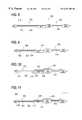
- FIG. 1shows a simplified circuit for a pixel of an exemplary CMOS imager using a photogate and having a pixel photodetector circuit 14 and a readout circuit 60 .
- FIG. 1shows the circuitry for operation of a single pixel, that in practical use there will be an M ⁇ N array of pixels arranged in rows and columns with the pixels of the array accessed using row and column select circuitry, as described in more detail below.
- the photodetector circuit 14is shown in part as a cross-sectional view of a semiconductor substrate 16 typically a p-type silicon, having a surface well of p-type material 20 .
- An optional layer 18 of p-type materialmay be used if desired, but is not required.
- Substrate 16may be formed of, for example, Si, SiGe, Ge, and GaAs.
- the entire substrate 16is p-type doped silicon substrate and may contain a surface p-well 20 (with layer 18 omitted), but many other options are possible, such as, for example p on p ⁇ substrates, p on p+ substrates, p-wells in n-type substrates or the like.
- wafer or substrate used in the descriptionincludes any semiconductor-based structure having an exposed surface in which to form the circuit structure used in the invention.
- Wafer and substrateare to be understood as including, silicon-on-insulator (SOI) technology, silicon-on-sapphire (SOS) technology, doped and undoped semiconductors, epitaxial layers of silicon supported by a base semiconductor foundation, and other semiconductor structures.
- SOIsilicon-on-insulator
- SOSsilicon-on-sapphire
- doped and undoped semiconductorssilicon-on-insulator
- epitaxial layers of silicon supported by a base semiconductor foundationand other semiconductor structures.
- previous process stepsmay have bee n utilized to form regions/junctions in the base semiconductor structure or foundation.
- An insulating layer 22such as, for example, silicon dioxide is formed on the upper surface of p-well 20 .
- the p-type layermay be a p-well formed in substrate 16 .
- a photogate 24thin enough to pass radiant energy or of a material which passes radiant energy is formed on the insulating layer 22 .
- the photogate 24receives an applied control signal PG which causes the initial accumulation of pixel charges in n+ region 26 .
- the n+ type region 26adjacent one side of photogate 24 , is formed in the upper surface of p-well 20 .
- a transfer gate 28is formed on insulating layer 22 between n+ type region 26 and a second n+ type region 30 formed in p-well 20 .
- the n+ regions 26 and 30 and transfer gate 28form a charge transfer transistor 29 which is controlled by a transfer signal TX.
- the n+ region 30is typically called a floating diffusion region. It is also a node for passing charge accumulated thereat to the gate of a source follower transistor 36 described below.
- a reset gate 32is also formed on insulating layer 22 adjacent and between n+ type region 30 and another n+ region 34 which is also formed in p-well 20 .
- the reset gate 32 and n+ regions 30 and 34form a reset transistor 31 which is controlled by a reset signal RST.
- the n+ type region 34is coupled to voltage source VDD.
- the transfer and reset transistors 29 , 31are n-channel transistors as described in this implementation of a CMOS imager circuit in a p-well. It should be understood that it is possible to implement a CMOS imager in an n-well in which case each of the transistors would be p-channel transistors. It should also be noted that while FIG. 1 shows the use of a transfer gate 28 and associated transistor 29 , this structure provides advantages, but is not required.
- Photodetector circuit 14also includes two additional n-channel transistors, source follower transistor 36 and row select transistor 38 .
- Transistors 36 , 38are coupled in series, source to drain, with the source of transistor 36 also coupled over lead 40 to voltage source VDD and the drain of transistor 38 coupled to a lead 42 .
- the drain of row select transistor 38is connected via conductor 42 to the drains of similar row select transistors for other pixels in a given pixel row.
- a load transistor 39is also coupled between the drain of transistor 38 and a voltage source VSS. Transistor 39 is kept on by a signal VLN applied to its gate.
- the imagerincludes a readout circuit 60 which includes a signal sample and hold (S/H) circuit including a S/H n-channel field effect transistor 62 and a signal storage capacitor 64 connected to the source follower transistor 36 through row transistor 38 .
- the other side of the capacitor 64is connected to a source voltage VSS.
- the upper side of the capacitor 64is also connected to the gate of a p-channel output transistor 66 .
- the drain of the output transistor 66is connected through a column select transistor 68 to a signal sample output node VOUTS and through a load transistor 70 to the voltage supply VDD.
- a signal called “signal sample and hold” (SHS)briefly turns on the S/H transistor 62 after the charge accumulated beneath the photogate electrode 24 has been transferred to the floating diffusion node 30 and from there to the source follower transistor 36 and through row select transistor 38 to line 42 , so that the capacitor 64 stores a voltage representing the amount of charge previously accumulated beneath the photogate electrode 24 .
- SHSsignal sample and hold
- the readout circuit 60also includes a reset sample and hold (S/H) circuit including a S/H transistor 72 and a signal storage capacitor 74 connected through the S/H transistor 72 and through the row select transistor 38 to the source of the source follower transistor 36 .
- the other side of the capacitor 74is connected to the source voltage VSS.
- the upper side of the capacitor 74is also connected to the gate of a p-channel output transistor 76 .
- the drain of the output transistor or 76is connected through a p-channel column select transistor 78 to a reset sample output node VOUTR and through a load transistor 80 to the supply voltage VDD.
- a signal called “reset sample and hold” (SHR)briefly turns on the S/H transistor 72 immediately after the reset signal RST has caused reset transistor 31 to turn on and reset the potential of the floating diffusion node 30 , so that the capacitor 74 stores the voltage to which the floating diffusion node 30 has been reset.
- the readout circuit 60provides correlated sampling of the potential of the floating diffusion node 30 , first of the reset charge applied to node 30 by reset transistor 31 and then of the stored charge from the photogate 24 .
- the two samplings of the diffusion node 30charges produce respective output voltages VOUTR and VOUTS, of the readout circuit 60 .
- These voltagesare then subtracted (VOUTS ⁇ VOUTR) by subtractor 82 to provide an output signal terminal 81 which is an image signal independent of pixel to pixel variations caused by fabrication variations in the reset voltage transistor 31 which might cause pixel to pixel variations in the output signal.
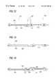
- FIG. 2illustrates a block diagram for a CMOS imager having a pixel array 200 with each pixel cell being constructed in the manner shown by element 14 of FIG. 1 .
- FIG. 4shows a 2 ⁇ 2 portion of pixel array 200 .
- Pixel array 200comprises a plurality of pixels arranged in a predetermined number of columns and rows. The pixels of each row in array 200 are all turned on at the same time by a row select line, e.g., line 86 , and the pixels of each column are selectively output by a column select line, e.g., line 42 .
- a plurality of rows and column linesare provided for the entire array 200 ,
- the row linesare selectively activated by the row driver 210 in response to row address decoder 220 and the column select lines are selectively activated by the column driver 260 in response to column address decoder 270 .
- a row and column addressis provided for each pixel.
- the CMOS imageris operated by the control circuit 250 which controls address decoders 220 , 270 for selecting the appropriate row and column lines for pixel readout, and row and column driver circuitry 210 , 260 which apply driving voltage to the drive transistors of the selected row and column lines.
- FIG. 3shows a simplified timing diagram for the signals used to transfer charge out of photodetector circuit 14 of the FIG. 1 CMOS imager.
- the photogate signal PGis nominally set to 5 V and the reset signal RST is nominally set at 2.5 V.
- the processis begun at time t 0 by briefly pulsing reset voltage RST to 5 V.
- the RST voltagewhich is applied to the gate 32 of reset transistor 31 , causes transistor 31 to turn on and the floating diffusion node 30 to charge to the VDD voltage present at n+ region 34 (less the voltage drop Vth of transistor 31 ). This resets the floating diffusion node 30 to a predetermined voltage (VDD-Vth).
- the charge on floating diffusion node 30is applied to the gate of the source follower transistor 36 to control the current passing through transistor 38 , which has been turned on by a row select (ROW) signal, and load transistor 39 .
- This currentis translated into a voltage on line 42 which is next sampled by providing a SHR signal to the S/H transistor 72 which charges capacitor 74 with the source follower transistor output voltage on line 42 representing the reset charge present at floating diffusion node 30 .
- the PG signalis next pulsed to 0 volts, causing charge to be collected in n+ region 26 .
- a transfer gate voltage pulse TXsimilar to the reset pulse RST, is then applied to transfer gate 28 of transistor 29 to cause the charge in n+ region 26 to transfer to floating diffusion node 30 .
- the transfer gate voltage TXmay be pulsed or held to a fixed DC potential.
- the transfer gate voltage TXmust be pulsed.
- the new output voltage on line 42 generated by source follower transistor 36 currentis then sampled onto capacitor 64 by enabling the sample and hold switch 62 by signal SHS.
- the column select signalis next applied to transistors 68 and 70 and the respective charges stored in capacitors 64 and 74 are subtracted in subtractor 82 to provide a pixel output signal at terminal 81 .
- CMOS imagersmay dispense with the transistor gate 28 and associated transistor 26 or retain these structures while biasing the transfer transistor gate 28 to an always “on” state.
- CMOS imagerThe operation of the charge collection of the CMOS imager is known in the art and is described in several publications such as Mendis et al., “Progress in CMOS Active Pixel Image Sensors,” SPIE Vol. 2172, pp. 19-29 1994; Mendis et al., “CMOS Active Pixel Image Sensors for Highly Integrated Imaging Systems,” IEEE Journal of Solid State Circuits, Vol. 32(2), 1997; and Eric R, Fossum, “CMOS Image Sensors: Electronic Camera on a Chip,” IEDM Vol. 95 pages 17-25 (1995) as well as other publications. These references are incorporated herein by reference.
- CMOS imagerssuffer from several drawbacks regarding the charge flow and contact between the floating diffusion area 30 and the source follower transistor 36 .
- cautionmust be taken to avoid over etching into the shallow n-doped region of the floating diffusion region so as to prevent potential charge leakage into the substrate during operation of the imager.
- the signal to noise ratio of the pixelshould be as high as possible within a pixel. Thus, leakage into the substrate is a significant problem to be avoided in CMOS imagers.
- the tungsten metalwhich is typically used to contact the floating diffusion region and the source follower transistor, is deposited with tungsten fluoride and a reaction sometimes takes place between the tungsten fluoride and the substrate resulting in the formation of silicon fluoride which creates worm holes in the substrate. These worm holes create a conductive channel for current to leak into the substrate, creating a poor performance for the imager.
- conventional floating diffusion regionstypically have a highly n-doped region to facilitate an ohmic metal-semiconductor contact between the contact metallization and the underlying n-doped silicon region to achieve charge transfer to the source follower transistor 36 .
- this same highly doped n+ region 30creates current leakage into the substrate due to high electric fields caused by the abrupt junction. Also, typically there must be an over etch of the contact to account for non-uniformities across the wafer and non-uniformity of the BPSG thickness Accordingly, resistance in the conductive path between the floating diffusion fusion region and gate of the source follower transistor should be as low as possible without resulting in added junction leakage.
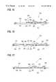
- FIGS. 5-7show a side view of several CMOS imagers of the prior art. It should be understood that similar reference numbers correspond to similar elements for FIGS. 5-7.
- FIG. 5This figure shows the region between the floating diffusion and the source follower transistor of a prior CMOS imager having a photogate as the photoactive area and further includes a transfer gate.
- the imager 100is provided with three doped regions 143 , 126 and 115 , which are doped to a conductivity type different from that of the substrate, for exemplary purposes regions 143 , 126 and 115 are treated as n type, which are within a p-well of a substrate.
- the first doped region 143is the photosite charge collector, and it underlies a portion of the photogate 142 , which is a thin layer of material transparent or partially transparent to radiant energy, such as polysilicon.
- the first doped region 143is typically an n-doped region.
- An insulating layer 140 of silicon dioxide, silicon nitride, or other suitable materialis formed over a surface of the doped layer 143 of the substrate between the photogate 142 and first doped region 143 .
- the second doped region 126transfers charge collected by the photogate 142 and it serves as the source for the transfer transistor 128 .
- the transfer transistor 128includes a transfer gate 139 formed over a gate oxide layer 140 .
- the transfer gate 139has insulating spacers 149 formed on its sides.
- the third doped region 115is the floating diffusion region and is connected to a gate 136 of a source follower transistor by contact lines 125 , 127 , 129 which are typically metal contact lines as described in more detail below.
- the imager 100typically includes a highly n+ doped region 120 within n-doped region 115 under the floating diffusion region contact 125 which provides good ohmic contact of the contact 125 with the n-doped region 115 .
- the floating diffusion contact 125connects n+ region 120 of the floating diffusion region with the gate 136 of the source follower transistor.
- the entire region 115may be doped n+ thereby eliminating the need for n+ region 120 .
- the source and drain regions of the source follower transistorare not seen in FIG. 5 as they are perpendicular to the page but are on either side of gate 136 .
- the source follower gate 136is usually formed of a doped polysilicon which may be silicided and which is deposited over a gate oxide 140 , such as silicon dioxide.
- the floating diffusion contact 125is usually formed of a tungsten plug typically a Ti/TiN/W metallization stack as described in further detail below.
- the floating diffusion contact 125is formed in an insulating layer 135 which is typically an undoped oxide followed by the deposition of a doped oxide such as a BPSG layer deposited over the substrate.
- the tungsten metal which forms the floating diffusion/source follower contact 125is typically deposited using a tungsten fluoride such as WF 6 .
- the layer 135must be etched with a selective dry etch process prior to depositing the tungsten plug connector 125 .
- the imager 100also include a source follower contact 127 formed in layer 135 in a similar fashion to floating diffusion contact 125 .
- Source follower contact 127is also usually formed of a tungsten plug typically a Ti/TiN/W metallization stack as described in further detail below.
- the floating diffusion contact 125 and the source follower contact 127are connected by a metal layer 129 formed over layer 135 .
- metal layer 129is formed of aluminum, copper or any other metal.
- the field oxide 132may be formed by thermal oxidation of the substrate or in the Local Oxidation of Silicon (LOCOS) or by the Shallow Trench Isolation (STI) process which involves the chemical vapor deposition of an oxide material.
- LOCOSLocal Oxidation of Silicon
- STIShallow Trench Isolation
- FIG. 5shows an imager having a photogate as the photoactive area and additionally includes a transfer transistor
- additional imager structuresare also well known.
- CMOS imagers having a photodiode or a photoconductor as the photoactive areaare known.
- a transfer transistorhas some advantages as described above, it is not required.
- the prior art metal contacts 125 , 127 described with reference to FIG. 5typically include a thin layer 123 formed of titanium, titanium nitride or a mixture thereof formed in the etched space in the layer 135 .
- a tungsten plug 122is then filled in the etched space in the layer 135 inside the thin layer 123 .
- the contact 125contacts n+ region 120 and forms a TiSi 2 area 121 by a reaction between the titanium from layer 123 with the silicon substrate in n+ region 120 .
- FIG. 6This figure illustrates a partially cut away side view of a semiconductor imager undergoing a processing method according to the prior art.
- the imager 104has the floating diffusion region 115 having an n+ doped region 120 and the source follower transistor gate 136 already formed therein.
- the floating diffusion 115 and the source follower gate 136are under layer 135 , which, as noted, is preferably composed of oxides, typically a layered structure of an undoped and doped, i.e., BPSG, oxides.
- a resist 155is applied to layer 135 in order to etch through layer 135 to form the contacts to the floating diffusion region 115 and the source follower transistor gate 136 .
- Layer 135is then etched to form the hole 156 in layer 135 for the floating diffusion contact 125 and hole 157 in layer 135 for the source follower transistor contact 127 as shown in FIG. 7 .
- the field oxide 132 and layer 135are both similar oxides it is difficult to control the etching process when attempting to align the hole 156 with the edge of the field oxide 132 .
- the etching processoften etches deep into the n+ region 120 or etches through the exposed edge of the field oxide 132 causing charge leakage to the substrate as shown by the arrows in FIG. 7 .
- Etching deep into the n+ region 120results in poor contact resistance to the n+ region 120 .
- Etching through the n+ region 120 or through the exposed region of the filed oxide 132can result in charge leakage to the substrate.
- the devices described with reference to FIGS. 5-7have several drawbacks. For example, during etching, caution must be taken to avoid etching through the n+ layer 120 or even deep into n-doped region 115 where the n-type dopant concentration is reduced. Additionally, when the tungsten metal is deposited by the tungsten fluoride, a reaction sometimes takes place between the tungsten fluoride and the substrate resulting in the formation of silicon fluoride which creates worm holes through the n+ region 120 and into the substrate. These worm holes may create a channel for current to leak into the substrate, creating a poor performance for the imager.
- the prior art floating diffusion region 115included the highly n+ region 120 to provide an ohmic contact; however, this same highly doped n+ region sets up high electric fields with respect to the p-type region under field oxide region 132 which fosters current leakage into the substrate. Accordingly, a better low resistance conductive path is required between region 120 and gate 136 of the source follower transistor which provides a good ohmic contact, while avoiding substrate leakage.
- the present inventionprovides a CMOS imager in which the floating diffusion is connected to a gate of the source follower transistor through a buried contact.
- the buried contact between the floating diffusion and the gate of the source follower transistoris formed on the substrate and under the BPSG layer to reduce the, need to etch holes in the BPSG layer.
- the buried contactprovides a better ohmic contact with less leakage into the substrate.
- the buried contact between the floating diffusion region and the gate of the source follower transistoralso allows the floating diffusion region and the source follower transistor to be placed closer together, thereby reducing size of a pixel and allowing an increased photoarea per cell size which, it turn, increases the signal to noise ratio of the imager.
- the problems with worm holes and connecting of the floating diffusion contactare completely avoided as there is no need for the highly doped n+ region 120 in the present invention and additionally no need for any metallization to be directly in contact with the silicon substrate at the floating diffusion node.
- FIG. 1is a representative circuit of a CMOS imager.
- FIG. 2is a block diagram of a CMOS active pixel sensor chip.
- FIG. 3is a representative timing diagram for the CMOS imager.
- FIG. 4is a representative pixel layout showing a 2 ⁇ 2 pixel layout according to one embodiment of the present invention.
- FIG. 5is a partially cut away side view of a semiconductor imager having a photogate and a transfer gate according to the prior art.
- FIG. 6shows a partially cut away side view of a semiconductor imager undergoing a processing method according to the prior art.
- FIG. 7shows a partially cut away side view of a semiconductor imager undergoing a processing method according to the prior art subsequent to FIG. 6 .
- FIG. 8shows a partially cut away side view of a semiconductor imager of a first embodiment of the present invention at an intermediate step of processing.
- FIG. 9shows a partially cut away side view of a semiconductor imager of the present invention subsequent to FIG. 8 .
- FIG. 10shows a partially cut away side view of a semiconductor imager of the present invention subsequent to FIG. 9 .
- FIG. 11shows a partially cut away side view of a semiconductor imager of the present invention subsequent to FIG. 10 .
- FIG. 12shows a partially cut away side view of a semiconductor imager undergoing a processing method according to a second embodiment the present invention.
- FIG. 13shows a partially cut away side view of a semiconductor imager undergoing a processing method according to a second embodiment the present invention subsequent to FIG. 12 .
- FIG. 14shows a partially cut away side view of a semiconductor imager undergoing a processing method according to a second embodiment the present invention subsequent to FIG. 13 .
- FIG. 15shows a partially cut away side view of a semiconductor imager of a third embodiment of the present invention at an intermediate step of processing.
- FIG. 16shows a partially cut away side view of a semiconductor imager of a fourth embodiment of the present invention at an intermediate step of processing.
- FIG. 17shows a partially cut away side view of a semiconductor imager of a fifth embodiment of the present invention at an intermediate step of processing.
- FIG. 18is an illustration of a computer system having a CMOS imager according to the present invention.
- wafer and substrateare to be understood as including silicon-on-insulator (SOI) or silicon-on-sapphire (SOS) technology, doped and undoped semiconductors, epitaxial layers of silicon supported by a base semiconductor foundation, and other semiconductor structures.
- SOIsilicon-on-insulator
- SOSsilicon-on-sapphire
- doped and undoped semiconductorsepitaxial layers of silicon supported by a base semiconductor foundation
- previous process stepsmay have been utilized to form regions or junctions in the base semiconductor structure or foundation.
- the semiconductorneed not be silicon-based, but could be based on silicon-germanium, germanium, or gallium arsenide.
- pixelrefers to a picture element unit cell containing a photosensor and transistors for converting electromagnetic radiation to an electrical signal.
- a representative pixelis illustrated in the figures and description herein, and typically fabrication of all pixels in an imager will proceed simultaneously in a similar fashion.
- the following detailed descriptionis, therefore, not to be taken in a limiting sense, and the scope of the present invention is defined by the appended claims.
- FIG. 8shows a partially cut away cross-sectional view of a CMOS semiconductor wafer similar to that shown in FIG. 1 . It should be understood that similar reference numbers correspond to similar elements for FIGS. 8-17.
- FIG. 8shows the region between the floating diffusion and the source follower transistor for an imager having a photodiode as the photosensitive area and which does not include a transfer gate. As with FIG. 5 above, the source follower transistor source and drain regions are in a plane perpendicular to FIG. 8 .
- the pixel cell 300includes a substrate which includes a p-type well 311 formed in a substrate.
- the pixel cell 300includes an n-doped region 315 which forms the floating diffusion region. It should be understood that the CMOS imager of the present invention can also be fabricated using p-doped regions in an n-well.
- the pixel cell 300also includes a field oxide region 332 , which serves to surround and isolate the cells which may be formed by thermal oxidation of the substrate using the LOCOS process or by the STI process which involve the chemical vapor deposition of an oxide material.
- the field oxide region 332form an isolation around the source follower transistor area 330 .
- the pixel cell 300includes an oxide or other insulating film 318 deposited on the substrate by conventional methods.
- the oxide film 318is formed of a silicon dioxide grown onto the substrate.
- An n-doped region 315is shown in FIG. 8 .
- Doped region 352is formed in the substrate as shown in FIG. 8 in the area that will later become the photodiode 350 .
- the regions 315 and 352may be doped to the same or different conductivity types and also to differing dopant concentration levels. Additionally, while two separate doped regions are shown in the figure, a single doped region may incorporate both regions 315 and 352 .
- There may be other dopant implantation applied to the wafer at this stage of processingsuch as n-well and p-well implants or transistor voltage adjusting implants. For simplicity, these other implants are not shown in the figure.
- patterned resist(not shown ) is applied to the substrate.
- the oxide film 318is etched through the exposed regions of the resist where the buried contacts are desired to be formed, such as over the floating diffusion region 315 , as shown in FIG. 9 .
- the etchingmay be achieved by any conventional methods such as a wet etch or a dry etch.
- a doped polysilicon layer 320is next deposited over the pixel cell 300 and patterned using resist and etching methods.
- the doped polysilicon layer 320is deposited according to conventional methods.
- the doped polysilicon layer 320will form the buried conductor between the floating diffusion region 315 and will also act as the gate for the source follower transistor.
- the n-type dopant from in the doped polysilicon layer 320diffuses out of the doped polysilicon and into n-doped region 315 to form buried contact region 325 . Buried contact 325 forms a good low leakage damage free contact to n-doped region 315 .
- the doped polysilicon layer 320additionally serves as the transistor gate for the source follower transistor.
- FIG. 10shows the doped polysilicon layer 320 after it has been etched by conventional methods to form a contact from the floating diffusion region 315 to the source follower transistor.
- the doped polysilicon layer 320may be formed of a composite layered structure of doped polysilicon/refractory metal silicide or doped polysilicon/refractory method silicide/insulator for improved conductivity, if desired, according to conventional methods.
- the refractory metal silicideis a tungsten, cobalt silicide or titanium silicide.
- the pixel cell 300 of the present inventionis then processed according to known methods to produce an operative imaging device.
- the buried contact 325is considered buried because of additional material layers which are fanned over the substrate to produce an operative CMOS imager circuit.
- an insulating layer 360may be applied and planarized and contact holes etched therein as shown in FIG. 11 to form conductor paths to transistor gates, etc.
- the layer 360may include materials such as BPSG, PSG, BSG or the like.
- Conventional metal and insulation layersare formed over layer 360 and in the through holes to interconnect various parts of the circuitry in a manner similar to that used in the prior art to form the floating diffusion region to source follower gate connection.
- the imageris fabricated to arrive at an operational apparatus that functions similar to the imager depicted in FIGS. 1-4.
- the buried contact 325is well below the normal metal layers which are applied over layer 360 and which are used to interconnect the IC circuitry to produce a CMOS imager.
- the buried contact 325 between the floating diffusion region 315 and the conductive polysilicon layer 320provides a good contact between the floating diffusion region and the source follower transistor without using processing techniques which might cause charge leakage to the substrate during device operation.
- the buried contact 325 and the doped polysilicon layer 320also allow the source follower transistor to be placed closer to the floating diffusion region thereby allowing an increased photosensitive area on the pixel and short conductor between the floating diffusion region and gate of the source follower transistor which increases the signal to noise ratio of the imager.
- FIG. 12illustrates a partially cut away side view of a semiconductor imager undergoing a processing method according to a second embodiment of the present invention.
- a resist layer 355is applied to the pixel cell as shown in the figure.
- a contact space 357is provided in the resist. As shown in the figure, the contact space 357 is aligned over n-doped region 315 and may overlap field oxide region 332 . Since there is no heavily doped n+ region in the imager of the present invention, it is not critic that doped polysilicon layer 320 be directly aligned over a specific portion of the floating diffusion region as in the prior art.
- the insulating layer 318 and the field oxide 332are then etched as shown in FIG. 13 .
- the doped polysilicon layer 320is next deposited over the pixel cell 300 and the oxide film 318 . As set forth above, the doped polysilicon layer 320 is deposited according to conventional methods. The doped polysilicon layer 320 forms the buried contact 325 between the floating diffusion region 315 and the source follower transistor. Either during the growth of the doped polysilicon layer 320 , or in subsequent thermal steps, dopant diffuses out of the doped polysilicon layer 320 and into n-doped region 315 to form buried contact region 325 . Buried contact 325 forms a good low leakage damage free contact to n-doped region 315 . The doped polysilicon layer 320 may additionally serves as the transistor gate for the source follower transistor. The doped polysilicon layer 320 is then etched by conventional methods to form a contact from the floating diffusion region 315 to the source follower transistor as shown in FIG. 14 .
- the doped polysilicon layer 320may be formed of a composite layered structure of doped polysilicon/refractory metal silicide or doped polysilicon/refractory metal silicide/insulator for improved conductivity, if desired, according to conventional methods.
- the method according to the second embodiment of the inventionallows the source follower transistor and the floating diffusion region to be placed closer together to allow for a larger active area within the pixel cell.
- the second embodiment of the present inventionadditionally allows for a smaller overlap of the doped polysilicon layer 320 into the doped region diffusion region 315 thus making a larger photosensitive area possible while still being able to adequately contact the source follower transistor gate to the floating diffusion region 315 due to buried contact 325 .
- FIG. 15illustrates a partially cut away side view of a CMOS pixel cell 301 of a third embodiment of the present invention at an intermediate step of processing.
- This figureshows the region between the floating diffusion and the source follower transistor of a CMOS imager having a photodiode as the photoactive area and further includes a transfer transistor 328 .
- the pixel cell 301is provided with two n-doped regions 352 and 315 , which are doped to a conductivity type different from that of the substrate well, which for exemplary purposes is treated as a p-type well 311 .
- the first doped region 352is the photosite charge collector.
- the second doped region 315is the floating diffusion region and is connected to source follower transistor by buried contact 325 via doped polysilicon layer 320 which may also function as the gate for the source follower transistor.
- the transfer transistor 328includes a transfer gate 339 formed over a gate oxide layer 318 as is understood to be conventional in the art.
- the transfer transistor 328 and the source follower transistorhave insulating spacers 349 formed on sides of the transistor gates.
- FIG. 16illustrates a CMOS imager pixel cell 302 according to a fourth embodiment of the present invention.
- the pixel cell 302includes a photogate as the photoactive area and further includes a transfer transistor 328 .
- the pixel cell 302is provided with three doped regions 343 , 326 and 315 , which are doped to a conductivity type different from that of the substrate.
- regions 343 , 346 and 315are doped as n type with the substrate having a p-type well 311 .
- the first doped region 343is the photosite charge collector, and it underlies a portion of the photogate 342 , which is a thin layer of material transparent or semi-transparent to radiant energy, such as but not limited to polysilicon.
- the first doped region 343is typically doped n ⁇ .
- An insulating layer 318 of silicon dioxide, silicon nitride, or other suitable materialis formed over a surface of the doped layer 343 of the substrate between the photogate 342 and first doped region 343 .
- the second doped region 326transfers charge collected by the photogate 342 and it serves as the source for the transfer transistor 328 .
- the transfer transistor 328includes a doped polysilicon layer 339 formed over a gate oxide layer 318 18 as is understood to be conventional to the person having ordinary skill in the art.
- the transfer transistor 328has spacers 349 formed around its gate 339 .
- the third doped region 315is the floating diffusion region and is connected to source follower transistor by buried contact 325 via doped polysilicon layer 320 which may also function as the gate for the source follower transistor.
- FIG. 17illustrates a fifth embodiment of the present invention at an intermediate step of processing.
- the pixel cell 303includes a photogate as the photoactive area and omits a transfer transistor.
- the pixel cell 303is provided with two doped regions 343 and 315 , which are doped to a conductivity type different from that of the substrate.
- regions 343 and 315is treated as doped n-type for use in a p-type well 311 in the substrate.
- the first doped region 343is the photosite charge collector, and it underlies a portion of the photogate 342 .
- An insulating layer 318is formed over a surface of the doped layer 343 of the substrate between the photogate 342 and first doped region 343 .
- the second doped region 315is the floating diffusion region and is connected to source follower transistor by buried contact 325 and doped polysilicon layer 320 which may also function as the gate for the source follower transistor.
- CMOS imagersrepresentative of those discussed above with reference to FIGS. 1-4 and having the buried conductor of the present invention.
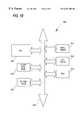
- a typical processor based system which includes a CMOS imager device according to the present inventionis illustrated generally at 500 in FIG. 18.
- a processor based systemis exemplary of a system having, digital circuits which could include CMOS imager devices. Without being limiting, such a system could include a computer system, camera system, scanner, machine vision vehicle navigation, video phone, surveillance system, auto focus system, star tracker system, motion detection system, image stabilization system and data compression system for high-definition television, all of which can utilize the present invention.
- a processor based systemsuch as a computer system, for example generally comprises a central processing unit (CPU) 544 , for example, a microprocessor, that communicates with an input/output (I/O) device 546 over a bus 552 .
- the CMOS imager 542also communicates with the system over bus 452 .
- the computer system 500also includes random access memory (RAM) 548 , and, in the case of a computer system may include peripheral devices such as a floppy disk drive 554 and a compact disk (CD) ROM drive 556 which also communicate with CPU 544 over the bus 552 .
- RAMrandom access memory
- CMOS imager 542is preferably constructed as an integrated circuit which includes the CMOS imager having a buried contact line between the floating diffusion region and the source follower transistor, as previously described with respect to FIGS. 8-18. It may also be desirable to integrate the processor 554 , CMOS imager 542 and memory 548 on a single IC chip.
- CMOS imaging circuits having a photogate and a floating diffusionthe invention has broader applicability and may be used in any CMOS imaging apparatus.
- the CMOS imager arraycan be formed on a single chip together with the logic or the logic and array may be formed on separate IC chips.
- any type of photocollection devicessuch as photogates, photoconductors or the like may find use in the present invention.
- the process described aboveis but one method of many that could be used.
Landscapes
- Solid State Image Pick-Up Elements (AREA)
Abstract
Description
Claims (27)
Priority Applications (1)
| Application Number | Priority Date | Filing Date | Title |
|---|---|---|---|
| US09/457,264US6291280B1 (en) | 1998-11-12 | 1999-12-09 | CMOS imager cell having a buried contact and method of fabrication |
Applications Claiming Priority (2)
| Application Number | Priority Date | Filing Date | Title |
|---|---|---|---|
| US09/190,055US6740915B1 (en) | 1998-11-12 | 1998-11-12 | CMOS imager cell having a buried contact |
| US09/457,264US6291280B1 (en) | 1998-11-12 | 1999-12-09 | CMOS imager cell having a buried contact and method of fabrication |
Related Parent Applications (1)
| Application Number | Title | Priority Date | Filing Date |
|---|---|---|---|
| US09/190,055DivisionUS6740915B1 (en) | 1998-11-12 | 1998-11-12 | CMOS imager cell having a buried contact |
Publications (1)
| Publication Number | Publication Date |
|---|---|
| US6291280B1true US6291280B1 (en) | 2001-09-18 |
Family
ID=22699848
Family Applications (2)
| Application Number | Title | Priority Date | Filing Date |
|---|---|---|---|
| US09/190,055Expired - LifetimeUS6740915B1 (en) | 1998-11-12 | 1998-11-12 | CMOS imager cell having a buried contact |
| US09/457,264Expired - LifetimeUS6291280B1 (en) | 1998-11-12 | 1999-12-09 | CMOS imager cell having a buried contact and method of fabrication |
Family Applications Before (1)
| Application Number | Title | Priority Date | Filing Date |
|---|---|---|---|
| US09/190,055Expired - LifetimeUS6740915B1 (en) | 1998-11-12 | 1998-11-12 | CMOS imager cell having a buried contact |
Country Status (1)
| Country | Link |
|---|---|
| US (2) | US6740915B1 (en) |
Cited By (24)
| Publication number | Priority date | Publication date | Assignee | Title |
|---|---|---|---|---|
| US6410951B2 (en)* | 2000-03-21 | 2002-06-25 | Micron Technology, Inc. | Structure for improving static refresh |
| US6472245B2 (en)* | 2000-08-31 | 2002-10-29 | Hyundai Electronics Industries Co., Ltd. | Image sensor forming method capable of defining connection window structure by etching field oxide |
| EP1309007A2 (en) | 2001-11-06 | 2003-05-07 | Omnivision Technologies Inc. | Active pixel having reduced dark current in a cmos image sensor |
| US6607951B2 (en)* | 2001-06-26 | 2003-08-19 | United Microelectronics Corp. | Method for fabricating a CMOS image sensor |
| US20040041227A1 (en)* | 2002-08-28 | 2004-03-04 | Ward Joseph A. | Intermeshed guard bands for multiple voltage supply structures on an integrated circuit, and methods of making same |
| US20040053436A1 (en)* | 1999-08-16 | 2004-03-18 | Rhodes Howard E. | Buried channel CMOS imager and method of forming same |
| US20040089883A1 (en)* | 2002-08-20 | 2004-05-13 | Kim Yi-Tae | CMOS image sensor and method of fabricating the same |
| US20040173864A1 (en)* | 2003-03-07 | 2004-09-09 | Makoto Inagaki | Solid-state imaging device |
| US20040188728A1 (en)* | 2003-02-21 | 2004-09-30 | Stmicroelectronics Ltd. | CMOS image sensors |
| US20040245596A1 (en)* | 2003-06-06 | 2004-12-09 | Renesas Technology Corp. | Semiconductor device having trench isolation |
| US20050023580A1 (en)* | 2003-04-25 | 2005-02-03 | Howard Rhodes | Imager floating diffusion region and process for forming same |
| US6879340B1 (en) | 1998-08-19 | 2005-04-12 | Micron Technology Inc. | CMOS imager with integrated non-volatile memory |
| US20050087782A1 (en)* | 2003-10-22 | 2005-04-28 | Rhodes Howard E. | Optimized photodiode process for improved transfer gate leakage |
| US20050093088A1 (en)* | 2003-10-29 | 2005-05-05 | Kyung-Lak Lee | Isolation layer for CMOS image sensor and fabrication method thereof |
| US20050161713A1 (en)* | 2003-04-25 | 2005-07-28 | Howard Rhodes | Imager floating diffusion region and process for forming same |
| US20050167711A1 (en)* | 2003-06-16 | 2005-08-04 | Chandara Mouli | Photodiode with ultra-shallow junction for high quantum efficiency CMOS image sensor and method of formation |
| EP1566842A2 (en)* | 2004-02-19 | 2005-08-24 | Canon Kabushiki Kaisha | Solid-state image pick-up device and image system using the same |
| US20050184321A1 (en)* | 2004-02-25 | 2005-08-25 | National Semiconductor Corporation | Low dark current CMOS image sensor pixel having a photodiode isolated from field oxide |
| US20060043436A1 (en)* | 2004-09-02 | 2006-03-02 | Micron Technology, Inc. | Contacts for CMOS imagers and method of formation |
| US20060273354A1 (en)* | 2005-06-03 | 2006-12-07 | Magnachip Semiconductor, Ltd. | Pixel of image sensor and method for fabricating the same |
| US20070017832A1 (en)* | 2005-06-24 | 2007-01-25 | J-Lok Co. | Device for forming partitioned film packages |
| US20170200759A1 (en)* | 2016-01-12 | 2017-07-13 | Samsung Electronics Co Ltd | CMOS Image Sensors |
| US20190109169A1 (en)* | 2017-10-10 | 2019-04-11 | Omnivision Technologies, Inc. | Source follower contact |
| CN113013186A (en)* | 2019-12-20 | 2021-06-22 | 豪威科技股份有限公司 | Tunnel contact for pixel cell in imaging system |
Families Citing this family (8)
| Publication number | Priority date | Publication date | Assignee | Title |
|---|---|---|---|---|
| US20040164331A1 (en)* | 2002-06-11 | 2004-08-26 | Chih-Wei Hung | CMOS image sensor device and process of producing the same |
| KR100508086B1 (en)* | 2002-09-11 | 2005-08-17 | 삼성전자주식회사 | Cmos image sensor and method of fabricating the same |
| JP2004304012A (en)* | 2003-03-31 | 2004-10-28 | Matsushita Electric Ind Co Ltd | Solid-state imaging device and method of manufacturing the same |
| US7345330B2 (en)* | 2004-12-09 | 2008-03-18 | Omnivision Technologies, Inc. | Local interconnect structure and method for a CMOS image sensor |
| US7115924B1 (en)* | 2005-06-03 | 2006-10-03 | Avago Technologies Sensor Ip Pte. Ltd. | Pixel with asymmetric transfer gate channel doping |
| US7514716B2 (en)* | 2006-08-29 | 2009-04-07 | Aptina Imaging Corporation | In-pixel analog memory with non-destructive read sense circuit for high dynamic range global shutter pixel operation |
| KR20080023774A (en)* | 2006-09-12 | 2008-03-17 | 동부일렉트로닉스 주식회사 | Photodiode of CMOS image sensor |
| US10957186B2 (en)* | 2018-11-29 | 2021-03-23 | Omnivision Technologies, Inc. | Reducing false alarms in surveillance systems |
Citations (13)
| Publication number | Priority date | Publication date | Assignee | Title |
|---|---|---|---|---|
| US4374700A (en) | 1981-05-29 | 1983-02-22 | Texas Instruments Incorporated | Method of manufacturing silicide contacts for CMOS devices |
| US5319604A (en) | 1990-05-08 | 1994-06-07 | Texas Instruments Incorporated | Circuitry and method for selectively switching negative voltages in CMOS integrated circuits |
| US5461425A (en) | 1994-02-15 | 1995-10-24 | Stanford University | CMOS image sensor with pixel level A/D conversion |
| US5471515A (en) | 1994-01-28 | 1995-11-28 | California Institute Of Technology | Active pixel sensor with intra-pixel charge transfer |
| US5541402A (en) | 1994-10-17 | 1996-07-30 | At&T Corp. | Imaging active pixel device having a non-destructive read-out gate |
| US5576763A (en) | 1994-11-22 | 1996-11-19 | Lucent Technologies Inc. | Single-polysilicon CMOS active pixel |
| US5612799A (en) | 1990-11-26 | 1997-03-18 | Semiconductor Energy Laboratory Co., Inc. | Active matrix type electro-optical device |
| US5614744A (en) | 1995-08-04 | 1997-03-25 | National Semiconductor Corporation | CMOS-based, low leakage active pixel array with anti-blooming isolation |
| US5625210A (en) | 1995-04-13 | 1997-04-29 | Eastman Kodak Company | Active pixel sensor integrated with a pinned photodiode |
| US5705846A (en) | 1995-07-31 | 1998-01-06 | National Semiconductor Corporation | CMOS-compatible active pixel image array using vertical pnp cell |
| US5708263A (en) | 1995-12-27 | 1998-01-13 | International Business Machines Corporation | Photodetector array |
| US5757045A (en) | 1996-07-17 | 1998-05-26 | Taiwan Semiconductor Manufacturing Company Ltd. | CMOS device structure with reduced risk of salicide bridging and reduced resistance via use of a ultra shallow, junction extension, ion implantation |
| US6040593A (en)* | 1998-06-29 | 2000-03-21 | Hyundai Electronics Industries Co., Ltd. | Image sensor having self-aligned silicide layer |
Family Cites Families (3)
| Publication number | Priority date | Publication date | Assignee | Title |
|---|---|---|---|---|
| US4309624A (en)* | 1979-07-03 | 1982-01-05 | Texas Instruments Incorporated | Floating gate amplifier method of operation for noise minimization in charge coupled devices |
| JPS5738073A (en)* | 1980-08-20 | 1982-03-02 | Hitachi Ltd | Solid-state image sensor |
| US5789774A (en)* | 1996-03-01 | 1998-08-04 | Foveonics, Inc. | Active pixel sensor cell that minimizes leakage current |
- 1998
- 1998-11-12USUS09/190,055patent/US6740915B1/ennot_activeExpired - Lifetime
- 1999
- 1999-12-09USUS09/457,264patent/US6291280B1/ennot_activeExpired - Lifetime
Patent Citations (13)
| Publication number | Priority date | Publication date | Assignee | Title |
|---|---|---|---|---|
| US4374700A (en) | 1981-05-29 | 1983-02-22 | Texas Instruments Incorporated | Method of manufacturing silicide contacts for CMOS devices |
| US5319604A (en) | 1990-05-08 | 1994-06-07 | Texas Instruments Incorporated | Circuitry and method for selectively switching negative voltages in CMOS integrated circuits |
| US5612799A (en) | 1990-11-26 | 1997-03-18 | Semiconductor Energy Laboratory Co., Inc. | Active matrix type electro-optical device |
| US5471515A (en) | 1994-01-28 | 1995-11-28 | California Institute Of Technology | Active pixel sensor with intra-pixel charge transfer |
| US5461425A (en) | 1994-02-15 | 1995-10-24 | Stanford University | CMOS image sensor with pixel level A/D conversion |
| US5541402A (en) | 1994-10-17 | 1996-07-30 | At&T Corp. | Imaging active pixel device having a non-destructive read-out gate |
| US5576763A (en) | 1994-11-22 | 1996-11-19 | Lucent Technologies Inc. | Single-polysilicon CMOS active pixel |
| US5625210A (en) | 1995-04-13 | 1997-04-29 | Eastman Kodak Company | Active pixel sensor integrated with a pinned photodiode |
| US5705846A (en) | 1995-07-31 | 1998-01-06 | National Semiconductor Corporation | CMOS-compatible active pixel image array using vertical pnp cell |
| US5614744A (en) | 1995-08-04 | 1997-03-25 | National Semiconductor Corporation | CMOS-based, low leakage active pixel array with anti-blooming isolation |
| US5708263A (en) | 1995-12-27 | 1998-01-13 | International Business Machines Corporation | Photodetector array |
| US5757045A (en) | 1996-07-17 | 1998-05-26 | Taiwan Semiconductor Manufacturing Company Ltd. | CMOS device structure with reduced risk of salicide bridging and reduced resistance via use of a ultra shallow, junction extension, ion implantation |
| US6040593A (en)* | 1998-06-29 | 2000-03-21 | Hyundai Electronics Industries Co., Ltd. | Image sensor having self-aligned silicide layer |
Non-Patent Citations (29)
| Title |
|---|
| Dickinson, A., et al., A 256×256 CMOS Active Pixel Image Sensor with Motion Detection, 1995 IEEE International Solid-State Circuits Conference, pp. 226-227. |
| Dickinson, A., et al., A 256x256 CMOS Active Pixel Image Sensor with Motion Detection, 1995 IEEE International Solid-State Circuits Conference, pp. 226-227. |
| Dickinson, A., et al., Standard CMOS Active Pixel Image Sensors for Multimedia Applications, Proceedings of Sixteenth Conference on Advanced Research in VLSI, Mar. 27-29, 1995, pp. 214-224. |
| Eid, E-S., et al., A 256×256 CMOS Active Pixel Image Sensor, Proc. SPIE vol. 2415, Apr. 1995, pp. 265-275. |
| Eid, E-S., et al., A 256x256 CMOS Active Pixel Image Sensor, Proc. SPIE vol. 2415, Apr. 1995, pp. 265-275. |
| Fossum, E., Architectures for focal plane image processing, Optical Engineering, vol. 28, No. 8, Aug. 1989, pp. 865-871. |
| Fossum, E., CMOS Image Sensors: Electronic Camera On A Chip, 1995 IEEE, pp. 17-25. |
| Fossum, E., et al., IEDM A 37×28mm2 600k-Pixel CMOS APS Dental X-Ray Camera-on-a-Chip with Self-Triggered Readout, 1998 IEEE International Solid State Circuits Conference, pp. 172-173. |
| Fossum, E., et al., IEDM A 37x28mm2 600k-Pixel CMOS APS Dental X-Ray Camera-on-a-Chip with Self-Triggered Readout, 1998 IEEE International Solid State Circuits Conference, pp. 172-173. |
| Fossum, E., Low Power Camera-on-a-Chip Using CMOS Active Pixel Sensor Technology, 1995 IEEE, pp. 74-77. |
| Janesick, J., et al., New advancements in charge-coupled device technology -sub-electron noise and 4096x4096 pixel CCDs, Proc. SPIE vol. 1242, 1990, pp. 223-237. |
| Kemeny, S.E., et al., Update on focal-plane image processing research, Proc. SPIE vol. 1447, 1991, pp. 243-250. |
| Medis, S.K., et al., Progress in CMOS Active Pixel Image Sensors, Proc. SPIE vol. 2172, May 1994, pp. 19-29. |
| Mendis, S., et al., CMOS Active Pixel Image Sensor, IEEE Transactions on Electron Devices, vol. 41, No. 3, Mar. 1994, pp. 452-453. |
| Mendis, S.K., et al., A 128 x 128 CMOS Active Pixel Image Sensor for Highly Integrated Imaging Systems, 1993 IEEE, pp. 583-586. |
| Mendis, S.K., et al., CMOS Active Pixel Image Sensors for Highly Integrated Imaging Systems, IEEE Journal of Solid-State Circuits, vol. 32, No. 2, Feb. 1997, pp. 187-197. |
| Mendis, S.K., et al., Low-Light-Level Image Sensor with On-Chip Signal Processing, Proc. SPIE vol. 1952, Nov. 1993, pp. 23-33. |
| Nakamura, J., et al., CMOS Active Pixel Image Sensor with Simple Floating Gate Pixels, IEEE Transactions on Electron Devices, vol. 42, No. 9, Sep. 1995, pp. 1693-1694. |
| Nixon, R.H., et al., 256×256 CMOS Active Pixel Sensor Camera-on-a-Chip, 1996 IEEE International Solid-State Circuits Conference, pp. 178-179. |
| Nixon, R.H., et al., 256×256 CMOS Active Pixel Sensor Camera-on-a-Chip, IEEE Journal of Solid-State Circuits, vol. 31, No. 12, Dec. 1996, pp. 2046-2050. |
| Nixon, R.H., et al., 256x256 CMOS Active Pixel Sensor Camera-on-a-Chip, 1996 IEEE International Solid-State Circuits Conference, pp. 178-179. |
| Nixon, R.H., et al., 256x256 CMOS Active Pixel Sensor Camera-on-a-Chip, IEEE Journal of Solid-State Circuits, vol. 31, No. 12, Dec. 1996, pp. 2046-2050. |
| Panicacci, R., et al., Programmable multiresolution CMOS active pixel sensor, Proc. SPIE vol. 2654, Mar. 1996, pp. 72-79. |
| Panicacci, R.A., et al., 128Mb/s Multiport CMOS Binary Active-Pixel Image Sensor, 1996 IEEE International Solid-State Circuit Conference, pp. 100-101. |
| Yadid-Pecht, O., et al., CMOS Active Pixel Sensor Star Tracker with Regional Electronic Shutter, IEEE Journal of Solid-State Circuits, vol. 32, No. 2, Feb. 1997, pp. 285-288. |
| Yadid-Pecht, O., et al., Wide dynamic range APS star tracker, Proc. SPIE vol. 2654, Mar. 1996, pp. 82-92. |
| Zarnowski, J., et al., Imaging options expand with CMOS technology, Laser Focus World, Jun. 1997, pp. 125-130. |
| Zhou, Z., et al., A CMOS Imager with On-Chip Variable Resolution for Light-Adaptive Imaging, 1998 IEEE International Solid-State Circuits Conference, pp. 174-175. |
| Zhou, Z., et al., A Digital CMOS Active Pixel Image Sensor for Multimedia Applications, Proc. SPIE vol. 2894, Sep. 1996, pp. 282-288. |
Cited By (77)
| Publication number | Priority date | Publication date | Assignee | Title |
|---|---|---|---|---|
| US20090284623A1 (en)* | 1998-08-19 | 2009-11-19 | Chevallier Christophe J | Cmos imager with integrated non-volatile memory |
| US7952631B2 (en) | 1998-08-19 | 2011-05-31 | Micron Technology, Inc. | CMOS imager with integrated circuitry |
| US20110228153A1 (en)* | 1998-08-19 | 2011-09-22 | Chevallier Christophe J | Cmos imager with integrated circuitry |
| US8089542B2 (en) | 1998-08-19 | 2012-01-03 | Micron Technology, Inc. | CMOS imager with integrated circuitry |
| US6879340B1 (en) | 1998-08-19 | 2005-04-12 | Micron Technology Inc. | CMOS imager with integrated non-volatile memory |
| US8384814B2 (en) | 1998-08-19 | 2013-02-26 | Micron Technology, Inc. | CMOS imager with integrated circuitry |
| US7569414B2 (en) | 1998-08-19 | 2009-08-04 | Micron Technology, Inc. | CMOS imager with integrated non-volatile memory |
| US6967121B2 (en)* | 1999-08-16 | 2005-11-22 | Micron Technology, Inc. | Buried channel CMOS imager and method of forming same |
| US20040053436A1 (en)* | 1999-08-16 | 2004-03-18 | Rhodes Howard E. | Buried channel CMOS imager and method of forming same |
| US6693014B2 (en) | 2000-03-21 | 2004-02-17 | Micron Technology, Inc. | Method of improving static refresh |
| US20040150035A1 (en)* | 2000-03-21 | 2004-08-05 | Mark Fischer | Structure for improving static refresh and its method of manufacture |
| US7119397B2 (en) | 2000-03-21 | 2006-10-10 | Micron Technology, Inc. | Double blanket ion implant method and structure |
| US6410951B2 (en)* | 2000-03-21 | 2002-06-25 | Micron Technology, Inc. | Structure for improving static refresh |
| US20050181567A1 (en)* | 2000-03-21 | 2005-08-18 | Mark Fischer | Double blanket ion implant method and structure |
| US6472245B2 (en)* | 2000-08-31 | 2002-10-29 | Hyundai Electronics Industries Co., Ltd. | Image sensor forming method capable of defining connection window structure by etching field oxide |
| US6607951B2 (en)* | 2001-06-26 | 2003-08-19 | United Microelectronics Corp. | Method for fabricating a CMOS image sensor |
| US7368772B2 (en) | 2001-11-06 | 2008-05-06 | Omnivision Technologies, Inc. | Active pixel having reduced dark current in a CMOS image sensor |
| EP1309007A3 (en)* | 2001-11-06 | 2006-04-26 | Omnivision Technologies Inc. | Active pixel having reduced dark current in a cmos image sensor |
| US20040026724A1 (en)* | 2001-11-06 | 2004-02-12 | Xinping He | Active pixel having reduced dark current in a CMOS image sensor |
| EP1309007A2 (en) | 2001-11-06 | 2003-05-07 | Omnivision Technologies Inc. | Active pixel having reduced dark current in a cmos image sensor |
| US7045380B2 (en)* | 2002-08-20 | 2006-05-16 | Samsung Electronics Co., Ltd. | CMOS image sensor and method of fabricating the same |
| US20040089883A1 (en)* | 2002-08-20 | 2004-05-13 | Kim Yi-Tae | CMOS image sensor and method of fabricating the same |
| US20040041227A1 (en)* | 2002-08-28 | 2004-03-04 | Ward Joseph A. | Intermeshed guard bands for multiple voltage supply structures on an integrated circuit, and methods of making same |
| US7692210B2 (en) | 2002-08-28 | 2010-04-06 | Micron Technology, Inc. | Intermeshed guard bands for multiple voltage supply structures on an integrated circuit, and methods of making same |
| US7132696B2 (en) | 2002-08-28 | 2006-11-07 | Micron Technology, Inc. | Intermeshed guard bands for multiple voltage supply structures on an integrated circuit, and methods of making same |
| US20040188728A1 (en)* | 2003-02-21 | 2004-09-30 | Stmicroelectronics Ltd. | CMOS image sensors |
| US20100157123A1 (en)* | 2003-03-07 | 2010-06-24 | Panasonic Corporation | Solid-state imaging device with specific contact arrangement |
| US8592880B2 (en) | 2003-03-07 | 2013-11-26 | Panasonic Corporation | Solid-state imaging device |
| EP1455395A3 (en)* | 2003-03-07 | 2006-07-05 | Matsushita Electric Industrial Co., Ltd. | Solid-state imaging device |
| US20060192263A1 (en)* | 2003-03-07 | 2006-08-31 | Matsushita Electric Industrial Co., Ltd. | Solid-state imaging device |
| US8299512B2 (en) | 2003-03-07 | 2012-10-30 | Panasonic Corporation | Solid-state imaging device |
| US8004026B2 (en) | 2003-03-07 | 2011-08-23 | Panasonic Corporation | Solid-state imaging device |
| US7696543B2 (en) | 2003-03-07 | 2010-04-13 | Panasonic Corporation | Solid-state imaging device |
| US20100163712A1 (en)* | 2003-03-07 | 2010-07-01 | Panasonic Corporation | Solid-state imaging device |
| US7688373B2 (en) | 2003-03-07 | 2010-03-30 | Panasonic Corporation | Solid-state imaging device with specific contact arrangement |
| US20070030372A1 (en)* | 2003-03-07 | 2007-02-08 | Matsushita Electric Industrial Co., Ltd. | Solid-state imaging device |
| US20040173864A1 (en)* | 2003-03-07 | 2004-09-09 | Makoto Inagaki | Solid-state imaging device |
| US8017983B2 (en) | 2003-03-07 | 2011-09-13 | Panasonic Corporation | Solid-state imaging device |
| US7944493B2 (en) | 2003-03-07 | 2011-05-17 | Panasonic Corporation | Solid-state imaging device with specific contact arrangement |
| US7326607B2 (en)* | 2003-04-25 | 2008-02-05 | Micron Technology, Inc. | Imager floating diffusion region and process for forming same |
| US20050023580A1 (en)* | 2003-04-25 | 2005-02-03 | Howard Rhodes | Imager floating diffusion region and process for forming same |
| US20050161713A1 (en)* | 2003-04-25 | 2005-07-28 | Howard Rhodes | Imager floating diffusion region and process for forming same |
| US7391066B2 (en)* | 2003-04-25 | 2008-06-24 | Micron Technology, Inc. | Imager floating diffusion region and process for forming same |
| US20040245596A1 (en)* | 2003-06-06 | 2004-12-09 | Renesas Technology Corp. | Semiconductor device having trench isolation |
| US7226803B2 (en)* | 2003-06-16 | 2007-06-05 | Micron Technology, Inc. | Photodiode with ultra-shallow junction for high quantum efficiency CMOS image sensor and method of formation |
| US7573113B2 (en) | 2003-06-16 | 2009-08-11 | Micron Technology, Inc. | Photodiode with ultra-shallow junction for high quantum efficiency CMOS image sensor and method of formation |
| US7662658B2 (en) | 2003-06-16 | 2010-02-16 | Micron Technology, Inc. | Photodiode with ultra-shallow junction for high quantum efficiency CMOS image sensor and method of formation |
| US20060008938A1 (en)* | 2003-06-16 | 2006-01-12 | Chandra Mouli | Photodiode with ultra-shallow junction for high quantum efficiency CMOS image sensor and method of formation |
| US20050167711A1 (en)* | 2003-06-16 | 2005-08-04 | Chandara Mouli | Photodiode with ultra-shallow junction for high quantum efficiency CMOS image sensor and method of formation |
| US20050167708A1 (en)* | 2003-10-22 | 2005-08-04 | Rhodes Howard E. | Optimized photodiode process for improved transfer gate leakage |
| US20050087782A1 (en)* | 2003-10-22 | 2005-04-28 | Rhodes Howard E. | Optimized photodiode process for improved transfer gate leakage |
| US7420233B2 (en) | 2003-10-22 | 2008-09-02 | Micron Technology, Inc. | Photodiode for improved transfer gate leakage |
| US7749798B2 (en) | 2003-10-22 | 2010-07-06 | Aptina Imaging Corporation | Optimized photodiode process for improved transfer gate leakage |
| US20050093088A1 (en)* | 2003-10-29 | 2005-05-05 | Kyung-Lak Lee | Isolation layer for CMOS image sensor and fabrication method thereof |
| US7135362B2 (en)* | 2003-10-29 | 2006-11-14 | Hynix Semiconductor Inc. | Isolation layer for CMOS image sensor and fabrication method thereof |
| EP2544238A3 (en)* | 2004-02-19 | 2013-04-17 | Canon Kabushiki Kaisha | Solid-state image pick-up device and imaging system using the same |
| EP1566842A2 (en)* | 2004-02-19 | 2005-08-24 | Canon Kabushiki Kaisha | Solid-state image pick-up device and image system using the same |
| US20070102780A1 (en)* | 2004-02-25 | 2007-05-10 | Qiang Luo | Low dark current cmos image sensor pixel having a photodiode isolated from field oxide |
| US20050184321A1 (en)* | 2004-02-25 | 2005-08-25 | National Semiconductor Corporation | Low dark current CMOS image sensor pixel having a photodiode isolated from field oxide |
| US7498188B2 (en)* | 2004-09-02 | 2009-03-03 | Aptina Imaging Corporation | Contacts for CMOS imagers and method of formation |
| US20090184345A1 (en)* | 2004-09-02 | 2009-07-23 | Xiaofeng Fan | Contacts for cmos imagers and method of formation |
| US20060043436A1 (en)* | 2004-09-02 | 2006-03-02 | Micron Technology, Inc. | Contacts for CMOS imagers and method of formation |
| US8129761B2 (en)* | 2004-09-02 | 2012-03-06 | Aptina Imaging Corporation | Contacts for CMOS imagers and method of formation |
| JP2013051420A (en)* | 2005-06-03 | 2013-03-14 | Intellectual Venturesii Llc | Contact structure for reducing pixels of image sensor and method for fabricating the same |
| US8309993B2 (en) | 2005-06-03 | 2012-11-13 | Intellectual Ventures Ii Llc | Pixel of image sensor and method for fabricating the same |
| US20060273354A1 (en)* | 2005-06-03 | 2006-12-07 | Magnachip Semiconductor, Ltd. | Pixel of image sensor and method for fabricating the same |
| US20100276737A1 (en)* | 2005-06-03 | 2010-11-04 | Woon-Il Choi | Pixel of image sensor and method for fabricating the same |
| US7851275B2 (en) | 2005-06-03 | 2010-12-14 | Woon-Il Choi | Pixel of image sensor and method for fabricating the same |
| US9263484B2 (en) | 2005-06-03 | 2016-02-16 | Intellectual Ventures Ii, Llc | Pixel of image sensor and method for fabricating the same |
| US20070017832A1 (en)* | 2005-06-24 | 2007-01-25 | J-Lok Co. | Device for forming partitioned film packages |
| US20170200759A1 (en)* | 2016-01-12 | 2017-07-13 | Samsung Electronics Co Ltd | CMOS Image Sensors |
| US10199423B2 (en)* | 2016-01-12 | 2019-02-05 | Samsung Electronics Co., Ltd. | CMOS image sensors including a vertical source follower gate |
| US20190109169A1 (en)* | 2017-10-10 | 2019-04-11 | Omnivision Technologies, Inc. | Source follower contact |
| CN109659328A (en)* | 2017-10-10 | 2019-04-19 | 豪威科技股份有限公司 | Source follower contact |
| US10644057B2 (en)* | 2017-10-10 | 2020-05-05 | Omnivision Technologies, Inc. | Source follower contact |
| CN109659328B (en)* | 2017-10-10 | 2023-01-24 | 豪威科技股份有限公司 | Source follower contact |
| CN113013186A (en)* | 2019-12-20 | 2021-06-22 | 豪威科技股份有限公司 | Tunnel contact for pixel cell in imaging system |
Also Published As
| Publication number | Publication date |
|---|---|
| US6740915B1 (en) | 2004-05-25 |
Similar Documents
| Publication | Publication Date | Title |
|---|---|---|
| US6291280B1 (en) | CMOS imager cell having a buried contact and method of fabrication | |
| US7224009B2 (en) | Method for forming a low leakage contact in a CMOS imager | |
| US6495434B1 (en) | CMOS imager with a self-aligned buried contact | |
| US7091059B2 (en) | Method of forming a photosensor comprising a plurality of trenches | |
| US6617623B2 (en) | Multi-layered gate for a CMOS imager | |
| US6500692B1 (en) | Method of making trench photosensor for a CMOS imager | |
| US7405101B2 (en) | CMOS imager with selectively silicided gate | |
| US6630701B1 (en) | Buried channel CMOS imager and method of forming same | |
| US20030205773A1 (en) | Pixel cell with high storage capacitance for a CMOS imager | |
| US20030089929A1 (en) | Trench photosensor for a CMOS imager |
Legal Events
| Date | Code | Title | Description |
|---|---|---|---|
| STCF | Information on status: patent grant | Free format text:PATENTED CASE | |
| FPAY | Fee payment | Year of fee payment:4 | |
| FEPP | Fee payment procedure | Free format text:PAYER NUMBER DE-ASSIGNED (ORIGINAL EVENT CODE: RMPN); ENTITY STATUS OF PATENT OWNER: LARGE ENTITY Free format text:PAYOR NUMBER ASSIGNED (ORIGINAL EVENT CODE: ASPN); ENTITY STATUS OF PATENT OWNER: LARGE ENTITY | |
| FPAY | Fee payment | Year of fee payment:8 | |
| FPAY | Fee payment | Year of fee payment:12 | |
| AS | Assignment | Owner name:U.S. BANK NATIONAL ASSOCIATION, AS COLLATERAL AGENT, CALIFORNIA Free format text:SECURITY INTEREST;ASSIGNOR:MICRON TECHNOLOGY, INC.;REEL/FRAME:038669/0001 Effective date:20160426 Owner name:U.S. BANK NATIONAL ASSOCIATION, AS COLLATERAL AGEN Free format text:SECURITY INTEREST;ASSIGNOR:MICRON TECHNOLOGY, INC.;REEL/FRAME:038669/0001 Effective date:20160426 | |
| AS | Assignment | Owner name:MORGAN STANLEY SENIOR FUNDING, INC., AS COLLATERAL AGENT, MARYLAND Free format text:PATENT SECURITY AGREEMENT;ASSIGNOR:MICRON TECHNOLOGY, INC.;REEL/FRAME:038954/0001 Effective date:20160426 Owner name:MORGAN STANLEY SENIOR FUNDING, INC., AS COLLATERAL Free format text:PATENT SECURITY AGREEMENT;ASSIGNOR:MICRON TECHNOLOGY, INC.;REEL/FRAME:038954/0001 Effective date:20160426 | |
| AS | Assignment | Owner name:U.S. BANK NATIONAL ASSOCIATION, AS COLLATERAL AGENT, CALIFORNIA Free format text:CORRECTIVE ASSIGNMENT TO CORRECT THE REPLACE ERRONEOUSLY FILED PATENT #7358718 WITH THE CORRECT PATENT #7358178 PREVIOUSLY RECORDED ON REEL 038669 FRAME 0001. ASSIGNOR(S) HEREBY CONFIRMS THE SECURITY INTEREST;ASSIGNOR:MICRON TECHNOLOGY, INC.;REEL/FRAME:043079/0001 Effective date:20160426 Owner name:U.S. BANK NATIONAL ASSOCIATION, AS COLLATERAL AGEN Free format text:CORRECTIVE ASSIGNMENT TO CORRECT THE REPLACE ERRONEOUSLY FILED PATENT #7358718 WITH THE CORRECT PATENT #7358178 PREVIOUSLY RECORDED ON REEL 038669 FRAME 0001. ASSIGNOR(S) HEREBY CONFIRMS THE SECURITY INTEREST;ASSIGNOR:MICRON TECHNOLOGY, INC.;REEL/FRAME:043079/0001 Effective date:20160426 | |
| AS | Assignment | Owner name:JPMORGAN CHASE BANK, N.A., AS COLLATERAL AGENT, ILLINOIS Free format text:SECURITY INTEREST;ASSIGNORS:MICRON TECHNOLOGY, INC.;MICRON SEMICONDUCTOR PRODUCTS, INC.;REEL/FRAME:047540/0001 Effective date:20180703 Owner name:JPMORGAN CHASE BANK, N.A., AS COLLATERAL AGENT, IL Free format text:SECURITY INTEREST;ASSIGNORS:MICRON TECHNOLOGY, INC.;MICRON SEMICONDUCTOR PRODUCTS, INC.;REEL/FRAME:047540/0001 Effective date:20180703 | |
| AS | Assignment | Owner name:MICRON TECHNOLOGY, INC., IDAHO Free format text:RELEASE BY SECURED PARTY;ASSIGNOR:U.S. BANK NATIONAL ASSOCIATION, AS COLLATERAL AGENT;REEL/FRAME:047243/0001 Effective date:20180629 | |
| AS | Assignment | Owner name:MICRON TECHNOLOGY, INC., IDAHO Free format text:RELEASE BY SECURED PARTY;ASSIGNOR:MORGAN STANLEY SENIOR FUNDING, INC., AS COLLATERAL AGENT;REEL/FRAME:050937/0001 Effective date:20190731 | |
| AS | Assignment | Owner name:MICRON SEMICONDUCTOR PRODUCTS, INC., IDAHO Free format text:RELEASE BY SECURED PARTY;ASSIGNOR:JPMORGAN CHASE BANK, N.A., AS COLLATERAL AGENT;REEL/FRAME:051028/0001 Effective date:20190731 Owner name:MICRON TECHNOLOGY, INC., IDAHO Free format text:RELEASE BY SECURED PARTY;ASSIGNOR:JPMORGAN CHASE BANK, N.A., AS COLLATERAL AGENT;REEL/FRAME:051028/0001 Effective date:20190731 |