US6291276B1 - Cross coupled thin film transistors and static random access memory cell - Google Patents
Cross coupled thin film transistors and static random access memory cellDownload PDFInfo
- Publication number
- US6291276B1 US6291276B1US09/136,902US13690298AUS6291276B1US 6291276 B1US6291276 B1US 6291276B1US 13690298 AUS13690298 AUS 13690298AUS 6291276 B1US6291276 B1US 6291276B1
- Authority
- US
- United States
- Prior art keywords
- forming
- conductive structure
- gate
- tft
- drain
- Prior art date
- Legal status (The legal status is an assumption and is not a legal conclusion. Google has not performed a legal analysis and makes no representation as to the accuracy of the status listed.)
- Expired - Lifetime
Links
- 239000010409thin filmSubstances0.000titleclaimsabstractdescription21
- 230000003068static effectEffects0.000titleclaimsdescription6
- 238000003860storageMethods0.000claimsabstractdescription39
- 239000000758substrateSubstances0.000claimsabstractdescription19
- 238000000034methodMethods0.000claimsdescription23
- 238000006880cross-coupling reactionMethods0.000claimsdescription12
- 239000004020conductorSubstances0.000claimsdescription8
- 239000004065semiconductorSubstances0.000claimsdescription5
- 230000008878couplingEffects0.000claimsdescription4
- 238000010168coupling processMethods0.000claimsdescription4
- 238000005859coupling reactionMethods0.000claimsdescription4
- 229910021420polycrystalline siliconInorganic materials0.000abstractdescription51
- 229920005591polysiliconPolymers0.000abstractdescription51
- 230000015654memoryEffects0.000abstractdescription27
- 230000003071parasitic effectEffects0.000abstractdescription10
- 239000010410layerSubstances0.000description67
- 239000007943implantSubstances0.000description14
- 239000012535impuritySubstances0.000description9
- 239000003990capacitorSubstances0.000description8
- 230000006870functionEffects0.000description7
- 238000004519manufacturing processMethods0.000description5
- 150000004767nitridesChemical class0.000description5
- VYPSYNLAJGMNEJ-UHFFFAOYSA-NSilicium dioxideChemical compoundO=[Si]=OVYPSYNLAJGMNEJ-UHFFFAOYSA-N0.000description4
- 238000010586diagramMethods0.000description4
- 230000008569processEffects0.000description4
- PXHVJJICTQNCMI-UHFFFAOYSA-NNickelChemical compound[Ni]PXHVJJICTQNCMI-UHFFFAOYSA-N0.000description3
- 238000005530etchingMethods0.000description3
- 239000000463materialSubstances0.000description3
- 230000007704transitionEffects0.000description3
- ZOXJGFHDIHLPTG-UHFFFAOYSA-NBoronChemical compound[B]ZOXJGFHDIHLPTG-UHFFFAOYSA-N0.000description2
- OAICVXFJPJFONN-UHFFFAOYSA-NPhosphorusChemical compound[P]OAICVXFJPJFONN-UHFFFAOYSA-N0.000description2
- 229910052787antimonyInorganic materials0.000description2
- WATWJIUSRGPENY-UHFFFAOYSA-Nantimony atomChemical compound[Sb]WATWJIUSRGPENY-UHFFFAOYSA-N0.000description2
- 229910052785arsenicInorganic materials0.000description2
- RQNWIZPPADIBDY-UHFFFAOYSA-Narsenic atomChemical compound[As]RQNWIZPPADIBDY-UHFFFAOYSA-N0.000description2
- 229910052796boronInorganic materials0.000description2
- 239000005380borophosphosilicate glassSubstances0.000description2
- 238000007796conventional methodMethods0.000description2
- 230000005669field effectEffects0.000description2
- 239000010408filmSubstances0.000description2
- 238000002955isolationMethods0.000description2
- 238000000059patterningMethods0.000description2
- 229910052698phosphorusInorganic materials0.000description2
- 239000011574phosphorusSubstances0.000description2
- 239000003870refractory metalSubstances0.000description2
- 235000012239silicon dioxideNutrition0.000description2
- 239000000377silicon dioxideSubstances0.000description2
- 239000010936titaniumSubstances0.000description2
- WQJQOUPTWCFRMM-UHFFFAOYSA-Ntungsten disilicideChemical compound[Si]#[W]#[Si]WQJQOUPTWCFRMM-UHFFFAOYSA-N0.000description2
- 229910021342tungsten silicideInorganic materials0.000description2
- ZOKXTWBITQBERF-UHFFFAOYSA-NMolybdenumChemical compound[Mo]ZOKXTWBITQBERF-UHFFFAOYSA-N0.000description1
- RTAQQCXQSZGOHL-UHFFFAOYSA-NTitaniumChemical compound[Ti]RTAQQCXQSZGOHL-UHFFFAOYSA-N0.000description1
- NRTOMJZYCJJWKI-UHFFFAOYSA-NTitanium nitrideChemical compound[Ti]#NNRTOMJZYCJJWKI-UHFFFAOYSA-N0.000description1
- 210000000078clawAnatomy0.000description1
- 229910017052cobaltInorganic materials0.000description1
- 239000010941cobaltSubstances0.000description1
- GUTLYIVDDKVIGB-UHFFFAOYSA-Ncobalt atomChemical compound[Co]GUTLYIVDDKVIGB-UHFFFAOYSA-N0.000description1
- 230000000295complement effectEffects0.000description1
- 238000000151depositionMethods0.000description1
- 239000011810insulating materialSubstances0.000description1
- 238000001465metallisationMethods0.000description1
- 229910052750molybdenumInorganic materials0.000description1
- 239000011733molybdenumSubstances0.000description1
- 229910021421monocrystalline siliconInorganic materials0.000description1
- 229910052759nickelInorganic materials0.000description1
- 238000000206photolithographyMethods0.000description1
- 238000001020plasma etchingMethods0.000description1
- -1protactinium (Pa)Substances0.000description1
- 229910021332silicideInorganic materials0.000description1
- FVBUAEGBCNSCDD-UHFFFAOYSA-Nsilicide(4-)Chemical compound[Si-4]FVBUAEGBCNSCDD-UHFFFAOYSA-N0.000description1
- 239000002356single layerSubstances0.000description1
- 229910052715tantalumInorganic materials0.000description1
- GUVRBAGPIYLISA-UHFFFAOYSA-Ntantalum atomChemical compound[Ta]GUVRBAGPIYLISA-UHFFFAOYSA-N0.000description1
- 229910052719titaniumInorganic materials0.000description1
- 229910052723transition metalInorganic materials0.000description1
- 150000003624transition metalsChemical class0.000description1
- WFKWXMTUELFFGS-UHFFFAOYSA-NtungstenChemical compound[W]WFKWXMTUELFFGS-UHFFFAOYSA-N0.000description1
- 229910052721tungstenInorganic materials0.000description1
- 239000010937tungstenSubstances0.000description1
Images


Classifications
- H—ELECTRICITY
- H10—SEMICONDUCTOR DEVICES; ELECTRIC SOLID-STATE DEVICES NOT OTHERWISE PROVIDED FOR
- H10B—ELECTRONIC MEMORY DEVICES
- H10B10/00—Static random access memory [SRAM] devices
- H10B10/12—Static random access memory [SRAM] devices comprising a MOSFET load element
- H10B10/125—Static random access memory [SRAM] devices comprising a MOSFET load element the MOSFET being a thin film transistor [TFT]
- G—PHYSICS
- G11—INFORMATION STORAGE
- G11C—STATIC STORES
- G11C11/00—Digital stores characterised by the use of particular electric or magnetic storage elements; Storage elements therefor
- G11C11/21—Digital stores characterised by the use of particular electric or magnetic storage elements; Storage elements therefor using electric elements
- G11C11/34—Digital stores characterised by the use of particular electric or magnetic storage elements; Storage elements therefor using electric elements using semiconductor devices
- G11C11/40—Digital stores characterised by the use of particular electric or magnetic storage elements; Storage elements therefor using electric elements using semiconductor devices using transistors
- G11C11/41—Digital stores characterised by the use of particular electric or magnetic storage elements; Storage elements therefor using electric elements using semiconductor devices using transistors forming static cells with positive feedback, i.e. cells not needing refreshing or charge regeneration, e.g. bistable multivibrator or Schmitt trigger
- G11C11/412—Digital stores characterised by the use of particular electric or magnetic storage elements; Storage elements therefor using electric elements using semiconductor devices using transistors forming static cells with positive feedback, i.e. cells not needing refreshing or charge regeneration, e.g. bistable multivibrator or Schmitt trigger using field-effect transistors only
- Y—GENERAL TAGGING OF NEW TECHNOLOGICAL DEVELOPMENTS; GENERAL TAGGING OF CROSS-SECTIONAL TECHNOLOGIES SPANNING OVER SEVERAL SECTIONS OF THE IPC; TECHNICAL SUBJECTS COVERED BY FORMER USPC CROSS-REFERENCE ART COLLECTIONS [XRACs] AND DIGESTS
- Y10—TECHNICAL SUBJECTS COVERED BY FORMER USPC
- Y10S—TECHNICAL SUBJECTS COVERED BY FORMER USPC CROSS-REFERENCE ART COLLECTIONS [XRACs] AND DIGESTS
- Y10S257/00—Active solid-state devices, e.g. transistors, solid-state diodes
- Y10S257/903—FET configuration adapted for use as static memory cell
Definitions
- the inventionrelates to semiconductor devices fabricated as integrated circuits and, more particularly, to a structure for cross coupled thin film transistors and a static random access memory (SRAM) cell.
- SRAMstatic random access memory
- Static random access memoriesare sometimes used in preference to dynamic random access memories (DRAMs) because SRAMs have faster access times, they require no refresh circuitry and they can be made to have very low power consumption.
- DRAMsdynamic random access memories
- conventional SRAMsare more expensive than DRAMs because an SRAM uses a large number of transistors compared to a DRAM. Hence, DRAMs are preferred in applications where the cost per bit of memory is important.
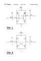
- a typical 6T cellillustrated in FIG. 1, consists of a latch made up of two cross coupled CMOS inverters, which form a circuit known as a flip-flop.
- the load devices Q 3 and Q 4are p-channel transistors.
- the pull down transistors, Q 5 and Q 6 , and the access transistors, Q 1 and Q 2are n-channel transistors.
- the term “pull down”derives from the fact that the output nodes of these transistors are pulled down to substantially ground potential when the transistors are biased to conduction.)
- the first access transistor Q 1the gate of which is controlled by word line WL, provides selective coupling of the true bit line D to storage node A.
- a second access transistor Q 2the gate of which is also controlled by word line WL, provides selective coupling of the complement bit line D′ to storage node B. Since very little power is required to maintain a latched state, 6T SRAMs are often used for memory in battery applications. 6T SRAMs are the most costly SRAMs to manufacture because the 6T cell uses the greatest amount of chip real estate.
- a typical 4T SRAM cell, illustrated in FIG. 2,is similar to the 6T cell of FIG. 1 except that the two p-channel load transistors are replaced by resistive elements, R 3 and R 4 .
- a 4T SRAMis usually less costly to produce than a 6T SRAM because more memory cells can be packed onto each chip. 4T SRAMs are, however, disadvantageous in very low power applications because the resistors consume more current than the p-channel transistors they replace.
- a three transistor (3T) SRAM memory cellwas developed.
- This new SRAM memory cellis described and claimed in my commonly owned and copending application Ser. No. 08/388,873, entitled “Three Transistor Static Random Access Memory Cell”, filed Feb. 14, 1995, incorporated herein by reference.
- the preferred embodiment of the 3T SRAM described in detail in this copending applicationcombines a DRAM memory cell with a half latch.
- That SRAM memory cell circuitryincludes an access transistor coupled to a capacitor, an n-channel pull down transistor and a p-channel thin film transistor (TFT) which acts as the capacitor pull up device.
- the gate of the TFTis formed in the same layer of polysilicon in which the capacitor storage node is formed.
- the source, drain and channel of the p-channel TFTis formed in a separate layer of polysilicon.
- the gate of the TFTis coupled to the supply voltage V cc through back to back diodes, which function as a resistor, and to ground or a substrate voltage through the pull down transistor.
- the present inventionis directed to a set of cross coupled thin film transistors that are formed on top of one another in vertically adjacent layers of polysilicon.
- This structural configurationsaves valuable chip real estate and, correspondingly, allows for reduced manufacturing costs
- the first TFTfunctions as the capacitor pull up device and the second TFT functions as an active load device in place of The back to back diodes described as part of the preferred embodiment in my copending application.
- Using a TFT instead of back to back diodes as the load deviceincreases the speed of read and write operations in the SRAM.
- the invented TFT cross coupling structureallows this increase in speed without adding to cell size.
- a pair of thin film transistorsformed in adjacent layers of polysilicon.
- the gate of the first TFT and the source, drain and channel regions of the second TFTare formed in the first polysilicon layer.
- the source, drain and channel regions of the first TFT and the gate of the second TFTare formed in the second polysilicon layer.
- a dielectric layeris interposed between the first and second polysilicon layers.
- the first TFT gateoverlaps the second TFT drain region in the first polysilicon layer and the second TFT gate overlaps the first TFT drain region in the second polysilicon layer.
- two TFTsare incorporated into a SRAM memory cell.
- the memory cellincludes: (i) a bit line; (ii) an access transistor having a first source/drain and a second source/drain, the first source/drain being electrically connected to the bit line; (iii) a parasitic diode formed between the second source/drain of the access transistor and the substrate; (iv) a pull down transistor having a source, drain, channel and gate; (v) a first TFT having a source, drain, channel and gate, the first TFT gate being coupled to a power supply voltage V cc through an active load device comprising a second TFT having a source, drain, channel and gate, and to a voltage not greater than ground through the pull down transistor; and (vi) a storage node for storing a high voltage representative of a first digital data state or a low voltage representative of a second digital state, the storage node being coupled to the bit line through the access transistor, to the substrate through the parasitic
- the first TFT gateis formed in a first polysilicon layer and the first TFT source, drain and channel are formed in a second polysilicon layer, the second polysilicon layer being disposed over and adjacent to the first polysilicon layer.
- the second TFT gateis formed in the second polysilicon layer and the second TFT source, drain and channel are formed in the first polysilicon layer.
- a dielectric layeris interposed between the first and second polysilicon layers.
- the first TFT gateoverlaps the second TFT source and the second TFT gate overlaps the first TFT source.
- FIG. 1is a schematic circuit diagram of a conventional 6T SRAM memory cell.
- FIG. 2is a schematic circuit diagram of a conventional 4T SRAM memory cell.
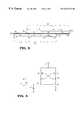
- FIG. 3is a cross section view illustrating the invented structural configuration of a pair of TFTs formed one on top of the other in vertically adjacent layers of polysilicon.
- FIG. 4is a schematic circuit diagram of a 4T SRAM memory cell constructed according to one of the preferred embodiments of the invention.
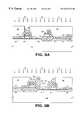
- FIG. 5is a top down plan view illustrating the preferred layout of the 4T cell of FIG. 4 .
- FIGS. 6A-10A and 6 B- 10 Bare cross section views illustrating sequentially the manufacture of the 4T memory cell of FIGS. 4 and 5.
- FIGS. 6A-10Aare taken along the line A-A′ in FIG. 5 .
- FIGS. 6B-10Bare taken along the line B-B′ in FIG. 5 .
- FIGS. 5-10are idealized representations used to depict the structure of the invention and the process steps used to form that structure. These figures are not meant to be actual views of an SRAM memory cell.
- a pair of cross coupled thin film transistors (TFTs) 22 , 24are formed one on top of the other in vertically adjacent layers of polysilicon 58 , 70 .
- First layer of polysilicon 58is deposited over a substrate structure and lightly doped with an n-type impurity such as phosphorus, arsenic or antimony.
- the source, drain and channel regions of the second TFT 24 , and the gate of the first TFT 22will be formed in first polysilicon layer 58 .
- the structureis then masked with an implant mask and the mask is patterned to expose first polysilicon layer 58 at the location of the source and drain for the second TFT 24 and the gate for the first TFT 22 .
- first polysilicon layer 58are heavily doped with a p-type impurity to form p+ drain region 62 and p+ source region 64 of second TFT 24 .
- Drain region 62 of second TFT 24also functions as the gate 65 of first TFT 22 .
- These implantsalso define the n- channel region 66 of second TFT 24 .
- a dielectric layer 68is formed over first polysilicon layer 44 .
- Dielectric layer 68consists of an oxide/nitride or oxide/nitride/oxide (“ONO”) film stack or a conventional gate material.
- a second layer of polysilicon 70is then deposited over the dielectric layer 68 and lightly doped with an n-type impurity.
- the source, drain and channel regions of the first TFT 22 , and the gate of the second TFT 24are formed in second polysilicon layer 68 .
- the arrayis masked with an implant mask and the mask is patterned to expose second polysilicon layer 70 at the location of the source and drain of the first TFT 22 and the gate of the second TFT 24 .
- second polysilicon layer 70are heavily doped with a p-type impurity to form p+ drain region 74 and p+source region 76 of first TFT 22 These implants define the n ⁇ channel region 79 of first TFT 22 .
- Drain region 74 of first TFTalso functions as the gate 78 of second TFT 24 .
- First and second TFTs 22 , 24are cross coupled via the overlapping/connecting drains 74 , 62 and gates 78 , 65 .
- the respective source regionswill be connected to a power supply voltage V cc and the gates will be cross coupled to drains of opposing n-channel transistors.
- FIG. 4is a schematic circuit diagram illustrating a novel 4T SRAM memory cell that uses the invented back to back TFTs.
- Insulated gate field effect access transistor 10provides bit line 12 with selective access to storage node 20 when word line 16 is brought to a high potential, typically 3-7 volts.
- storage node 20preferably consists of the parasitic capacitance inherent in the storage node polysilicon.
- storage node 20may be formed as a conventional DRAM “stacked” capacitor.
- the charge on the storage node 20leaks through a parasitic diode 18 formed at the junction of the storage node 20 and the substrate.
- the source of first thin film transistor (TFT) 22is electrically connected to the supply voltage V cc .
- the drain of first TFT 22is electrically connected to storage node 20 .
- the gate of first TFT 22is electrically connected to V cc through second TFT 24 and to ground through an insulated gate field effect pull down transistor 26
- the drain of pull down transistor 26is electrically connected to V cc through second TFT 24 , which serves as the active load for the pull down transistor 26 .
- the source of pull down transistor 26is electrically connected to ground.
- the gate of pull down transistor 26is electrically connected to storage node 20 .
- first TFT 22is never fully non-conductive because its channel is formed in a layer of polysilicon, the leakage through first TFT 22 is offset by the leakage through parasitic diode 18 which is set to be greater than the off-state current leakage through first TFT 22 when storage node 20 is discharged.
- the leakage of parasitic diode 18may be controlled by adjusting the doping profile of the storage node junction.
- FIGS. 6A-10A and 6 B- 10 Bare cross section views taken along the lines A-A′ and B-B′ in FIG. 5, respectively.
- Each of the cross section viewsmay represent a number of different individual process steps carried out to arrive at the particular structure shown. Since the individual process steps are conventional and well known to those skilled in the art of semiconductor device manufacturing, several of these steps have been combined in the various figures for the sake of simplicity and to better illustrate the preferred embodiment of the invented structures. Also, the fabrication of semiconductor devices includes etching predetermined patterns into layers of various material stacked over the semiconductor substrate.
- patterning and etchingThis process is sometimes referred to herein for convenience as “patterning and etching.” Photolithography and reactive ion etching, for example, are commonly used pattern and etch processes. These or other pattern and etch processes, well known to those skilled in the art, may be used to implement the present invention.
- wafer 30comprises a lightly doped p-type single crystal silicon substrate 32 which has been oxidized to form thin gate insulating layer 34 and thick field oxide regions 36 .
- Access transistor gate 40 and pull down transistor gate 42are formed by successively depositing or “stacking” a polysilicon layer 44 , a tungsten silicide layer 46 and a silicon dioxide layer 48 over substrate 32 , and then patterning and etching those layers to expose substrate 32 at desired locations of the transistor source/drain regions. These layers are deposited, patterned and etched using conventional methods well known in the art.
- transistor gates 40 and 42may be formed of a single layer of polysilicon deposited and etched as described above.
- tungsten silicide and silicon dioxide layersare included herein merely to better illustrate the details of the preferred embodiment of the invention.
- Impuritiesare implanted in the surface of substrate 32 to form n-doped source/drain regions 38 for access transistor 10 and pull down transistor 26 .
- the arrayis patterned and etched to remove a portion of the oxide layer on top of only the pull down transistor gate 42 . This insulating layer is removed from pull down transistor gate 42 so that contact can subsequently be made between gate 42 and storage node 20 .
- isolation oxide layer 50is formed over the entire array. Isolation oxide layer 50 is then patterned and etched to remove portions of oxide layer 50 from the storage node contact region 52 , landing pad 54 on the upper surface of the pull down transistor gate 42 , and the pull down transistor drain contact region 56 . A thin layer of highly conductive material 57 is then formed over the upper surface of the in process structure and patterned and etched to leave conductive material on the substrate in contact regions 38 . Conductive layer 57 will facilitate contact between n-regions 38 in substrate 32 and the subsequently formed p+ storage node polysilicon. Conductive layer 57 preferably consists of a transition refractory metal silicide or transition refractory metal nitride.
- Example transition metalsinclude tungsten (W), molybdenum (Mo), tantalum (Ta), titanium (Ti), protactinium (Pa), nickel (Ni) and cobalt (Co).
- the most preferred transition conductive materialis titanium nitride (TiN).
- a first layer of polysilicon 58is deposited over the array and lightly doped with an n-type impurity such as phosphorus, antimony or arsenic.
- First polysilicon layer 58is patterned and etched to form an “M” (turned on its side) shaped pattern as shown in FIG. 5 .
- the source, drain and channel regions of the second TFT 24 , and the gate of the first TFT 22will be formed in the first polysilicon layer 58 .
- the arrayis then masked with an implant mask 60 to expose first polysilicon layer 58 at the location of the source and drain for the second TFT 24 and the gate for the first TFT 22 .
- first polysilicon layer 58are heavily doped with a p-type impurity, indicated symbolically by implant arrows 61 , to form p+drain region 62 and source region 64 of second TFT 24 .
- Drain region 62 of second TFT 24also functions as the gate 65 of first TFT 22 .
- These implantsalso define the n-channel region 66 of second TFT 24 .
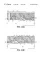
- Dielectric layer 68is formed over the array.
- Dielectric layer 68consists of an oxide/nitride or oxide/nitride/oxide (“ONO”) film stack or a conventional gate material.
- Dielectric layer 68is patterned and etched to expose substrate 32 at storage node contact region 52 and to expose landing pad 54 on pull down transistor gate 42 .
- a second layer of polysilicon 70is then deposited over the array and lightly doped with an n-type impurity. Second polysilicon layer 70 is patterned and etched to form a claw shaped pattern as shown in FIG. 5 .
- the source, drain and channel regions of the first TFT 22 , the gate of the second TFT 24 , and storage node 20are formed in second polysilicon layer 68 .
- the arrayis masked with an implant mask 72 to expose second polysilicon layer 70 at the location of the source and drain of the first TFT 22 , the gate of the second TFT 24 and storage node 20 .
- the exposed portions of second polysilicon layer 70are heavily doped with a p-type impurity, indicated symbolically by implant arrows 73 , to form p+ drain region 74 , source region 76 of first TFT 22 and storage node 20 . These implants define the n- channel region of first TFT 22 .
- Drain region 74 of first TFTalso functions as the gate 78 of second TFT 24 .
- the arrayis subjected to a light blanket p-type, peferably boron, implant to achieve the desired characteristics for second TFT gate 78 .
- a light blanket p-type, peferably boron, implantto achieve the desired characteristics for second TFT gate 78 .
- This and other conventional techniquesmay be used to optimize the TFT sub-threshold voltage characteristics and current drive/gain.
- the parasitic capacitance inherent in storage node 20can be made to hold a charge sufficient to maintain a high voltage (“1” value) in the cell.
- a conventional DRAM stacked capacitorcould be used as storage node 20 .
- the storage node(the capacitor bottom electrode) would be formed in the first polysilicon layer which would extend down to the substrate 32 at storage node contact region 52 .
- the cell plate(the capacitor top electrode) would thereafter be formed in the second polysilicon layer.
- a thick upper insulating layer 80 of boro-phospho-silicate glass (BPSG) or other suitable insulating materialis formed over the exposed upper surfaces of the structure previously formed.
- Upper insulating layer 80is patterned and etched to form a corridor down to substrate 32 .
- Bit line contact 82 and bit line 84are then formed using metal deposition techniques well known in the art.
Landscapes
- Engineering & Computer Science (AREA)
- Microelectronics & Electronic Packaging (AREA)
- Computer Hardware Design (AREA)
- Thin Film Transistor (AREA)
- Semiconductor Memories (AREA)
Abstract
Description
Claims (14)
Priority Applications (1)
| Application Number | Priority Date | Filing Date | Title |
|---|---|---|---|
| US09/136,902US6291276B1 (en) | 1995-11-20 | 1998-08-19 | Cross coupled thin film transistors and static random access memory cell |
Applications Claiming Priority (3)
| Application Number | Priority Date | Filing Date | Title |
|---|---|---|---|
| US08/561,131US5640342A (en) | 1995-11-20 | 1995-11-20 | Structure for cross coupled thin film transistors and static random access memory cell |
| US86801197A | 1997-06-03 | 1997-06-03 | |
| US09/136,902US6291276B1 (en) | 1995-11-20 | 1998-08-19 | Cross coupled thin film transistors and static random access memory cell |
Related Parent Applications (1)
| Application Number | Title | Priority Date | Filing Date |
|---|---|---|---|
| US86801197ADivision | 1995-11-20 | 1997-06-03 |
Publications (1)
| Publication Number | Publication Date |
|---|---|
| US6291276B1true US6291276B1 (en) | 2001-09-18 |
Family
ID=24240756
Family Applications (3)
| Application Number | Title | Priority Date | Filing Date |
|---|---|---|---|
| US08/561,131Expired - LifetimeUS5640342A (en) | 1995-11-20 | 1995-11-20 | Structure for cross coupled thin film transistors and static random access memory cell |
| US09/136,811Expired - LifetimeUS6054742A (en) | 1995-11-20 | 1998-08-19 | Structure for cross coupled thin film transistors and static random access memory cell |
| US09/136,902Expired - LifetimeUS6291276B1 (en) | 1995-11-20 | 1998-08-19 | Cross coupled thin film transistors and static random access memory cell |
Family Applications Before (2)
| Application Number | Title | Priority Date | Filing Date |
|---|---|---|---|
| US08/561,131Expired - LifetimeUS5640342A (en) | 1995-11-20 | 1995-11-20 | Structure for cross coupled thin film transistors and static random access memory cell |
| US09/136,811Expired - LifetimeUS6054742A (en) | 1995-11-20 | 1998-08-19 | Structure for cross coupled thin film transistors and static random access memory cell |
Country Status (1)
| Country | Link |
|---|---|
| US (3) | US5640342A (en) |
Cited By (23)
| Publication number | Priority date | Publication date | Assignee | Title |
|---|---|---|---|---|
| US6620672B1 (en)* | 2000-07-11 | 2003-09-16 | Micron Technology, Inc. | SOI DRAM with buried capacitor under the digit lines utilizing a self aligning penetrating storage node contact formation |
| US6751111B2 (en)* | 2000-03-03 | 2004-06-15 | Mosaid Technologies Incorporated | High density memory cell |
| US20100187627A1 (en)* | 2008-03-13 | 2010-07-29 | Tela Innovations, Inc. | Channelized Gate Level Cross-Coupled Transistor Device with Overlapping PMOS Transistors and Overlapping NMOS Transistors Relative to Direction of Gate Electrodes |
| US20110163365A1 (en)* | 2008-03-26 | 2011-07-07 | International Business Machines Corporation | Structure and method for improving storage latch susceptibility to single event upsets |
| US8448102B2 (en) | 2006-03-09 | 2013-05-21 | Tela Innovations, Inc. | Optimizing layout of irregular structures in regular layout context |
| US8453094B2 (en) | 2008-01-31 | 2013-05-28 | Tela Innovations, Inc. | Enforcement of semiconductor structure regularity for localized transistors and interconnect |
| US8471391B2 (en) | 2008-03-27 | 2013-06-25 | Tela Innovations, Inc. | Methods for multi-wire routing and apparatus implementing same |
| US8541879B2 (en) | 2007-12-13 | 2013-09-24 | Tela Innovations, Inc. | Super-self-aligned contacts and method for making the same |
| US8549455B2 (en) | 2007-08-02 | 2013-10-01 | Tela Innovations, Inc. | Methods for cell phasing and placement in dynamic array architecture and implementation of the same |
| US8653857B2 (en) | 2006-03-09 | 2014-02-18 | Tela Innovations, Inc. | Circuitry and layouts for XOR and XNOR logic |
| US8661392B2 (en) | 2009-10-13 | 2014-02-25 | Tela Innovations, Inc. | Methods for cell boundary encroachment and layouts implementing the Same |
| US8658542B2 (en) | 2006-03-09 | 2014-02-25 | Tela Innovations, Inc. | Coarse grid design methods and structures |
| US8667443B2 (en) | 2007-03-05 | 2014-03-04 | Tela Innovations, Inc. | Integrated circuit cell library for multiple patterning |
| US8680626B2 (en) | 2007-10-26 | 2014-03-25 | Tela Innovations, Inc. | Methods, structures, and designs for self-aligning local interconnects used in integrated circuits |
| US8756551B2 (en) | 2007-08-02 | 2014-06-17 | Tela Innovations, Inc. | Methods for designing semiconductor device with dynamic array section |
| US8823062B2 (en) | 2006-03-09 | 2014-09-02 | Tela Innovations, Inc. | Integrated circuit with offset line end spacings in linear gate electrode level |
| US8839175B2 (en) | 2006-03-09 | 2014-09-16 | Tela Innovations, Inc. | Scalable meta-data objects |
| US8863063B2 (en) | 2009-05-06 | 2014-10-14 | Tela Innovations, Inc. | Finfet transistor circuit |
| US9035359B2 (en) | 2006-03-09 | 2015-05-19 | Tela Innovations, Inc. | Semiconductor chip including region including linear-shaped conductive structures forming gate electrodes and having electrical connection areas arranged relative to inner region between transistors of different types and associated methods |
| US9122832B2 (en) | 2008-08-01 | 2015-09-01 | Tela Innovations, Inc. | Methods for controlling microloading variation in semiconductor wafer layout and fabrication |
| US9159627B2 (en) | 2010-11-12 | 2015-10-13 | Tela Innovations, Inc. | Methods for linewidth modification and apparatus implementing the same |
| US9230910B2 (en) | 2006-03-09 | 2016-01-05 | Tela Innovations, Inc. | Oversized contacts and vias in layout defined by linearly constrained topology |
| US9563733B2 (en) | 2009-05-06 | 2017-02-07 | Tela Innovations, Inc. | Cell circuit and layout with linear finfet structures |
Families Citing this family (46)
| Publication number | Priority date | Publication date | Assignee | Title |
|---|---|---|---|---|
| US5640342A (en) | 1995-11-20 | 1997-06-17 | Micron Technology, Inc. | Structure for cross coupled thin film transistors and static random access memory cell |
| US5716881A (en)* | 1996-03-28 | 1998-02-10 | Taiwan Semiconductor Manufacturing Company, Ltd. | Process to fabricate stacked capacitor DRAM and low power thin film transistor SRAM devices on a single semiconductor chip |
| US5830375A (en)* | 1996-06-10 | 1998-11-03 | Taiwan Semiconductor Manufacturing Company Ltd. | Automated method for monitoring and controlling the orthophosphoric acid etch rate of silicon nitride insulator layers |
| US5691230A (en) | 1996-09-04 | 1997-11-25 | Micron Technology, Inc. | Technique for producing small islands of silicon on insulator |
| US5838606A (en)* | 1997-04-28 | 1998-11-17 | Mitsubishi Semiconductor America, Inc. | Three-transistor static storage cell |
| US5909618A (en)* | 1997-07-08 | 1999-06-01 | Micron Technology, Inc. | Method of making memory cell with vertical transistor and buried word and body lines |
| US6191470B1 (en) | 1997-07-08 | 2001-02-20 | Micron Technology, Inc. | Semiconductor-on-insulator memory cell with buried word and body lines |
| US6072209A (en) | 1997-07-08 | 2000-06-06 | Micro Technology, Inc. | Four F2 folded bit line DRAM cell structure having buried bit and word lines |
| US5936274A (en)* | 1997-07-08 | 1999-08-10 | Micron Technology, Inc. | High density flash memory |
| US5973356A (en)* | 1997-07-08 | 1999-10-26 | Micron Technology, Inc. | Ultra high density flash memory |
| US6150687A (en) | 1997-07-08 | 2000-11-21 | Micron Technology, Inc. | Memory cell having a vertical transistor with buried source/drain and dual gates |
| US5914511A (en)* | 1997-10-06 | 1999-06-22 | Micron Technology, Inc. | Circuit and method for a folded bit line memory using trench plate capacitor cells with body bias contacts |
| US6066869A (en)* | 1997-10-06 | 2000-05-23 | Micron Technology, Inc. | Circuit and method for a folded bit line memory cell with vertical transistor and trench capacitor |
| US6528837B2 (en) | 1997-10-06 | 2003-03-04 | Micron Technology, Inc. | Circuit and method for an open bit line memory cell with a vertical transistor and trench plate trench capacitor |
| US5907170A (en)* | 1997-10-06 | 1999-05-25 | Micron Technology, Inc. | Circuit and method for an open bit line memory cell with a vertical transistor and trench plate trench capacitor |
| US6025225A (en)* | 1998-01-22 | 2000-02-15 | Micron Technology, Inc. | Circuits with a trench capacitor having micro-roughened semiconductor surfaces and methods for forming the same |
| US6304483B1 (en) | 1998-02-24 | 2001-10-16 | Micron Technology, Inc. | Circuits and methods for a static random access memory using vertical transistors |
| US6242775B1 (en) | 1998-02-24 | 2001-06-05 | Micron Technology, Inc. | Circuits and methods using vertical complementary transistors |
| US6246083B1 (en) | 1998-02-24 | 2001-06-12 | Micron Technology, Inc. | Vertical gain cell and array for a dynamic random access memory |
| US5963469A (en)* | 1998-02-24 | 1999-10-05 | Micron Technology, Inc. | Vertical bipolar read access for low voltage memory cell |
| US5991225A (en)* | 1998-02-27 | 1999-11-23 | Micron Technology, Inc. | Programmable memory address decode array with vertical transistors |
| US6124729A (en)* | 1998-02-27 | 2000-09-26 | Micron Technology, Inc. | Field programmable logic arrays with vertical transistors |
| US6043527A (en) | 1998-04-14 | 2000-03-28 | Micron Technology, Inc. | Circuits and methods for a memory cell with a trench plate trench capacitor and a vertical bipolar read device |
| US6208164B1 (en) | 1998-08-04 | 2001-03-27 | Micron Technology, Inc. | Programmable logic array with vertical transistors |
| US6134175A (en) | 1998-08-04 | 2000-10-17 | Micron Technology, Inc. | Memory address decode array with vertical transistors |
| US6093623A (en) | 1998-08-04 | 2000-07-25 | Micron Technology, Inc. | Methods for making silicon-on-insulator structures |
| US6423613B1 (en) | 1998-11-10 | 2002-07-23 | Micron Technology, Inc. | Low temperature silicon wafer bond process with bulk material bond strength |
| TW442837B (en)* | 1998-12-03 | 2001-06-23 | Infineon Technologies Ag | Integrated circuit-arrangement and its production method |
| JP4465743B2 (en)* | 1999-07-16 | 2010-05-19 | ソニー株式会社 | Semiconductor memory device |
| US6630718B1 (en)* | 1999-07-26 | 2003-10-07 | Micron Technology, Inc. | Transistor gate and local interconnect |
| US6496034B2 (en)* | 2001-02-09 | 2002-12-17 | Micron Technology, Inc. | Programmable logic arrays with ultra thin body transistors |
| US6531727B2 (en)* | 2001-02-09 | 2003-03-11 | Micron Technology, Inc. | Open bit line DRAM with ultra thin body transistors |
| US6566682B2 (en)* | 2001-02-09 | 2003-05-20 | Micron Technology, Inc. | Programmable memory address and decode circuits with ultra thin vertical body transistors |
| US6559491B2 (en)* | 2001-02-09 | 2003-05-06 | Micron Technology, Inc. | Folded bit line DRAM with ultra thin body transistors |
| US6424001B1 (en) | 2001-02-09 | 2002-07-23 | Micron Technology, Inc. | Flash memory with ultra thin vertical body transistors |
| US6442061B1 (en)* | 2001-02-14 | 2002-08-27 | Lsi Logic Corporation | Single channel four transistor SRAM |
| US6852167B2 (en) | 2001-03-01 | 2005-02-08 | Micron Technology, Inc. | Methods, systems, and apparatus for uniform chemical-vapor depositions |
| US6812529B2 (en)* | 2001-03-15 | 2004-11-02 | Micron Technology, Inc. | Suppression of cross diffusion and gate depletion |
| JP2003133417A (en)* | 2001-10-26 | 2003-05-09 | Matsushita Electric Ind Co Ltd | Semiconductor integrated circuit device and its design method |
| US7160577B2 (en) | 2002-05-02 | 2007-01-09 | Micron Technology, Inc. | Methods for atomic-layer deposition of aluminum oxides in integrated circuits |
| US7589029B2 (en) | 2002-05-02 | 2009-09-15 | Micron Technology, Inc. | Atomic layer deposition and conversion |
| US6649456B1 (en)* | 2002-10-16 | 2003-11-18 | Taiwan Semiconductor Manufacturing Company | SRAM cell design for soft error rate immunity |
| US6853579B1 (en)* | 2003-09-09 | 2005-02-08 | Taiwan Semiconductor Manufacturing Co., Ltd. | Non-refresh four-transistor memory cell |
| US7927948B2 (en) | 2005-07-20 | 2011-04-19 | Micron Technology, Inc. | Devices with nanocrystals and methods of formation |
| CN108806742B (en)* | 2017-05-04 | 2022-01-04 | 汤朝景 | Random access memory and having circuitry, methods and apparatus associated therewith |
| CN108321158B (en)* | 2018-04-11 | 2024-04-16 | 南京邮电大学 | Static random access memory unit based on photoelectric device and preparation method thereof |
Citations (10)
| Publication number | Priority date | Publication date | Assignee | Title |
|---|---|---|---|---|
| US5278459A (en) | 1990-11-15 | 1994-01-11 | Kabushiki Kaisha Toshiba | Static semiconductor memory using thin film FET |
| US5286663A (en) | 1992-01-29 | 1994-02-15 | Micron Technology, Inc. | Methods for producing thin film transistor having a diode shunt |
| US5388067A (en)* | 1993-04-01 | 1995-02-07 | Nec Corporation | Semiconductor memory cell |
| US5422499A (en) | 1993-02-22 | 1995-06-06 | Micron Semiconductor, Inc. | Sixteen megabit static random access memory (SRAM) cell |
| US5440508A (en) | 1994-02-09 | 1995-08-08 | Atmel Corporation | Zero power high speed programmable circuit device architecture |
| US5471071A (en)* | 1990-02-21 | 1995-11-28 | Sony Corporation | Semiconductor static random access memory structure |
| US5625200A (en)* | 1994-08-30 | 1997-04-29 | Lee; Kuo-Hua | Complementary TFT devices with diode-effect elimination means independent of TFT-channel geometry |
| US5640342A (en) | 1995-11-20 | 1997-06-17 | Micron Technology, Inc. | Structure for cross coupled thin film transistors and static random access memory cell |
| US5675185A (en)* | 1995-09-29 | 1997-10-07 | International Business Machines Corporation | Semiconductor structure incorporating thin film transistors with undoped cap oxide layers |
| US5818090A (en) | 1988-11-10 | 1998-10-06 | Seiko Epson Corporation | Semiconductor devices with load elements |
- 1995
- 1995-11-20USUS08/561,131patent/US5640342A/ennot_activeExpired - Lifetime
- 1998
- 1998-08-19USUS09/136,811patent/US6054742A/ennot_activeExpired - Lifetime
- 1998-08-19USUS09/136,902patent/US6291276B1/ennot_activeExpired - Lifetime
Patent Citations (10)
| Publication number | Priority date | Publication date | Assignee | Title |
|---|---|---|---|---|
| US5818090A (en) | 1988-11-10 | 1998-10-06 | Seiko Epson Corporation | Semiconductor devices with load elements |
| US5471071A (en)* | 1990-02-21 | 1995-11-28 | Sony Corporation | Semiconductor static random access memory structure |
| US5278459A (en) | 1990-11-15 | 1994-01-11 | Kabushiki Kaisha Toshiba | Static semiconductor memory using thin film FET |
| US5286663A (en) | 1992-01-29 | 1994-02-15 | Micron Technology, Inc. | Methods for producing thin film transistor having a diode shunt |
| US5422499A (en) | 1993-02-22 | 1995-06-06 | Micron Semiconductor, Inc. | Sixteen megabit static random access memory (SRAM) cell |
| US5388067A (en)* | 1993-04-01 | 1995-02-07 | Nec Corporation | Semiconductor memory cell |
| US5440508A (en) | 1994-02-09 | 1995-08-08 | Atmel Corporation | Zero power high speed programmable circuit device architecture |
| US5625200A (en)* | 1994-08-30 | 1997-04-29 | Lee; Kuo-Hua | Complementary TFT devices with diode-effect elimination means independent of TFT-channel geometry |
| US5675185A (en)* | 1995-09-29 | 1997-10-07 | International Business Machines Corporation | Semiconductor structure incorporating thin film transistors with undoped cap oxide layers |
| US5640342A (en) | 1995-11-20 | 1997-06-17 | Micron Technology, Inc. | Structure for cross coupled thin film transistors and static random access memory cell |
Cited By (113)
| Publication number | Priority date | Publication date | Assignee | Title |
|---|---|---|---|---|
| US6751111B2 (en)* | 2000-03-03 | 2004-06-15 | Mosaid Technologies Incorporated | High density memory cell |
| US6620672B1 (en)* | 2000-07-11 | 2003-09-16 | Micron Technology, Inc. | SOI DRAM with buried capacitor under the digit lines utilizing a self aligning penetrating storage node contact formation |
| US9859277B2 (en) | 2006-03-09 | 2018-01-02 | Tela Innovations, Inc. | Methods, structures, and designs for self-aligning local interconnects used in integrated circuits |
| US9754878B2 (en) | 2006-03-09 | 2017-09-05 | Tela Innovations, Inc. | Semiconductor chip including a chip level based on a layout that includes both regular and irregular wires |
| US10230377B2 (en) | 2006-03-09 | 2019-03-12 | Tela Innovations, Inc. | Circuitry and layouts for XOR and XNOR logic |
| US8448102B2 (en) | 2006-03-09 | 2013-05-21 | Tela Innovations, Inc. | Optimizing layout of irregular structures in regular layout context |
| US10217763B2 (en) | 2006-03-09 | 2019-02-26 | Tela Innovations, Inc. | Semiconductor chip having region including gate electrode features of rectangular shape on gate horizontal grid and first-metal structures of rectangular shape on at least eight first-metal gridlines of first-metal vertical grid |
| US10186523B2 (en) | 2006-03-09 | 2019-01-22 | Tela Innovations, Inc. | Semiconductor chip having region including gate electrode features formed in part from rectangular layout shapes on gate horizontal grid and first-metal structures formed in part from rectangular layout shapes on at least eight first-metal gridlines of first-metal vertical grid |
| US8839175B2 (en) | 2006-03-09 | 2014-09-16 | Tela Innovations, Inc. | Scalable meta-data objects |
| US8952425B2 (en) | 2006-03-09 | 2015-02-10 | Tela Innovations, Inc. | Integrated circuit including at least four linear-shaped conductive structures having extending portions of different length |
| US10141334B2 (en) | 2006-03-09 | 2018-11-27 | Tela Innovations, Inc. | Semiconductor chip including region having rectangular-shaped gate structures and first-metal structures |
| US10141335B2 (en) | 2006-03-09 | 2018-11-27 | Tela Innovations, Inc. | Semiconductor CIP including region having rectangular-shaped gate structures and first metal structures |
| US8823062B2 (en) | 2006-03-09 | 2014-09-02 | Tela Innovations, Inc. | Integrated circuit with offset line end spacings in linear gate electrode level |
| US9917056B2 (en) | 2006-03-09 | 2018-03-13 | Tela Innovations, Inc. | Coarse grid design methods and structures |
| US9009641B2 (en) | 2006-03-09 | 2015-04-14 | Tela Innovations, Inc. | Circuits with linear finfet structures |
| US9905576B2 (en) | 2006-03-09 | 2018-02-27 | Tela Innovations, Inc. | Semiconductor chip including region having rectangular-shaped gate structures and first metal structures |
| US8946781B2 (en) | 2006-03-09 | 2015-02-03 | Tela Innovations, Inc. | Integrated circuit including gate electrode conductive structures with different extension distances beyond contact |
| US9425272B2 (en) | 2006-03-09 | 2016-08-23 | Tela Innovations, Inc. | Semiconductor chip including integrated circuit including four transistors of first transistor type and four transistors of second transistor type with electrical connections between various transistors and methods for manufacturing the same |
| US9711495B2 (en) | 2006-03-09 | 2017-07-18 | Tela Innovations, Inc. | Oversized contacts and vias in layout defined by linearly constrained topology |
| US9741719B2 (en) | 2006-03-09 | 2017-08-22 | Tela Innovations, Inc. | Methods, structures, and designs for self-aligning local interconnects used in integrated circuits |
| US9035359B2 (en) | 2006-03-09 | 2015-05-19 | Tela Innovations, Inc. | Semiconductor chip including region including linear-shaped conductive structures forming gate electrodes and having electrical connection areas arranged relative to inner region between transistors of different types and associated methods |
| US8653857B2 (en) | 2006-03-09 | 2014-02-18 | Tela Innovations, Inc. | Circuitry and layouts for XOR and XNOR logic |
| US9673825B2 (en) | 2006-03-09 | 2017-06-06 | Tela Innovations, Inc. | Circuitry and layouts for XOR and XNOR logic |
| US8658542B2 (en) | 2006-03-09 | 2014-02-25 | Tela Innovations, Inc. | Coarse grid design methods and structures |
| US8921896B2 (en) | 2006-03-09 | 2014-12-30 | Tela Innovations, Inc. | Integrated circuit including linear gate electrode structures having different extension distances beyond contact |
| US9230910B2 (en) | 2006-03-09 | 2016-01-05 | Tela Innovations, Inc. | Oversized contacts and vias in layout defined by linearly constrained topology |
| US9240413B2 (en) | 2006-03-09 | 2016-01-19 | Tela Innovations, Inc. | Methods, structures, and designs for self-aligning local interconnects used in integrated circuits |
| US9589091B2 (en) | 2006-03-09 | 2017-03-07 | Tela Innovations, Inc. | Scalable meta-data objects |
| US9336344B2 (en) | 2006-03-09 | 2016-05-10 | Tela Innovations, Inc. | Coarse grid design methods and structures |
| US8921897B2 (en) | 2006-03-09 | 2014-12-30 | Tela Innovations, Inc. | Integrated circuit with gate electrode conductive structures having offset ends |
| US9443947B2 (en) | 2006-03-09 | 2016-09-13 | Tela Innovations, Inc. | Semiconductor chip including region having integrated circuit transistor gate electrodes formed by various conductive structures of specified shape and position and method for manufacturing the same |
| US9425145B2 (en) | 2006-03-09 | 2016-08-23 | Tela Innovations, Inc. | Oversized contacts and vias in layout defined by linearly constrained topology |
| US9425273B2 (en) | 2006-03-09 | 2016-08-23 | Tela Innovations, Inc. | Semiconductor chip including integrated circuit including at least five gate level conductive structures having particular spatial and electrical relationship and method for manufacturing the same |
| US8667443B2 (en) | 2007-03-05 | 2014-03-04 | Tela Innovations, Inc. | Integrated circuit cell library for multiple patterning |
| US9633987B2 (en) | 2007-03-05 | 2017-04-25 | Tela Innovations, Inc. | Integrated circuit cell library for multiple patterning |
| US10074640B2 (en) | 2007-03-05 | 2018-09-11 | Tela Innovations, Inc. | Integrated circuit cell library for multiple patterning |
| US8966424B2 (en) | 2007-03-07 | 2015-02-24 | Tela Innovations, Inc. | Methods for cell phasing and placement in dynamic array architecture and implementation of the same |
| US9910950B2 (en) | 2007-03-07 | 2018-03-06 | Tela Innovations, Inc. | Methods for cell phasing and placement in dynamic array architecture and implementation of the same |
| US9424387B2 (en) | 2007-03-07 | 2016-08-23 | Tela Innovations, Inc. | Methods for cell phasing and placement in dynamic array architecture and implementation of the same |
| US9595515B2 (en) | 2007-03-07 | 2017-03-14 | Tela Innovations, Inc. | Semiconductor chip including integrated circuit defined within dynamic array section |
| US8759882B2 (en) | 2007-08-02 | 2014-06-24 | Tela Innovations, Inc. | Semiconductor device with dynamic array sections defined and placed according to manufacturing assurance halos |
| US8756551B2 (en) | 2007-08-02 | 2014-06-17 | Tela Innovations, Inc. | Methods for designing semiconductor device with dynamic array section |
| US8549455B2 (en) | 2007-08-02 | 2013-10-01 | Tela Innovations, Inc. | Methods for cell phasing and placement in dynamic array architecture and implementation of the same |
| US8680626B2 (en) | 2007-10-26 | 2014-03-25 | Tela Innovations, Inc. | Methods, structures, and designs for self-aligning local interconnects used in integrated circuits |
| US10734383B2 (en) | 2007-10-26 | 2020-08-04 | Tela Innovations, Inc. | Methods, structures, and designs for self-aligning local interconnects used in integrated circuits |
| US9818747B2 (en) | 2007-12-13 | 2017-11-14 | Tela Innovations, Inc. | Super-self-aligned contacts and method for making the same |
| US9281371B2 (en) | 2007-12-13 | 2016-03-08 | Tela Innovations, Inc. | Super-self-aligned contacts and method for making the same |
| US8541879B2 (en) | 2007-12-13 | 2013-09-24 | Tela Innovations, Inc. | Super-self-aligned contacts and method for making the same |
| US8951916B2 (en) | 2007-12-13 | 2015-02-10 | Tela Innovations, Inc. | Super-self-aligned contacts and method for making the same |
| US10461081B2 (en) | 2007-12-13 | 2019-10-29 | Tel Innovations, Inc. | Super-self-aligned contacts and method for making the same |
| US8701071B2 (en) | 2008-01-31 | 2014-04-15 | Tela Innovations, Inc. | Enforcement of semiconductor structure regularity for localized transistors and interconnect |
| US9202779B2 (en) | 2008-01-31 | 2015-12-01 | Tela Innovations, Inc. | Enforcement of semiconductor structure regularity for localized transistors and interconnect |
| US8453094B2 (en) | 2008-01-31 | 2013-05-28 | Tela Innovations, Inc. | Enforcement of semiconductor structure regularity for localized transistors and interconnect |
| US9530734B2 (en) | 2008-01-31 | 2016-12-27 | Tela Innovations, Inc. | Enforcement of semiconductor structure regularity for localized transistors and interconnect |
| US8729606B2 (en) | 2008-03-13 | 2014-05-20 | Tela Innovations, Inc. | Integrated circuit including cross-coupled transistors having gate electrodes formed within gate level feature layout channels |
| US8581304B2 (en) | 2008-03-13 | 2013-11-12 | Tela Innovations, Inc. | Integrated circuit including cross-coupled transistors having gate electrodes formed within gate level feature layout channels with four inside positioned gate contacts having offset and aligned relationships |
| US8847329B2 (en) | 2008-03-13 | 2014-09-30 | Tela Innovations, Inc. | Cross-coupled transistor circuit defined having diffusion regions of common node on opposing sides of same gate electrode track with at least two non-inner positioned gate contacts |
| US8847331B2 (en) | 2008-03-13 | 2014-09-30 | Tela Innovations, Inc. | Semiconductor chip including region having cross-coupled transistor configuration with offset electrical connection areas on gate electrode forming conductive structures and at least two different inner extension distances of gate electrode forming conductive structures |
| US8836045B2 (en) | 2008-03-13 | 2014-09-16 | Tela Innovations, Inc. | Cross-coupled transistor circuit having diffusion regions of common node on opposing sides of same gate electrode track |
| US8835989B2 (en) | 2008-03-13 | 2014-09-16 | Tela Innovations, Inc. | Integrated circuit including cross-coupled transistors having gate electrodes formed within gate level feature layout channels with gate electrode placement specifications |
| US8816402B2 (en) | 2008-03-13 | 2014-08-26 | Tela Innovations, Inc. | Integrated circuit including cross-coupled transistors having gate electrodes formed within gate level feature layout channels with gate level feature layout channel including single transistor |
| US8785979B2 (en) | 2008-03-13 | 2014-07-22 | Tela Innovations, Inc. | Integrated circuit including cross-coupled transistors having gate electrodes formed within gate level feature layout channels with two inside positioned gate contacts and two outside positioned gate contacts and electrical connection of cross-coupled transistors through same interconnect layer |
| US9081931B2 (en) | 2008-03-13 | 2015-07-14 | Tela Innovations, Inc. | Cross-coupled transistor circuit having diffusion regions of common node on opposing sides of same gate electrode track and gate node connection through single interconnect layer |
| US9117050B2 (en) | 2008-03-13 | 2015-08-25 | Tela Innovations, Inc. | Integrated circuit including cross-coupled transistors having gate electrodes formed within gate level feature layout channels with gate contact position and offset specifications |
| US20100187627A1 (en)* | 2008-03-13 | 2010-07-29 | Tela Innovations, Inc. | Channelized Gate Level Cross-Coupled Transistor Device with Overlapping PMOS Transistors and Overlapping NMOS Transistors Relative to Direction of Gate Electrodes |
| US10727252B2 (en) | 2008-03-13 | 2020-07-28 | Tela Innovations, Inc. | Semiconductor chip including integrated circuit having cross-coupled transistor configuration and method for manufacturing the same |
| US8853793B2 (en) | 2008-03-13 | 2014-10-07 | Tela Innovations, Inc. | Integrated circuit including gate electrode level region including cross-coupled transistors having gate contacts located over inner portion of gate electrode level region and offset gate level feature line ends |
| US9208279B2 (en) | 2008-03-13 | 2015-12-08 | Tela Innovations, Inc. | Semiconductor chip including digital logic circuit including linear-shaped conductive structures having electrical connection areas located within inner region between transistors of different type and associated methods |
| US9213792B2 (en) | 2008-03-13 | 2015-12-15 | Tela Innovations, Inc. | Semiconductor chip including digital logic circuit including at least six transistors with some transistors forming cross-coupled transistor configuration and associated methods |
| US8785978B2 (en) | 2008-03-13 | 2014-07-22 | Tela Innovations, Inc. | Integrated circuit including cross-coupled transistors having gate electrodes formed within gate level feature layout channels with electrical connection of cross-coupled transistors through same interconnect layer |
| US8772839B2 (en) | 2008-03-13 | 2014-07-08 | Tela Innovations, Inc. | Integrated circuit including cross-coupled transistors having gate electrodes formed within gate level feature layout channels with four inside positioned gate contacts having offset and aligned relationships and electrical connection of transistor gates through linear interconnect conductors in single interconnect layer |
| US9245081B2 (en) | 2008-03-13 | 2016-01-26 | Tela Innovations, Inc. | Semiconductor chip including digital logic circuit including at least nine linear-shaped conductive structures collectively forming gate electrodes of at least six transistors with some transistors forming cross-coupled transistor configuration and associated methods |
| US10658385B2 (en) | 2008-03-13 | 2020-05-19 | Tela Innovations, Inc. | Cross-coupled transistor circuit defined on four gate electrode tracks |
| US10651200B2 (en) | 2008-03-13 | 2020-05-12 | Tela Innovations, Inc. | Cross-coupled transistor circuit defined on three gate electrode tracks |
| US8742462B2 (en) | 2008-03-13 | 2014-06-03 | Tela Innovations, Inc. | Integrated circuit including cross-coupled transistors having gate electrodes formed within gate level feature layout channels with gate contact position specifications |
| US8866197B2 (en) | 2008-03-13 | 2014-10-21 | Tela Innovations, Inc. | Integrated circuit including cross-coupled transistors having gate electrodes formed within gate level feature layout channels with at least two gate electrodes electrically connected to each other through another transistor forming gate level feature |
| US8742463B2 (en) | 2008-03-13 | 2014-06-03 | Tela Innovations, Inc. | Integrated circuit including cross-coupled transistors having gate electrodes formed within gate level feature layout channels with outer positioned gate contacts |
| US8735995B2 (en) | 2008-03-13 | 2014-05-27 | Tela Innovations, Inc. | Cross-coupled transistor circuit defined on three gate electrode tracks with diffusion regions of common node on opposing sides of same gate electrode track |
| US8735944B2 (en) | 2008-03-13 | 2014-05-27 | Tela Innovations, Inc. | Integrated circuit including cross-coupled transistors having gate electrodes formed within gate level feature layout channels with serially connected transistors |
| US8729643B2 (en) | 2008-03-13 | 2014-05-20 | Tela Innovations, Inc. | Cross-coupled transistor circuit including offset inner gate contacts |
| US8552508B2 (en) | 2008-03-13 | 2013-10-08 | Tela Innovations, Inc. | Integrated circuit including cross-coupled transistors having gate electrodes formed within gate level feature layout channels with shared diffusion regions on opposite sides of two-transistor-forming gate level feature and electrical connection of transistor gates through linear interconnect conductors in single interconnect layer |
| US8872283B2 (en) | 2008-03-13 | 2014-10-28 | Tela Innovations, Inc. | Integrated circuit including cross-coupled transistors having gate electrodes formed within gate level feature layout channels with shared diffusion regions on opposite sides of two-transistor-forming gate level feature |
| US8853794B2 (en) | 2008-03-13 | 2014-10-07 | Tela Innovations, Inc. | Integrated circuit within semiconductor chip including cross-coupled transistor configuration |
| US8552509B2 (en) | 2008-03-13 | 2013-10-08 | Tela Innovations, Inc. | Integrated circuit including cross-coupled transistors having gate electrodes formed within gate level feature layout channels with other transistors positioned between cross-coupled transistors |
| US8575706B2 (en) | 2008-03-13 | 2013-11-05 | Tela Innovations, Inc. | Integrated circuit including cross-coupled transistors having gate electrodes formed within gate level feature layout channels with at least two different gate level features inner extensions beyond gate electrode |
| US8680583B2 (en) | 2008-03-13 | 2014-03-25 | Tela Innovations, Inc. | Integrated circuit including cross-coupled transistors having gate electrodes formed within at least nine gate level feature layout channels |
| US8669594B2 (en) | 2008-03-13 | 2014-03-11 | Tela Innovations, Inc. | Integrated circuit including cross-coupled transistors having gate electrodes formed within at least twelve gate level feature layout channels |
| US8669595B2 (en) | 2008-03-13 | 2014-03-11 | Tela Innovations, Inc. | Integrated circuit including cross-coupled transistors having gate electrodes formed within gate level feature layout channels with gate contact position, alignment, and offset specifications |
| US8558322B2 (en) | 2008-03-13 | 2013-10-15 | Tela Innovations, Inc. | Integrated circuit including cross-coupled transistors having gate electrodes formed within gate level feature layout channels with at least two gate electrodes electrically connected to each other through gate level feature |
| US10020321B2 (en) | 2008-03-13 | 2018-07-10 | Tela Innovations, Inc. | Cross-coupled transistor circuit defined on two gate electrode tracks |
| US8592872B2 (en) | 2008-03-13 | 2013-11-26 | Tela Innovations, Inc. | Integrated circuit including cross-coupled transistors with two transistors of different type having gate electrodes formed by common gate level feature with shared diffusion regions on opposite sides of common gate level feature |
| TWI416710B (en)* | 2008-03-13 | 2013-11-21 | Tela Innovations Inc | Limiting the cross-coupling transistor layout in the logic gate layout architecture |
| US8587034B2 (en) | 2008-03-13 | 2013-11-19 | Tela Innovations, Inc. | Integrated circuit including cross-coupled transistors having gate electrodes formed within gate level feature layout channels with four inside positioned gate contacts and electrical connection of transistor gates through linear interconnect conductors in single interconnect layer |
| US8564071B2 (en) | 2008-03-13 | 2013-10-22 | Tela Innovations, Inc. | Integrated circuit including cross-coupled transistors having gate electrodes formed within gate level feature layout channels with at least two different gate level feature extensions beyond contact |
| US9536899B2 (en) | 2008-03-13 | 2017-01-03 | Tela Innovations, Inc. | Semiconductor chip including integrated circuit having cross-coupled transistor configuration and method for manufacturing the same |
| US8581303B2 (en) | 2008-03-13 | 2013-11-12 | Tela Innovations, Inc. | Integrated circuit including cross-coupled trasistors having gate electrodes formed within gate level feature layout channels with four inside positioned gate contacts having offset relationships and electrical connection of cross-coupled transistors through same interconnect layer |
| US9871056B2 (en) | 2008-03-13 | 2018-01-16 | Tela Innovations, Inc. | Semiconductor chip including integrated circuit having cross-coupled transistor configuration and method for manufacturing the same |
| US8569841B2 (en) | 2008-03-13 | 2013-10-29 | Tela Innovations, Inc. | Integrated circuit including cross-coupled transistors having gate electrodes formed within gate level feature layout channels with at least one gate level feature extending into adjacent gate level feature layout channel |
| US20110163365A1 (en)* | 2008-03-26 | 2011-07-07 | International Business Machines Corporation | Structure and method for improving storage latch susceptibility to single event upsets |
| US8300452B2 (en)* | 2008-03-26 | 2012-10-30 | International Business Machines Corporation | Structure and method for improving storage latch susceptibility to single event upsets |
| US9390215B2 (en) | 2008-03-27 | 2016-07-12 | Tela Innovations, Inc. | Methods for multi-wire routing and apparatus implementing same |
| US9779200B2 (en) | 2008-03-27 | 2017-10-03 | Tela Innovations, Inc. | Methods for multi-wire routing and apparatus implementing same |
| US8759985B2 (en) | 2008-03-27 | 2014-06-24 | Tela Innovations, Inc. | Methods for multi-wire routing and apparatus implementing same |
| US8471391B2 (en) | 2008-03-27 | 2013-06-25 | Tela Innovations, Inc. | Methods for multi-wire routing and apparatus implementing same |
| US9122832B2 (en) | 2008-08-01 | 2015-09-01 | Tela Innovations, Inc. | Methods for controlling microloading variation in semiconductor wafer layout and fabrication |
| US10446536B2 (en) | 2009-05-06 | 2019-10-15 | Tela Innovations, Inc. | Cell circuit and layout with linear finfet structures |
| US9563733B2 (en) | 2009-05-06 | 2017-02-07 | Tela Innovations, Inc. | Cell circuit and layout with linear finfet structures |
| US8863063B2 (en) | 2009-05-06 | 2014-10-14 | Tela Innovations, Inc. | Finfet transistor circuit |
| US9530795B2 (en) | 2009-10-13 | 2016-12-27 | Tela Innovations, Inc. | Methods for cell boundary encroachment and semiconductor devices implementing the same |
| US8661392B2 (en) | 2009-10-13 | 2014-02-25 | Tela Innovations, Inc. | Methods for cell boundary encroachment and layouts implementing the Same |
| US9269702B2 (en) | 2009-10-13 | 2016-02-23 | Tela Innovations, Inc. | Methods for cell boundary encroachment and layouts implementing the same |
| US9159627B2 (en) | 2010-11-12 | 2015-10-13 | Tela Innovations, Inc. | Methods for linewidth modification and apparatus implementing the same |
| US9704845B2 (en) | 2010-11-12 | 2017-07-11 | Tela Innovations, Inc. | Methods for linewidth modification and apparatus implementing the same |
Also Published As
| Publication number | Publication date |
|---|---|
| US6054742A (en) | 2000-04-25 |
| US5640342A (en) | 1997-06-17 |
Similar Documents
| Publication | Publication Date | Title |
|---|---|---|
| US6291276B1 (en) | Cross coupled thin film transistors and static random access memory cell | |
| US5057898A (en) | Double-gated semiconductor memory device | |
| US5744846A (en) | SRAM cell employing substantially vertically elongated pull-up resistors and methods of making, and resistor constructions and methods of making | |
| US6468855B2 (en) | Reduced topography DRAM cell fabricated using a modified logic process and method for operating same | |
| US4675715A (en) | Semiconductor integrated circuit vertical geometry impedance element | |
| JP4316884B2 (en) | DRAM cell having capacitor structure partially manufactured in cavity and method of manufacturing the same | |
| US5198683A (en) | Integrated circuit memory device and structural layout thereof | |
| US4987090A (en) | Static ram cell with trench pull-down transistors and buried-layer ground plate | |
| KR100253032B1 (en) | Semiconductor memory device having static random access memory | |
| EP0460833B1 (en) | Method of fabricating a field effect device with polycrystaline silicon channel | |
| JP3089570B2 (en) | Integrated circuit comprising a plurality of transistor structures with shared electrodes | |
| JPH0644392B2 (en) | Method of manufacturing memory cell | |
| JPH06151772A (en) | SRAM having dual vertical channels and method of manufacturing the same | |
| US6008080A (en) | Method of making a low power SRAM | |
| US5572461A (en) | Static random access memory cell having a capacitor and a capacitor charge maintenance circuit | |
| US5592011A (en) | Single layer thin film transistor static random access memory cell | |
| US6009010A (en) | Static semiconductor memory device having data lines in parallel with power supply lines | |
| US5691217A (en) | Semiconductor processing method of forming a pair of field effect transistors having different thickness gate dielectric layers | |
| US6509595B1 (en) | DRAM cell fabricated using a modified logic process and method for operating same | |
| US5721163A (en) | Method of manufacture of thin film transistor SRAM device with a titanium nitride or silicide gate | |
| KR100319623B1 (en) | Dram cell array and fabrication method thereof | |
| US5761113A (en) | Soft error suppressing resistance load type SRAM cell | |
| US6563177B2 (en) | Semiconductor memory device having a trench and a gate electrode vertically formed on a wall of the trench | |
| JPH1050865A (en) | High-resistance loaded sram cell and method of manufacturing the same | |
| KR100273504B1 (en) | Semiconductor memory device, method of manufacturing the same, and method of use |
Legal Events
| Date | Code | Title | Description |
|---|---|---|---|
| STCF | Information on status: patent grant | Free format text:PATENTED CASE | |
| FPAY | Fee payment | Year of fee payment:4 | |
| FPAY | Fee payment | Year of fee payment:8 | |
| FPAY | Fee payment | Year of fee payment:12 | |
| AS | Assignment | Owner name:U.S. BANK NATIONAL ASSOCIATION, AS COLLATERAL AGENT, CALIFORNIA Free format text:SECURITY INTEREST;ASSIGNOR:MICRON TECHNOLOGY, INC.;REEL/FRAME:038669/0001 Effective date:20160426 Owner name:U.S. BANK NATIONAL ASSOCIATION, AS COLLATERAL AGEN Free format text:SECURITY INTEREST;ASSIGNOR:MICRON TECHNOLOGY, INC.;REEL/FRAME:038669/0001 Effective date:20160426 | |
| AS | Assignment | Owner name:MORGAN STANLEY SENIOR FUNDING, INC., AS COLLATERAL AGENT, MARYLAND Free format text:PATENT SECURITY AGREEMENT;ASSIGNOR:MICRON TECHNOLOGY, INC.;REEL/FRAME:038954/0001 Effective date:20160426 Owner name:MORGAN STANLEY SENIOR FUNDING, INC., AS COLLATERAL Free format text:PATENT SECURITY AGREEMENT;ASSIGNOR:MICRON TECHNOLOGY, INC.;REEL/FRAME:038954/0001 Effective date:20160426 | |
| AS | Assignment | Owner name:U.S. BANK NATIONAL ASSOCIATION, AS COLLATERAL AGENT, CALIFORNIA Free format text:CORRECTIVE ASSIGNMENT TO CORRECT THE REPLACE ERRONEOUSLY FILED PATENT #7358718 WITH THE CORRECT PATENT #7358178 PREVIOUSLY RECORDED ON REEL 038669 FRAME 0001. ASSIGNOR(S) HEREBY CONFIRMS THE SECURITY INTEREST;ASSIGNOR:MICRON TECHNOLOGY, INC.;REEL/FRAME:043079/0001 Effective date:20160426 Owner name:U.S. BANK NATIONAL ASSOCIATION, AS COLLATERAL AGEN Free format text:CORRECTIVE ASSIGNMENT TO CORRECT THE REPLACE ERRONEOUSLY FILED PATENT #7358718 WITH THE CORRECT PATENT #7358178 PREVIOUSLY RECORDED ON REEL 038669 FRAME 0001. ASSIGNOR(S) HEREBY CONFIRMS THE SECURITY INTEREST;ASSIGNOR:MICRON TECHNOLOGY, INC.;REEL/FRAME:043079/0001 Effective date:20160426 | |
| AS | Assignment | Owner name:JPMORGAN CHASE BANK, N.A., AS COLLATERAL AGENT, ILLINOIS Free format text:SECURITY INTEREST;ASSIGNORS:MICRON TECHNOLOGY, INC.;MICRON SEMICONDUCTOR PRODUCTS, INC.;REEL/FRAME:047540/0001 Effective date:20180703 Owner name:JPMORGAN CHASE BANK, N.A., AS COLLATERAL AGENT, IL Free format text:SECURITY INTEREST;ASSIGNORS:MICRON TECHNOLOGY, INC.;MICRON SEMICONDUCTOR PRODUCTS, INC.;REEL/FRAME:047540/0001 Effective date:20180703 | |
| AS | Assignment | Owner name:MICRON TECHNOLOGY, INC., IDAHO Free format text:RELEASE BY SECURED PARTY;ASSIGNOR:U.S. BANK NATIONAL ASSOCIATION, AS COLLATERAL AGENT;REEL/FRAME:047243/0001 Effective date:20180629 | |
| AS | Assignment | Owner name:MICRON TECHNOLOGY, INC., IDAHO Free format text:RELEASE BY SECURED PARTY;ASSIGNOR:MORGAN STANLEY SENIOR FUNDING, INC., AS COLLATERAL AGENT;REEL/FRAME:050937/0001 Effective date:20190731 | |
| AS | Assignment | Owner name:MICRON TECHNOLOGY, INC., IDAHO Free format text:RELEASE BY SECURED PARTY;ASSIGNOR:JPMORGAN CHASE BANK, N.A., AS COLLATERAL AGENT;REEL/FRAME:051028/0001 Effective date:20190731 Owner name:MICRON SEMICONDUCTOR PRODUCTS, INC., IDAHO Free format text:RELEASE BY SECURED PARTY;ASSIGNOR:JPMORGAN CHASE BANK, N.A., AS COLLATERAL AGENT;REEL/FRAME:051028/0001 Effective date:20190731 |