US6291082B1 - Method of electroless ag layer formation for cu interconnects - Google Patents
Method of electroless ag layer formation for cu interconnectsDownload PDFInfo
- Publication number
- US6291082B1 US6291082B1US09/592,164US59216400AUS6291082B1US 6291082 B1US6291082 B1US 6291082B1US 59216400 AUS59216400 AUS 59216400AUS 6291082 B1US6291082 B1US 6291082B1
- Authority
- US
- United States
- Prior art keywords
- layer
- silver
- copper
- opening
- dielectric
- Prior art date
- Legal status (The legal status is an assumption and is not a legal conclusion. Google has not performed a legal analysis and makes no representation as to the accuracy of the status listed.)
- Expired - Lifetime
Links
Images


Classifications
- H—ELECTRICITY
- H01—ELECTRIC ELEMENTS
- H01L—SEMICONDUCTOR DEVICES NOT COVERED BY CLASS H10
- H01L23/00—Details of semiconductor or other solid state devices
- H01L23/52—Arrangements for conducting electric current within the device in operation from one component to another, i.e. interconnections, e.g. wires, lead frames
- H01L23/522—Arrangements for conducting electric current within the device in operation from one component to another, i.e. interconnections, e.g. wires, lead frames including external interconnections consisting of a multilayer structure of conductive and insulating layers inseparably formed on the semiconductor body
- H01L23/532—Arrangements for conducting electric current within the device in operation from one component to another, i.e. interconnections, e.g. wires, lead frames including external interconnections consisting of a multilayer structure of conductive and insulating layers inseparably formed on the semiconductor body characterised by the materials
- H01L23/53204—Conductive materials
- H01L23/53209—Conductive materials based on metals, e.g. alloys, metal silicides
- H01L23/53228—Conductive materials based on metals, e.g. alloys, metal silicides the principal metal being copper
- H01L23/53238—Additional layers associated with copper layers, e.g. adhesion, barrier, cladding layers
- H—ELECTRICITY
- H01—ELECTRIC ELEMENTS
- H01L—SEMICONDUCTOR DEVICES NOT COVERED BY CLASS H10
- H01L2924/00—Indexing scheme for arrangements or methods for connecting or disconnecting semiconductor or solid-state bodies as covered by H01L24/00
- H01L2924/0001—Technical content checked by a classifier
- H01L2924/0002—Not covered by any one of groups H01L24/00, H01L24/00 and H01L2224/00
- Y—GENERAL TAGGING OF NEW TECHNOLOGICAL DEVELOPMENTS; GENERAL TAGGING OF CROSS-SECTIONAL TECHNOLOGIES SPANNING OVER SEVERAL SECTIONS OF THE IPC; TECHNICAL SUBJECTS COVERED BY FORMER USPC CROSS-REFERENCE ART COLLECTIONS [XRACs] AND DIGESTS
- Y10—TECHNICAL SUBJECTS COVERED BY FORMER USPC
- Y10T—TECHNICAL SUBJECTS COVERED BY FORMER US CLASSIFICATION
- Y10T428/00—Stock material or miscellaneous articles
- Y10T428/12—All metal or with adjacent metals
- Y10T428/12493—Composite; i.e., plural, adjacent, spatially distinct metal components [e.g., layers, joint, etc.]
- Y10T428/12535—Composite; i.e., plural, adjacent, spatially distinct metal components [e.g., layers, joint, etc.] with additional, spatially distinct nonmetal component
- Y—GENERAL TAGGING OF NEW TECHNOLOGICAL DEVELOPMENTS; GENERAL TAGGING OF CROSS-SECTIONAL TECHNOLOGIES SPANNING OVER SEVERAL SECTIONS OF THE IPC; TECHNICAL SUBJECTS COVERED BY FORMER USPC CROSS-REFERENCE ART COLLECTIONS [XRACs] AND DIGESTS
- Y10—TECHNICAL SUBJECTS COVERED BY FORMER USPC
- Y10T—TECHNICAL SUBJECTS COVERED BY FORMER US CLASSIFICATION
- Y10T428/00—Stock material or miscellaneous articles
- Y10T428/12—All metal or with adjacent metals
- Y10T428/12493—Composite; i.e., plural, adjacent, spatially distinct metal components [e.g., layers, joint, etc.]
- Y10T428/12771—Transition metal-base component
- Y10T428/12861—Group VIII or IB metal-base component
- Y10T428/12875—Platinum group metal-base component
- Y—GENERAL TAGGING OF NEW TECHNOLOGICAL DEVELOPMENTS; GENERAL TAGGING OF CROSS-SECTIONAL TECHNOLOGIES SPANNING OVER SEVERAL SECTIONS OF THE IPC; TECHNICAL SUBJECTS COVERED BY FORMER USPC CROSS-REFERENCE ART COLLECTIONS [XRACs] AND DIGESTS
- Y10—TECHNICAL SUBJECTS COVERED BY FORMER USPC
- Y10T—TECHNICAL SUBJECTS COVERED BY FORMER US CLASSIFICATION
- Y10T428/00—Stock material or miscellaneous articles
- Y10T428/12—All metal or with adjacent metals
- Y10T428/12493—Composite; i.e., plural, adjacent, spatially distinct metal components [e.g., layers, joint, etc.]
- Y10T428/12771—Transition metal-base component
- Y10T428/12861—Group VIII or IB metal-base component
- Y10T428/12896—Ag-base component
- Y—GENERAL TAGGING OF NEW TECHNOLOGICAL DEVELOPMENTS; GENERAL TAGGING OF CROSS-SECTIONAL TECHNOLOGIES SPANNING OVER SEVERAL SECTIONS OF THE IPC; TECHNICAL SUBJECTS COVERED BY FORMER USPC CROSS-REFERENCE ART COLLECTIONS [XRACs] AND DIGESTS
- Y10—TECHNICAL SUBJECTS COVERED BY FORMER USPC
- Y10T—TECHNICAL SUBJECTS COVERED BY FORMER US CLASSIFICATION
- Y10T428/00—Stock material or miscellaneous articles
- Y10T428/12—All metal or with adjacent metals
- Y10T428/12493—Composite; i.e., plural, adjacent, spatially distinct metal components [e.g., layers, joint, etc.]
- Y10T428/12771—Transition metal-base component
- Y10T428/12861—Group VIII or IB metal-base component
- Y10T428/12903—Cu-base component
- Y—GENERAL TAGGING OF NEW TECHNOLOGICAL DEVELOPMENTS; GENERAL TAGGING OF CROSS-SECTIONAL TECHNOLOGIES SPANNING OVER SEVERAL SECTIONS OF THE IPC; TECHNICAL SUBJECTS COVERED BY FORMER USPC CROSS-REFERENCE ART COLLECTIONS [XRACs] AND DIGESTS
- Y10—TECHNICAL SUBJECTS COVERED BY FORMER USPC
- Y10T—TECHNICAL SUBJECTS COVERED BY FORMER US CLASSIFICATION
- Y10T428/00—Stock material or miscellaneous articles
- Y10T428/24—Structurally defined web or sheet [e.g., overall dimension, etc.]
- Y10T428/24802—Discontinuous or differential coating, impregnation or bond [e.g., artwork, printing, retouched photograph, etc.]
- Y10T428/24917—Discontinuous or differential coating, impregnation or bond [e.g., artwork, printing, retouched photograph, etc.] including metal layer
Definitions
- This inventionrelates generally to semiconductor devices and techniques for their manufacture, and more particularly, to semiconductor devices and manufacturing techniques for encapsulating interconnect structure that has been fabricated of copper.
- multiple layers of conductive material connected by vias or plugsare provided above a substrate.
- Such multiple layerstypically of metal, are employed in order to accommodate high device densities.
- aluminumhas been used mainly in the past for metallization within integrated circuits, as metal lines are scaled down to smaller dimensions (including decreasing widths), the problem of failure due to electromigration, which may lead to open or shorted metal lines, has become significant. Additionally, as dimensions of metal lines further decrease, metal line resistance increases, and this increase may adversely affect circuit performance.
- a currently used ion metal plasma (IP) base layercontains both a high resistivity barrier layer (for example Ta or TaN) and a copper seed layer with relatively high resistance (due to the effect of increased thin-film resistance with decreasing thickness), leading to circuit performance problems as discussed above. Furthermore, such a base later has low conformality and extendability when applied to small features, so that voids are readily formed in high aspect ratio trench/vias.
- IPion metal plasma
- a dielectric layeris provided over a metal line and has via opening which communicates with the metal line.
- a layer of silveris deposited over the structure and into the via opening, providing close conformance within the opening.
- a resist layeris provided over the resulting structure and a trench opening is provided therein which communicates with the via opening defined by the dielectric layer. Copper is then deposited by electroplating in the trench/via openings, and the resist material is removed, leaving some of the copper extending beyond the dielectric layer.
- Another layer of silveris deposited over the resulting structure, providing close conformance with the extended portion of the copper, and in contact with extended portions of the first-mentioned silver layer. An anneal operation is undertaken, and portions of the silver layers are selectively removed, leaving a copper trench/via structure encapsulated by copper-silver alloy.
- a seed layer containing palladiumis formed on the dielectric surface in the opening prior to deposition of the silver layer in the opening. Then, copper is deposited by electroplating, and after a chemical mechanical polish of metals from the dielectric surface, a seed layer containing palladium is formed only over exposed metal surfaces. Next, a silver layer is deposited only over exposed metal surfaces, and an anneal step is undertaken so that the copper trench/via structure is encapsulated by copper-silver alloy.
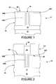
- FIG. 1is a cross-sectional view of a semiconductor device showing a conductive layer overlying a dielectric layer in which a via opening is formed, and on which a silver layer has been deposited;
- FIG. 2is a cross-sectional view similar to that shown in FIG. 1 but showing a pattered photoresist layer over the structure of FIG. 1 so as to define a trench opening communicating with the via opening, and further showing copper deposited by electroplating in such opening;
- FIG. 3is a cross-sectional view similar to that shown in FIG. 2 but showing the photoresist removed and an additional layer of silver deposited over the resulting structure;
- FIG. 4is a cross-sectional view similar to that shown in FIG. 3, illustrating the anneal step of the present invention
- FIG. 5is a cross-sectional view similar to that shown in FIG. 4 but showing removal of portions of the silver layers and addition of another dielectric layer;
- FIG. 6is a cross-sectional view of a second embodiment of the invention, showing a dielectric layer having a trench/via opening which communicates with a metal layer, and showing a seed layer containing palladium applied to the dielectric within the opening;
- FIG. 7is a cross-sectional view similar to that shown in FIG. 6 and showing a layer of silver applied over the resulting structure, and copper deposited by electroplating in the opening;
- FIG. 8is a cross-sectional view similar to that shown in FIG. 7 showing a seed layer containing palladium and an additional layer of silver on the exposed metal shown in FIG. 7 .
- FIG. 1Shown in FIG. 1 is a semiconductor structure 10 having a low k dielectric substrate 12 on which a conductive layer 14 , typically metal such as copper (Cu), is disposed.
- a low k dielectric layer 16is provided over the metal layer 14 , and through appropriate masking and etching of the dielectric layer 16 , a via opening 18 of high aspect ratio, in accordance with current practice, is formed in the dielectric layer 16 . This opening 18 communicates with the metal layer 14 under the dielectric layer 16 .
- a layer of silver (Ag) 20is deposited over the resulting structure, having a portion 20 A within the opening 18 in the dielectric layer 16 , i.e., on the sidewalls and in contact with the metal layer 14 , and on the top surface 22 of the dielectric layer 16 .
- the provision of this silver layer 20may be undertaken by in a variety of ways, for example, by physical vapor deposition (PVD), chemical vapor deposition (CVD), atomic layer deposition, or electroless deposition.
- PVDphysical vapor deposition
- CVDchemical vapor deposition
- atomic layer depositionatomic layer deposition
- electroless depositionAn example of electroless deposition of the silver layer 20 will now be described:
- the silver layer 20is continuous and highly conformal to the dielectric 16 , and has a thickness of for example 100-300 angstroms.
- annealing of the silver 20is undertaken at 100-200° C. to reduce the resistance thereof from approximately 3 ⁇ ohms.cm. to approximately 1.6 ⁇ ohms.cm.
- a layer of photoresist 24is provided over the resulting structure, and standard lithographic techniques are used to form a trench opening 26 in the resist 24 which communicates with the via opening 18 in the dielectric layer 16 . Thereafter, a selective copper electroplating process is undertaken to deposit copper 28 in the trench/via openings, to form a copper interconnect structure 28 . After removal of the resist layer 24 , which leaves a portion of the copper interconnect structure 28 extending above the surface 22 of the dielectric layer 16 (FIG.
- a layer of silver 30is electrolessly deposited over the resulting structure in the manner described above, having a portion 30 A over the exposed portion of the copper interconnect structure 28 , and portions 30 B, 30 C overlying the portions 20 B, 20 C of the silver layer 20 on the dielectric layer 16 .
- the copper interconnect structure 28is encapsulated or encased in silver.
- An anneal stepis then undertaken, for example at a temperature of 250-450° C., so that a copper-silver alloy 32 is formed at the interface or boundary of the copper and silver.
- Thecauses the copper interconnect structure 28 to be encapsulated by copper-silver alloy 32 .
- an additional dielectric layer 34is deposited over the resulting structure, and standard lithographic and etching techniques are used to form a via opening 36 in the dielectric layer 34 . It will readily be seen that further steps will be undertaken in the formation of a complete semiconductor structure.
- the silver layers 20 , 30have high conformality, readily lending themselves to use in trench/via openings which have a high aspect ratio. Furthermore, the silver layer 20 serves as a seed layer for electroplating copper in very small geometries of trench/vias.
- the copper-silver alloy layer 32 encapsulating the copper interconnect 28increases electromigration resistance of the copper interconnect 28 by restriction of copper diffusion at the interface of the copper with other materials.
- the copper-silver alloy 32has a low resistance characteristic which does not increase the resistance of the copper interconnect 28 .
- FIGS. 6-8As shown therein, a dual damascene via/trench formation of a low k dielectric layer 50 is undertaken by standard photolithographic and etching techniques, so that a trench/via opening 52 is provided in the dielectric layer 50 communicating with a bottom metallization layer 54 of copper disposed on a low k dielectric substrate 56 .
- a seed layer 58 containing palladiumis formed on the surface of the dielectric 50 , in particular in the opening 52 , by immersion in for example an aqueous contact activation solution containing the following:
- the conditions for activating the seed layerare as follows:
- a seed layer 10-30 angstroms thick containing palladiumis formed, and then a silver layer 60 is deposited over the resulting structure (FIG. 6) by application of silver-electroless solution as described above. This results in formation of a silver layer 60 100-300 angstroms thick, which is continuous and highly conformal to the trench/via opening 52 .
- a bulk copper layer 62is deposited by copper electroplating in a standard solution.
- CMPchemical mechanical polishing
- another seed layer 64is formed to a thickness of 10-30 angstroms, using the same solution as described above, with low concentration of metal ions, only over the exposed metal surfaces of the copper interconnect structure 62 A.
- a layer of silver 66is electrolessly deposited, using a solution with low concentration of silver ions and formaldehyde (or glyoxalic acid) only on the exposed metal surfaces, as described above, the layer 64 acting as a seed layer for the deposition of the silver 66 .
- An anneal stepis undertaken similar to that described in the previous embodiment, so that a copper-silver alloy is formed which encapsulates the interconnect 62 A.
- the present methodsreadily lend themselves to sub-0. 1 micron metallization features with high aspect ratios, for example, 5:1 or greater. It will be noted that the present methods do not use metallic barrier layers against copper or silver diffusion which would increase resistivity of a copper interconnect with such small dimensions.
- the low k dielectricserves as a barrier against copper or silver diffusion i.e., for example, benzocyclobutene (BCB) type dielectric.
- a conformal dielectric barrierfor example silicon nitride, can be deposited on the dielectric prior to application of the silver layer, if this is considered desirable for protection of active devices from copper or silver diffusion.
- the methods disclosed aboveprovide for high conformity of a base layer in a copper electroplating process, so that such methods can readily be applied to formation of interconnects with a high aspect ratio.
- the low resistivity silver or copper-silver alloy at the copper/dielectric interfaceleads to high electromigration resistance and high conductivity of the copper metallization.
Landscapes
- Physics & Mathematics (AREA)
- Condensed Matter Physics & Semiconductors (AREA)
- General Physics & Mathematics (AREA)
- Engineering & Computer Science (AREA)
- Computer Hardware Design (AREA)
- Microelectronics & Electronic Packaging (AREA)
- Power Engineering (AREA)
- Internal Circuitry In Semiconductor Integrated Circuit Devices (AREA)
Abstract
Description
| AgNO3 | 10-70 | mg/l |
| Ethylenediamine | 0.1-0.3 | g/l |
| (or Ethylenediamine tetraacetic acid) | ||
| KOH (or tetramethyl ammonium hydroxide) | 40-70 | mg/l |
| Formaldehyde HCOH (or glyoxalic acid) | 0.2-0.5 | ml/l |
| Additives (surfactants) | 0.01-0.05 | ml/l; |
| SnCl2 | 1-30 | grams/liter | ||
| PdCl2 | 0.02-5 | ml./liter | ||
| HCl | 0.5-7 | ml./liter | ||
| HF (49)% | 1-40 | ml./liter | ||
| Temperature | 18-25° C. | ||
| pH | 1-3 | ||
| Time | 3-60 seconds | ||
Claims (7)
Priority Applications (1)
| Application Number | Priority Date | Filing Date | Title |
|---|---|---|---|
| US09/592,164US6291082B1 (en) | 2000-06-13 | 2000-06-13 | Method of electroless ag layer formation for cu interconnects |
Applications Claiming Priority (1)
| Application Number | Priority Date | Filing Date | Title |
|---|---|---|---|
| US09/592,164US6291082B1 (en) | 2000-06-13 | 2000-06-13 | Method of electroless ag layer formation for cu interconnects |
Publications (1)
| Publication Number | Publication Date |
|---|---|
| US6291082B1true US6291082B1 (en) | 2001-09-18 |
Family
ID=24369571
Family Applications (1)
| Application Number | Title | Priority Date | Filing Date |
|---|---|---|---|
| US09/592,164Expired - LifetimeUS6291082B1 (en) | 2000-06-13 | 2000-06-13 | Method of electroless ag layer formation for cu interconnects |
Country Status (1)
| Country | Link |
|---|---|
| US (1) | US6291082B1 (en) |
Cited By (27)
| Publication number | Priority date | Publication date | Assignee | Title |
|---|---|---|---|---|
| US6391775B1 (en)* | 1997-09-18 | 2002-05-21 | Ebara Corporation | Method of forming embedded copper interconnections and embedded copper interconnection structure |
| US6472310B1 (en) | 2002-04-08 | 2002-10-29 | Advanced Micro Devices, Inc. | Tin palladium activation with maximized nuclei density and uniformity on barrier material in interconnect structure |
| US6537912B1 (en) | 2000-08-25 | 2003-03-25 | Micron Technology Inc. | Method of forming an encapsulated conductive pillar |
| US6538327B1 (en)* | 2000-07-28 | 2003-03-25 | Advanced Micro Devices, Inc. | Method of copper interconnect formation using atomic layer copper deposition and a device thereby formed |
| US20030075808A1 (en)* | 2001-08-13 | 2003-04-24 | Hiroaki Inoue | Semiconductor device, method for manufacturing the same, and plating solution |
| US20030171003A1 (en)* | 2002-03-07 | 2003-09-11 | Lg. Philips Lcd Co., Ltd. | Low resistivity copper conductor line, liquid crystal display device having the same and method for forming the same |
| US20030190426A1 (en)* | 2002-04-03 | 2003-10-09 | Deenesh Padhi | Electroless deposition method |
| US20040004289A1 (en)* | 2002-07-04 | 2004-01-08 | Kazuyoshi Ueno | Semiconductor device and manufacturing method thereof |
| US20040112753A1 (en)* | 2002-12-16 | 2004-06-17 | Susrut Kesari | Methods for polishing and/or cleaning copper interconnects and/or film and compositons therefor |
| US20040112756A1 (en)* | 2002-12-16 | 2004-06-17 | 3M Innovative Properties Company | Plating solutions for electrochemical or chemical deposition of copper interconnects and methods therefor |
| US20040112759A1 (en)* | 2002-12-16 | 2004-06-17 | Zazzera Lawrence A. | Methods for polishing and/or cleaning copper interconnects and/or film and compositions therefor |
| US20040235298A1 (en)* | 2001-11-06 | 2004-11-25 | Hiroaki Inoue | Plating solution, semiconductor device and method for manufacturing the same |
| US20050090098A1 (en)* | 2003-10-27 | 2005-04-28 | Dubin Valery M. | Method for making a semiconductor device having increased conductive material reliability |
| US20050124158A1 (en)* | 2003-10-15 | 2005-06-09 | Lopatin Sergey D. | Silver under-layers for electroless cobalt alloys |
| US20050136193A1 (en)* | 2003-10-17 | 2005-06-23 | Applied Materials, Inc. | Selective self-initiating electroless capping of copper with cobalt-containing alloys |
| US20050136185A1 (en)* | 2002-10-30 | 2005-06-23 | Sivakami Ramanathan | Post rinse to improve selective deposition of electroless cobalt on copper for ULSI application |
| US20050140013A1 (en)* | 2002-04-26 | 2005-06-30 | Kazuyoshi Ueno | Semiconductor device and manufacturing process therefor as well as plating solution |
| US20050164497A1 (en)* | 2004-01-26 | 2005-07-28 | Sergey Lopatin | Pretreatment for electroless deposition |
| US7205233B2 (en) | 2003-11-07 | 2007-04-17 | Applied Materials, Inc. | Method for forming CoWRe alloys by electroless deposition |
| US7514353B2 (en) | 2005-03-18 | 2009-04-07 | Applied Materials, Inc. | Contact metallization scheme using a barrier layer over a silicide layer |
| US7651934B2 (en) | 2005-03-18 | 2010-01-26 | Applied Materials, Inc. | Process for electroless copper deposition |
| US7659203B2 (en) | 2005-03-18 | 2010-02-09 | Applied Materials, Inc. | Electroless deposition process on a silicon contact |
| US20110298135A1 (en)* | 2007-10-24 | 2011-12-08 | Charan Gurumurthy | Integrated circuit and process for fabricating thereof |
| US8829482B1 (en)* | 2010-09-23 | 2014-09-09 | Adesto Technologies Corporation | Variable impedance memory device structure and method of manufacture including programmable impedance memory cells and methods of forming the same |
| US20140252628A1 (en)* | 2013-03-08 | 2014-09-11 | Taiwan Semiconductor Manufacturing Company, Ltd. | Interconnect structure and methods of making same |
| US20190029122A1 (en)* | 2017-07-19 | 2019-01-24 | Anaren, Inc. | Encapsulation of circuit trace |
| US10283372B2 (en) | 2017-09-15 | 2019-05-07 | Globalfoundries Inc. | Interconnects formed by a metal replacement process |
Citations (6)
| Publication number | Priority date | Publication date | Assignee | Title |
|---|---|---|---|---|
| US5824599A (en)* | 1996-01-16 | 1998-10-20 | Cornell Research Foundation, Inc. | Protected encapsulation of catalytic layer for electroless copper interconnect |
| US5969422A (en)* | 1997-05-15 | 1999-10-19 | Advanced Micro Devices, Inc. | Plated copper interconnect structure |
| US6022808A (en)* | 1998-03-16 | 2000-02-08 | Advanced Micro Devices, Inc. | Copper interconnect methodology for enhanced electromigration resistance |
| US6100194A (en)* | 1998-06-22 | 2000-08-08 | Stmicroelectronics, Inc. | Silver metallization by damascene method |
| US6136707A (en)* | 1999-10-02 | 2000-10-24 | Cohen; Uri | Seed layers for interconnects and methods for fabricating such seed layers |
| US6197688B1 (en)* | 1998-02-12 | 2001-03-06 | Motorola Inc. | Interconnect structure in a semiconductor device and method of formation |
- 2000
- 2000-06-13USUS09/592,164patent/US6291082B1/ennot_activeExpired - Lifetime
Patent Citations (6)
| Publication number | Priority date | Publication date | Assignee | Title |
|---|---|---|---|---|
| US5824599A (en)* | 1996-01-16 | 1998-10-20 | Cornell Research Foundation, Inc. | Protected encapsulation of catalytic layer for electroless copper interconnect |
| US5969422A (en)* | 1997-05-15 | 1999-10-19 | Advanced Micro Devices, Inc. | Plated copper interconnect structure |
| US6197688B1 (en)* | 1998-02-12 | 2001-03-06 | Motorola Inc. | Interconnect structure in a semiconductor device and method of formation |
| US6022808A (en)* | 1998-03-16 | 2000-02-08 | Advanced Micro Devices, Inc. | Copper interconnect methodology for enhanced electromigration resistance |
| US6100194A (en)* | 1998-06-22 | 2000-08-08 | Stmicroelectronics, Inc. | Silver metallization by damascene method |
| US6136707A (en)* | 1999-10-02 | 2000-10-24 | Cohen; Uri | Seed layers for interconnects and methods for fabricating such seed layers |
Non-Patent Citations (1)
| Title |
|---|
| Silver Metallization for Advanced Interconnects, Manepalli et al., IEEE Transactionson Advanced Packaging, vol. 22, No. 1, Feb. 1999. |
Cited By (58)
| Publication number | Priority date | Publication date | Assignee | Title |
|---|---|---|---|---|
| US6391775B1 (en)* | 1997-09-18 | 2002-05-21 | Ebara Corporation | Method of forming embedded copper interconnections and embedded copper interconnection structure |
| US6787467B2 (en)* | 1997-09-18 | 2004-09-07 | Ebara Corporation | Method of forming embedded copper interconnections and embedded copper interconnection structure |
| US6538327B1 (en)* | 2000-07-28 | 2003-03-25 | Advanced Micro Devices, Inc. | Method of copper interconnect formation using atomic layer copper deposition and a device thereby formed |
| US6566701B2 (en)* | 2000-08-25 | 2003-05-20 | Micron Technology, Inc. | Encapsulated conductive pillar |
| US6537912B1 (en) | 2000-08-25 | 2003-03-25 | Micron Technology Inc. | Method of forming an encapsulated conductive pillar |
| US20080011228A1 (en)* | 2001-08-13 | 2008-01-17 | Hiroaki Inoue | Semiconductor device, method for manufacturing the same, and plating solution |
| US7060618B2 (en)* | 2001-08-13 | 2006-06-13 | Ebara Corporation | Semiconductor device, method for manufacturing the same, and plating solution |
| US7279408B2 (en) | 2001-08-13 | 2007-10-09 | Ebara Corporation | Semiconductor device, method for manufacturing the same, and plating solution |
| US20030075808A1 (en)* | 2001-08-13 | 2003-04-24 | Hiroaki Inoue | Semiconductor device, method for manufacturing the same, and plating solution |
| US20060040487A1 (en)* | 2001-08-13 | 2006-02-23 | Hiroaki Inoue | Semiconductor device, method for manufacturing the same, and plating solution |
| US7344986B2 (en)* | 2001-11-06 | 2008-03-18 | Ebara Corporation | Plating solution, semiconductor device and method for manufacturing the same |
| US20040235298A1 (en)* | 2001-11-06 | 2004-11-25 | Hiroaki Inoue | Plating solution, semiconductor device and method for manufacturing the same |
| US20030171003A1 (en)* | 2002-03-07 | 2003-09-11 | Lg. Philips Lcd Co., Ltd. | Low resistivity copper conductor line, liquid crystal display device having the same and method for forming the same |
| US6858479B2 (en)* | 2002-03-07 | 2005-02-22 | Lg.Philips Lcd Co., Ltd. | Low resistivity copper conductor line, liquid crystal display device having the same and method for forming the same |
| US20030190426A1 (en)* | 2002-04-03 | 2003-10-09 | Deenesh Padhi | Electroless deposition method |
| US6472310B1 (en) | 2002-04-08 | 2002-10-29 | Advanced Micro Devices, Inc. | Tin palladium activation with maximized nuclei density and uniformity on barrier material in interconnect structure |
| CN100459066C (en)* | 2002-04-26 | 2009-02-04 | 恩益禧电子股份有限公司 | Semiconductor device and manufacturing process therefor as well as plating solution |
| CN100456438C (en)* | 2002-04-26 | 2009-01-28 | 恩益禧电子股份有限公司 | Semiconductor device and manufacturing method and plating solution |
| US7821135B2 (en) | 2002-04-26 | 2010-10-26 | Nec Electronics Corporation | Semiconductor device with improved stress migration resistance and manufacturing process therefor |
| US7259095B2 (en)* | 2002-04-26 | 2007-08-21 | Nec Electronics Corporation | Semiconductor device and manufacturing process therefor as well as plating solution |
| US20050140013A1 (en)* | 2002-04-26 | 2005-06-30 | Kazuyoshi Ueno | Semiconductor device and manufacturing process therefor as well as plating solution |
| DE10318921B4 (en)* | 2002-04-26 | 2015-02-19 | Renesas Electronics Corporation | Manufacturing method for a semiconductor device |
| US20050196959A1 (en)* | 2002-04-26 | 2005-09-08 | Kazuykoshi Ueno | Semiconductor device and manufacturing process therefor as well as plating solution |
| US7332813B2 (en)* | 2002-07-04 | 2008-02-19 | Nec Electronics Corporation | Semiconductor device |
| US20040004289A1 (en)* | 2002-07-04 | 2004-01-08 | Kazuyoshi Ueno | Semiconductor device and manufacturing method thereof |
| US20050136185A1 (en)* | 2002-10-30 | 2005-06-23 | Sivakami Ramanathan | Post rinse to improve selective deposition of electroless cobalt on copper for ULSI application |
| US7147767B2 (en) | 2002-12-16 | 2006-12-12 | 3M Innovative Properties Company | Plating solutions for electrochemical or chemical deposition of copper interconnects and methods therefor |
| US6884338B2 (en) | 2002-12-16 | 2005-04-26 | 3M Innovative Properties Company | Methods for polishing and/or cleaning copper interconnects and/or film and compositions therefor |
| US20040112753A1 (en)* | 2002-12-16 | 2004-06-17 | Susrut Kesari | Methods for polishing and/or cleaning copper interconnects and/or film and compositons therefor |
| US20040112759A1 (en)* | 2002-12-16 | 2004-06-17 | Zazzera Lawrence A. | Methods for polishing and/or cleaning copper interconnects and/or film and compositions therefor |
| US20040112756A1 (en)* | 2002-12-16 | 2004-06-17 | 3M Innovative Properties Company | Plating solutions for electrochemical or chemical deposition of copper interconnects and methods therefor |
| US6858124B2 (en) | 2002-12-16 | 2005-02-22 | 3M Innovative Properties Company | Methods for polishing and/or cleaning copper interconnects and/or film and compositions therefor |
| US7064065B2 (en) | 2003-10-15 | 2006-06-20 | Applied Materials, Inc. | Silver under-layers for electroless cobalt alloys |
| US20050124158A1 (en)* | 2003-10-15 | 2005-06-09 | Lopatin Sergey D. | Silver under-layers for electroless cobalt alloys |
| US20050136193A1 (en)* | 2003-10-17 | 2005-06-23 | Applied Materials, Inc. | Selective self-initiating electroless capping of copper with cobalt-containing alloys |
| US7229922B2 (en)* | 2003-10-27 | 2007-06-12 | Intel Corporation | Method for making a semiconductor device having increased conductive material reliability |
| US20050090098A1 (en)* | 2003-10-27 | 2005-04-28 | Dubin Valery M. | Method for making a semiconductor device having increased conductive material reliability |
| WO2005045923A1 (en)* | 2003-10-27 | 2005-05-19 | Intel Corporation | A method for making a semiconductor device having increased conductive material reliability |
| US7372165B2 (en) | 2003-10-27 | 2008-05-13 | Intel Corporation | Method for making a semiconductor device having increased conductive material reliability |
| US20050161828A1 (en)* | 2003-10-27 | 2005-07-28 | Dubin Valery M. | Method for making a semiconductor device having increased conductive material reliability |
| US7205233B2 (en) | 2003-11-07 | 2007-04-17 | Applied Materials, Inc. | Method for forming CoWRe alloys by electroless deposition |
| US7256111B2 (en)* | 2004-01-26 | 2007-08-14 | Applied Materials, Inc. | Pretreatment for electroless deposition |
| US20050164497A1 (en)* | 2004-01-26 | 2005-07-28 | Sergey Lopatin | Pretreatment for electroless deposition |
| US7514353B2 (en) | 2005-03-18 | 2009-04-07 | Applied Materials, Inc. | Contact metallization scheme using a barrier layer over a silicide layer |
| US7659203B2 (en) | 2005-03-18 | 2010-02-09 | Applied Materials, Inc. | Electroless deposition process on a silicon contact |
| US8308858B2 (en) | 2005-03-18 | 2012-11-13 | Applied Materials, Inc. | Electroless deposition process on a silicon contact |
| US7651934B2 (en) | 2005-03-18 | 2010-01-26 | Applied Materials, Inc. | Process for electroless copper deposition |
| US20110298135A1 (en)* | 2007-10-24 | 2011-12-08 | Charan Gurumurthy | Integrated circuit and process for fabricating thereof |
| US9941158B2 (en)* | 2007-10-24 | 2018-04-10 | Intel Corporation | Integrated circuit and process for fabricating thereof |
| US8829482B1 (en)* | 2010-09-23 | 2014-09-09 | Adesto Technologies Corporation | Variable impedance memory device structure and method of manufacture including programmable impedance memory cells and methods of forming the same |
| US9136166B2 (en)* | 2013-03-08 | 2015-09-15 | Taiwan Semiconductor Manufacturing Company, Ltd. | Interconnect structure and methods of making same |
| US20150340283A1 (en)* | 2013-03-08 | 2015-11-26 | Taiwan Semiconductor Manufacturing Company, Ltd. | Interconnect structure and methods of making same |
| US9576851B2 (en)* | 2013-03-08 | 2017-02-21 | Taiwan Semiconductor Manufacturing Company, Ltd. | Interconnect structure and methods of making same |
| US20170154814A1 (en)* | 2013-03-08 | 2017-06-01 | Taiwan Semiconductor Manufacturing Company, Ltd. | Interconnect structure and methods of making same |
| US20140252628A1 (en)* | 2013-03-08 | 2014-09-11 | Taiwan Semiconductor Manufacturing Company, Ltd. | Interconnect structure and methods of making same |
| US10186455B2 (en)* | 2013-03-08 | 2019-01-22 | Taiwan Semiconductor Manufacturing Company, Ltd. | Interconnect structure and methods of making same |
| US20190029122A1 (en)* | 2017-07-19 | 2019-01-24 | Anaren, Inc. | Encapsulation of circuit trace |
| US10283372B2 (en) | 2017-09-15 | 2019-05-07 | Globalfoundries Inc. | Interconnects formed by a metal replacement process |
Similar Documents
| Publication | Publication Date | Title |
|---|---|---|
| US6291082B1 (en) | Method of electroless ag layer formation for cu interconnects | |
| US5969422A (en) | Plated copper interconnect structure | |
| US6249055B1 (en) | Self-encapsulated copper metallization | |
| US6316359B1 (en) | Interconnect structure in a semiconductor device and method of formation | |
| US6022808A (en) | Copper interconnect methodology for enhanced electromigration resistance | |
| US6242349B1 (en) | Method of forming copper/copper alloy interconnection with reduced electromigration | |
| US5695810A (en) | Use of cobalt tungsten phosphide as a barrier material for copper metallization | |
| US5968333A (en) | Method of electroplating a copper or copper alloy interconnect | |
| US6756301B2 (en) | Method of forming a metal seed layer for subsequent plating | |
| US6972254B1 (en) | Manufacturing a conformal atomic liner layer in an integrated circuit interconnect | |
| US6509267B1 (en) | Method of forming low resistance barrier on low k interconnect with electrolessly plated copper seed layer | |
| US7008872B2 (en) | Use of conductive electrolessly deposited etch stop layers, liner layers and via plugs in interconnect structures | |
| EP1346408B1 (en) | Method of electroless introduction of interconnect structures | |
| US6455425B1 (en) | Selective deposition process for passivating top interface of damascene-type Cu interconnect lines | |
| US5891513A (en) | Electroless CU deposition on a barrier layer by CU contact displacement for ULSI applications | |
| US7304388B2 (en) | Method and apparatus for an improved air gap interconnect structure | |
| US6444567B1 (en) | Process for alloying damascene-type Cu interconnect lines | |
| US7879720B2 (en) | Methods of forming electrical interconnects using electroless plating techniques that inhibit void formation | |
| US6998342B2 (en) | Electronic device manufacturing method | |
| CN100517621C (en) | Interconnection structure with cladding layer and its manufacturing method | |
| US8053894B2 (en) | Surface treatment of metal interconnect lines | |
| US6656834B1 (en) | Method of selectively alloying interconnect regions by deposition process | |
| TW200301524A (en) | Method for improving electromigration performance of metallization features through multiple depositions of binary alloys | |
| US6875260B2 (en) | Copper activator solution and method for semiconductor seed layer enhancement | |
| US6555171B1 (en) | Cu/Sn/Pd activation of a barrier layer for electroless CU deposition |
Legal Events
| Date | Code | Title | Description |
|---|---|---|---|
| AS | Assignment | Owner name:ADVANCED MICRO DEVICES, INC., CALIFORNIA Free format text:ASSIGNMENT OF ASSIGNORS INTEREST;ASSIGNOR:LOPATIN, SERGEY;REEL/FRAME:010897/0819 Effective date:20000608 | |
| STCF | Information on status: patent grant | Free format text:PATENTED CASE | |
| FPAY | Fee payment | Year of fee payment:4 | |
| FPAY | Fee payment | Year of fee payment:8 | |
| AS | Assignment | Owner name:GLOBALFOUNDRIES INC., CAYMAN ISLANDS Free format text:AFFIRMATION OF PATENT ASSIGNMENT;ASSIGNOR:ADVANCED MICRO DEVICES, INC.;REEL/FRAME:023119/0083 Effective date:20090630 | |
| FPAY | Fee payment | Year of fee payment:12 | |
| AS | Assignment | Owner name:WILMINGTON TRUST, NATIONAL ASSOCIATION, DELAWARE Free format text:SECURITY AGREEMENT;ASSIGNOR:GLOBALFOUNDRIES INC.;REEL/FRAME:049490/0001 Effective date:20181127 | |
| AS | Assignment | Owner name:GLOBALFOUNDRIES INC., CAYMAN ISLANDS Free format text:RELEASE BY SECURED PARTY;ASSIGNOR:WILMINGTON TRUST, NATIONAL ASSOCIATION;REEL/FRAME:054636/0001 Effective date:20201117 | |
| AS | Assignment | Owner name:GLOBALFOUNDRIES U.S. INC., NEW YORK Free format text:RELEASE BY SECURED PARTY;ASSIGNOR:WILMINGTON TRUST, NATIONAL ASSOCIATION;REEL/FRAME:056987/0001 Effective date:20201117 |