US6288597B1 - Temperature sensing circuit for voltage drive type semiconductor device and temperature sensing method therefore, and drive-device and voltage drive type semiconductor device using the same - Google Patents
Temperature sensing circuit for voltage drive type semiconductor device and temperature sensing method therefore, and drive-device and voltage drive type semiconductor device using the sameDownload PDFInfo
- Publication number
- US6288597B1 US6288597B1US09/416,650US41665099AUS6288597B1US 6288597 B1US6288597 B1US 6288597B1US 41665099 AUS41665099 AUS 41665099AUS 6288597 B1US6288597 B1US 6288597B1
- Authority
- US
- United States
- Prior art keywords
- voltage
- resistor
- semiconductor element
- terminal
- semiconductor
- Prior art date
- Legal status (The legal status is an assumption and is not a legal conclusion. Google has not performed a legal analysis and makes no representation as to the accuracy of the status listed.)
- Expired - Lifetime
Links
- 239000004065semiconductorSubstances0.000titleclaimsabstractdescription104
- 238000000034methodMethods0.000titleclaimsabstractdescription11
- 230000000694effectsEffects0.000claimsdescription9
- 230000003247decreasing effectEffects0.000description13
- 238000010586diagramMethods0.000description7
- 239000002131composite materialSubstances0.000description5
- 238000001816coolingMethods0.000description5
- 239000002184metalSubstances0.000description4
- 230000005856abnormalityEffects0.000description3
- 239000012212insulatorSubstances0.000description2
- WABPQHHGFIMREM-UHFFFAOYSA-Nlead(0)Chemical compound[Pb]WABPQHHGFIMREM-UHFFFAOYSA-N0.000description1
- 230000000704physical effectEffects0.000description1
- 230000001681protective effectEffects0.000description1
- 230000009993protective functionEffects0.000description1
- 239000011347resinSubstances0.000description1
- 229920005989resinPolymers0.000description1
Images


Classifications
- H—ELECTRICITY
- H03—ELECTRONIC CIRCUITRY
- H03K—PULSE TECHNIQUE
- H03K17/00—Electronic switching or gating, i.e. not by contact-making and –breaking
- H03K17/08—Modifications for protecting switching circuit against overcurrent or overvoltage
- H03K17/082—Modifications for protecting switching circuit against overcurrent or overvoltage by feedback from the output to the control circuit
- H03K17/0828—Modifications for protecting switching circuit against overcurrent or overvoltage by feedback from the output to the control circuit in composite switches
- H—ELECTRICITY
- H01—ELECTRIC ELEMENTS
- H01L—SEMICONDUCTOR DEVICES NOT COVERED BY CLASS H10
- H01L2224/00—Indexing scheme for arrangements for connecting or disconnecting semiconductor or solid-state bodies and methods related thereto as covered by H01L24/00
- H01L2224/01—Means for bonding being attached to, or being formed on, the surface to be connected, e.g. chip-to-package, die-attach, "first-level" interconnects; Manufacturing methods related thereto
- H01L2224/42—Wire connectors; Manufacturing methods related thereto
- H01L2224/47—Structure, shape, material or disposition of the wire connectors after the connecting process
- H01L2224/49—Structure, shape, material or disposition of the wire connectors after the connecting process of a plurality of wire connectors
- H01L2224/491—Disposition
- H01L2224/4911—Disposition the connectors being bonded to at least one common bonding area, e.g. daisy chain
- H01L2224/49111—Disposition the connectors being bonded to at least one common bonding area, e.g. daisy chain the connectors connecting two common bonding areas, e.g. Litz or braid wires
- H—ELECTRICITY
- H03—ELECTRONIC CIRCUITRY
- H03K—PULSE TECHNIQUE
- H03K17/00—Electronic switching or gating, i.e. not by contact-making and –breaking
- H03K17/08—Modifications for protecting switching circuit against overcurrent or overvoltage
- H03K2017/0806—Modifications for protecting switching circuit against overcurrent or overvoltage against excessive temperature
Definitions
- the present inventionrelates to a temperature sensing circuit and a temperature sensing method for a voltage drive type semiconductor device.
- IGBTInsulated Gate Bipolar Transistor
- temperature sensing using a temperature sensing circuitis employed for detecting a temperature rise of the IGBT module in order to switch off the IGBT before it becomes damaged.
- IGBTInsulated Gate Bipolar Transistor
- the temperature rise of an IGBT moduleis detected by a temperature sensing circuit using a thermistor, and the signal produced by the temperature sensing circuit is transmitted to a control circuit to control the operation of the IGBT.
- the thermistoris attached on a cooling fin on which the IGBT module is mounted; and so, when the temperature of the cooling fin rises, the resistance of the thermistor is decreased and the terminal voltage thereof is also decreased.
- the temperature sensing circuitoperates to switch off the IGBT by making use of this characteristic.
- FIG. 6shows a temperature sensing circuit 31 using a thermistor 29 attached to a cooling fin, a control circuit 26 for controlling an IGBT module 9 a , and a gate drive circuit 12 .
- one end of the thermistor 29is connected in series with a resistor 30 and a voltage source, and the junction between the thermistor 29 and the resistor 30 is connected to an input terminal of a voltage comparing circuit 13 .
- the other end of the thermistor 29is connected to ground potential.
- a second input terminal of the voltage comparing circuit 13is connected to a constant voltage circuit 18 , and the output terminal thereof is connected to the control circuit 26 .
- the thermistor for temperature sensingis a part mounted on the cooling fin, a temperature change of the IGBT is sensed by the temperature of the cooling fin. Therefore, when an IGBT element 1 a generates heat due to an over-current or the like, there arises a problem in that the temperature transmitted to the thermistor differs depending on the position of the element which is generating heat. In this regard, the temperature sensing accuracy is decreased as the distance between the element and the thermistor increases.
- An object of the present inventionis to provide a highly reliable temperature sensing circuit and a highly reliable temperature sensing method by taking the above-mentioned problem into consideration.
- a temperature sensing circuit and a temperature sensing method in accordance with the present inventionare applied to a voltage drive type semiconductor device comprising a semiconductor element for controlling current flowing between a pair of main electrodes in response to a voltage applied to an insulated gate electrode of the semiconductor device; a gate terminal electrically connected to the insulated gate electrode; another terminal electrically connected to one main electrode among the pair of main electrodes.
- the semiconductor elementthere are various kinds of semiconductor elements having an insulated gate electrode, such as an MOSFET and so on, in addition to an IGBT.
- the voltage drive type semiconductor devicethere are, for example, a power semiconductor module, a resin seal type semiconductor device and so on.
- a resistor having a positive temperature coefficientis connected between the gate terminal and the insulated gate electrode of a voltage drive type semiconductor device. Further, the temperature sensing circuit comprises a means for receiving a voltage, representing a voltage drop across the resistor disposed in a circuit portion between the gate terminal and said other terminal, and for sensing the temperature of the voltage drive type semiconductor device based on the received voltage.
- the temperature sensing circuit in accordance with the present inventionmakes use of the fact that, when a resistor having a positive temperature coefficient is connected between the gate terminal and the insulated gate electrode of a semiconductor device, a voltage representing a voltage drop across the resistor disposed in a circuit portion between the gate terminal and said other terminal is changed by the temperature of the voltage drive type semiconductor device. Therefore, the sensing response to a temperature change in the voltage drive type semiconductor device becomes fast. Accordingly, by sensing the temperature based on the received voltage, a temperature sensing circuit having a high reliability can be obtained.
- a resistor having a positive temperature coefficientis connected between the gate terminal and the insulated gate electrode of the semiconductor element; and a temperature is sensed based on a voltage representing a voltage drop across the resistor disposed in a circuit portion between the gate terminal and said other terminal during a mirror effect condition which is generated when the semiconductor element turns off.
- the temperature sensing method in accordance with the present inventionmakes use of the fact that, when a resistor having a positive temperature coefficient is connected between the gate terminal and the insulated gate electrode of the semiconductor device, a voltage including a voltage drop across the resistor disposed in a circuit portion between the gate terminal and said other terminal during a mirror effect condition which is generated when the semiconductor element turns off. Accordingly, similar to the temperature sensing circuit in accordance with the present invention, as described above, the sensing response becomes fast and a temperature sensing circuit having a high reliability can be obtained.
- the resistor connected between the gate terminal and the insulated gate electrode in the voltage drive type semiconductor deviceis contained in the voltage drive type semiconductor device.
- the resistorsince the resistor is placed in a position near the semiconductor element, which represents the heat generating source, the temperature sensing accuracy can be improved.
- the resistorit is possible to use a resistor which is contained in the voltage drive type semiconductor device primarily for a purpose other than temperature sensing, such as a gate resistor.
- a drive device for a voltage drive type semiconductor device in accordance with the present inventioncomprises a drive circuit connected to the gate terminal through another resistor and to said other terminal; and the temperature sensing circuit in accordance with the present invention as described above.
- the drive device for a temperature sensing circuit in accordance with the present inventionmakes use of the fact that, when a resistor having a positive temperature coefficient is connected between the gate terminal and the insulated gate electrode and another resistor is connected between the drive circuit and the gate terminal, a voltage corresponding to a voltage drop across the resistor disposed in a circuit portion between the gate terminal and said other terminal is changed by the temperature of the voltage drive type semiconductor device. Therefore, by controlling the drive device based on the output signal of the temperature sensing circuit, a highly accurate protective operation relative to the temperature can be performed.
- the voltage drive type semiconductor devicecomprises a plurality of semiconductor elements
- the voltage drive type semiconductor devicehaving the following structure is suitable for use of the temperature sensing circuit and the temperature sensing method described above to effect temperature protection thereof.
- the voltage drive type semiconductor devicecomprises a semiconductor element controlling current flowing between a pair of main electrodes in accordance with a voltage applied to an insulated gate electrode of the semiconductor device; a gate terminal electrically connected to the insulated gate electrode; another terminal electrically connected to one main electrode among the pair of main electrodes; a resistor circuit including a resistor having a positive temperature coefficient connected between the gate terminal and the insulated gate electrode; another semiconductor element having an insulated gate electrode and being connected to the semiconductor element in parallel, wherein the resistor circuit comprises a first resistor and a second resistor connected to each other in series, and a third resistor connected between a junction point of the first resistor and the second resistor and the insulated gate electrode of the other semiconductor element.
- FIGS. 1A and 1Bare a schematic circuit diagram and a plan view, respectively, of a first embodiment of the present invention.
- FIG. 2is a schematic circuit diagram of a second embodiment of the present invention.
- FIG. 3is a schematic circuit diagram of a third embodiment of the present invention.
- FIG. 4is a schematic circuit diagram of a fourth embodiment of the present invention.
- FIGS. 5A and 5Bare a schematic circuit diagram and a waveform diagram, respectively, for explaining the operation of each embodiment of the present invention.
- FIG. 6is a schematic circuit diagram showing an example of the prior art.
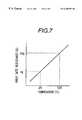
- FIG. 7is a graph which shows a relationship between temperature and inner gate resistance in the first embodiment.
- FIG. 1Ashows a first embodiment of the present invention.
- An inner gate resistor (rg) 10 ais connected between a gate electrode 8 a of an IGBT chip 1 a and a gate terminal 4 of an IGBT module 9 a
- an outer gate resistor (RG) 11is connected between the gate terminal 4 of the IGBT module 9 a and a gate drive circuit 12 .
- the gate terminal 4 of the IGBT module 9 ais connected to an input terminal (B) 15 of a voltage comparing circuit 13
- an auxiliary emitter terminal 5 of the IGBT module 9 ais connected to a ground terminal 16 of the voltage comprising circuit 13 and to the gate drive circuit 12 .
- a constant voltage circuit 18is connected to an input terminal (A) 14 of the voltage/comparing circuit 13 .
- FIG. 1Bis a view showing the inner structure of the IGBT module 9 a .
- An insulator plate 35is disposed on a heat radiating plate 36 , and metal plates 34 a , 34 b , 34 c are placed on the insulator plate 35 .
- a collector electrode portion of the IGBT chip 1 ais connected to the metal plate 34 b
- one end of the inner gate resistor 10 ais connected to the metal plate 34 c
- the other end of the inner gate resistor 10 ais connected to a gate electrode portion of the IGBT chip 1 a with a lead wire 33 .
- An electrode 3 for leading the emitter terminal to the outside of the module, an electrode 2 for leading the collector terminal to the outside of the module and an electrode 4 for leading the gate terminal to the outside of the moduleare connected to each of the metal plates 34 a , 34 b , 34 c , respectively.
- the change in the voltage drop across the inner gate resistor (rg) 10 ais detected as a voltage (VGE) 21 between the gate and the emitter, and this voltage (VGE) 21 is input to the input terminal (B) 15 of the voltage comparing circuit 13 .
- a constant voltage value from the constant voltage circuit 18is input to the other input terminal (A) 14 of the voltage comparing circuit 13 , and a voltage compared result of the voltage comparing circuit 13 is output from an output terminal 17 of the voltage comparing circuit 13 .
- FIG. 5 A and FIG. 5Bwill be used to explain the operation of the present embodiment.
- the timing for detecting the change in the voltage drop 19 generated across the inner gate resistor 10 a of the modulecorresponds to the time, ref erring to FIG. 5B, when the voltage (VGE) 21 between the gate and the emitter of the IGBT module 9 a is in a mirror effect occurring period A caused by the action of a feedback capacity existing between the collector electrode and the gate electrode of the IGBT chip 1 a at the time of turning-off of the IGBT chip 1 a .
- the gate voltage appearing between the gate and the emitter of the IGBT chip 1 a in the mirror effect occurring period A described aboveis a constant value, and the gate current value is a constant value.
- the voltage generated between the gate terminal 4 and the auxiliary emitter terminal 5 in the IGBT module 9 a shown in FIG. 5Ais the sum of the constant value of the gate voltage in the mirror effect occurring period A described above and the voltage value across the inner gate resistor 10 a of the module.
- the operation accompanied by a change in the temperature of the IGBT chip in this embodimentwill be described below.
- the temperature coefficients of the resistivity possessed by the resistors, such as the gate resistor mounted inside the module,are positive values.
- the resistance of the inner gate resistor (rg) 10 ais increased with the increase in temperature, and, accordingly, the voltage produced across the inner gate resistor (rg) 10 a is increased. Therefore, the constant voltage value generated between the gate terminal 4 and the auxiliary emitter terminal 5 in the period A of FIG. 5B is decreased, and the signal at the output terminal 17 of the temperature sensing circuit is inverted in polarity when the voltage value is decreased below the constant voltage value applied to the input terminal (A) 14 of the voltage comparing circuit 13 . In response to the signal at the output terminal 17 , a control circuit is operated, and, for example, the IGBT is turned off.
- the amount of change ( ⁇ VGE) in the gate voltage produced between the gate terminal 4 and the auxiliary emitter terminal 5 due to the temperature change of the inner gate resistor (rg) 10 a in the period Adepends on the ratio of the resistance value rg of the inner gate resistor (rg) 10 a to the resistance value RG of the outer gate resistor (RG) 11 .
- the temperature coefficient of the inner gate resistor (rg)be ⁇
- the voltage output from the gate drive circuit 12 in the period Abe VGN
- the gate threshold voltage possessed by the IGBT chip 1 a depending on the collector current 20 flowing in the IGBT module 9 abe VTH
- the temperature change of the inner gate resistor of the module in the period A shown in FIG. 5Bcan be considered as corresponding to the amount of change ⁇ VGE in the gate voltage produced between the gate terminal 4 and the auxiliary emitter terminal 5 . Therefore, the temperature of the IGBT module 9 a can be detected by using a calculator for calculating temperature based on the equation 1 in response to the gate voltage, instead of using the voltage comparing circuit.
- the output of the temperature sensing deviceinverts in polarity when the input voltage from gate terminal 14 is decreased below the constant voltage level at input terminal (A) 14 .
- the voltage of the input terminal (A) 14 of the voltage comparing circuit 13is assumed to be 3 V, and the voltage of the input terminal (B) 15 of the voltage comparing circuit 13 is changed from 5 V to 2.9 V in response to the temperature rise in the IGBT module 9 a from 25° C. to 125° C., the temperature sensing operation is performed because the voltage of the input terminal (B) 15 becomes lower than the applied voltage of the input terminal (A) 14 .
- FIG. 2shows a second embodiment of the present invention.
- This embodimentrepresents a case where a plurality of IGBTs are connected in parallel.
- An inner gate resistor (rg) 10 a and an inner gate resistor (rt) 22are connected in series between a gate electrode 8 a of an IGBT 1 a and a gate terminal 4 of an IGBT module 9 b , and an outer gate resistor (RG) 11 is connected between the gate terminal 4 of an IGBT module 9 b and a gate drive circuit 12 .
- RGouter gate resistor
- the gate terminal 4 of the IGBT module 9 bis connected to an input terminal (B) 15 of a voltage comparing circuit 13
- an auxiliary terminal 5 of the IGBT module 9 bis connected to a ground terminal 16 of the voltage comparing circuit 13 and to the gate drive circuit 12 .
- a constant voltage circuit 18is connected to an input terminal (A) 14 of the voltage comparing circuit 13 .
- a collector electrode 6 b of the IGBT 1 bis connected to a collector electrode 6 a of the IGBT 1 a
- an emitter electrode 7 b of the IGBT 1 bis connected to an emitter electrode 7 a of the IGBT 1 a
- an inner gate resistor (rg) 10 bis connected between the gate electrode 8 b of the IGBT 1 b and point 23 (that is, a junction point of the inner gate resistor 22 and the inner gate resistor 10 a ).
- the equivalent resistanceis increased to increase the voltage drop by connecting the inner gate resistor (rt) 22 in series to the combination of the inner gate resistors (rg) 10 a and 10 b.
- the timing of temperature sensingis performed in the period A when the voltage (VGE) 21 between the gate and the emitter of the IGBT module 9 b becomes a clamp voltage at the time of turning-off of the IGBT 1 a and the IGBT 1 b .
- a voltage dropis produced across the inner gate resistor by gate current 19 flowing at the time of turning-off of the IGBT 1 a and the IGBT 1 b to decrease the clamp voltage.
- the clamp voltage in the period of FIG. 5Bis further decreased, and the temperature sensing circuit is operated when the voltage value is decreased to a value below the constant voltage value applied to the input terminal (A) 14 of the voltage comparing circuit 13 .
- the amount of change ( ⁇ VGE) in the clamp voltage due to the temperature change of the inner gate resistor in the period Ais determined by the ratio of the composite resistance of the inner gate resistors (rg) 10 a , 10 b and the inner gate resistor (rt) 22 to the resistance of the outer gate resistor (RG) 11 .
- the temperature coefficient/of the composite inner gate resistorbe ⁇
- the composite inner gate resistancebe r
- the negative voltage applied to the gate terminal 4be VGN
- the clamp voltage depending on a collector current 20 flowing in the IGBT module 9 bbe VTH
- the temperature changecan be detected based on ⁇ VGE similarly to the first embodiment.
- FIG. 3shows a third embodiment of the present invention. This embodiment is another case where a plurality of IGBTs are connected in parallel.
- An inner gate resistor (rg) 10 a and an inner gate resistor (rt) 22are connected in series between a gate electrode 8 a of an IGBT 1 a and a gate terminal 4 of an IGBT module 9 c , and an outer gate resistor (RG) 11 is connected between the gate terminal 4 of the IGBT module 9 c and a gate drive circuit 12 .
- the gate terminal 4 of the IGBT module 9 bis connected to an input terminal (B) 15 of a voltage comparing circuit 13
- an auxiliary terminal 5 of the IGBT module 9 cis connected to a ground terminal 16 of the voltage comparing circuit 13 and to the gate drive circuit 12 .
- a constant voltage circuit 18is connected to an input terminal (A) 14 of the voltage comparing circuit 13 .
- a collector electrode 6 b of the IGBT 1 bis connected to a collector electrode 6 a of the IGBT 1 a
- an emitter electrode 7 b of the IGBT 1 bis connected to an emitter electrode 7 a of the IGBT 1 a
- an inner gate resistor (rg) 10 bis connected between the gate electrode 8 b of the IGBT 1 b and point (B) 23 (that is, a junction point of the inner gate resistor 22 and the inner gate resistor 10 a ).
- a temperature sensing terminal 24is provided and connected to the point 23 .
- the amount of change in the sensing levelis decreased because the equivalent resistance becomes small, and, accordingly, the voltage drop is decreased. Therefore, by connecting the inner gate resistor (rt) 22 in series with the inner gate resistors (rg) 10 a and 10 b , and, further, by connecting the temperature sensing terminal 24 to the point (B) 23 at the one end of the inner gate resistor (rt) 22 , the temperature detecting operation is performed by detecting the terminal voltage of the inner gate resistor (rt) 22 .
- the timing of temperature sensingis performed by detecting the voltage (VTG) between the temperature sensing terminal 24 and the gate terminal 4 in the period A when the voltage (VGE) 21 between the gate and the emitter of the IGBT module 9 c becomes a clamp voltage at the time of turning-off of the IGBT 1 a and the IGBT 1 b .
- the voltage (VTG) 25is generated in the inner gate resistor (rt) 22 by the gate current 19 flowing at the time of turning-off of the IGBT 1 a and the IGBT 1 b to decrease the clamp voltage.
- the present temperature sensing circuitis operated when the voltage value is increased with respect to the constant voltage value applied to the input terminal (A) 14 of the voltage comparing circuit 13 .
- Equation 3the amount of change ( ⁇ VTG) in the voltage produced in the inner gate resistor (rt) 22 by the temperature rise in the period A can be expressed by Equation 3.
- the temperature changecan be detected from the change ⁇ VTG in the gate voltage.
- FIG. 4shows a fourth embodiment of the present invention.
- the output of the voltage comparing circuit 13is connected to the control circuit 26
- the output of the control circuit 26is connected to the gate drive circuit 12 .
- the voltage comparing circuit 13regards this condition as the occurrence of an abnormality and outputs a signal indicating the abnormality to the control circuit 26 .
- the control circuit 26outputs an off operation instruction to the gate drive circuit 12 when receiving the signal indicating the abnormality.
- the gate drive circuit 12receives the off operation instruction, the gate drive circuit 12 operates to turn off the drive of the IGBT 1 a and the IGBT 1 b.
- examples of the present inventionhave been considered in which an IGBT is used as the switching element.
- a voltage drive type switching elementsuch as a power MOSET
- the circuit operationis the same as described above, and the same effect can be attained.
Landscapes
- Power Conversion In General (AREA)
- Measurement Of Current Or Voltage (AREA)
- Electronic Switches (AREA)
Abstract
Description
Claims (17)
Applications Claiming Priority (2)
| Application Number | Priority Date | Filing Date | Title |
|---|---|---|---|
| JP10-289060 | 1998-10-12 | ||
| JP28906098AJP3599575B2 (en) | 1998-10-12 | 1998-10-12 | Temperature detecting circuit of voltage-driven semiconductor device, driving device using the same, and voltage-driven semiconductor device |
Publications (1)
| Publication Number | Publication Date |
|---|---|
| US6288597B1true US6288597B1 (en) | 2001-09-11 |
Family
ID=17738312
Family Applications (1)
| Application Number | Title | Priority Date | Filing Date |
|---|---|---|---|
| US09/416,650Expired - LifetimeUS6288597B1 (en) | 1998-10-12 | 1999-10-12 | Temperature sensing circuit for voltage drive type semiconductor device and temperature sensing method therefore, and drive-device and voltage drive type semiconductor device using the same |
Country Status (4)
| Country | Link |
|---|---|
| US (1) | US6288597B1 (en) |
| EP (1) | EP0994565B1 (en) |
| JP (1) | JP3599575B2 (en) |
| DE (1) | DE69931120T2 (en) |
Cited By (12)
| Publication number | Priority date | Publication date | Assignee | Title |
|---|---|---|---|---|
| US20080001646A1 (en)* | 2006-06-30 | 2008-01-03 | Lui Sik K | Thermally stable semiconductor power device |
| US20090167414A1 (en)* | 2007-12-26 | 2009-07-02 | Infineon Technologies Ag | Temperature detection for a semiconductor component |
| US20120025873A1 (en)* | 2009-08-27 | 2012-02-02 | Fuji Electric Co., Ltd. | Semiconductor drive device |
| US20150371809A1 (en)* | 2014-06-06 | 2015-12-24 | Nuctech Company Limited | X-ray generator with adjustable collimation |
| US20160118891A1 (en)* | 2013-05-10 | 2016-04-28 | Hitachi, Ltd. | Apparatus for controlling insulating gate-type semiconductor element, and power conversion apparatus using apparatus for controlling insulating gate-type semiconductor element |
| US20160233040A1 (en)* | 2015-01-20 | 2016-08-11 | Electronics And Telecommunications Research Institute | Electrical switchgear for overcurrent protection using critical temperature device |
| US10069439B2 (en) | 2015-12-22 | 2018-09-04 | Renesas Electronics Corporation | Power conversion system, power module, and semiconductor device with diode coupling |
| US10658947B2 (en) | 2017-06-30 | 2020-05-19 | Renesas Electronics Corporation | Semiconductor device, power module, and control method of power conversion device |
| US20210011090A1 (en)* | 2019-07-11 | 2021-01-14 | Fuji Electric Co., Ltd. | Power semiconductor module and leakage current test method for the same |
| US10948359B2 (en) | 2018-10-30 | 2021-03-16 | Analog Devices International Unlimited Company | Techniques for junction temperature determination of power switches |
| US11388845B2 (en)* | 2017-03-31 | 2022-07-12 | Mitsubishi Electric Corporation | Multi-die temperature control device and method for controlling temperature of multi-die power module |
| US20220324635A1 (en)* | 2019-12-26 | 2022-10-13 | Canon Electron Tubes & Devices Co., Ltd. | X-ray tube packing device |
Families Citing this family (9)
| Publication number | Priority date | Publication date | Assignee | Title |
|---|---|---|---|---|
| DE102010029147B4 (en)* | 2010-05-20 | 2012-04-12 | Semikron Elektronik Gmbh & Co. Kg | Method for determining the temperature of a power semiconductor |
| CN103493372A (en)* | 2011-04-28 | 2014-01-01 | 皇家飞利浦有限公司 | Digitally controlled high speed high voltage gate driver circuit |
| JP6044215B2 (en)* | 2012-09-13 | 2016-12-14 | 富士電機株式会社 | Semiconductor device |
| JP6750360B2 (en)* | 2016-07-15 | 2020-09-02 | 富士電機株式会社 | Semiconductor device |
| WO2019058545A1 (en)* | 2017-09-25 | 2019-03-28 | 新電元工業株式会社 | Switching element control circuit and power module |
| JP6958499B2 (en)* | 2018-07-09 | 2021-11-02 | 三菱電機株式会社 | Semiconductor devices and power converters |
| KR102086519B1 (en)* | 2018-07-12 | 2020-03-09 | 엘지전자 주식회사 | Power transforming apparatus, compressor including the same and method for controlling the same |
| EP3955463A1 (en)* | 2020-08-10 | 2022-02-16 | Siemens Aktiengesellschaft | Parallel circuit of semiconductor switches |
| CN115206180B (en)* | 2022-07-25 | 2023-08-01 | 武汉华星光电技术有限公司 | Display panel and display device |
Citations (12)
| Publication number | Priority date | Publication date | Assignee | Title |
|---|---|---|---|---|
| US3898486A (en)* | 1972-10-25 | 1975-08-05 | Bosch Gmbh Robert | Stabilized threshold circuit for connection to sensing transducers and operation under varying voltage conditions |
| US4220877A (en)* | 1977-05-16 | 1980-09-02 | Rca Corporation | Temperature compensated switching circuit |
| US4914542A (en)* | 1988-12-27 | 1990-04-03 | Westinghouse Electric Corp. | Current limited remote power controller |
| US5045964A (en)* | 1990-04-30 | 1991-09-03 | Motorola, Inc. | Thermal clamp for an ignition coil driver |
| JPH06244413A (en) | 1993-02-22 | 1994-09-02 | Hitachi Ltd | Insulated gate semiconductor device |
| JPH0767383A (en) | 1993-08-24 | 1995-03-10 | Jidosha Denki Kogyo Co Ltd | Motor controller |
| US5444219A (en)* | 1990-09-24 | 1995-08-22 | U.S. Philips Corporation | Temperature sensing device and a temperature sensing circuit using such a device |
| US5631494A (en)* | 1993-09-17 | 1997-05-20 | Hitachi, Ltd. | Power semiconductor device with low on-state voltage |
| US5635823A (en)* | 1994-10-06 | 1997-06-03 | Kabushiki Kaisha Toshiba | Current detector circuit |
| US5723916A (en)* | 1996-05-17 | 1998-03-03 | Delco Electronics Corporation | Electrical load driving device including load current limiting circuitry |
| US5796290A (en) | 1995-10-26 | 1998-08-18 | Nec Corporation | Temperature detection method and circuit using MOSFET |
| US5886515A (en)* | 1997-02-19 | 1999-03-23 | U.S. Philips Corporation | Power semiconductor devices with a temperature sensor circuit |
Family Cites Families (2)
| Publication number | Priority date | Publication date | Assignee | Title |
|---|---|---|---|---|
| JPH0832361A (en)* | 1994-07-14 | 1996-02-02 | Toyota Autom Loom Works Ltd | Amplifier circuit provided with protection device |
| JP3265849B2 (en)* | 1994-09-16 | 2002-03-18 | 富士電機株式会社 | Self-extinguishing element with overheat protection device |
- 1998
- 1998-10-12JPJP28906098Apatent/JP3599575B2/ennot_activeExpired - Fee Related
- 1999
- 1999-09-24EPEP99118891Apatent/EP0994565B1/ennot_activeExpired - Lifetime
- 1999-09-24DEDE69931120Tpatent/DE69931120T2/ennot_activeExpired - Fee Related
- 1999-10-12USUS09/416,650patent/US6288597B1/ennot_activeExpired - Lifetime
Patent Citations (12)
| Publication number | Priority date | Publication date | Assignee | Title |
|---|---|---|---|---|
| US3898486A (en)* | 1972-10-25 | 1975-08-05 | Bosch Gmbh Robert | Stabilized threshold circuit for connection to sensing transducers and operation under varying voltage conditions |
| US4220877A (en)* | 1977-05-16 | 1980-09-02 | Rca Corporation | Temperature compensated switching circuit |
| US4914542A (en)* | 1988-12-27 | 1990-04-03 | Westinghouse Electric Corp. | Current limited remote power controller |
| US5045964A (en)* | 1990-04-30 | 1991-09-03 | Motorola, Inc. | Thermal clamp for an ignition coil driver |
| US5444219A (en)* | 1990-09-24 | 1995-08-22 | U.S. Philips Corporation | Temperature sensing device and a temperature sensing circuit using such a device |
| JPH06244413A (en) | 1993-02-22 | 1994-09-02 | Hitachi Ltd | Insulated gate semiconductor device |
| JPH0767383A (en) | 1993-08-24 | 1995-03-10 | Jidosha Denki Kogyo Co Ltd | Motor controller |
| US5631494A (en)* | 1993-09-17 | 1997-05-20 | Hitachi, Ltd. | Power semiconductor device with low on-state voltage |
| US5635823A (en)* | 1994-10-06 | 1997-06-03 | Kabushiki Kaisha Toshiba | Current detector circuit |
| US5796290A (en) | 1995-10-26 | 1998-08-18 | Nec Corporation | Temperature detection method and circuit using MOSFET |
| US5723916A (en)* | 1996-05-17 | 1998-03-03 | Delco Electronics Corporation | Electrical load driving device including load current limiting circuitry |
| US5886515A (en)* | 1997-02-19 | 1999-03-23 | U.S. Philips Corporation | Power semiconductor devices with a temperature sensor circuit |
Cited By (24)
| Publication number | Priority date | Publication date | Assignee | Title |
|---|---|---|---|---|
| CN101479940B (en)* | 2006-06-30 | 2012-02-29 | 万国半导体股份有限公司 | High power semiconductor components with good thermal stability |
| US7443225B2 (en)* | 2006-06-30 | 2008-10-28 | Alpha & Omega Semiconductor, Ltd. | Thermally stable semiconductor power device |
| WO2008005401A3 (en)* | 2006-06-30 | 2008-12-04 | Alpha & Omega Semiconductor | Thermally stable semiconductor power device |
| US20090128223A1 (en)* | 2006-06-30 | 2009-05-21 | Lui Sik K | Thermally stable semiconductor power device |
| US20080001646A1 (en)* | 2006-06-30 | 2008-01-03 | Lui Sik K | Thermally stable semiconductor power device |
| US7671662B2 (en)* | 2006-06-30 | 2010-03-02 | Alpha And Omega Semiconductor Incorporated | Thermally stable semiconductor power device |
| US7988354B2 (en)* | 2007-12-26 | 2011-08-02 | Infineon Technologies Ag | Temperature detection for a semiconductor component |
| US20090167414A1 (en)* | 2007-12-26 | 2009-07-02 | Infineon Technologies Ag | Temperature detection for a semiconductor component |
| US20120025873A1 (en)* | 2009-08-27 | 2012-02-02 | Fuji Electric Co., Ltd. | Semiconductor drive device |
| US8487668B2 (en)* | 2009-08-27 | 2013-07-16 | Fuji Electric Co., Ltd. | Semiconductor drive device |
| US10038380B2 (en) | 2013-05-10 | 2018-07-31 | Hitachi, Ltd. | Apparatus for controlling insulating gate-type semiconductor element, and power conversion apparatus using apparatus for controlling insulating gate-type semiconductor element |
| US20160118891A1 (en)* | 2013-05-10 | 2016-04-28 | Hitachi, Ltd. | Apparatus for controlling insulating gate-type semiconductor element, and power conversion apparatus using apparatus for controlling insulating gate-type semiconductor element |
| US9780660B2 (en)* | 2013-05-10 | 2017-10-03 | Hitachi, Ltd. | Apparatus for controlling insulating gate-type semiconductor element, and power conversion apparatus using apparatus for controlling insulating gate-type semiconductor element |
| US20150371809A1 (en)* | 2014-06-06 | 2015-12-24 | Nuctech Company Limited | X-ray generator with adjustable collimation |
| US9779908B2 (en)* | 2014-06-06 | 2017-10-03 | Nuctech Company Limited | X-ray generator with adjustable collimation |
| US20160233040A1 (en)* | 2015-01-20 | 2016-08-11 | Electronics And Telecommunications Research Institute | Electrical switchgear for overcurrent protection using critical temperature device |
| US10553381B2 (en)* | 2015-01-20 | 2020-02-04 | Electronics And Telecommunications Research Institute | Electrical switchgear for overcurrent protection using critical temperature device |
| US10069439B2 (en) | 2015-12-22 | 2018-09-04 | Renesas Electronics Corporation | Power conversion system, power module, and semiconductor device with diode coupling |
| US11388845B2 (en)* | 2017-03-31 | 2022-07-12 | Mitsubishi Electric Corporation | Multi-die temperature control device and method for controlling temperature of multi-die power module |
| US10658947B2 (en) | 2017-06-30 | 2020-05-19 | Renesas Electronics Corporation | Semiconductor device, power module, and control method of power conversion device |
| US10948359B2 (en) | 2018-10-30 | 2021-03-16 | Analog Devices International Unlimited Company | Techniques for junction temperature determination of power switches |
| US20210011090A1 (en)* | 2019-07-11 | 2021-01-14 | Fuji Electric Co., Ltd. | Power semiconductor module and leakage current test method for the same |
| US11513165B2 (en)* | 2019-07-11 | 2022-11-29 | Fuji Electric Co., Ltd. | Power semiconductor module and leakage current test method for the same |
| US20220324635A1 (en)* | 2019-12-26 | 2022-10-13 | Canon Electron Tubes & Devices Co., Ltd. | X-ray tube packing device |
Also Published As
| Publication number | Publication date |
|---|---|
| JP2000124781A (en) | 2000-04-28 |
| DE69931120T2 (en) | 2006-12-21 |
| EP0994565A3 (en) | 2003-09-17 |
| DE69931120D1 (en) | 2006-06-08 |
| JP3599575B2 (en) | 2004-12-08 |
| EP0994565B1 (en) | 2006-05-03 |
| EP0994565A2 (en) | 2000-04-19 |
Similar Documents
| Publication | Publication Date | Title |
|---|---|---|
| US6288597B1 (en) | Temperature sensing circuit for voltage drive type semiconductor device and temperature sensing method therefore, and drive-device and voltage drive type semiconductor device using the same | |
| US5187632A (en) | Controllable semiconductor switching device having integrated current limitation and overheating disconnection | |
| EP0599455B1 (en) | Power transistor overcurrent protection circuit | |
| US5737169A (en) | Intrinsic element sensing integrated SOA protection for power MOSFET switches | |
| US6788128B2 (en) | Overcurrent protection structure of load driving circuit | |
| US8710894B2 (en) | Circuit arrangement having a load transistor and a voltage limiting circuit and method for driving a load transistor | |
| GB2253709A (en) | Overcurrent detection circuit | |
| JP4929020B2 (en) | Overcurrent protection device for load circuit | |
| EP1028526B1 (en) | Switching device with weak-current detecting function | |
| EP1017173A2 (en) | Power supply control device and method of controlling the same | |
| US20190158083A1 (en) | Drive circuit and power module including the same | |
| US20200049569A1 (en) | Power Semiconductor Circuit and Method for Determining a Temperature of a Power Semiconductor Component | |
| CN101189795A (en) | Power Controllers and Semiconductor Devices | |
| US20210058081A1 (en) | Protection of a field-effect transistor, which is operated in a switching mode, against an overload current | |
| US10770882B2 (en) | Power module | |
| US5561391A (en) | Clamp circuit and method for detecting an activation of same | |
| US5581432A (en) | Clamp circuit and method for identifying a safe operating area | |
| CN110739941B (en) | Semiconductor devices | |
| US7332358B2 (en) | MOSFET temperature sensing | |
| WO2001063765A1 (en) | Power module | |
| CN117981224A (en) | Semiconductor device and overcurrent protection device | |
| JPH07221261A (en) | Power semiconductor device with temperature sensor | |
| US9000830B2 (en) | Method and apparatus for protecting transistors | |
| US12047060B2 (en) | Drive device for voltage-controlled semiconductor element | |
| JP7361675B2 (en) | semiconductor equipment |
Legal Events
| Date | Code | Title | Description |
|---|---|---|---|
| AS | Assignment | Owner name:HITACHI, LTD., JAPAN Free format text:ASSIGNMENT OF ASSIGNORS INTEREST;ASSIGNORS:HASEGAWA, HIROYUKI;KUROSU, TOSHIKI;UGAYAMA, SHIGERU;REEL/FRAME:010336/0730 Effective date:19990913 Owner name:HITACHI HARAMACHI ELECTRONICS CO., LTD.,, JAPAN Free format text:ASSIGNMENT OF ASSIGNORS INTEREST;ASSIGNORS:HASEGAWA, HIROYUKI;KUROSU, TOSHIKI;UGAYAMA, SHIGERU;REEL/FRAME:010336/0730 Effective date:19990913 | |
| STCF | Information on status: patent grant | Free format text:PATENTED CASE | |
| FEPP | Fee payment procedure | Free format text:PAYOR NUMBER ASSIGNED (ORIGINAL EVENT CODE: ASPN); ENTITY STATUS OF PATENT OWNER: LARGE ENTITY | |
| FPAY | Fee payment | Year of fee payment:4 | |
| FPAY | Fee payment | Year of fee payment:8 | |
| FEPP | Fee payment procedure | Free format text:PAYER NUMBER DE-ASSIGNED (ORIGINAL EVENT CODE: RMPN); ENTITY STATUS OF PATENT OWNER: LARGE ENTITY | |
| FEPP | Fee payment procedure | Free format text:PAYOR NUMBER ASSIGNED (ORIGINAL EVENT CODE: ASPN); ENTITY STATUS OF PATENT OWNER: LARGE ENTITY | |
| FPAY | Fee payment | Year of fee payment:12 | |
| AS | Assignment | Owner name:HITACHI LTD, JAPAN Free format text:CHANGE OF ADDRESS;ASSIGNOR:HITACHI, LTD.;REEL/FRAME:034207/0499 Effective date:20040927 Owner name:HITACHI POWER SEMICONDUCTOR DEVICE, LTD., JAPAN Free format text:ASSIGNMENT OF ASSIGNORS INTEREST;ASSIGNOR:HITACHI, LTD.;REEL/FRAME:034153/0954 Effective date:20130806 | |
| AS | Assignment | Owner name:HITACHI POWER SEMICONDUCTOR DEVICE, LTD., JAPAN Free format text:CHANGE OF NAME AND ADDRESS;ASSIGNOR:HITACHI HARAMACHI ELECTRONICS CO., LTD.;REEL/FRAME:034239/0546 Effective date:20131002 |