US6288426B1 - Thermal conductivity enhanced semiconductor structures and fabrication processes - Google Patents
Thermal conductivity enhanced semiconductor structures and fabrication processesDownload PDFInfo
- Publication number
- US6288426B1 US6288426B1US09/514,106US51410600AUS6288426B1US 6288426 B1US6288426 B1US 6288426B1US 51410600 AUS51410600 AUS 51410600AUS 6288426 B1US6288426 B1US 6288426B1
- Authority
- US
- United States
- Prior art keywords
- semiconductor structure
- recited
- thermally conductive
- conductive material
- heat generating
- Prior art date
- Legal status (The legal status is an assumption and is not a legal conclusion. Google has not performed a legal analysis and makes no representation as to the accuracy of the status listed.)
- Expired - Lifetime
Links
Images


Classifications
- H—ELECTRICITY
- H10—SEMICONDUCTOR DEVICES; ELECTRIC SOLID-STATE DEVICES NOT OTHERWISE PROVIDED FOR
- H10N—ELECTRIC SOLID-STATE DEVICES NOT OTHERWISE PROVIDED FOR
- H10N19/00—Integrated devices, or assemblies of multiple devices, comprising at least one thermoelectric or thermomagnetic element covered by groups H10N10/00 - H10N15/00
- H—ELECTRICITY
- H10—SEMICONDUCTOR DEVICES; ELECTRIC SOLID-STATE DEVICES NOT OTHERWISE PROVIDED FOR
- H10D—INORGANIC ELECTRIC SEMICONDUCTOR DEVICES
- H10D30/00—Field-effect transistors [FET]
- H10D30/60—Insulated-gate field-effect transistors [IGFET]
- H10D30/67—Thin-film transistors [TFT]
- H10D30/6729—Thin-film transistors [TFT] characterised by the electrodes
- H10D30/673—Thin-film transistors [TFT] characterised by the electrodes characterised by the shapes, relative sizes or dispositions of the gate electrodes
- H10D30/6733—Multi-gate TFTs
- H10D30/6734—Multi-gate TFTs having gate electrodes arranged on both top and bottom sides of the channel, e.g. dual-gate TFTs
- H—ELECTRICITY
- H01—ELECTRIC ELEMENTS
- H01L—SEMICONDUCTOR DEVICES NOT COVERED BY CLASS H10
- H01L21/00—Processes or apparatus adapted for the manufacture or treatment of semiconductor or solid state devices or of parts thereof
- H01L21/70—Manufacture or treatment of devices consisting of a plurality of solid state components formed in or on a common substrate or of parts thereof; Manufacture of integrated circuit devices or of parts thereof
- H01L21/71—Manufacture of specific parts of devices defined in group H01L21/70
- H01L21/76—Making of isolation regions between components
- H01L21/762—Dielectric regions, e.g. EPIC dielectric isolation, LOCOS; Trench refilling techniques, SOI technology, use of channel stoppers
- H01L21/7624—Dielectric regions, e.g. EPIC dielectric isolation, LOCOS; Trench refilling techniques, SOI technology, use of channel stoppers using semiconductor on insulator [SOI] technology
- H01L21/76264—SOI together with lateral isolation, e.g. using local oxidation of silicon, or dielectric or polycristalline material refilled trench or air gap isolation regions, e.g. completely isolated semiconductor islands
- H—ELECTRICITY
- H01—ELECTRIC ELEMENTS
- H01L—SEMICONDUCTOR DEVICES NOT COVERED BY CLASS H10
- H01L21/00—Processes or apparatus adapted for the manufacture or treatment of semiconductor or solid state devices or of parts thereof
- H01L21/70—Manufacture or treatment of devices consisting of a plurality of solid state components formed in or on a common substrate or of parts thereof; Manufacture of integrated circuit devices or of parts thereof
- H01L21/71—Manufacture of specific parts of devices defined in group H01L21/70
- H01L21/76—Making of isolation regions between components
- H01L21/763—Polycrystalline semiconductor regions
- H—ELECTRICITY
- H01—ELECTRIC ELEMENTS
- H01L—SEMICONDUCTOR DEVICES NOT COVERED BY CLASS H10
- H01L23/00—Details of semiconductor or other solid state devices
- H01L23/34—Arrangements for cooling, heating, ventilating or temperature compensation ; Temperature sensing arrangements
- H01L23/36—Selection of materials, or shaping, to facilitate cooling or heating, e.g. heatsinks
- H01L23/367—Cooling facilitated by shape of device
- H01L23/3677—Wire-like or pin-like cooling fins or heat sinks
- H—ELECTRICITY
- H10—SEMICONDUCTOR DEVICES; ELECTRIC SOLID-STATE DEVICES NOT OTHERWISE PROVIDED FOR
- H10D—INORGANIC ELECTRIC SEMICONDUCTOR DEVICES
- H10D86/00—Integrated devices formed in or on insulating or conducting substrates, e.g. formed in silicon-on-insulator [SOI] substrates or on stainless steel or glass substrates
- H10D86/201—Integrated devices formed in or on insulating or conducting substrates, e.g. formed in silicon-on-insulator [SOI] substrates or on stainless steel or glass substrates the substrates comprising an insulating layer on a semiconductor body, e.g. SOI
- H—ELECTRICITY
- H01—ELECTRIC ELEMENTS
- H01L—SEMICONDUCTOR DEVICES NOT COVERED BY CLASS H10
- H01L21/00—Processes or apparatus adapted for the manufacture or treatment of semiconductor or solid state devices or of parts thereof
- H01L21/70—Manufacture or treatment of devices consisting of a plurality of solid state components formed in or on a common substrate or of parts thereof; Manufacture of integrated circuit devices or of parts thereof
- H01L21/71—Manufacture of specific parts of devices defined in group H01L21/70
- H01L21/76—Making of isolation regions between components
- H01L21/762—Dielectric regions, e.g. EPIC dielectric isolation, LOCOS; Trench refilling techniques, SOI technology, use of channel stoppers
- H01L21/7624—Dielectric regions, e.g. EPIC dielectric isolation, LOCOS; Trench refilling techniques, SOI technology, use of channel stoppers using semiconductor on insulator [SOI] technology
- H01L21/76264—SOI together with lateral isolation, e.g. using local oxidation of silicon, or dielectric or polycristalline material refilled trench or air gap isolation regions, e.g. completely isolated semiconductor islands
- H01L21/76286—Lateral isolation by refilling of trenches with polycristalline material
- H—ELECTRICITY
- H01—ELECTRIC ELEMENTS
- H01L—SEMICONDUCTOR DEVICES NOT COVERED BY CLASS H10
- H01L2924/00—Indexing scheme for arrangements or methods for connecting or disconnecting semiconductor or solid-state bodies as covered by H01L24/00
- H01L2924/0001—Technical content checked by a classifier
- H01L2924/0002—Not covered by any one of groups H01L24/00, H01L24/00 and H01L2224/00
Definitions
- the present inventiongenerally relates to heat dissipation in semiconductor devices and, more particularly, to a structure and fabrication process which provides one or more thermally conducting studs in a semiconductor device to dissipate heat therefrom.
- Thermal conduction and heat dissipationis of great need in semiconductor devices due to the presence of the thermal heating from self heating of semiconductor components.
- U.S. Pat. No. 5,714,791issued to Chi et al. and entitled “On-chip Peltier Cooling Devices on a Micromachined Membrane Structure” discloses a Peltier cooling device generally useful in cooling electronic devices, especially those which are formed of high Tc superconducting materials.
- the Peltier deviceis formed on a micromachined membrane structure to assure good thermal isolation and to intimately integrate the cooling device with the electronic device it is to cool.
- the membraneis formed by selective, controlled etching of a bulk substrate of a material such as silicon.
- the Peltier deviceis formed by selectively implanting or depositing appropriate dopants to form n-doped and p-doped segments on the membrane with a junction between the differently doped segments at the approximate mid-point of the membrane.
- U.S. Pat. No. 5,508,740issued to Miyaguchi et al. and entitled “Solid-State Imaging Device Having Temperature Sensor” discloses a solid state image sensor that comprises a chip in a package. An image sensor is formed in the chip.
- the packagehas a main body, a light receiving glass plate fixed to the main body, and a buffer member arranged between the main body and light receiving glass plate.
- the buffer memberis fixed to the light receiving glass plate and to the main body.
- the thermal expansion coefficient of the buffer memberis substantially equal to that of the light receiving glass plate, so that the light receiving plate is fixed to the main body even though the temperature of the imaging device changes. Therefore, the adhesion is maintained between the main body and the light receiving glass plate and the airtightness in the package.
- U.S. Pat. No. 5,403,783, issued to Nakanishi et al. and entitled “Integrated Circuit Substrate With Cooling Accelerator Substrate”discloses an electronic device that includes an integrated circuit device, comprising a first substrate including an integrated electronic semiconductor circuit and a second substrate including a cooling accelerator for accelerating a heat energy exchange between the integrated electronic semiconductor circuit and a cooling fluid.
- U.S. Pat. No. 5,229,327issued to Famworth and entitled “Process for Manufacturing Semiconductor Device Structures Cooled by Peltier Junctions and Electrical Interconnect Assemblies Therefor” discloses a method for utilizing a single series operating current for providing operating power to an electronic device while simultaneously increasing or decreasing the cooling in a manner directly proportional to increases and decreases in power consumption and heat dissipation from the electronic device.
- the electronic deviceis connected to a first power supply terminal and a Peltier cooling junction is connected to one side of the electronic device.
- a Peltier heating junctionis connected to one side of the Peltier cooling junction remote from the electronic device, and a heat sink is connected between the Peltier heating junction and a second power supply terminal.
- a single series electrical circuitmay be used for simultaneously providing operating power to the electronic device and cooling the electronic device in proportion to heat dissipation requirements therefor.
- the Peltier cooling and heating junctionsmay be formed in a planar fashion on the surface of a semiconductor die and used to cool integrated circuits which are fabricated within the die.
- thermoelectric devicewhich comprises a series of semiconductor regions and etched copper conductors designed to conduct heat in a specified direction by means of the Peltier effect.
- the thermoelectric deviceis sandwiched between two layers of a polymer based, thermally conductive dielectric such as the dielectric used in the manufacture of Thermal CladTM.
- the hot layer of Thermal CladTMi.e., the layer that receives heat
- the cold layer of Thermal CladTMis laminated directly to a cold plate which is, in turn, coupled to the circuit module.
- a first set of structuresplaces a thermally conductive stud inside an isolation structure. It is preferred that the isolation structure is a single depth shallow trench isolation or a dual-depth trench isolation region. In general, the method of the present invention is suitable for trench isolation processes known in the art (e.g., dual depth).
- An openingis formed in a shallow trench isolation (STD region.
- An etchpreferably a reactive ion etch (RIE)
- RIEreactive ion etch
- the troughis optionally filled with a relatively thin layer of liner material, and then filled with a thermally conductive material, which is preferably polished so that it is substantially coplanar with a top surface of the structure.
- the thermally conductive materialbe one of heavily doped silicon, polysilicon, aluminum, copper, tungsten, refractory metals, or titanium, although other materials may also be used. Formation of the thermally conductive stud can be performed either early in the semiconductor process or in the Back End of Line (BEOL).
- BEOLBack End of Line
- thermally conductive studbe placed within three thermal diffusion lengths of heat generating devices (HGDs) (e.g., metal oxide semiconductor field effect transistors (MOSFETs), bipolar devices, diodes, and, if desired, even interconnects).
- HFDsheat generating devices
- MOSFETsmetal oxide semiconductor field effect transistors
- bipolar devicesdiodes, and, if desired, even interconnects.
- a second set of structurescomprises a first thermally conductive stud in the BOX layer, and a second thermally conductive stud in the isolation structure as described above with regard to the first embodiment.
- the first thermal studmay either be inactive or, in conjunction with the BOX layer and the HGD, form a buried gate structure of a dual gate SOI structure.
- the first thermal stud, in conjunction with the second thermal stud,allows both lateral and vertical thermal heat transport to the top surface and to the bulk substrate.
- Both the first and second structurescan either be capped or uncapped.
- the thermally conductive region(e.g., the area from which heat is conducted) can extend either to the buried oxide to the bulk substrate. It is also preferred in the second embodiment, as in the first embodiment, that the thermally conductive studs be positioned within three thermal diffusion lengths of any HGDs.
- the present inventionprovides a system and method that passively provides for heat dissipation in integrated circuit chips.
- the present inventionintegrates thermal heat transfer structures into a dual-gate silicon on insulator (SOI) technology, thereby providing a heat dissipation in dual-gate SOI technology.
- SOIsilicon on insulator
- FIGS. 1 a - 1 dare sequential cross-sectional views of process steps according to a first embodiment of the invention for producing a thermal conductivity enhanced SOI;
- FIG. 1 eis a cross-sectional view of a variant for of the structure providing a connection to the back side bulk silicon and of improved thermal performance;
- FIG. 1 fis a cross-sectional view of another embodiment of the invention.
- FIGS. 2 a - 2 iare sequential cross-sectional views of process steps according to a second embodiment of the invention for producing a thermal conductivity enhanced SOI;
- FIG. 3is a representative single gate MOSFET
- FIG. 4is a representative SOI capacitor (or gated resistor).
- FIG. 5is a representative SOI resistor (ungated with salicide black mask).
- FIG. 6is a representative single gate/double gate SOI MOSFET
- FIG. 7is a representative SOI capacitor (or gated resistor).
- FIG. 8is a representative SOI resistor (ungated with salicide block mask).
- FIG. 9is a representative double gate SOI MOSFET with thermal sink (contact out of the plane).
- FIG. 10is a representative SOI capacitor (or gated resistor) with thermal sink (contact out of the plane);
- FIG. 11is a representative SOI resistor (ungated with salicide block mask, with contact out of the plane).
- FIGS. 1 a - 1 dillustrate one embodiment of a fabrication process according to this invention.
- a substratesuch as a wafer 10 having, as shown in FIG. 1 a , a BOX layer 12 separating bulk substrate 14 and a surface silicon film 16 .
- a dielectric isolation 18such as a trench isolation or a MESA isolation is formed on the BOX layer 12 to separate and isolate regions 20 and 22 .
- the wafer 10is representative of starting materials for silicon on insulator (SOI) and silicon on silicon (SOS) devices well known in the art, and the isolation structure 18 can be created by any number of well-known techniques and serves the purpose of providing structures 20 and 22 on the wafer 10 .
- the BOX layer 12is present for the silicon on insulator technology. It should be readily understood to those skilled in the art that the present invention is not limited to SOI devices. In fact, the invention can be equally practiced with silicon-on-silicon devices.
- FIG. 1 ashows structures 20 and 22 for illustrative purposes, and it should be understood by those of skill in the art that the wafer 10 will have several isolated structures 20 and 22 on its surface, each being separated by dielectric region 18 .
- HGDs 11 , 13are placed in the isolated structures 20 , 22 .
- isolation structures 20 , 22can each contain more than one HGD.
- HGD 13is a fully depleted HGD, where the junctions of HGD 13 contact the top surface of BOX layer 12
- HGD 11is a partially depleted HGD, where the junctions thereof do not contact the top surface of BOX layer 11 .
- Isolation structures 20 , 22may also be ultra thin SOI structures.
- HGDsthat may be used with the present invention include, but are not limited to, single- and double-gate SOI MOSFETs, SOI capacitors and gated resistors, and gated and ungated SOI resistors with salicide block mask. Representative HGDs are shown in FIGS. 3 to 11 .
- FIG. 1 bshows the resulting structure after the isolation structure 18 and the buried oxide layer 12 are etched.
- the resulting trough 24is formed preferably by a reactive ion etch (RIE) through a mask (not shown) formed by photolithography.
- RIEreactive ion etch
- the etchingextends to the oxide layer 12 .
- the etchingcould optionally extend to bulk silicon layer 14 .
- FIG. 1 cshows that the trough 24 is filled with a thermally conductive material 26 to form what will become a thermal stud.
- the preferred thermally conductive materials 26include, but are not limited to, heavily doped silicon, polysilicon, aluminum, copper, tungsten, refractory metals, and titanium.
- the heavily doped siliconshould be doped at least 10 18 atoms/cm 3 .
- the choice of conductive materialis largely dependent on the hot process steps of integration, and the adhesive properties of the material.
- the trough 24may also be optionally filled with a liner material 28 prior to depositing the material 26 .
- the liner material 28serves as a diffusion barrier. Particular liner materials may be selected for their adhesive properties, as well as electromigration considerations. It is thus preferred, but not required, that liner materials be selected from the refractory metal group (e.g. titanium, tantulum, tungsten, etc.).
- FIG. 1 dshows the resulting structure after the thermally conductive material 26 is polished, which results in the thermal stud 30 .
- the formation of the thermal stud 30can be performed either early in the semiconductor process or in the BEOL.
- the thermal stud 30can terminate anywhere within the silicon dioxide 12 , as shown in FIG. 1 d , or within the bulk silicon substrate layer 14 .
- This structurecan be capped (e.g. filled with an insulator material and polished) or uncapped.
- thermal stud 30is inactive; it is not connected to any thermal stud in the substrate 16 . Therefore, the function of HGD 30 is to dissipate heat.
- HGDs 11 , 13can be positioned in any x, y, z direction and distance relative to thermal stud 30 .
- HGDs 11 and/or 13may be located out of the plane with respect to thermal stud 30 .
- a resist layer 26is applied over the ILD (inter layer dielectric) layer 18 or the polish stop layer 22 , if used, and lithographic exposure and development performed to pattern the resist as indicated at 28 .
- the SOI structureis then etched by any of a plurality of processes well-known to those skilled in the art to provide a recess in the SOI structure to the bulk silicon layer 14 .
- Etching into the bulk siliconis performed as a timed etch after a returned detection signal (e.g. a change in the optical spectrum with change of etched material) changes from the ILD to the bulk silicon.
- the timed etchcan be optimized to increase the surface area of the interface between the bulk silicon and the thermal plug 20 .
- a thin insulator layer 24is then isotropically deposited or, preferably, thermally grown within the recess.
- a spacer etch processmay then be optionally applied to remove the oxide at the bottom of the recess as indicated at 25 , allowing direct contact of the bottom of the thermal plug 20 with the back side bulk silicon as shown in FIG. 1 e . This may be performed by a masked or unmasked process depending upon the selectivity of the etch between the materials of layer 22 and 24 . In the preferred embodiment of the invention, relatively great selectivity is available between nitride and oxide with processes well understood in the art.
- a polysilicon layer of sufficient thickness to fill the recessis then deposited and patterned by polishing back to the polish stop layer 22 or ILD layer 18 which also serves to planarize the surface of the structure.
- the polish stop layer 22may then be removed or patterned as dictated by further processing to form active devices in and/or on active layer 16 surrounding (e.g. to the right and left in FIG. 1) of thermal plug 20 .
- insulator or passivation layers 30may be applied and opened where necessary for formation of connections to the active devices.
- the thermal plug so formedhas substantial lateral area within silicon active layer 16 and ILD layer 18 in front and behind the plane of the page of FIG. 1 e .
- the thin insulator 24particularly if thermally grown, can be limited to a thickness of a few hundred Angstroms or less only sufficient to maintain electrical isolation between the silicon active layer 16 and the bulk silicon substrate 14 and is thus only a very small fraction of the thickness of insulator layer 12 . Therefore, a heat transfer path of low thermal resistance is formed between the silicon active layer 16 and the bulk silicon substrate 14 , effectively shunting the high thermal resistance path through thick insulator layer 12 .
- the low thermal resistance of this pathmay be enhanced by optimization of the area of the thermal plug/bulk silicon interface, minimizing the thickness of sidewall insulator 24 and/or removal of the insulator at the bottom of the thermal plug.
- a layer of silicon nitride 22is deposited to a thickness approximating the desired final thickness of the gate polysilicon of an active device, generally in the range of 500 to 3000 Angstroms (which is large relative to gate insulator thickness).
- a photoresist mask layer 26is then deposited and patterned with openings only at the locations of the thermal plug 20 .
- the nitride layer and waferare then etched to the back side bulk silicon, as before.
- the resistis then removed and another resist mask formed with openings at the gate active regions and the nitride layer is etched through to the SOI wafer surface of the active silicon layer.
- An insulator (generally oxide) 24 ′is then deposited or preferably grown to the thickness desired for the gate insulator to simultaneously form the gate insulator and the insulator layer within the thermal plug openings. (If it is desired to open the insulator at the bottoms of the thermal plug openings as in FIG. 1 e , another mask and etch process must be performed at this point.) Then polysilicon 20 , 20 ′ is deposited to fill the thermal plug openings which also fills the remainder of the gate openings in the nitride layer. The polysilicon layer is then planarized (e.g. by polishing to the nitride layer) to complete the structure shown in FIG. f and establish the thickness of the gate polysilicon in accordance with the thickness of the nitride layer polish stop (e.g. the thickness of the nitride layer less the thickness of the gate insulator).
- a first thermal stud 44is provided in BOX layer 12 ′ (comprised of oxide layers 12 and 32 ).
- first thermal stud 44will contact second thermal stud 42 in order to maximize heat dissipation.
- the inventionmay also be practiced with studs 44 and 42 not being in contact with each other.
- thermal stud 44may, if desired, have a functional application.
- thermal stud 44can be a buried gate structure where HGD 11 and/or 13 is a dual gate SOI gated structure.
- Thermal stud 44may also, of course, be a buried film with no other functional applications. Thermal stud 44 allows both lateral and vertical thermal heat transport either to the top surface of dielectric isolation 18 or to the bulk substrate 14 . This structure can also be capped or uncapped.
- FIG. 2 ashows the initial step of the process where an oxide layer 12 is deposited on bulk substrate 14 .
- the wafer 10is again representative of starting materials for fabricating integrated that are well known in the art.
- the wafer 10is masked and etched to define a trough 24 , which can be created by any number of well-known techniques and serves the purpose of providing structures 20 and 22 on the wafer 10 .
- thermal stud 44is formed by filling trough 24 with a thermally conductive material. It is preferred that the material again be one of heavily doped silicon, polysilicon, aluminum, copper, tungsten, refractory metals, or titanium, although other materials may also be used. The heavily doped silicon should be doped at least 10 18 atoms/cm 3 . The thermally conductive material is then polished to form thermal stud 44 , which has a surface that is substantially coplanar with oxide layer 12 . It should be understood by those of skill in the art that the wafer 10 may have several thermal studs 44 .
- step 2 danother layer of oxide 32 is deposited over oxide layer 12 and the thermal stud 44 .
- Oxide layer 32may also be spun on in accordance with known techniques.
- a second layer of silicon 34is bonded to oxide layer 32 .
- a portion of second layer of silicon 34corresponding to dielectric isolation 18 shown in FIG. 2 f , is then either “snapped”, or etched to the top surface 33 of oxide layer 32 . Snapping is well known in the art, and is typically done by first implanting hydrogen to weaken oxide layer 32 .
- a portion of second layer 34is “cracked” off to form a trough in which dielectric isolation region 18 is formed, as shown in FIG. 2 f .
- a water jet, or other known techniquescan also be used to initiate the splitting of second layer 34 .
- a dielectric isolation 18such as a trench isolation or a MESA isolation is formed in the silicon layer 34 to separate regions 36 and 38 .
- FIG. 2 fshows structures 36 and 38 for illustrative purposes, and it should be understood by those of skill in the art that the wafer 10 will have several isolated structures 36 and 38 its surface, each being separated by dielectric region 18 .
- FIG. 2 gshows the resulting structure after a portion of the isolation structure 18 is etched.
- the trough 40is formed preferably by a reaction ion etch (RIE), although other etching techniques may also be used. In this embodiment, the etching is to the top surface 43 of thermal stud 44 .
- RIEreaction ion etch
- FIG. 2 hshows that the trough 40 is filled with additional thermally conductive material 26 to form what will become a thermal stud 42 , as shown in FIG. 2 i .
- the thermal studs 42 and 44may comprise the same thermally conductive material.
- coppermay be used for thermal stud 42
- tungstenmay be used for thermal stud 44 .
- the trough 40may also be optionally filled with a liner material 28 prior to forming thermal stud 42 .
- the thermally conductive materialbe one of a selective silicon, polysilicon, aluminum, copper, tungsten, refractory metals, or titanium, although other materials may also be used.
- FIG. 2 ishows the resulting structure after the thermally conductive material 26 is polished, which results in the thermal stud 42 .
- the formation of the thermal stud 42can be performed either early in the semiconductor process or in the BEOL.
- the thermal stud 42can terminate anywhere within the silicon dioxide 12 .
- thermal stud 42should directly contact thermal stud 44 in a liner material 28 is not used; when liner material 28 is used, it should directly contact thermal studs 24 and 44 .
- HGDs 11 , 13can be positioned in any x, y, z direction and distance relative to thermal studs 42 and 44 .
- HGDs 11 and/or 13may be located out of the plane with respect to thermal stud 42 and 44 .
- FIG. 3is a representative single gate MOSFET 100 , having a polysilicon film 106 deposited thereon, and spacers 102 contacting the polysilicon film 106 .
- the insulator 18 , BOX 12 , and substrate 14are shown as in FIG. 1 .
- FIG. 4shows a representative SOI capacitor (or gated resistor) 200 , having a polysilicon film 106 deposited thereon, spacers 102 contacting the polysilicon film 106 , and first ( 104 ) and second ( 102 ) electrodes 1 .
- the insulator 18 , BOX 12 , and substrate 14are shown as in FIG. 1 .
- FIG. 5shows a representative SOI resistor (ungated with salicide black mask) 300 .
- the insulator 18 , BOX 12 , and substrate 14are shown as in FIG. 1 .
- FIG. 6is a representative single gate/double gate SOI MOSFET 600 , having a polysilicon film 106 deposited thereon, and spacers 102 contacting the polysilicon film 106 .
- the insulator 18 , BOX 12 ′, substrate 14 , first thermally conducting material 44 , and second thermally conducting material 42are shown as in FIG. 2 .
- FIG. 7is a representative SOI capacitor (or gated resistor) 500 , having a polysilicon film 106 deposited thereon, and spacers 102 contacting the polysilicon film 106 .
- the insulator 18 , BOX 12 ′, substrate 14 , first thermally conducting material 44 , and second thermally conducting material 42are shown as in FIG. 2 .
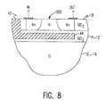
- FIG. 8is a representative SOI resistor (ungated with salicide block mask) 600 .
- the insulator 18 , BOX 12 ′, substrate 14 , first thermally conducting material 44 , and second thermally conducting material 42are shown as in FIG. 2 .
- FIG. 9is a representative double gate SOI MOSFET with thermal sink (contact out of the plane) 700 .
- the insulator 18 , BOX 12 ′, substrate 14 , and first thermally conducting material 44are shown as in FIG. 2 .
- FIG. 10is a representative SOI capacitor (or gated resistor) with thermal sink (contact out of the plane) 800 having a polysilicon film 106 deposited thereon, and spacers 102 contacting the polysilicon film 106 .
- the insulator 18 , BOX 12 ′, substrate 14 , and first thermally conducting material 44are shown as in FIG. 2 .
- FIG. 11is a representative SOI resistor (ungated with salicide block mask, with contact out of the plane) 900 .
- the insulator 18 , BOX 12 ′, substrate 14 , and first thermally conducting material 44are shown as in FIG. 2 .
Landscapes
- Engineering & Computer Science (AREA)
- Microelectronics & Electronic Packaging (AREA)
- Condensed Matter Physics & Semiconductors (AREA)
- General Physics & Mathematics (AREA)
- Computer Hardware Design (AREA)
- Physics & Mathematics (AREA)
- Power Engineering (AREA)
- Manufacturing & Machinery (AREA)
- Chemical & Material Sciences (AREA)
- Materials Engineering (AREA)
- Crystallography & Structural Chemistry (AREA)
- Thin Film Transistor (AREA)
- Semiconductor Integrated Circuits (AREA)
Abstract
Description
Claims (32)
Priority Applications (6)
| Application Number | Priority Date | Filing Date | Title |
|---|---|---|---|
| US09/514,106US6288426B1 (en) | 2000-02-28 | 2000-02-28 | Thermal conductivity enhanced semiconductor structures and fabrication processes |
| KR1020010006935AKR100562241B1 (en) | 2000-02-28 | 2001-02-13 | Thermal conductivity enhanced semiconductor structures and fabrication processes |
| TW090103706ATW480567B (en) | 2000-02-28 | 2001-02-19 | Thermal conductivity enhanced semiconductor structures and fabrication processes |
| JP2001048615AJP4336053B2 (en) | 2000-02-28 | 2001-02-23 | Thermally conductive semiconductor structure and manufacturing method thereof |
| CNB011108622ACN1241260C (en) | 2000-02-28 | 2001-02-27 | Heat conduction itensified semicondcutor structure and making process |
| US09/862,451US6387742B2 (en) | 2000-02-28 | 2001-05-23 | Thermal conductivity enhanced semiconductor structures and fabrication processes |
Applications Claiming Priority (1)
| Application Number | Priority Date | Filing Date | Title |
|---|---|---|---|
| US09/514,106US6288426B1 (en) | 2000-02-28 | 2000-02-28 | Thermal conductivity enhanced semiconductor structures and fabrication processes |
Related Child Applications (1)
| Application Number | Title | Priority Date | Filing Date |
|---|---|---|---|
| US09/862,451DivisionUS6387742B2 (en) | 2000-02-28 | 2001-05-23 | Thermal conductivity enhanced semiconductor structures and fabrication processes |
Publications (1)
| Publication Number | Publication Date |
|---|---|
| US6288426B1true US6288426B1 (en) | 2001-09-11 |
Family
ID=24045809
Family Applications (2)
| Application Number | Title | Priority Date | Filing Date |
|---|---|---|---|
| US09/514,106Expired - LifetimeUS6288426B1 (en) | 2000-02-28 | 2000-02-28 | Thermal conductivity enhanced semiconductor structures and fabrication processes |
| US09/862,451Expired - Fee RelatedUS6387742B2 (en) | 2000-02-28 | 2001-05-23 | Thermal conductivity enhanced semiconductor structures and fabrication processes |
Family Applications After (1)
| Application Number | Title | Priority Date | Filing Date |
|---|---|---|---|
| US09/862,451Expired - Fee RelatedUS6387742B2 (en) | 2000-02-28 | 2001-05-23 | Thermal conductivity enhanced semiconductor structures and fabrication processes |
Country Status (5)
| Country | Link |
|---|---|
| US (2) | US6288426B1 (en) |
| JP (1) | JP4336053B2 (en) |
| KR (1) | KR100562241B1 (en) |
| CN (1) | CN1241260C (en) |
| TW (1) | TW480567B (en) |
Cited By (40)
| Publication number | Priority date | Publication date | Assignee | Title |
|---|---|---|---|---|
| US6515333B1 (en)* | 2001-04-27 | 2003-02-04 | Advanced Micro Devices, Inc. | Removal of heat from SOI device |
| US20030094708A1 (en)* | 2001-10-26 | 2003-05-22 | Hiroyasu Itou | Semiconductor device and method for manufacturing it |
| US20030183923A1 (en)* | 2000-09-21 | 2003-10-02 | Cambridge Semiconductor Limited | Semiconductor device and method of forming a semiconductor device |
| US6674128B1 (en)* | 2001-04-27 | 2004-01-06 | Advanced Micro Devices, Inc. | Semiconductor-on-insulator device with thermoelectric cooler on surface |
| US6773952B2 (en)* | 2000-09-12 | 2004-08-10 | International Business Machines Corporation | Semiconductor chip structures with embedded thermal conductors and a thermal sink disposed over opposing substrate surfaces |
| WO2005001930A1 (en)* | 2003-06-27 | 2005-01-06 | Koninklijke Philips Electronics N.V. | Integrated circuit with an integrated heat sink |
| US20060043455A1 (en)* | 2004-09-01 | 2006-03-02 | Shubneesh Batra | Multiple-depth STI trenches in integrated circuit fabrication |
| US20060202359A1 (en)* | 2005-02-11 | 2006-09-14 | Wintec Industries, Inc. | Apparatus and method for predetermined component placement to a target platform |
| US20070187844A1 (en)* | 2006-02-10 | 2007-08-16 | Wintec Industries, Inc. | Electronic assembly with detachable components |
| US20070215944A1 (en)* | 2006-03-06 | 2007-09-20 | Futoshi Komatsu | Semiconductor device |
| US20090093065A1 (en)* | 2007-09-10 | 2009-04-09 | Zhong Ding | Aspirating and dispensing small volumes of liquids |
| US20090168821A1 (en)* | 2007-12-31 | 2009-07-02 | Alexander Fang | Thermal shunt for active devices on silicon-on-insulator wafers |
| US20090218682A1 (en)* | 2008-03-03 | 2009-09-03 | Nils Lundberg | Semiconductor chip |
| US20090223548A1 (en)* | 2005-03-14 | 2009-09-10 | Borealis Technical Limited | Thermionic/Thermotunneling Thermo-Electrical Converter |
| US20110141696A1 (en)* | 2009-12-15 | 2011-06-16 | Intersil Americas Inc. | Thermal matching in semiconductor devices using heat distribution structures |
| US20110222252A1 (en)* | 2006-02-10 | 2011-09-15 | Kong-Chen Chen | Electronic assembly with detachable components |
| US20110222253A1 (en)* | 2006-02-10 | 2011-09-15 | Kong-Chen Chen | Electronic assembly with detachable components |
| US20110223695A1 (en)* | 2006-02-10 | 2011-09-15 | Kong-Chen Chen | Electronic assembly with detachable components |
| US20110228506A1 (en)* | 2006-02-10 | 2011-09-22 | Kong-Chen Chen | Electronic assembly with detachable components |
| WO2013032472A1 (en)* | 2011-08-31 | 2013-03-07 | Hewlett-Packard Development Company, L.P. | Thermal shunt |
| US8470682B2 (en) | 2010-12-14 | 2013-06-25 | International Business Machines Corporation | Methods and structures for increased thermal dissipation of thin film resistors |
| US20150294921A1 (en)* | 2014-04-10 | 2015-10-15 | Lakshminarayan Viswanathan | Semiconductor devices with a thermally conductive layer and methods of their fabrication |
| US9171779B2 (en) | 2013-08-29 | 2015-10-27 | Industrial Technology Research Institute | Semiconductor laser structure |
| CN108133963A (en)* | 2017-12-21 | 2018-06-08 | 深圳市晶特智造科技有限公司 | Field-effect tube and preparation method thereof |
| US20180247951A1 (en)* | 2017-02-28 | 2018-08-30 | Toshiba Memory Corporation | Semiconductor memory device and method for manufacturing same |
| US10193634B2 (en) | 2016-09-19 | 2019-01-29 | Hewlett Packard Enterprise Development Lp | Optical driver circuits |
| US10256188B2 (en) | 2016-11-26 | 2019-04-09 | Texas Instruments Incorporated | Interconnect via with grown graphitic material |
| US10366883B2 (en) | 2014-07-30 | 2019-07-30 | Hewlett Packard Enterprise Development Lp | Hybrid multilayer device |
| US10381801B1 (en) | 2018-04-26 | 2019-08-13 | Hewlett Packard Enterprise Development Lp | Device including structure over airgap |
| US10529641B2 (en) | 2016-11-26 | 2020-01-07 | Texas Instruments Incorporated | Integrated circuit nanoparticle thermal routing structure over interconnect region |
| US10658177B2 (en) | 2015-09-03 | 2020-05-19 | Hewlett Packard Enterprise Development Lp | Defect-free heterogeneous substrates |
| US10811334B2 (en) | 2016-11-26 | 2020-10-20 | Texas Instruments Incorporated | Integrated circuit nanoparticle thermal routing structure in interconnect region |
| US20200337184A1 (en)* | 2019-04-18 | 2020-10-22 | Apple Inc. | Support plate thin cladding |
| US10861763B2 (en) | 2016-11-26 | 2020-12-08 | Texas Instruments Incorporated | Thermal routing trench by additive processing |
| US11004680B2 (en) | 2016-11-26 | 2021-05-11 | Texas Instruments Incorporated | Semiconductor device package thermal conduit |
| US11088244B2 (en) | 2016-03-30 | 2021-08-10 | Hewlett Packard Enterprise Development Lp | Devices having substrates with selective airgap regions |
| US20220238409A1 (en)* | 2021-01-25 | 2022-07-28 | Globalfoundries U.S. Inc. | Semiconductor structure having a thermal shunt below a metallization layer and integration schemes |
| US11676880B2 (en) | 2016-11-26 | 2023-06-13 | Texas Instruments Incorporated | High thermal conductivity vias by additive processing |
| US20230238270A1 (en)* | 2022-01-21 | 2023-07-27 | Powerchip Semiconductor Manufacturing Corporation | Semiconductor structure and manufacturing method thereof |
| US11972999B2 (en) | 2021-12-07 | 2024-04-30 | Globalfoundries U.S. Inc. | Unlanded thermal dissipation pillar adjacent active contact |
Families Citing this family (15)
| Publication number | Priority date | Publication date | Assignee | Title |
|---|---|---|---|---|
| US6844236B2 (en)* | 2001-07-23 | 2005-01-18 | Agere Systems Inc. | Method and structure for DC and RF shielding of integrated circuits |
| JP3983019B2 (en)* | 2001-08-24 | 2007-09-26 | シャープ株式会社 | Manufacturing method of substrate having embedded structure and manufacturing method of display device |
| US20070096260A1 (en)* | 2005-10-28 | 2007-05-03 | International Business Machines Corporation | Reduced parasitic and high value resistor and method of manufacture |
| KR100790290B1 (en)* | 2006-12-20 | 2008-01-02 | 동부일렉트로닉스 주식회사 | Electronic cooling element and manufacturing method thereof |
| US7851237B2 (en)* | 2007-02-23 | 2010-12-14 | Infineon Technologies Ag | Semiconductor device test structures and methods |
| US7883956B2 (en)* | 2008-02-15 | 2011-02-08 | International Business Machines Corporation | Method of forming coplanar active and isolation regions and structures thereof |
| US7989824B2 (en)* | 2009-06-03 | 2011-08-02 | Koninklijke Philips Electronics N.V. | Method of forming a dielectric layer on a semiconductor light emitting device |
| US20110140232A1 (en)* | 2009-12-15 | 2011-06-16 | Intersil Americas Inc. | Methods of forming a thermal conduction region in a semiconductor structure and structures resulting therefrom |
| CN102915947B (en)* | 2012-10-09 | 2015-09-30 | 哈尔滨工程大学 | A kind of silicon on insulated substrate formation method for CMOS active pixel sensor |
| CN103872039B (en)* | 2012-12-11 | 2016-04-06 | 中芯国际集成电路制造(上海)有限公司 | The manufacture method of ESD protection circuit |
| KR102171268B1 (en) | 2014-09-30 | 2020-11-06 | 삼성전자 주식회사 | manufacturing method of Hybrid silicon laser |
| US11171086B2 (en) | 2019-12-02 | 2021-11-09 | Renesas Electronics Corporation | Semiconductor device |
| CN112769031B (en)* | 2020-12-31 | 2023-05-16 | 联合微电子中心有限责任公司 | Back integrated active device and preparation method thereof |
| CN113764366B (en)* | 2021-11-05 | 2022-02-11 | 微龛(广州)半导体有限公司 | SOI wafer with high heat dissipation performance and preparation method thereof |
| US20240068879A1 (en)* | 2022-08-26 | 2024-02-29 | Globalfoundries U.S. Inc. | Built-in temperature sensors |
Citations (11)
| Publication number | Priority date | Publication date | Assignee | Title |
|---|---|---|---|---|
| US4402185A (en) | 1982-01-07 | 1983-09-06 | Ncr Corporation | Thermoelectric (peltier effect) hot/cold socket for packaged I.C. microprobing |
| US5040381A (en) | 1990-04-19 | 1991-08-20 | Prime Computer, Inc. | Apparatus for cooling circuits |
| US5229327A (en) | 1990-06-12 | 1993-07-20 | Micron Technology, Inc. | Process for manufacturing semiconductor device structures cooled by Peltier junctions and electrical interconnect assemblies therefor |
| US5313094A (en)* | 1992-01-28 | 1994-05-17 | International Business Machines Corportion | Thermal dissipation of integrated circuits using diamond paths |
| US5403783A (en) | 1992-12-28 | 1995-04-04 | Hitachi, Ltd. | Integrated circuit substrate with cooling accelerator substrate |
| US5508740A (en) | 1993-07-23 | 1996-04-16 | Hamamatsu Photonics K.K. | Solid-state imaging device having temperature sensor |
| US5714791A (en) | 1995-12-22 | 1998-02-03 | International Business Machines Corporation | On-chip Peltier cooling devices on a micromachined membrane structure |
| WO1998044561A1 (en)* | 1997-03-31 | 1998-10-08 | Intel Corporation | A thermal conducting trench in a semiconductor structure and method for forming the same |
| US5824561A (en) | 1994-05-23 | 1998-10-20 | Seiko Instruments Inc. | Thermoelectric device and a method of manufacturing thereof |
| US5864158A (en)* | 1997-04-04 | 1999-01-26 | Advanced Micro Devices, Inc. | Trench-gated vertical CMOS device |
| US5879980A (en)* | 1997-03-24 | 1999-03-09 | Advanced Micro Devices, Inc. | Method of making static random access memory cell having a trench field plate for increased capacitance |
Family Cites Families (6)
| Publication number | Priority date | Publication date | Assignee | Title |
|---|---|---|---|---|
| JP2500630B2 (en)* | 1993-06-25 | 1996-05-29 | 日本電気株式会社 | Semiconductor device |
| US5479048A (en)* | 1994-02-04 | 1995-12-26 | Analog Devices, Inc. | Integrated circuit chip supported by a handle wafer and provided with means to maintain the handle wafer potential at a desired level |
| US5892707A (en)* | 1997-04-25 | 1999-04-06 | Micron Technology, Inc. | Memory array having a digit line buried in an isolation region and method for forming same |
| US5877521A (en)* | 1998-01-08 | 1999-03-02 | International Business Machines Corporation | SOI active pixel cell design with grounded body contact |
| US5994759A (en)* | 1998-11-06 | 1999-11-30 | National Semiconductor Corporation | Semiconductor-on-insulator structure with reduced parasitic capacitance |
| US6323073B1 (en)* | 2001-01-19 | 2001-11-27 | United Microelectronics Corp. | Method for forming doped regions on an SOI device |
- 2000
- 2000-02-28USUS09/514,106patent/US6288426B1/ennot_activeExpired - Lifetime
- 2001
- 2001-02-13KRKR1020010006935Apatent/KR100562241B1/ennot_activeExpired - Fee Related
- 2001-02-19TWTW090103706Apatent/TW480567B/ennot_activeIP Right Cessation
- 2001-02-23JPJP2001048615Apatent/JP4336053B2/ennot_activeExpired - Fee Related
- 2001-02-27CNCNB011108622Apatent/CN1241260C/ennot_activeExpired - Lifetime
- 2001-05-23USUS09/862,451patent/US6387742B2/ennot_activeExpired - Fee Related
Patent Citations (11)
| Publication number | Priority date | Publication date | Assignee | Title |
|---|---|---|---|---|
| US4402185A (en) | 1982-01-07 | 1983-09-06 | Ncr Corporation | Thermoelectric (peltier effect) hot/cold socket for packaged I.C. microprobing |
| US5040381A (en) | 1990-04-19 | 1991-08-20 | Prime Computer, Inc. | Apparatus for cooling circuits |
| US5229327A (en) | 1990-06-12 | 1993-07-20 | Micron Technology, Inc. | Process for manufacturing semiconductor device structures cooled by Peltier junctions and electrical interconnect assemblies therefor |
| US5313094A (en)* | 1992-01-28 | 1994-05-17 | International Business Machines Corportion | Thermal dissipation of integrated circuits using diamond paths |
| US5403783A (en) | 1992-12-28 | 1995-04-04 | Hitachi, Ltd. | Integrated circuit substrate with cooling accelerator substrate |
| US5508740A (en) | 1993-07-23 | 1996-04-16 | Hamamatsu Photonics K.K. | Solid-state imaging device having temperature sensor |
| US5824561A (en) | 1994-05-23 | 1998-10-20 | Seiko Instruments Inc. | Thermoelectric device and a method of manufacturing thereof |
| US5714791A (en) | 1995-12-22 | 1998-02-03 | International Business Machines Corporation | On-chip Peltier cooling devices on a micromachined membrane structure |
| US5879980A (en)* | 1997-03-24 | 1999-03-09 | Advanced Micro Devices, Inc. | Method of making static random access memory cell having a trench field plate for increased capacitance |
| WO1998044561A1 (en)* | 1997-03-31 | 1998-10-08 | Intel Corporation | A thermal conducting trench in a semiconductor structure and method for forming the same |
| US5864158A (en)* | 1997-04-04 | 1999-01-26 | Advanced Micro Devices, Inc. | Trench-gated vertical CMOS device |
Cited By (86)
| Publication number | Priority date | Publication date | Assignee | Title |
|---|---|---|---|---|
| US6773952B2 (en)* | 2000-09-12 | 2004-08-10 | International Business Machines Corporation | Semiconductor chip structures with embedded thermal conductors and a thermal sink disposed over opposing substrate surfaces |
| US7230314B2 (en)* | 2000-09-21 | 2007-06-12 | Cambridge Semiconductor Limited | Semiconductor device and method of forming a semiconductor device |
| US20030183923A1 (en)* | 2000-09-21 | 2003-10-02 | Cambridge Semiconductor Limited | Semiconductor device and method of forming a semiconductor device |
| US6515333B1 (en)* | 2001-04-27 | 2003-02-04 | Advanced Micro Devices, Inc. | Removal of heat from SOI device |
| US6674128B1 (en)* | 2001-04-27 | 2004-01-06 | Advanced Micro Devices, Inc. | Semiconductor-on-insulator device with thermoelectric cooler on surface |
| US6784073B1 (en) | 2001-04-27 | 2004-08-31 | Advanced Micro Devices, Inc. | Method of making semiconductor-on-insulator device with thermoelectric cooler |
| US6791156B2 (en)* | 2001-10-26 | 2004-09-14 | Denso Corporation | Semiconductor device and method for manufacturing it |
| US20030094708A1 (en)* | 2001-10-26 | 2003-05-22 | Hiroyasu Itou | Semiconductor device and method for manufacturing it |
| WO2005001930A1 (en)* | 2003-06-27 | 2005-01-06 | Koninklijke Philips Electronics N.V. | Integrated circuit with an integrated heat sink |
| US20060043455A1 (en)* | 2004-09-01 | 2006-03-02 | Shubneesh Batra | Multiple-depth STI trenches in integrated circuit fabrication |
| US7939394B2 (en) | 2004-09-01 | 2011-05-10 | Micron Technology, Inc. | Multiple-depth STI trenches in integrated circuit fabrication |
| US7354812B2 (en) | 2004-09-01 | 2008-04-08 | Micron Technology, Inc. | Multiple-depth STI trenches in integrated circuit fabrication |
| US20080176378A1 (en)* | 2004-09-01 | 2008-07-24 | Micron Technology, Inc. | Multiple-depth sti trenches in integrated circuit fabrication |
| US8535955B2 (en) | 2005-02-11 | 2013-09-17 | Wintec Industries, Inc. | Method for assembling a multi-component electronic apparatus |
| US8344376B2 (en) | 2005-02-11 | 2013-01-01 | Wintec Industries, Inc. | Apparatus and method for predetermined component placement to a target platform |
| US20110164951A1 (en)* | 2005-02-11 | 2011-07-07 | Wintec Industries, Inc. | Apparatus and method for predetermined component placement to a target platform |
| US20110210329A1 (en)* | 2005-02-11 | 2011-09-01 | Chen Kong C | Apparatus and method for predetermined component placement to a target platform |
| US8530248B2 (en) | 2005-02-11 | 2013-09-10 | Wintec Industries, Inc. | Method for placing a component onto a target platform by an apparatus using a probe |
| US8674523B2 (en) | 2005-02-11 | 2014-03-18 | Wintec Industries, Inc. | Apparatus and method for predetermined component placement to a target platform |
| US9253894B2 (en) | 2005-02-11 | 2016-02-02 | Wintec Industries, Inc. | Electronic assembly with detachable components |
| US20110212549A1 (en)* | 2005-02-11 | 2011-09-01 | Chen Kong C | Apparatus and method for predetermined component placement to a target platform |
| US8350393B2 (en) | 2005-02-11 | 2013-01-08 | Wintec Industries, Inc. | Apparatus and method for predetermined component placement to a target platform |
| US8536572B2 (en) | 2005-02-11 | 2013-09-17 | Wintec Industries, Inc. | Assembled multi-component electronic apparatus using alignment and reference marks |
| US8822238B2 (en) | 2005-02-11 | 2014-09-02 | Wintec Industries, Inc. | Apparatus and method for predetermined component placement to a target platform |
| US7928591B2 (en) | 2005-02-11 | 2011-04-19 | Wintec Industries, Inc. | Apparatus and method for predetermined component placement to a target platform |
| US20060202359A1 (en)* | 2005-02-11 | 2006-09-14 | Wintec Industries, Inc. | Apparatus and method for predetermined component placement to a target platform |
| US20110119907A1 (en)* | 2005-02-11 | 2011-05-26 | Kong-Chen Chen | Apparatus and method for predetermined component placement to a target platform |
| US20110121841A1 (en)* | 2005-02-11 | 2011-05-26 | Kong-Chen Chen | Apparatus and method for predetermined component placement to a target platform |
| US20110119906A1 (en)* | 2005-02-11 | 2011-05-26 | Kong-Chen Chen | Apparatus and method for predetermined component placement to a target platform |
| US20110121293A1 (en)* | 2005-02-11 | 2011-05-26 | Kong-Chen Chen | Apparatus and method for predetermined component placement to a target platform |
| US20090223548A1 (en)* | 2005-03-14 | 2009-09-10 | Borealis Technical Limited | Thermionic/Thermotunneling Thermo-Electrical Converter |
| US8541678B2 (en)* | 2005-03-14 | 2013-09-24 | Borealis Technical Limited | Thermionic/thermotunneling thermo-electrical converter |
| US20110223695A1 (en)* | 2006-02-10 | 2011-09-15 | Kong-Chen Chen | Electronic assembly with detachable components |
| WO2007095100A3 (en)* | 2006-02-10 | 2008-01-31 | Wintec Ind Inc | Electronic assembly with detachable components |
| US20110222252A1 (en)* | 2006-02-10 | 2011-09-15 | Kong-Chen Chen | Electronic assembly with detachable components |
| US20110222253A1 (en)* | 2006-02-10 | 2011-09-15 | Kong-Chen Chen | Electronic assembly with detachable components |
| US20070187844A1 (en)* | 2006-02-10 | 2007-08-16 | Wintec Industries, Inc. | Electronic assembly with detachable components |
| US20110228506A1 (en)* | 2006-02-10 | 2011-09-22 | Kong-Chen Chen | Electronic assembly with detachable components |
| GB2448959B (en)* | 2006-02-10 | 2011-10-26 | Wintec Ind Inc | Electronic assembly with detachable components |
| GB2448959A (en)* | 2006-02-10 | 2008-11-05 | Wintec Ind Inc | Electronic assembly with detachable components |
| US20070215944A1 (en)* | 2006-03-06 | 2007-09-20 | Futoshi Komatsu | Semiconductor device |
| US20090093065A1 (en)* | 2007-09-10 | 2009-04-09 | Zhong Ding | Aspirating and dispensing small volumes of liquids |
| US20090168821A1 (en)* | 2007-12-31 | 2009-07-02 | Alexander Fang | Thermal shunt for active devices on silicon-on-insulator wafers |
| US7639719B2 (en)* | 2007-12-31 | 2009-12-29 | Intel Corporation | Thermal shunt for active devices on silicon-on-insulator wafers |
| KR100991579B1 (en) | 2007-12-31 | 2010-11-04 | 인텔 코오퍼레이션 | Thermal Shunt for Active Devices on Silicon on Insulator Wafers |
| WO2009109235A1 (en)* | 2008-03-03 | 2009-09-11 | Sony Ericsson Mobile Communications Ab | Semiconductor chip |
| US20090218682A1 (en)* | 2008-03-03 | 2009-09-03 | Nils Lundberg | Semiconductor chip |
| US20110141696A1 (en)* | 2009-12-15 | 2011-06-16 | Intersil Americas Inc. | Thermal matching in semiconductor devices using heat distribution structures |
| US8859337B2 (en) | 2009-12-15 | 2014-10-14 | Soitec | Thermal matching in semiconductor devices using heat distribution structures |
| US8470682B2 (en) | 2010-12-14 | 2013-06-25 | International Business Machines Corporation | Methods and structures for increased thermal dissipation of thin film resistors |
| WO2013032472A1 (en)* | 2011-08-31 | 2013-03-07 | Hewlett-Packard Development Company, L.P. | Thermal shunt |
| US9093428B2 (en)* | 2011-08-31 | 2015-07-28 | Hewlett-Packard Development Company, L.P. | Thermal shunt |
| US20140204967A1 (en)* | 2011-08-31 | 2014-07-24 | Di Liang | Thermal Shunt |
| US9171779B2 (en) | 2013-08-29 | 2015-10-27 | Industrial Technology Research Institute | Semiconductor laser structure |
| US9614046B2 (en) | 2014-04-10 | 2017-04-04 | Nxp Usa, Inc. | Semiconductor devices with a thermally conductive layer |
| US20150294921A1 (en)* | 2014-04-10 | 2015-10-15 | Lakshminarayan Viswanathan | Semiconductor devices with a thermally conductive layer and methods of their fabrication |
| US10074588B2 (en) | 2014-04-10 | 2018-09-11 | Nxp Usa, Inc. | Semiconductor devices with a thermally conductive layer and methods of their fabrication |
| US9362198B2 (en)* | 2014-04-10 | 2016-06-07 | Freescale Semiconductor, Inc. | Semiconductor devices with a thermally conductive layer and methods of their fabrication |
| US10366883B2 (en) | 2014-07-30 | 2019-07-30 | Hewlett Packard Enterprise Development Lp | Hybrid multilayer device |
| US11004681B2 (en) | 2015-09-03 | 2021-05-11 | Hewlett Packard Enterprise Development Lp | Defect-free heterogeneous substrates |
| US10658177B2 (en) | 2015-09-03 | 2020-05-19 | Hewlett Packard Enterprise Development Lp | Defect-free heterogeneous substrates |
| US11088244B2 (en) | 2016-03-30 | 2021-08-10 | Hewlett Packard Enterprise Development Lp | Devices having substrates with selective airgap regions |
| US10530488B2 (en) | 2016-09-19 | 2020-01-07 | Hewlett Packard Enterprise Development Lp | Optical driver circuits |
| US10193634B2 (en) | 2016-09-19 | 2019-01-29 | Hewlett Packard Enterprise Development Lp | Optical driver circuits |
| US10861763B2 (en) | 2016-11-26 | 2020-12-08 | Texas Instruments Incorporated | Thermal routing trench by additive processing |
| US10256188B2 (en) | 2016-11-26 | 2019-04-09 | Texas Instruments Incorporated | Interconnect via with grown graphitic material |
| US10529641B2 (en) | 2016-11-26 | 2020-01-07 | Texas Instruments Incorporated | Integrated circuit nanoparticle thermal routing structure over interconnect region |
| US10790228B2 (en) | 2016-11-26 | 2020-09-29 | Texas Instruments Incorporated | Interconnect via with grown graphitic material |
| US10811334B2 (en) | 2016-11-26 | 2020-10-20 | Texas Instruments Incorporated | Integrated circuit nanoparticle thermal routing structure in interconnect region |
| US11676880B2 (en) | 2016-11-26 | 2023-06-13 | Texas Instruments Incorporated | High thermal conductivity vias by additive processing |
| US11004680B2 (en) | 2016-11-26 | 2021-05-11 | Texas Instruments Incorporated | Semiconductor device package thermal conduit |
| US11996343B2 (en) | 2016-11-26 | 2024-05-28 | Texas Instruments Incorporated | Thermal routing trench by additive processing |
| US10566339B2 (en)* | 2017-02-28 | 2020-02-18 | Toshiba Memory Coporation | Semiconductor memory device and method for manufacturing same |
| US20180247951A1 (en)* | 2017-02-28 | 2018-08-30 | Toshiba Memory Corporation | Semiconductor memory device and method for manufacturing same |
| US11672117B2 (en) | 2017-02-28 | 2023-06-06 | Kioxia Corporation | Semiconductor memory device and method for manufacturing same |
| US10923490B2 (en) | 2017-02-28 | 2021-02-16 | Toshiba Memory Corporation | Semiconductor memory device and method for manufacturing same |
| CN108133963B (en)* | 2017-12-21 | 2020-09-01 | 南京溧水高新创业投资管理有限公司 | Field effect transistor and manufacturing method thereof |
| CN108133963A (en)* | 2017-12-21 | 2018-06-08 | 深圳市晶特智造科技有限公司 | Field-effect tube and preparation method thereof |
| US10381801B1 (en) | 2018-04-26 | 2019-08-13 | Hewlett Packard Enterprise Development Lp | Device including structure over airgap |
| US20200337184A1 (en)* | 2019-04-18 | 2020-10-22 | Apple Inc. | Support plate thin cladding |
| US11898808B2 (en)* | 2019-04-18 | 2024-02-13 | Apple Inc. | Support plate thin cladding |
| US20220238409A1 (en)* | 2021-01-25 | 2022-07-28 | Globalfoundries U.S. Inc. | Semiconductor structure having a thermal shunt below a metallization layer and integration schemes |
| US11842940B2 (en)* | 2021-01-25 | 2023-12-12 | Globalfoundries U.S. Inc. | Semiconductor structure having a thermal shunt below a metallization layer and integration schemes |
| US11972999B2 (en) | 2021-12-07 | 2024-04-30 | Globalfoundries U.S. Inc. | Unlanded thermal dissipation pillar adjacent active contact |
| US20230238270A1 (en)* | 2022-01-21 | 2023-07-27 | Powerchip Semiconductor Manufacturing Corporation | Semiconductor structure and manufacturing method thereof |
| US11915969B2 (en)* | 2022-01-21 | 2024-02-27 | Powerchip Semiconductor Manufacturing Corporation | Semiconductor structure and manufacturing method thereof |
Also Published As
| Publication number | Publication date |
|---|---|
| KR100562241B1 (en) | 2006-03-22 |
| KR20010085375A (en) | 2001-09-07 |
| CN1319888A (en) | 2001-10-31 |
| US20010029084A1 (en) | 2001-10-11 |
| JP2001274343A (en) | 2001-10-05 |
| JP4336053B2 (en) | 2009-09-30 |
| US6387742B2 (en) | 2002-05-14 |
| TW480567B (en) | 2002-03-21 |
| CN1241260C (en) | 2006-02-08 |
Similar Documents
| Publication | Publication Date | Title |
|---|---|---|
| US6288426B1 (en) | Thermal conductivity enhanced semiconductor structures and fabrication processes | |
| US11830854B2 (en) | Packaged semiconductor devices including backside power rails and methods of forming the same | |
| US7816231B2 (en) | Device structures including backside contacts, and methods for forming same | |
| KR100323488B1 (en) | Contact structure for vertical chip connection | |
| US9917030B2 (en) | Semiconductor structure and fabrication method thereof | |
| US6921961B2 (en) | Semiconductor device having electrical contact from opposite sides including a via with an end formed at a bottom surface of the diffusion region | |
| US11862561B2 (en) | Semiconductor devices with backside routing and method of forming same | |
| US6294829B1 (en) | Multilayer quadruple gate field effect transistor structure for use in integrated circuit devices | |
| US7704811B2 (en) | Sub-lithographics opening for back contact or back gate | |
| US10896958B2 (en) | Silicon-on-insulator backside contacts | |
| WO2008011210A1 (en) | Semiconductor device with under-filled heat extractor | |
| US20240096805A1 (en) | Semiconductor devices with backside routing and method of forming same | |
| US12394660B2 (en) | Buried power rail after replacement metal gate | |
| US6031269A (en) | Quadruple gate field effect transistor structure for use in integrated circuit devices | |
| US20250140648A1 (en) | Bonding a wafer with a substrate to a wafer with backside interconnect wiring | |
| EP0111651B1 (en) | Semiconductor device comprising dielectric isolation regions | |
| US6432809B1 (en) | Method for improved passive thermal flow in silicon on insulator devices | |
| EP4476764B1 (en) | Semiconductor structure with a buried power rail | |
| TWI818638B (en) | Replacement buried power rail | |
| US20220416048A1 (en) | Semiconductor structure having stacked gates and method of manufacture thereof | |
| US11817497B2 (en) | Vertical field effect transistor inverter with single fin device | |
| US20250142901A1 (en) | Semiconductor devices with embedded backside capacitors | |
| WO2025195679A1 (en) | Semiconductor device with dielectric thermal conductor | |
| JPH1050999A (en) | Semiconductor device and fabrication thereof | |
| JP2002151696A (en) | Mis field effect transistor and manufacturing method thereof |
Legal Events
| Date | Code | Title | Description |
|---|---|---|---|
| AS | Assignment | Owner name:INTERNATIONAL BUSINESS MACHINES CORPORATION, NEW Y Free format text:ASSIGNMENT OF ASSIGNORS INTEREST;ASSIGNORS:GAUTHIER, JR. ROBERT J.;SCHEPIS, DOMINIC J.;TONTI, WILLIAM R.;AND OTHERS;REEL/FRAME:010622/0806;SIGNING DATES FROM 20000217 TO 20000225 | |
| FEPP | Fee payment procedure | Free format text:PAYOR NUMBER ASSIGNED (ORIGINAL EVENT CODE: ASPN); ENTITY STATUS OF PATENT OWNER: LARGE ENTITY | |
| STCF | Information on status: patent grant | Free format text:PATENTED CASE | |
| FEPP | Fee payment procedure | Free format text:PAYER NUMBER DE-ASSIGNED (ORIGINAL EVENT CODE: RMPN); ENTITY STATUS OF PATENT OWNER: LARGE ENTITY Free format text:PAYOR NUMBER ASSIGNED (ORIGINAL EVENT CODE: ASPN); ENTITY STATUS OF PATENT OWNER: LARGE ENTITY | |
| FPAY | Fee payment | Year of fee payment:4 | |
| FPAY | Fee payment | Year of fee payment:8 | |
| REMI | Maintenance fee reminder mailed | ||
| FPAY | Fee payment | Year of fee payment:12 | |
| SULP | Surcharge for late payment | Year of fee payment:11 | |
| AS | Assignment | Owner name:GLOBALFOUNDRIES U.S. 2 LLC, NEW YORK Free format text:ASSIGNMENT OF ASSIGNORS INTEREST;ASSIGNOR:INTERNATIONAL BUSINESS MACHINES CORPORATION;REEL/FRAME:036550/0001 Effective date:20150629 | |
| AS | Assignment | Owner name:GLOBALFOUNDRIES INC., CAYMAN ISLANDS Free format text:ASSIGNMENT OF ASSIGNORS INTEREST;ASSIGNORS:GLOBALFOUNDRIES U.S. 2 LLC;GLOBALFOUNDRIES U.S. INC.;REEL/FRAME:036779/0001 Effective date:20150910 | |
| AS | Assignment | Owner name:WILMINGTON TRUST, NATIONAL ASSOCIATION, DELAWARE Free format text:SECURITY AGREEMENT;ASSIGNOR:GLOBALFOUNDRIES INC.;REEL/FRAME:049490/0001 Effective date:20181127 | |
| AS | Assignment | Owner name:GLOBALFOUNDRIES INC., CAYMAN ISLANDS Free format text:RELEASE BY SECURED PARTY;ASSIGNOR:WILMINGTON TRUST, NATIONAL ASSOCIATION;REEL/FRAME:054636/0001 Effective date:20201117 | |
| AS | Assignment | Owner name:GLOBALFOUNDRIES U.S. INC., NEW YORK Free format text:RELEASE BY SECURED PARTY;ASSIGNOR:WILMINGTON TRUST, NATIONAL ASSOCIATION;REEL/FRAME:056987/0001 Effective date:20201117 |