US6285607B1 - Memory system - Google Patents
Memory systemDownload PDFInfo
- Publication number
- US6285607B1 US6285607B1US09/647,194US64719400AUS6285607B1US 6285607 B1US6285607 B1US 6285607B1US 64719400 AUS64719400 AUS 64719400AUS 6285607 B1US6285607 B1US 6285607B1
- Authority
- US
- United States
- Prior art keywords
- memory
- address
- defective
- devices
- location
- Prior art date
- Legal status (The legal status is an assumption and is not a legal conclusion. Google has not performed a legal analysis and makes no representation as to the accuracy of the status listed.)
- Expired - Lifetime
Links
Images


Classifications
- G—PHYSICS
- G11—INFORMATION STORAGE
- G11C—STATIC STORES
- G11C29/00—Checking stores for correct operation ; Subsequent repair; Testing stores during standby or offline operation
- G11C29/70—Masking faults in memories by using spares or by reconfiguring
- G11C29/88—Masking faults in memories by using spares or by reconfiguring with partially good memories
Definitions
- the present inventionrelates to a memory system.
- the present inventionrelates to a memory system having a plurality of memory devices for storing and retrieving data structures, where the system is arranged and configured so that each data structure is divided into portions which are respectively stored in different memory devices.
- Such memory systemsfor example high performance solid state file storage devices, are already known and are used for storage and retrieval of data structures which are wider than the width of an individual addressable memory location in each individual memory device in the system.
- a memory systemmay have 16 memory devices, each memory device storing 4 bits at each addressable memory location, so that data structures which are 64 bits wide may be stored (each 4 bit portion being stored in a different memory device).
- each data structureis stored in memory space spanning a plurality of memory devices with different portions of the data structure stored at the same address but in different devices.
- the addressis applied simultaneously to each memory device in the memory system.
- memory locationrefers herein to the smallest number of bits or bytes which are independently addressed in each memory device; however, it will also be appreciated that the smallest number of bits that are addressed may be a multiple of the smallest number of bits that can be addressed.
- cellrefers herein to a large plurality of memory locations, typically a cell may store, for example, 512 bytes or 8192 bytes.
- widthwhen applied to a memory device herein refers to the number of bits or bytes in a memory location.
- a memory systemcomprising:
- defect mapping meansassociated with each memory device having a defective location, for recording a representation of the location of the or each defective memory location
- a controllerfor accessing the defect mapping means and for writing data structures to and reading data structures from the memory devices;
- host interface meansfor conveying a host address and associated data structures between a host and the controller
- the systembeing arranged and configured so that data structures are divided into portions which are respectively stored in different memory devices, and, in use, the controller accesses the defect mapping means and thereby generates on a per device basis an address corresponding to a non-defective memory location within that device, whereby different addresses may be applied to different devices.
- a memory system typically having a high usable percentage of memory locationsis obtained because each memory device is treated independently, which has the effect that defective memory locations only reduce the memory capacity of the device in which they are located.
- a controllerfor use with a memory system having a plurality of memory devices, at least one of the devices having a defective memory location, and the system having defect mapping means associated with each memory device having a defective location, where the system is arranged and configured so that each data structure is divided into portions which are respectively stored in different memory devices, the controller being arranged for accessing the defect mapping means and thereby generating on a per device basis an address corresponding to a non-defective memory location within that device, whereby different addresses may be applied to different devices.
- the controlleris arranged to organise the memory locations in each memory device into groups of memory locations (where each group is herein called a cell) so that if any cell contains a defective memory location then the entire cell is considered to be defective.
- a cellgroups of memory locations
- the controllerhas a host address converter for converting the host address to an intermediate address, a translator for accessing the defect mapping means and constructing a memory address for a non-defective memory location for each device using the intermediate address and where necessary the defect mapping means, and a data transfer unit for applying the memory addresses to the respective devices.
- the translatoralso determines the number of data structures which may be transferred in an uninterrupted sequence. Conveniently, an indication of this number may be stored in a register or set of registers.
- the defect mapping meansis in the form of a non-volatile memory such as a PROM (programmable read-only memory); conveniently the defect mapping means for each device having a defective location is located on a single a FLASH EPROM.
- the defect mapping meansmay be located on another type of storage medium such as a magnetic disk, a CD-ROM, or such like.
- the defect mapping meanshas an entry for each cell in each of the memory devices.
- the memory devicesare DRAM devices.
- the memory devicesmay be any convenient type of memory, such as SRAM, EEPROM or FLASH EPROM devices.
- SRAMstatic random access memory
- EEPROMelectrically erasable read-only memory
- FLASH EPROM devicesany convenient type of memory, such as SRAM, EEPROM or FLASH EPROM devices.
- the determined addressesmay be concatenated to form a single address having a plurality of fields.
- FIG. 1is a block diagram of a memory system according to one embodiment of the present invention.
- FIG. 2is a block diagram showing a part of FIG. 1 in greater detail
- FIG. 3illustrates different configurations of defects which may be present in the memory space of the memory system of FIG. 1;
- FIG. 4illustrates the memory space of FIG. 3 subdivided into cells to form a cell map
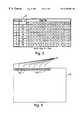
- FIG. 5is a table illustrating a representation of the cell map of FIG. 4;
- FIG. 6illustrates the memory space of a detail of FIG. 1, having data structures stored therein;
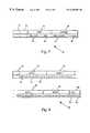
- FIG. 7illustrates the format of a type of address used in the system of FIG. 1;
- FIG. 8illustrates the format of another type of address used in the system of FIG. 1 .
- FIG. 1shows a memory system 10 in accordance with one embodiment of the present invention.
- the system 10is connected to a Personal Computer (PC) 12 (the host) by a standard PC interface 14 .
- PCPersonal Computer
- the system 10has host interface means 16 (in the form of electronic registers) for connecting to the standard PC interface 14 and for conveying a host address and associated data structures between the PC interface 14 and a controller 17 .
- host interface means 16in the form of electronic registers
- the controller 17comprises a host address converter 21 ; a translator 22 having a memory 23 ; and a data transfer unit 24 .
- the controller 17is connected between the host interface means 16 and a memory 18 , and is connected to the memory 18 by a segmented channel 19 and a defect information channel 20 .
- the controller 17has hardware components (which will be described below) but also has software to perform certain translations (as will be described in more detail below).
- the host address converter 21receives a host address and an indication of the amount of data to be transferred.
- the host address converter 21then converts the host address to an intermediate address, which is a physical block address (PBA), and determines the total number of memory access cycles needed to transfer the data.
- PBAphysical block address
- the translator 22receives the PBA from the host address converter 21 and converts it into a memory address which is suitable for accessing memory 18 .
- the data transfer unit 24is hardware which is used to organise and arrange the memory addresses received from the translator 22 so that the memory addresses are suitable for accessing memory 18 ; the data transfer unit 24 also transfers data between memory 18 and host address converter 21 via data bus 25 .
- the memory 18(as best seen in FIG. 2) comprises three memory cards 40 (which may be SIMMs, DIMMs, or such like), each card 40 being populated with sixteen DRAM memory devices 42 for storing data structures generated by the PC 12 (read/write blocks).
- memory cards 40which may be SIMMs, DIMMs, or such like
- each card 40being populated with sixteen DRAM memory devices 42 for storing data structures generated by the PC 12 (read/write blocks).
- Each memory device 42has a memory location width of sixteen bits.
- Each data structureis sixty-four bits wide and the memory 18 is arranged and configured so that there are four slices 44 (each slice 44 comprising four devices 42 in each card 40 ) each slice 44 storing a sixteen bit portion of each data structure at each memory location, so that for each memory location the four slices 44 together store sixty-four bit wide data structures.
- defect mapping means 46in the form of a programmable read-only memory (PROM) may be required to store a representation of the defective locations on that card 40 . In most systems, defect mapping means 46 will be required for each card 40 .
- the memory system 10may perform a memory test cycle to determine which locations in the memory 18 are defective.
- the cards 40may be pre-formatted so that the defect mapping means 46 are programmed to represent the defective memory locations.
- the controllermay update the defect mapping means 46 if locations become defective during operation of the device.
- the segmented channel 19is arranged into four segments, one for each slice 44 .
- the segmented channel 19therefore provides four sets of address lines for addressing the four different slices 44 and four sets of data lines to convey data to and from the four slices 44 , so that each slice 44 can be individually accessed.
- FIG. 3shows the memory space of a device 42 and different configurations of defective locations that may occur within such a device 42 , such as point 50 (i.e. a simple single defective location), small cluster 52 , large cluster 54 , repeating cluster 56 , row 58 and column 60 defects. For clarity, the size of the defective locations has been enlarged relative to the memory space.
- the memory space for each device 42is arranged into a cell map, where the cell map comprises an array of rectangular groups of memory locations called cells 50 , as shown in FIG. 4.
- a cell 50is the minimum addressable unit which can be defined as defective, so where a cell 50 contains a defective location, that cell 50 is considered to be a defective cell 52 .
- FIG. 4shows a sixteen by eight array of cells 50 ; however, the memory space of a device 42 in practical embodiments will usually have a much larger array of cells 50 .
- FIG. 5is a table illustrating a representation of the cell map of FIG. 4 .
- the stream of bitsis shown in a grid pattern corresponding to the cell pattern of FIG. 4 . If a cell 50 is usable then the number zero is inserted in the relevant row and column; however, if a cell is unusable (because it is a defective cell 52 ) then the number one is inserted in the relevant row and column. For example, row zero column zero has a zero because the cell at that position is usable, whereas, row zero column fourteen has a one because the cell at that position is not usable.
- FIG. 5is a table illustrating a representation of the cell map of FIG. 4 .
- the stream of bitsis shown in a grid pattern corresponding to the cell pattern of FIG. 4 .
- Dcell_Ghas an additional column 61 labelled Dcell_G; this column has an entry for each row that indicates the total number of usable cells 50 up to the end of that row. This information (in the Dcell_G column) is useful as an aid in calculating how many usable cells exists below a certain address, as will be described in more detail below.
- the PC 12writes (reads) data blocks to (from) the memory system 10 , these data blocks are typically 512 bytes in size.
- the host address converter 21writes (reads) these data blocks in sixty-four bit wide words (data structures), with sixteen bits of each word being written to (read from) each slice 44 .
- each slicecontains sixty-four addressable locations, each location storing sixteen bits, so that all four slices together store 512 bytes.
- FIG. 6illustrates the address space of a single usable cell 50 having seven portions 62 of data structures stored therein, each portion 62 being sixteen bits in length.
- the portions 62 of data structuresare stored contiguously in one row; the start of each portion 62 being identified in FIG. 6 by reference numeral 64 .
- seven portions 62are shown and these portions are greatly enlarged with respect to the row length; however, once an entire data block has been stored then there will be sixty-four portions 62 stored in each slice 44 .
- the contents of the PROMs 46 (the stream of bits) for each card 40are loaded into memory 23 (FIG. 1) via the defect information channel 20 (FIG. 1 ), which is a serial channel in this embodiment.
- the PC 12writes (reads) a data block to (from) the memory system 10 the PC 12 supplies the memory system 10 with a host address in the form of a logical block address (LBA) corresponding to the data block to be transferred.
- LBAis the logical serial number allocated to that block by the operating system in the PC 12 .
- the PC 12will transfer a sequence of data blocks, in which case the PC 12 provides the address of the first block in the sequence plus the number of logically consecutive blocks in the sequence to be transferred.
- This LBAis conveyed to the host address converter 21 via the PC interface 14 and the host interface 16 , and the host address converter 21 translates the LBA to a physical block address (PBA).
- PBAphysical block address
- the PBAis the start address of a data structure within a data block in defect-free address space.
- This PBAis an intermediate address which indicates the relative position of the first data structure relative to a block, and also indicates the relative position of the first block of the sequence to the blocks in defect-free space.
- the PBArelates to defect-free address space, which is a virtual address space, so the PBA cannot be used to address the memory 18 directly.
- the PBAis the same for all slices 44 because the PBA does not take account of defective cells 52 within slices 44 .
- the ordering of data blocks in physical address spacewill be the same as the ordering of data blocks in logical address space, so the host address converter 21 can convert the LBA to a PBA using a predetermined (software) algorithm which multiplies the LBA by the physical blocksize.
- the number of consecutive logical blocks to be transferredis also translated by the host address converter 21 to the number of data structures contained in the consecutive logical blocks.
- the total number of data structures to be transferredis equivalent to the number of memory access cycles required for the transfer because a data structure is accessed in a single cycle of the memory system 10 .
- the host address converter 21loads an internal total transfer counter 66 with this number (of data structures) and decrements the counter 66 (after each memory access cycle) as the transfer proceeds. When the counter 66 stores the value zero then the transfer of the sequence of data blocks has been completed.
- the host address converter 21may also perform functions such as error checking/correcting code (ECC) generation and checking, and memory refresh control (because DRAM devices require periodic refreshing).
- ECCerror checking/correcting code
- the translator 22performs a translation of the PBA (which is the start address) generated by the host address converter 21 to a (starting) memory address suitable for accessing memory 18 .
- the translator 22determines the maximum number of data structures which can be transferred before the transfer has to be halted (for example, because a defective cell 52 is encountered, or a new memory access cycle is required) and the translator 22 loads burst transfer counters 67 with this number.
- a typical PBAhas the format shown in FIG. 7 .
- the PBA 70has a card field 72 identifying which card 40 in the memory system 10 is being addressed; a device field 74 identifying which device 42 in the card 40 is being addressed; a row field 76 having cell row 78 and row 80 sub-fields; and a column field 82 having cell column 84 and column 86 sub-fields, the row 76 and column 82 fields are for identifying a particular location within the device 42 being addressed.
- the host address converter 21conveys the PBA 70 to the translator 22 via address bus 68 .
- the translator 22constructs a memory system address (MSA) 90 for the PBA 70 .
- the MSA 90is an address for accessing a non-defective region in each slice 44 within the physical memory address space. As the physical memory address space may contain defective regions, the MSA is a complex address having an independent address field for each slice 44 , and these fields may be different for each memory slice 44 .
- a typical MSA 90 for the memory system 10is shown in FIG. 8 and has six fields.
- the first fieldis the card address 72 which identifies which card 40 in the memory system 10 is being addressed, the next four fields are for each slice 44 and the sixth field is for the row and column address within each slice 44 .
- the second field 92is the slice number three address field which has a device sub-field 74 , a cell row sub-field 78 , and a cell column sub-field 84 for identifying the device 42 and cell 50 being addressed within slice number three.
- the third field 94is the slice number two address field
- the fourth field 96is the slice number one address field
- the fifth field 98is the slice number zero address field, each of these fields 94 , 96 , 98 having sub-fields for identifying the device 42 and cell 50 being addressed within the respective field.
- the sixth field 100has two sub-fields, a row sub-field 102 for identifying the row being addressed in each cell 50 and a column sub-field 104 for identifying the column being addressed in each cell 50 .
- Each of the second, third, fourth, and fifth fieldsdefine the address within the respective memory slice to a resolution of one cell; whereas, the sixth field defines the row and column address within each of the cells.
- the same row and column locationis addressed in each cell 50 , even though a different cell 50 may be addressed in each slice 44 .
- the MSA 90will have n+2 fields; although, if the card 72 and cell 100 fields are included in each of the slice fields then there would only be n fields. As an alternative, n different addresses could be generated which together constitute the MSA 90 .
- the translator 22on a per slice basis reads the contents of the memory 23 for the device being accessed and increments the cell column field 84 and if necessary (i.e. if the end of a row is reached) also increments the cell row field 78 of the PBA 70 for each defective cell 52 present in the device at the same or a lower address than the address being accessed. For example, referring to FIG. 4, if the PBA 70 identifies row one column two as the cell to be addressed then the translator 22 constructs a MSA 90 (for the slice represented by FIG.
- the translator 22constructs a MSA 90 identifying row four column one, because there are seven defective cells 52 having the same or a lower address than the original address and one defective cell 52 having an address between the PBA address and the newly-calculated address.
- the translator 22uses the Dcell_G column 61 from the cell map of FIG. 5 as an aid in determining how many cells should be incremented to construct a MSA 90 from a PBA 70 .
- the translator 22determines how many data structures can be written (the data transfer burst length) before the transfer has to be halted and a new MSA 90 calculated.
- the translator 22determines the data transfer burst length by comparing the value of the column field 104 with the total number of columns in a cell 50 . For example, if there are 256 columns in a cell and the column field 104 has a value of 64, then 192 locations can be written to in each slice 44 ; thus 192 data structures (three 512 byte data blocks) can be written before the end of the cell 50 is reached so the data transfer burst length will be at least 192 data structures for the current cell 50 .
- the translator 22determines for each slice 44 the location of the next defective cell 52 , i.e. the defective cell 52 in each slice 44 occurring after the current cell 50 .
- the translator 22also determines how many cells after the current cell can be accessed before a special memory access cycle may be required, for example, a new page access (which may occur when a new row address has to be loaded) for DRAM devices.
- the translator 22compares the number of cells before a defect is reached in one of the slices with the number of cells before a special memory access cycle is required, and chooses the lower of these two as the number of cells which can be accessed in a burst transfer.
- the translator 22When the translator 22 has determined the number of data structures which can be transferred before the transfer has to be halted, then the translator 22 loads internal counters with numbers representing the number of data structures in the first cell addressed by the MSA 90 which can be transferred and, if necessary, the number of cells thereafter which can be accessed before the transfer has to be halted.
- the data transfer burst lengthis 192 data structures and the translator 22 loads burst transfer registers 67 with the number 64 and after each memory access cycle the number in registers 67 is incremented until the number 255 is reached.
- the number in registers 67is used to address the columns in the slices 44 , i.e. the contents of registers 67 is used as the column field 104 , which is incremented after each memory access cycle.
- the translator 22causes the host address converter 21 to stop the total transfer counter 66 .
- the data transfer burst lengthis 192 data structures plus two cells (which have 256 data structures per cell) so the translator 22 loads burst transfer registers 67 so that the number 704 can be counted.
- the registers 67are arranged so that the column field 104 is supplied by the contents of the registers 67 . After each memory access cycle the number in registers 67 is incremented until the number 704 is reached, the translator 22 then causes the host address converter 21 to stop the total transfer counter 66 .
- the data transfer unit 24applies the MSA 90 conveyed by the MSA bus 110 to memory 18 .
- the memory data and address busesare segmented into slices 44 so that a data bus slice relates uniquely to a specific memory slice 44 .
- the translator 22stops the counter 66 and generates a new MSA.
- the data transfer unit 24applies the MSA 90 to each slice 44 in memory 18 and writes [reads] the respective data (having a length corresponding to the data transfer burst) for each slice 44 to [from] the memory 18 .
- the translator 22then constructs a new MSA 90 and determines a new data transfer burst length and applies this new information to the data transfer unit 24 where the writing [reading] procedure is repeated.
- the translator 22increments the row and column addresses of the MSA 90 and where necessary the cell row and cell column addresses.
- the memory system 10provides transfer of data in bursts. These data transfer bursts are synchronised on all of the data slices so that at any time during data transfer a valid sixty-four bit wide data word is present on the four slices 44 ; i.e. valid data words are always present on the full width of the memory system data bus 25 .
- total transfer counter 66When total transfer counter 66 reaches zero then the sequence of data blocks from the PC 12 has been fully transferred.
- additional slicesmay be used for storing control information such as error correcting codes.
- a greater or smaller number of slices than fourmay be used, for example, sixteen slices may be preferred.
- data blocks of size other than 512 bytesmay be used, for example 8192 bytes.
- the address format shown in FIG. 8may be modified for use in a time multiplexed addressing system where the row address is received at one point in time and the column address is received at a different point in time.
- the ordering of physical blocksmay not be the same as the ordering of logical blocks, in which case a look-up table may be used by the host address converter 21 to determine the PBA from the LBA.
- each card 40is considered to be independent so that data blocks are stored entirely on one card 40 rather than partly on one card 40 and partly on another card 40 , thus the card field 72 is identical for all of the slices 44 ; whereas, in other embodiments the card field may not be the same for all slices but the controller 17 may consider the address space as spanned by all of the cards.
- the advantage of independent translation for each cardis that it allows a card to be a replaceable unit, with available memory capacities of slices balanced within each card (so that each slice has a similar capacity), and with a guaranteed minimum memory capacity on each card. It also allows easier relocation of data within a slice if a memory failure occurs during operation. A small amount of spare memory capacity, for example, a few cells, may be allocated within each slice on each card, and data relocation would be required only on a single slice on a single card.
- a hardware pre-sequencermay be used having registers for storing the transfer start address and burst length.
- the pre-sequencermay have registers for storing multiple start addresses and multiple burst lengths so that transfer of data block slices spanning more than one cell 50 may be controlled by hardware in a single uninterrupted operation.
- a new cell addressmay not be generated each time the end of a row in a cell is reached, as other embodiments may determine whether any cell in a slice is the last usable cell in a device and only in that event load a new cell address.
- one or more of the devices in the memorymay not have any defective locations; in such an embodiment, there may be no defect mapping means for that or those devices or the defect mapping means for that or those devices may indicate that there are no defective locations in that or those devices.
- the defect mapping means 46may not be located on the memory card 40 but may be located elsewhere in the memory system 10 .
- the translator 22may only transfer data structures until the end of the cell So is reached. A new cell address is then generated by the translator 22 .
- datais written to and read from the memory 18 in data transfer bursts, where each burst has a maximum length equal to the length of a row within a cell 50 .
- the interface to the memory devicesmay not require an address to be supplied on every memory access cycle, but may supply a burst of data on successive cycles from an initial address. Such a style of interface is easily implemented in the data transfer unit 24 .
Landscapes
- Techniques For Improving Reliability Of Storages (AREA)
- For Increasing The Reliability Of Semiconductor Memories (AREA)
Abstract
Description
Claims (12)
Applications Claiming Priority (3)
| Application Number | Priority Date | Filing Date | Title |
|---|---|---|---|
| GB9806687 | 1998-03-27 | ||
| GBGB9806687.1AGB9806687D0 (en) | 1998-03-27 | 1998-03-27 | Memory system |
| PCT/GB1999/000921WO1999050748A1 (en) | 1998-03-27 | 1999-03-23 | Memory system |
Publications (1)
| Publication Number | Publication Date |
|---|---|
| US6285607B1true US6285607B1 (en) | 2001-09-04 |
Family
ID=10829456
Family Applications (1)
| Application Number | Title | Priority Date | Filing Date |
|---|---|---|---|
| US09/647,194Expired - LifetimeUS6285607B1 (en) | 1998-03-27 | 1999-03-23 | Memory system |
Country Status (3)
| Country | Link |
|---|---|
| US (1) | US6285607B1 (en) |
| GB (2) | GB9806687D0 (en) |
| WO (1) | WO1999050748A1 (en) |
Cited By (43)
| Publication number | Priority date | Publication date | Assignee | Title |
|---|---|---|---|---|
| US6532476B1 (en)* | 1999-11-13 | 2003-03-11 | Precision Solutions, Inc. | Software based methodology for the storage and retrieval of diverse information |
| US20030103626A1 (en)* | 2001-11-30 | 2003-06-05 | Yosef Stein | Programmable data encryption engine |
| US20030126481A1 (en)* | 2001-09-28 | 2003-07-03 | Payne Robert Edwin | Power management system |
| US20030133568A1 (en)* | 2001-12-18 | 2003-07-17 | Yosef Stein | Programmable data encryption engine for advanced encryption standard algorithm |
| US20040199714A1 (en)* | 1995-07-31 | 2004-10-07 | Petro Estakhri | Increasing the memory performance of flash memory devices by writing sectors simultaneously to multiple flash memory devices |
| US6829694B2 (en)* | 2002-02-07 | 2004-12-07 | Analog Devices, Inc. | Reconfigurable parallel look up table system |
| US20050091467A1 (en)* | 2003-10-22 | 2005-04-28 | Robotham Robert E. | Method and apparatus for accessing data segments having arbitrary alignment with the memory structure in which they are stored |
| US20060123325A1 (en)* | 2004-11-22 | 2006-06-08 | James Wilson | Condensed galois field computing system |
| US7102671B1 (en) | 2000-02-08 | 2006-09-05 | Lexar Media, Inc. | Enhanced compact flash memory card |
| US20060221733A1 (en)* | 2005-03-30 | 2006-10-05 | Yang Chang-Lien O | Controller apparatus for utilizing downgrade memory and method for operating the same |
| US7167944B1 (en) | 2000-07-21 | 2007-01-23 | Lexar Media, Inc. | Block management for mass storage |
| US7185208B2 (en) | 2001-09-28 | 2007-02-27 | Lexar Media, Inc. | Data processing |
| US20070094474A1 (en)* | 2005-10-26 | 2007-04-26 | James Wilson | Lookup table addressing system and method |
| US20070094483A1 (en)* | 2005-10-26 | 2007-04-26 | James Wilson | Pipelined digital signal processor |
| US7215580B2 (en) | 2001-09-28 | 2007-05-08 | Lexar Media, Inc. | Non-volatile memory control |
| US7231643B1 (en) | 2002-02-22 | 2007-06-12 | Lexar Media, Inc. | Image rescue system including direct communication between an application program and a device driver |
| US7269615B2 (en) | 2001-12-18 | 2007-09-11 | Analog Devices, Inc. | Reconfigurable input Galois field linear transformer system |
| US7275686B2 (en) | 2003-12-17 | 2007-10-02 | Lexar Media, Inc. | Electronic equipment point-of-sale activation to avoid theft |
| US20080010439A1 (en)* | 2005-10-26 | 2008-01-10 | Yosef Stein | Variable length decoder system and method |
| US7340581B2 (en) | 2001-09-28 | 2008-03-04 | Lexar Media, Inc. | Method of writing data to non-volatile memory |
| US7370166B1 (en) | 2004-04-30 | 2008-05-06 | Lexar Media, Inc. | Secure portable storage device |
| US7441090B2 (en) | 1995-07-31 | 2008-10-21 | Lexar Media, Inc. | System and method for updating data sectors in a non-volatile memory using logical block addressing |
| US7464306B1 (en) | 2004-08-27 | 2008-12-09 | Lexar Media, Inc. | Status of overall health of nonvolatile memory |
| US20090049335A1 (en)* | 2007-08-14 | 2009-02-19 | Dell Products L.P. | System and Method for Managing Memory Errors in an Information Handling System |
| US20090049351A1 (en)* | 2007-08-14 | 2009-02-19 | Dell Products L.P. | Method for Creating a Memory Defect Map and Optimizing Performance Using the Memory Defect Map |
| US20090049257A1 (en)* | 2007-08-14 | 2009-02-19 | Dell Products L.P. | System and Method for Implementing a Memory Defect Map |
| US20090089519A1 (en)* | 2006-03-28 | 2009-04-02 | Dierk Dohmann | Method for memory management and chip cars associated therewith |
| US20090089649A1 (en)* | 2007-09-27 | 2009-04-02 | James Wilson | Programmable compute unit with internal register and bit FIFO for executing Viterbi code |
| US7523249B1 (en) | 1995-07-31 | 2009-04-21 | Lexar Media, Inc. | Direct logical block addressing flash memory mass storage architecture |
| US7594063B1 (en) | 2004-08-27 | 2009-09-22 | Lexar Media, Inc. | Storage capacity status |
| US20090248997A1 (en)* | 2008-03-25 | 2009-10-01 | Horizon Semiconductors Ltd. | De-Interleaving using minimal memory |
| US7634624B2 (en) | 2001-09-28 | 2009-12-15 | Micron Technology, Inc. | Memory system for data storage and retrieval |
| US7725628B1 (en) | 2004-04-20 | 2010-05-25 | Lexar Media, Inc. | Direct secondary device interface by a host |
| US8171203B2 (en) | 1995-07-31 | 2012-05-01 | Micron Technology, Inc. | Faster write operations to nonvolatile memory using FSInfo sector manipulation |
| CN102779557A (en)* | 2011-05-13 | 2012-11-14 | 苏州雄立科技有限公司 | Method and system for data detection and correction of memory module integrated chip |
| US8724408B2 (en) | 2011-11-29 | 2014-05-13 | Kingtiger Technology (Canada) Inc. | Systems and methods for testing and assembling memory modules |
| US20150067248A1 (en)* | 2013-08-30 | 2015-03-05 | Jun Hee Yoo | Dram controller having dram bad page management function and bad page management method thereof |
| KR20150030628A (en)* | 2013-09-12 | 2015-03-20 | 시게이트 테크놀로지 엘엘씨 | Transfer unit management |
| US9117552B2 (en) | 2012-08-28 | 2015-08-25 | Kingtiger Technology(Canada), Inc. | Systems and methods for testing memory |
| US20160259722A1 (en)* | 2015-03-05 | 2016-09-08 | Lite-On Technology Corporation | Region descriptor management method and electronic apparatus thereof |
| US9460815B2 (en) | 2013-12-30 | 2016-10-04 | Sandisk Technologies Llc | Reusing partial bad blocks in NAND memory |
| US9542286B2 (en) | 2014-09-30 | 2017-01-10 | Sandisk Technologies Llc | Failure logging mechanism to reduce garbage collection time in partially reused bad blocks |
| US9678864B2 (en)* | 2014-12-03 | 2017-06-13 | Seagate Technology Llc | Data reallocation upon detection of errors |
Families Citing this family (2)
| Publication number | Priority date | Publication date | Assignee | Title |
|---|---|---|---|---|
| CN1532701B (en)* | 2003-03-20 | 2010-04-28 | 纬创资通股份有限公司 | System for maintaining system stability even though memory is unstable and memory control method |
| US7694195B2 (en)* | 2007-08-14 | 2010-04-06 | Dell Products L.P. | System and method for using a memory mapping function to map memory defects |
Citations (3)
| Publication number | Priority date | Publication date | Assignee | Title |
|---|---|---|---|---|
| US5321697A (en)* | 1992-05-28 | 1994-06-14 | Cray Research, Inc. | Solid state storage device |
| US5544312A (en)* | 1994-04-29 | 1996-08-06 | Intel Corporation | Method of detecting loss of power during block erasure and while writing sector data to a solid state disk |
| US5644539A (en)* | 1991-11-26 | 1997-07-01 | Hitachi, Ltd. | Storage device employing a flash memory |
Family Cites Families (1)
| Publication number | Priority date | Publication date | Assignee | Title |
|---|---|---|---|---|
| GB2312974A (en)* | 1996-05-10 | 1997-11-12 | Memory Corp Plc | Memory replacement |
- 1998
- 1998-03-27GBGBGB9806687.1Apatent/GB9806687D0/ennot_activeCeased
- 1999
- 1999-03-23USUS09/647,194patent/US6285607B1/ennot_activeExpired - Lifetime
- 1999-03-23GBGB0023151Apatent/GB2351822B/ennot_activeExpired - Fee Related
- 1999-03-23WOPCT/GB1999/000921patent/WO1999050748A1/enactiveApplication Filing
Patent Citations (3)
| Publication number | Priority date | Publication date | Assignee | Title |
|---|---|---|---|---|
| US5644539A (en)* | 1991-11-26 | 1997-07-01 | Hitachi, Ltd. | Storage device employing a flash memory |
| US5321697A (en)* | 1992-05-28 | 1994-06-14 | Cray Research, Inc. | Solid state storage device |
| US5544312A (en)* | 1994-04-29 | 1996-08-06 | Intel Corporation | Method of detecting loss of power during block erasure and while writing sector data to a solid state disk |
Cited By (98)
| Publication number | Priority date | Publication date | Assignee | Title |
|---|---|---|---|---|
| US8171203B2 (en) | 1995-07-31 | 2012-05-01 | Micron Technology, Inc. | Faster write operations to nonvolatile memory using FSInfo sector manipulation |
| US8078797B2 (en) | 1995-07-31 | 2011-12-13 | Micron Technology, Inc. | Increasing the memory performance of flash memory devices by writing sectors simultaneously to multiple flash memory devices |
| US8793430B2 (en) | 1995-07-31 | 2014-07-29 | Micron Technology, Inc. | Electronic system having memory with a physical block having a sector storing data and indicating a move status of another sector of the physical block |
| US8554985B2 (en) | 1995-07-31 | 2013-10-08 | Micron Technology, Inc. | Memory block identified by group of logical block addresses, storage device with movable sectors, and methods |
| US20040199714A1 (en)* | 1995-07-31 | 2004-10-07 | Petro Estakhri | Increasing the memory performance of flash memory devices by writing sectors simultaneously to multiple flash memory devices |
| US8397019B2 (en) | 1995-07-31 | 2013-03-12 | Micron Technology, Inc. | Memory for accessing multiple sectors of information substantially concurrently |
| US7424593B2 (en) | 1995-07-31 | 2008-09-09 | Micron Technology, Inc. | Increasing the memory performance of flash memory devices by writing sectors simultaneously to multiple flash memory devices |
| US7774576B2 (en) | 1995-07-31 | 2010-08-10 | Lexar Media, Inc. | Direct logical block addressing flash memory mass storage architecture |
| US20070266201A1 (en)* | 1995-07-31 | 2007-11-15 | Petro Estakhri | Increasing the memory performance of flash memory devices by writing sectors simultaneously to multiple flash memory devices |
| US7441090B2 (en) | 1995-07-31 | 2008-10-21 | Lexar Media, Inc. | System and method for updating data sectors in a non-volatile memory using logical block addressing |
| US9026721B2 (en) | 1995-07-31 | 2015-05-05 | Micron Technology, Inc. | Managing defective areas of memory |
| US7523249B1 (en) | 1995-07-31 | 2009-04-21 | Lexar Media, Inc. | Direct logical block addressing flash memory mass storage architecture |
| US7549013B2 (en) | 1995-07-31 | 2009-06-16 | Lexar Media, Inc. | Increasing the memory performance of flash memory devices by writing sectors simultaneously to multiple flash memory devices |
| US8032694B2 (en) | 1995-07-31 | 2011-10-04 | Micron Technology, Inc. | Direct logical block addressing flash memory mass storage architecture |
| US7263591B2 (en) | 1995-07-31 | 2007-08-28 | Lexar Media, Inc. | Increasing the memory performance of flash memory devices by writing sectors simultaneously to multiple flash memory devices |
| US7908426B2 (en) | 1995-07-31 | 2011-03-15 | Lexar Media, Inc. | Moving sectors within a block of information in a flash memory mass storage architecture |
| US6862599B2 (en) | 1999-11-13 | 2005-03-01 | Kevin D. King | Software-based methodology for the storage and retrieval of diverse information |
| US6532476B1 (en)* | 1999-11-13 | 2003-03-11 | Precision Solutions, Inc. | Software based methodology for the storage and retrieval of diverse information |
| US7102671B1 (en) | 2000-02-08 | 2006-09-05 | Lexar Media, Inc. | Enhanced compact flash memory card |
| US7734862B2 (en) | 2000-07-21 | 2010-06-08 | Lexar Media, Inc. | Block management for mass storage |
| US8019932B2 (en) | 2000-07-21 | 2011-09-13 | Micron Technology, Inc. | Block management for mass storage |
| US8250294B2 (en) | 2000-07-21 | 2012-08-21 | Micron Technology, Inc. | Block management for mass storage |
| US7167944B1 (en) | 2000-07-21 | 2007-01-23 | Lexar Media, Inc. | Block management for mass storage |
| US8386695B2 (en) | 2001-09-28 | 2013-02-26 | Micron Technology, Inc. | Methods and apparatus for writing data to non-volatile memory |
| US20030126481A1 (en)* | 2001-09-28 | 2003-07-03 | Payne Robert Edwin | Power management system |
| US9489301B2 (en) | 2001-09-28 | 2016-11-08 | Micron Technology, Inc. | Memory systems |
| US9032134B2 (en) | 2001-09-28 | 2015-05-12 | Micron Technology, Inc. | Methods of operating a memory system that include outputting a data pattern from a sector allocation table to a host if a logical sector is indicated as being erased |
| US7340581B2 (en) | 2001-09-28 | 2008-03-04 | Lexar Media, Inc. | Method of writing data to non-volatile memory |
| US8694722B2 (en) | 2001-09-28 | 2014-04-08 | Micron Technology, Inc. | Memory systems |
| US8208322B2 (en) | 2001-09-28 | 2012-06-26 | Micron Technology, Inc. | Non-volatile memory control |
| US8135925B2 (en) | 2001-09-28 | 2012-03-13 | Micron Technology, Inc. | Methods of operating a memory system |
| US7185208B2 (en) | 2001-09-28 | 2007-02-27 | Lexar Media, Inc. | Data processing |
| US7944762B2 (en) | 2001-09-28 | 2011-05-17 | Micron Technology, Inc. | Non-volatile memory control |
| US7917709B2 (en) | 2001-09-28 | 2011-03-29 | Lexar Media, Inc. | Memory system for data storage and retrieval |
| US7215580B2 (en) | 2001-09-28 | 2007-05-08 | Lexar Media, Inc. | Non-volatile memory control |
| US7254724B2 (en) | 2001-09-28 | 2007-08-07 | Lexar Media, Inc. | Power management system |
| US7681057B2 (en) | 2001-09-28 | 2010-03-16 | Lexar Media, Inc. | Power management of non-volatile memory systems |
| US7634624B2 (en) | 2001-09-28 | 2009-12-15 | Micron Technology, Inc. | Memory system for data storage and retrieval |
| US7283628B2 (en) | 2001-11-30 | 2007-10-16 | Analog Devices, Inc. | Programmable data encryption engine |
| US20030103626A1 (en)* | 2001-11-30 | 2003-06-05 | Yosef Stein | Programmable data encryption engine |
| US7269615B2 (en) | 2001-12-18 | 2007-09-11 | Analog Devices, Inc. | Reconfigurable input Galois field linear transformer system |
| US20030133568A1 (en)* | 2001-12-18 | 2003-07-17 | Yosef Stein | Programmable data encryption engine for advanced encryption standard algorithm |
| US7508937B2 (en) | 2001-12-18 | 2009-03-24 | Analog Devices, Inc. | Programmable data encryption engine for advanced encryption standard algorithm |
| US6829694B2 (en)* | 2002-02-07 | 2004-12-07 | Analog Devices, Inc. | Reconfigurable parallel look up table system |
| US9213606B2 (en) | 2002-02-22 | 2015-12-15 | Micron Technology, Inc. | Image rescue |
| US8166488B2 (en) | 2002-02-22 | 2012-04-24 | Micron Technology, Inc. | Methods of directly accessing a mass storage data device |
| US7231643B1 (en) | 2002-02-22 | 2007-06-12 | Lexar Media, Inc. | Image rescue system including direct communication between an application program and a device driver |
| US20050091467A1 (en)* | 2003-10-22 | 2005-04-28 | Robotham Robert E. | Method and apparatus for accessing data segments having arbitrary alignment with the memory structure in which they are stored |
| US7275686B2 (en) | 2003-12-17 | 2007-10-02 | Lexar Media, Inc. | Electronic equipment point-of-sale activation to avoid theft |
| US8090886B2 (en) | 2004-04-20 | 2012-01-03 | Micron Technology, Inc. | Direct secondary device interface by a host |
| US7725628B1 (en) | 2004-04-20 | 2010-05-25 | Lexar Media, Inc. | Direct secondary device interface by a host |
| US8316165B2 (en) | 2004-04-20 | 2012-11-20 | Micron Technology, Inc. | Direct secondary device interface by a host |
| US8151041B2 (en) | 2004-04-30 | 2012-04-03 | Micron Technology, Inc. | Removable storage device |
| US8612671B2 (en) | 2004-04-30 | 2013-12-17 | Micron Technology, Inc. | Removable devices |
| US9576154B2 (en) | 2004-04-30 | 2017-02-21 | Micron Technology, Inc. | Methods of operating storage systems including using a key to determine whether a password can be changed |
| US10049207B2 (en) | 2004-04-30 | 2018-08-14 | Micron Technology, Inc. | Methods of operating storage systems including encrypting a key salt |
| US7865659B2 (en) | 2004-04-30 | 2011-01-04 | Micron Technology, Inc. | Removable storage device |
| US7370166B1 (en) | 2004-04-30 | 2008-05-06 | Lexar Media, Inc. | Secure portable storage device |
| US7594063B1 (en) | 2004-08-27 | 2009-09-22 | Lexar Media, Inc. | Storage capacity status |
| US7949822B2 (en) | 2004-08-27 | 2011-05-24 | Micron Technology, Inc. | Storage capacity status |
| US7464306B1 (en) | 2004-08-27 | 2008-12-09 | Lexar Media, Inc. | Status of overall health of nonvolatile memory |
| US7743290B2 (en) | 2004-08-27 | 2010-06-22 | Lexar Media, Inc. | Status of overall health of nonvolatile memory |
| US8296545B2 (en) | 2004-08-27 | 2012-10-23 | Micron Technology, Inc. | Storage capacity status |
| US7512647B2 (en) | 2004-11-22 | 2009-03-31 | Analog Devices, Inc. | Condensed Galois field computing system |
| US20060123325A1 (en)* | 2004-11-22 | 2006-06-08 | James Wilson | Condensed galois field computing system |
| US20060221733A1 (en)* | 2005-03-30 | 2006-10-05 | Yang Chang-Lien O | Controller apparatus for utilizing downgrade memory and method for operating the same |
| US7586779B2 (en)* | 2005-03-30 | 2009-09-08 | Chang-Lien Ou Yang | Controller apparatus for utilizing downgrade memory and method for operating the same |
| US8285972B2 (en) | 2005-10-26 | 2012-10-09 | Analog Devices, Inc. | Lookup table addressing system and method |
| US8024551B2 (en) | 2005-10-26 | 2011-09-20 | Analog Devices, Inc. | Pipelined digital signal processor |
| US7728744B2 (en) | 2005-10-26 | 2010-06-01 | Analog Devices, Inc. | Variable length decoder system and method |
| US20080010439A1 (en)* | 2005-10-26 | 2008-01-10 | Yosef Stein | Variable length decoder system and method |
| US20070094483A1 (en)* | 2005-10-26 | 2007-04-26 | James Wilson | Pipelined digital signal processor |
| US8458445B2 (en) | 2005-10-26 | 2013-06-04 | Analog Devices Inc. | Compute units using local luts to reduce pipeline stalls |
| US20070094474A1 (en)* | 2005-10-26 | 2007-04-26 | James Wilson | Lookup table addressing system and method |
| US20090089519A1 (en)* | 2006-03-28 | 2009-04-02 | Dierk Dohmann | Method for memory management and chip cars associated therewith |
| US8090922B2 (en)* | 2006-03-28 | 2012-01-03 | Vodafone Holding Gmbh | Chip cards and related method for memory management |
| US7945815B2 (en) | 2007-08-14 | 2011-05-17 | Dell Products L.P. | System and method for managing memory errors in an information handling system |
| US20090049335A1 (en)* | 2007-08-14 | 2009-02-19 | Dell Products L.P. | System and Method for Managing Memory Errors in an Information Handling System |
| US20090049257A1 (en)* | 2007-08-14 | 2009-02-19 | Dell Products L.P. | System and Method for Implementing a Memory Defect Map |
| US7949913B2 (en)* | 2007-08-14 | 2011-05-24 | Dell Products L.P. | Method for creating a memory defect map and optimizing performance using the memory defect map |
| US9373362B2 (en)* | 2007-08-14 | 2016-06-21 | Dell Products L.P. | System and method for implementing a memory defect map |
| US20090049351A1 (en)* | 2007-08-14 | 2009-02-19 | Dell Products L.P. | Method for Creating a Memory Defect Map and Optimizing Performance Using the Memory Defect Map |
| US20090089649A1 (en)* | 2007-09-27 | 2009-04-02 | James Wilson | Programmable compute unit with internal register and bit FIFO for executing Viterbi code |
| US8301990B2 (en) | 2007-09-27 | 2012-10-30 | Analog Devices, Inc. | Programmable compute unit with internal register and bit FIFO for executing Viterbi code |
| US20090248997A1 (en)* | 2008-03-25 | 2009-10-01 | Horizon Semiconductors Ltd. | De-Interleaving using minimal memory |
| CN102779557B (en)* | 2011-05-13 | 2015-10-28 | 苏州雄立科技有限公司 | The chip data of integrated memory module detects bearing calibration and system |
| CN102779557A (en)* | 2011-05-13 | 2012-11-14 | 苏州雄立科技有限公司 | Method and system for data detection and correction of memory module integrated chip |
| US8724408B2 (en) | 2011-11-29 | 2014-05-13 | Kingtiger Technology (Canada) Inc. | Systems and methods for testing and assembling memory modules |
| US9224500B2 (en) | 2011-11-29 | 2015-12-29 | Kingtiger Technology (Canada) Inc. | Systems and methods for testing and assembling memory modules |
| US9117552B2 (en) | 2012-08-28 | 2015-08-25 | Kingtiger Technology(Canada), Inc. | Systems and methods for testing memory |
| US9348679B2 (en)* | 2013-08-30 | 2016-05-24 | Samsung Electronics Co., Ltd. | DRAM controller having DRAM bad page management function and bad page management method thereof |
| US20150067248A1 (en)* | 2013-08-30 | 2015-03-05 | Jun Hee Yoo | Dram controller having dram bad page management function and bad page management method thereof |
| KR20150030628A (en)* | 2013-09-12 | 2015-03-20 | 시게이트 테크놀로지 엘엘씨 | Transfer unit management |
| US9460815B2 (en) | 2013-12-30 | 2016-10-04 | Sandisk Technologies Llc | Reusing partial bad blocks in NAND memory |
| US9542286B2 (en) | 2014-09-30 | 2017-01-10 | Sandisk Technologies Llc | Failure logging mechanism to reduce garbage collection time in partially reused bad blocks |
| US9678864B2 (en)* | 2014-12-03 | 2017-06-13 | Seagate Technology Llc | Data reallocation upon detection of errors |
| US20160259722A1 (en)* | 2015-03-05 | 2016-09-08 | Lite-On Technology Corporation | Region descriptor management method and electronic apparatus thereof |
| US9830261B2 (en)* | 2015-03-05 | 2017-11-28 | Lite-On Technology Corporation | Region descriptor management method and electronic apparatus thereof |
Also Published As
| Publication number | Publication date |
|---|---|
| GB2351822B (en) | 2003-01-22 |
| WO1999050748A1 (en) | 1999-10-07 |
| GB2351822A (en) | 2001-01-10 |
| GB9806687D0 (en) | 1998-05-27 |
| GB0023151D0 (en) | 2000-11-01 |
Similar Documents
| Publication | Publication Date | Title |
|---|---|---|
| US6285607B1 (en) | Memory system | |
| US6728860B2 (en) | Address mapping in solid state storage device | |
| US6125072A (en) | Method and apparatus for contiguously addressing a memory system having vertically expanded multiple memory arrays | |
| US6757800B1 (en) | Increasing the memory performance of flash memory devices by writing sectors simultaneously to multiple flash memory devices | |
| US7424593B2 (en) | Increasing the memory performance of flash memory devices by writing sectors simultaneously to multiple flash memory devices | |
| US7013376B2 (en) | Method and system for data block sparing in a solid-state storage device | |
| US6397314B1 (en) | Increasing the memory performance of flash memory devices by writing sectors simultaneously to multiple flash memory devices | |
| KR101573089B1 (en) | Block addressing for parallel memory arrays | |
| US5974564A (en) | Method for remapping defective memory bit sets to non-defective memory bit sets | |
| JP4960705B2 (en) | Adaptive deterministic grouping of blocks into multi-block units | |
| US7404031B2 (en) | Memory card, nonvolatile semiconductor memory, and method of controlling semiconductor memory | |
| US5864568A (en) | Semiconductor memory device for mass storage block access applications | |
| US6430672B1 (en) | Method for performing address mapping using two lookup tables | |
| EP0704801B1 (en) | Memory architecture for solid state disc | |
| US9177668B2 (en) | Method and apparatus for bit cell repair | |
| WO2001061703A2 (en) | Flash eeprom system with simultaneous multiple data sector programming and storage of physical block characteristics in other designated blocks | |
| US5765203A (en) | Storage and addressing method for a buffer memory control system for accessing user and error imformation | |
| US7245539B2 (en) | Memory card, semiconductor device, and method of controlling semiconductor memory | |
| JPH10506212A (en) | Memory management | |
| JP2003505762A (en) | Improved memory system and method |
Legal Events
| Date | Code | Title | Description |
|---|---|---|---|
| AS | Assignment | Owner name:MEMORY CORPORATION PLC, UNITED KINGDOM Free format text:ASSIGNMENT OF ASSIGNORS INTEREST;ASSIGNOR:SINCLAIR, ALAN WELSH;REEL/FRAME:011187/0966 Effective date:20001003 | |
| STCF | Information on status: patent grant | Free format text:PATENTED CASE | |
| AS | Assignment | Owner name:TORRIDON PLC, UNITED KINGDOM Free format text:CHANGE OF NAME;ASSIGNOR:MEMORY CORPORATION PLC;REEL/FRAME:012103/0380 Effective date:20000703 | |
| AS | Assignment | Owner name:MEMQUEST, INC., DELAWARE Free format text:ASSIGNMENT OF ASSIGNORS INTEREST;ASSIGNOR:TORRIDON PLC;REEL/FRAME:012145/0512 Effective date:20000821 | |
| AS | Assignment | Owner name:LEXAR MEDIA, INC., CALIFORNIA Free format text:ASSIGNMENT OF ASSIGNORS INTEREST;ASSIGNOR:MEMQUEST, INC.;REEL/FRAME:013169/0072 Effective date:20020823 | |
| AS | Assignment | Owner name:LEXAR MEDIA, INC., CALIFORNIA Free format text:ASSIGNMENT OF ASSIGNORS INTEREST;ASSIGNORS:SINCLAIR, ALAN WELSH;GOROBETS, AERGEY ANATOLIEVICH;OUPENSKAIA, NATALIA VICTOROVNA;AND OTHERS;REEL/FRAME:014097/0084 Effective date:20020823 | |
| FPAY | Fee payment | Year of fee payment:4 | |
| FPAY | Fee payment | Year of fee payment:8 | |
| FPAY | Fee payment | Year of fee payment:12 | |
| AS | Assignment | Owner name:MICRON TECHNOLOGY, INC., IDAHO Free format text:MERGER;ASSIGNOR:LEXAR MEDIA, INC.;REEL/FRAME:030591/0277 Effective date:20060621 | |
| AS | Assignment | Owner name:U.S. BANK NATIONAL ASSOCIATION, AS COLLATERAL AGENT, CALIFORNIA Free format text:SECURITY INTEREST;ASSIGNOR:MICRON TECHNOLOGY, INC.;REEL/FRAME:038669/0001 Effective date:20160426 Owner name:U.S. BANK NATIONAL ASSOCIATION, AS COLLATERAL AGEN Free format text:SECURITY INTEREST;ASSIGNOR:MICRON TECHNOLOGY, INC.;REEL/FRAME:038669/0001 Effective date:20160426 | |
| AS | Assignment | Owner name:MORGAN STANLEY SENIOR FUNDING, INC., AS COLLATERAL AGENT, MARYLAND Free format text:PATENT SECURITY AGREEMENT;ASSIGNOR:MICRON TECHNOLOGY, INC.;REEL/FRAME:038954/0001 Effective date:20160426 Owner name:MORGAN STANLEY SENIOR FUNDING, INC., AS COLLATERAL Free format text:PATENT SECURITY AGREEMENT;ASSIGNOR:MICRON TECHNOLOGY, INC.;REEL/FRAME:038954/0001 Effective date:20160426 | |
| AS | Assignment | Owner name:U.S. BANK NATIONAL ASSOCIATION, AS COLLATERAL AGENT, CALIFORNIA Free format text:CORRECTIVE ASSIGNMENT TO CORRECT THE REPLACE ERRONEOUSLY FILED PATENT #7358718 WITH THE CORRECT PATENT #7358178 PREVIOUSLY RECORDED ON REEL 038669 FRAME 0001. ASSIGNOR(S) HEREBY CONFIRMS THE SECURITY INTEREST;ASSIGNOR:MICRON TECHNOLOGY, INC.;REEL/FRAME:043079/0001 Effective date:20160426 Owner name:U.S. BANK NATIONAL ASSOCIATION, AS COLLATERAL AGEN Free format text:CORRECTIVE ASSIGNMENT TO CORRECT THE REPLACE ERRONEOUSLY FILED PATENT #7358718 WITH THE CORRECT PATENT #7358178 PREVIOUSLY RECORDED ON REEL 038669 FRAME 0001. ASSIGNOR(S) HEREBY CONFIRMS THE SECURITY INTEREST;ASSIGNOR:MICRON TECHNOLOGY, INC.;REEL/FRAME:043079/0001 Effective date:20160426 | |
| AS | Assignment | Owner name:JPMORGAN CHASE BANK, N.A., AS COLLATERAL AGENT, ILLINOIS Free format text:SECURITY INTEREST;ASSIGNORS:MICRON TECHNOLOGY, INC.;MICRON SEMICONDUCTOR PRODUCTS, INC.;REEL/FRAME:047540/0001 Effective date:20180703 Owner name:JPMORGAN CHASE BANK, N.A., AS COLLATERAL AGENT, IL Free format text:SECURITY INTEREST;ASSIGNORS:MICRON TECHNOLOGY, INC.;MICRON SEMICONDUCTOR PRODUCTS, INC.;REEL/FRAME:047540/0001 Effective date:20180703 | |
| AS | Assignment | Owner name:MICRON TECHNOLOGY, INC., IDAHO Free format text:RELEASE BY SECURED PARTY;ASSIGNOR:U.S. BANK NATIONAL ASSOCIATION, AS COLLATERAL AGENT;REEL/FRAME:047243/0001 Effective date:20180629 | |
| AS | Assignment | Owner name:MICRON TECHNOLOGY, INC., IDAHO Free format text:RELEASE BY SECURED PARTY;ASSIGNOR:MORGAN STANLEY SENIOR FUNDING, INC., AS COLLATERAL AGENT;REEL/FRAME:050937/0001 Effective date:20190731 | |
| AS | Assignment | Owner name:MICRON SEMICONDUCTOR PRODUCTS, INC., IDAHO Free format text:RELEASE BY SECURED PARTY;ASSIGNOR:JPMORGAN CHASE BANK, N.A., AS COLLATERAL AGENT;REEL/FRAME:051028/0001 Effective date:20190731 Owner name:MICRON TECHNOLOGY, INC., IDAHO Free format text:RELEASE BY SECURED PARTY;ASSIGNOR:JPMORGAN CHASE BANK, N.A., AS COLLATERAL AGENT;REEL/FRAME:051028/0001 Effective date:20190731 |