US6285598B1 - Precision programming of nonvolatile memory cells - Google Patents
Precision programming of nonvolatile memory cellsDownload PDFInfo
- Publication number
- US6285598B1 US6285598B1US09/523,828US52382800AUS6285598B1US 6285598 B1US6285598 B1US 6285598B1US 52382800 AUS52382800 AUS 52382800AUS 6285598 B1US6285598 B1US 6285598B1
- Authority
- US
- United States
- Prior art keywords
- memory cell
- programming
- terminal
- integrated circuit
- line
- Prior art date
- Legal status (The legal status is an assumption and is not a legal conclusion. Google has not performed a legal analysis and makes no representation as to the accuracy of the status listed.)
- Expired - Lifetime
Links
- 230000015654memoryEffects0.000titleclaimsabstractdescription234
- 238000000034methodMethods0.000claimsabstractdescription30
- 238000002347injectionMethods0.000claimsabstractdescription21
- 239000007924injectionSubstances0.000claimsabstractdescription21
- 238000007667floatingMethods0.000claimsdescription49
- 230000001419dependent effectEffects0.000claimsdescription16
- 238000012795verificationMethods0.000claimsdescription9
- 241000701502Carnation etched ring virusSpecies0.000description15
- 239000002784hot electronSubstances0.000description9
- 230000005684electric fieldEffects0.000description7
- XUIMIQQOPSSXEZ-UHFFFAOYSA-NSiliconChemical compound[Si]XUIMIQQOPSSXEZ-UHFFFAOYSA-N0.000description5
- 230000008859changeEffects0.000description5
- 238000013461designMethods0.000description5
- 229910052710siliconInorganic materials0.000description5
- 239000010703siliconSubstances0.000description5
- VYPSYNLAJGMNEJ-UHFFFAOYSA-NSilicium dioxideChemical compoundO=[Si]=OVYPSYNLAJGMNEJ-UHFFFAOYSA-N0.000description4
- 238000010586diagramMethods0.000description4
- 239000004065semiconductorSubstances0.000description4
- 238000012545processingMethods0.000description3
- 238000013459approachMethods0.000description2
- 230000008901benefitEffects0.000description2
- 238000005516engineering processMethods0.000description2
- 230000007246mechanismEffects0.000description2
- 230000008569processEffects0.000description2
- 235000012239silicon dioxideNutrition0.000description2
- 239000000377silicon dioxideSubstances0.000description2
- 230000001052transient effectEffects0.000description2
- 239000000969carrierSubstances0.000description1
- 230000008878couplingEffects0.000description1
- 238000010168coupling processMethods0.000description1
- 238000005859coupling reactionMethods0.000description1
- 230000007423decreaseEffects0.000description1
- 238000009792diffusion processMethods0.000description1
- 230000000694effectsEffects0.000description1
- 230000006870functionEffects0.000description1
- 238000012986modificationMethods0.000description1
- 230000004048modificationEffects0.000description1
- 230000009467reductionEffects0.000description1
- 229920006395saturated elastomerPolymers0.000description1
- 238000012163sequencing techniqueMethods0.000description1
- 238000012358sourcingMethods0.000description1
- 230000002459sustained effectEffects0.000description1
- 230000005641tunnelingEffects0.000description1
Images


Classifications
- G—PHYSICS
- G11—INFORMATION STORAGE
- G11C—STATIC STORES
- G11C16/00—Erasable programmable read-only memories
- G11C16/02—Erasable programmable read-only memories electrically programmable
- G11C16/06—Auxiliary circuits, e.g. for writing into memory
- G11C16/34—Determination of programming status, e.g. threshold voltage, overprogramming or underprogramming, retention
- G11C16/3436—Arrangements for verifying correct programming or erasure
- G11C16/3454—Arrangements for verifying correct programming or for detecting overprogrammed cells
- G11C16/3459—Circuits or methods to verify correct programming of nonvolatile memory cells
- G—PHYSICS
- G11—INFORMATION STORAGE
- G11C—STATIC STORES
- G11C16/00—Erasable programmable read-only memories
- G11C16/02—Erasable programmable read-only memories electrically programmable
- G11C16/04—Erasable programmable read-only memories electrically programmable using variable threshold transistors, e.g. FAMOS
- G—PHYSICS
- G11—INFORMATION STORAGE
- G11C—STATIC STORES
- G11C11/00—Digital stores characterised by the use of particular electric or magnetic storage elements; Storage elements therefor
- G11C11/56—Digital stores characterised by the use of particular electric or magnetic storage elements; Storage elements therefor using storage elements with more than two stable states represented by steps, e.g. of voltage, current, phase, frequency
- G11C11/5621—Digital stores characterised by the use of particular electric or magnetic storage elements; Storage elements therefor using storage elements with more than two stable states represented by steps, e.g. of voltage, current, phase, frequency using charge storage in a floating gate
- G11C11/5628—Programming or writing circuits; Data input circuits
- G—PHYSICS
- G11—INFORMATION STORAGE
- G11C—STATIC STORES
- G11C11/00—Digital stores characterised by the use of particular electric or magnetic storage elements; Storage elements therefor
- G11C11/56—Digital stores characterised by the use of particular electric or magnetic storage elements; Storage elements therefor using storage elements with more than two stable states represented by steps, e.g. of voltage, current, phase, frequency
- G11C11/5621—Digital stores characterised by the use of particular electric or magnetic storage elements; Storage elements therefor using storage elements with more than two stable states represented by steps, e.g. of voltage, current, phase, frequency using charge storage in a floating gate
- G11C11/5642—Sensing or reading circuits; Data output circuits
- G—PHYSICS
- G11—INFORMATION STORAGE
- G11C—STATIC STORES
- G11C16/00—Erasable programmable read-only memories
- G11C16/02—Erasable programmable read-only memories electrically programmable
- G11C16/06—Auxiliary circuits, e.g. for writing into memory
- G11C16/10—Programming or data input circuits
- G—PHYSICS
- G11—INFORMATION STORAGE
- G11C—STATIC STORES
- G11C16/00—Erasable programmable read-only memories
- G11C16/02—Erasable programmable read-only memories electrically programmable
- G11C16/06—Auxiliary circuits, e.g. for writing into memory
- G11C16/34—Determination of programming status, e.g. threshold voltage, overprogramming or underprogramming, retention
- G11C16/3436—Arrangements for verifying correct programming or erasure
- G11C16/3454—Arrangements for verifying correct programming or for detecting overprogrammed cells
- G—PHYSICS
- G11—INFORMATION STORAGE
- G11C—STATIC STORES
- G11C16/00—Erasable programmable read-only memories
- G11C16/02—Erasable programmable read-only memories electrically programmable
- G11C16/06—Auxiliary circuits, e.g. for writing into memory
- G11C16/34—Determination of programming status, e.g. threshold voltage, overprogramming or underprogramming, retention
- G11C16/3436—Arrangements for verifying correct programming or erasure
- G11C16/3468—Prevention of overerasure or overprogramming, e.g. by verifying whilst erasing or writing
- G—PHYSICS
- G11—INFORMATION STORAGE
- G11C—STATIC STORES
- G11C27/00—Electric analogue stores, e.g. for storing instantaneous values
- G11C27/005—Electric analogue stores, e.g. for storing instantaneous values with non-volatile charge storage, e.g. on floating gate or MNOS
- G—PHYSICS
- G11—INFORMATION STORAGE
- G11C—STATIC STORES
- G11C2211/00—Indexing scheme relating to digital stores characterized by the use of particular electric or magnetic storage elements; Storage elements therefor
- G11C2211/56—Indexing scheme relating to G11C11/56 and sub-groups for features not covered by these groups
- G11C2211/562—Multilevel memory programming aspects
- G11C2211/5621—Multilevel programming verification
- G—PHYSICS
- G11—INFORMATION STORAGE
- G11C—STATIC STORES
- G11C2211/00—Indexing scheme relating to digital stores characterized by the use of particular electric or magnetic storage elements; Storage elements therefor
- G11C2211/56—Indexing scheme relating to G11C11/56 and sub-groups for features not covered by these groups
- G11C2211/562—Multilevel memory programming aspects
- G11C2211/5622—Concurrent multilevel programming of more than one cell
- G—PHYSICS
- G11—INFORMATION STORAGE
- G11C—STATIC STORES
- G11C2211/00—Indexing scheme relating to digital stores characterized by the use of particular electric or magnetic storage elements; Storage elements therefor
- G11C2211/56—Indexing scheme relating to G11C11/56 and sub-groups for features not covered by these groups
- G11C2211/564—Miscellaneous aspects
- G11C2211/5645—Multilevel memory with current-mirror arrangements
- G—PHYSICS
- G11—INFORMATION STORAGE
- G11C—STATIC STORES
- G11C7/00—Arrangements for writing information into, or reading information out from, a digital store
- G11C7/10—Input/output [I/O] data interface arrangements, e.g. I/O data control circuits, I/O data buffers
- G11C7/1048—Data bus control circuits, e.g. precharging, presetting, equalising
Definitions
- This inventionrelates in general to semiconductor memories and, in particular, to the programming of nonvolatile semiconductor memories.
- Nonvolatile semiconductor memory integrated circuitssuch as EEPROM, EPROM, and FLASH, have traditionally been used to store a single digital bit per memory cell, which is termed hereafter as single bit storage.
- Memories capable of storing more than one bit of digital data per memory cell and their benefitshave been described previously and are called multilevel memories.
- a levelrepresents a specific range of electrical charge stored in each memory cell.
- To store N bits per memory cellrequires 2 N discrete levels. Each discrete level corresponds to a unique binary data pattern for all N bits. The cell is erased or programmed to store charge within one of these 2 N discrete levels.
- Sensing circuitsdetermine which level of charge is stored in the cell and read out the corresponding binary data pattern stored for the N bits. Digital information can thus be stored at a significantly lower cost per bit since N times the number of bits can be stored in the same memory cell array area previously storing just a single bit per cell.
- Nonvolatile semiconductor memory integrated circuits using EEPROM and FLASH memory cellshave also been used to store analog information.
- the amount of electrical charge stored in each memory cellis part of a continuum instead of discrete multiple levels.
- the precision of the stored chargedetermines the signal-to-noise ratio of the analog information.
- EEPROM, EPROM, and FLASH memory cellsare typically based on silicon gate MOS transistor technology.
- Such a nonvolatile memory cell 100is shown in FIG. 1 .
- Chargeis stored on a piece of silicon which is called a floating gate 105 .
- This gateis completely surrounded by silicon dioxide which, ideally, can only pass charge during program or erase operations and so is called “floating”.
- the floating gate 105is formed near a silicon channel 110 between a source 115 and a drain 120 diffusion regions.
- the floating gate 105 voltageis determined by the amount of charge stored and by the adjacent capacitive coupling to a control gate 125 , source 115 , drain 120 , and channel 110 .
- the conductivity of the silicon channel 110is controlled by the floating gate 105 voltage in an similar manner as in a classic MOS transistor.
- Nonvolatile memory cell programmingrequires charge passage through an oxide 130 to the floating gate 105 and is accomplished via two mechanisms; tunneling and hot carrier injection.
- Hot carriersin the case of an n-channel device, are electrons with sufficient energy to conduct through silicon dioxide.
- Hot electron programmingrequires two basic conditions to be met. First, a source of hot electrons must be generated in the channel 110 . This is accomplished by creating a high electric field region, Eh 135 , in the channel 110 to accelerate the electrons to an energy sufficient to make them “hot”. In FIG. 1 the flow of electrons in the channel 110 is represented by a source current, Is 140 , and a drain current, Id 145 . Second, a vertical electric field, Ev 150 , between the floating gate 105 and channel 110 must attract the hot electrons toward the floating gate 105 . The hot electrons which flow to the floating gate 105 create a floating gate charging current, Ig 155 .
- FIGS. 2A-2Dshows some examples of such cells.
- CHEIChannel Hot Electron Injection
- HESSCHEIHigh Efficiency Source Side Channel Hot Electron Injection
- SSISource Side Injection
- the read or verify sensing stepsmust be accomplished with adequate precision to halt the programming algorithm at the desired level in the case of multilevel and at the correct charge state for analog storage.
- Various sensing approacheshave been described and can be generally divided into two modes of operation.
- current-mode sensingthe current flowing in the cell is dependent on the charge stored in the cell.
- the cellis biased by applying voltages and a current flowing in the cell is sensed.
- voltage-mode sensingthe current flowing in the cell is not dependent on the charge stored in the cell.
- the cellis biased by applying a fixed current and a voltage is sensed which corresponds uniquely to the amount of charge stored on the floating gate of the cell.
- Hot carrier injection programming in present technologiestakes place quickly in the range of 0.5 to 5 microseconds. This is due to the high programming voltages which generate high cell channel currents Is 140 and Id 145 , some of which is sent towards the floating gate 105 . This fast programming makes it difficult to maintain precision for multilevel and analog applications.
- the high currentposes power problems which may prevent the use of a single power supply voltage for the chip. It also restricts the number of cells which can be simultaneously programmed in a “page” of cells. Methods to reduce the programming current have been proposed at the expense of adding extra processing complexity to the cell.
- a memory circuit according to the present inventioncontrols the programming current directly and accomplishes a high degree of programming precision.
- the present inventionprovides for an integrated circuit memory system and method for the precision programming of single or a plurality of nonvolatile memory cells.
- the inventionenables each memory cell to either have a stored charge in one of a plurality of discrete levels corresponding to digital information or have a stored charge as part of a continuum corresponding to analog information.
- Precision programmingis achieved by directly controlling the current flowing between source and drain in the memory cell during hot carrier injection programming, thereby allowing reduced programming cell current and lower power operation.
- the reduced cell currentenables a plurality of cells to be programmed simultaneously in a page of cells which improves programming time, requires only a single power supply, and does not require additional silicon processing steps.
- Multiple program and verify cyclesare performed with incrementally changing programming cell current during successive cycles to reduce programming time.
- the application of programming, verify or read cell voltages and currentare performed in a predetermined manner including pre-charging the bitline depending on the characteristics of the particular memory cell type used.
- parts of the bitline driverdo not require the use of high voltage circuitry which reduces circuit complexity.
- the use of voltage-mode sensingallows exactly the same circuit topology to be used for programming as for sensing operations further simplifying the circuit complexity.
- An alternative embodiment of the inventionuses a pre-charge voltage control circuit to indirectly control the current in the memory cell while the current control circuit is turned off during programming.
- FIG. 1is a generalized description of the principles of hot carrier injection programming in a nonvolatile memory cell as is known in the prior art.
- FIGS. 2A-2Dshow four prior art examples of various cell process designs which program on the principle of hot carrier injection.
- FIG. 3is a generalized description of the principles of hot carrier injection programming in a nonvolatile memory cell used in accordance with the teachings or one embodiment of the present invention.
- FIG. 4is a block diagram of a preferred embodiment of this invention.
- FIG. 5Ashows details of one embodiment of this invention during a programming cycle.
- FIG. 5Bshows details of one embodiment of this invention during a verify or read cycle.
- FIG. 6shows details of one alternative embodiment of this invention during a programming cycle.
- FIG. 7is a block diagram of one embodiment of this invention utilizing a memory cell array in page mode operation.
- a memory integrated circuittakes direct control of the channel 110 current during programming. By controlling that current directly, a high degree of programming precision is obtained.
- the circuits and methods describedare applicable to a variety of cell process designs which program on the principle of hot carrier injection.
- FIG. 3shows a nonvolatile memory cell 300 which programs by hot carrier injection.
- the cellis n-channel and the cell is programmed by adding electrons to a floating gate 305 . It should be obvious to those skilled in the art of nonvolatile memories that holes would be added to the floating gate 305 if the cell were of p-channel type.
- the cell shown in FIG. 3is only a simplified representation showing only those features essential to the discussion and does not limit the applicability of this invention to other types of cell structures that also use hot carrier injection for programming.
- a control gate 325 shown in FIG. 3may represent a plurality of control gates in some cell designs.
- the flow of electrons in a channel 310 from a source 315 to a drain 320is represented by a source current, Is 340 , and a drain current, Id 345 .
- a source currentIs 340
- a drain currentId 345 .
- Eh 335a high electric field region
- Ev 350attracts some of the hot electrons through an oxide 330 to the floating gate 305 .
- the electrons flowing to the floating gate 305create a floating gate 305 charging current, Ig 355 .
- the floating gate charging current Ig 355is small in comparison to either Is 340 or Id 345 . Therefore Is 340 and Id 345 are approximately equal.
- the number of electrons entering the high electric field region, Eh 335is directly related to Is 340 and Id 345 . A portion of the electrons entering that region will become the hot electrons forming the floating gate charging current, Ig 355 .
- Ig 355is proportional to Is 340 and Id 345 . For instance, reducing Is 340 or Id 345 during programming will reduce Ig 355 .
- Ig 355can be assumed constant only for small amounts of charge change on the floating gate 305 which would be the case when Ig 355 is small or for a short programming time. Assuming Ig 355 stays constant during programming, the change in the charge stored on the floating gate 305 is directly related to Ig 355 times the programming time.
- Multilevel and analog memory applicationsrequire a high degree of precision in the amount of charge change on the floating gate 305 . This can be obtained by approaching the desired charge level in small increments. A series of programming pulse and verify steps can accomplish this incremental programming approach if the amount of charge change with each pulse is small. For practical reasons, the shortest programming pulse time has a lower bound. Under ordinary conditions of hot carrier programming, that shortest pulse time usually changes the charge too much to be useful for the precision desired. Thus, to obtain a small charge change on the floating gate 305 during an individual programming pulse, Ig 355 must be reduced. This invention accomplishes that Ig 355 reduction by directly reducing the Is 340 or Id 345 . The cell's programming rate is reduced to obtain a high degree of programming precision which is required for multilevel digital storage or analog information storage.
- the vertical electric field Ev 350decreases, causing lower Ig 355 and slower programming.
- This inventionaccomplishes that by increasing Is 340 or Id 345 with successive programming pulses.
- the precision programming by this inventionis accomplished without adding extra cell processing steps.
- the reduced programming cell currentallows many cells to be programmed simultaneously in a page of cells which offsets the slower programming rate.
- the resulting programming performance of the memory chip using this inventionis improved while preserving the multilevel capability which reduces the chip's cost relative to single bit per cell memories.
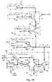
- FIG. 4The major blocks of a preferred embodiment of the present invention are shown in FIG. 4 . These blocks are connected to a memory cell 45 to achieve erase, programming, verifying and reading. It is assumed that the memory cell 45 consists of a type of non-volatile memory cell which can be programmed using the hot carrier injection phenomenon. It is also assumed that during sensing for verify or read, the memory cell 45 is placed in the voltage-mode. The memory cell 45 can also be placed in a mode other than voltage-mode during verify and read.
- a CL line 42connects one terminal of the memory cell 45 to a common-line voltage control circuit block 41 .
- the CL line 42is normally shared amongst a plurality of memory cells in single or multiple rows or can be shared by all the memory cells in the memory array.
- the CL line 42is shared amongst a plurality of memory cells in a column or a memory array.
- the common-line voltage control circuit block 41provides the appropriate voltage at the CL line 42 during the erase, program, verify and read of the memory cell 45 under the control of a erase, program, verify & read control circuit block 414 .
- the erase, program verify & read control circuit block 414consists of the necessary control and sequencing logic to accomplish the erasing, programming, verifying and reading of the memory cell.
- a CG line 43connects the memory cell 45 to the control-gate voltage control circuit block 44 .
- the CG line 43is normally shared amongst a plurality of memory cells in a row of a memory array.
- the control-gate voltage control circuit block 44provides the appropriate voltage at the CG line 43 during erase, program, verify and read of the memory cell, under the control of the erase, program, verify & read control circuit block 414 .
- a BL line 415connects the memory cell to a bitline selection circuit block 46 .
- the BL line 415is shared amongst a plurality of memory cells in a column of a memory array.
- the CL line 42 and the BL line 415run parallel and adjacent to each other.
- the bitline selection circuit block 46either couples or decouples the BL line 415 from a VR line 48 .
- a pre-charge voltage control circuit block 404 connected to the VR line 48pre-charges the VR line 48 during programming, verifying and reading of the memory cell 45 .
- a pre-charge voltage generation block 410has the capability to provide different amounts of pre-charge voltages to the pre-charge voltage control circuit block 404 , under the control of the erase, program, verify & read control circuit block 414 .
- the VPCHGEN line 406connects the pre-charge voltage control circuit block 404 to the pre-charge voltage generation block 410 .
- a current control circuit block 403 connected to the VR line 48causes a programming current pulse to pass through the memory cell 45 during programming and a constant current to pass through the memory cell 45 during verifying or reading.
- the current control circuit block 403has a latch driven by a logic output line 402 .
- the latchis reset if the logic output line 402 goes to a logic low during verify or read.
- the latchis set by the erase, program, verify & read control circuit block 414 .
- the latchis set and is independent of the logic output line 402 .
- the current control circuit block 403passes either the programming current pulse during programming or constant current during verify or read.
- An IGEN line 407connects the current control circuit block 403 to a bitline current generation block 411 .
- the bitline current generation block 411controls the magnitude of the programming current pulse passing through the memory cell 45 during programming and also the magnitude of the constant current passing through the memory cell 45 during verifying and reading.
- the erase, program, verify & read control circuit block 414also controls the duration of the programming current pulse passing through the memory cell 45 during programming.
- a CERV line 408connects the current control circuit block 403 to a current end reference voltage circuit block 412 .
- the current end reference voltage circuit block 412provides the appropriate voltage to allow the current control circuit block 403 to either sink or source current through the memory cell 45 either during the application of the programming current pulse while programming or during the application of the constant current while verifying or reading. If the current control circuit block 403 sinks current through the memory cell 45 , the voltage on the CERV line 408 provided by the current end reference voltage circuit block 412 is lower in magnitude with respect to the voltage provided by the common-line voltage control circuit block 41 .
- the current end reference voltage circuit block 412provides 0V on the CERV line 408 and the common-line voltage control circuit block 41 provides higher voltage on the CL line 42 . If the current control circuit block 403 sources current to the memory cell 45 , the voltage provided by the current end reference voltage circuit block 412 on the CERV line 408 is higher in magnitude with respect to the voltage provided by the common-line voltage control circuit block 41 on the CL line 42 . For example, the current end reference voltage circuit block 412 provides high voltage on the CERV line 408 and the common-line voltage control circuit block 41 provides 0V when the current control circuit sources current to the memory cell 45 .
- the difference between voltages provided by the current end reference voltage circuit block 412 on the CERV line 408 and that provided by the common-line voltage control circuit block 41 on the CL line 42 , either in the current sinking or the current sourcing case,is large enough to create the necessary conditions for hot electrons to be generated.
- the reference voltagesare provided to the reference voltage selection circuit block 405 by a reference voltage generation block 413 via a RVGEN bus 409 .
- the pre-charge voltage control circuit block 404 , current control circuit block 403 , voltage comparator 49 , reference voltage selection circuit block 405 , logic output line 402 , and VREF line 401together form a bitline driver block 416 , as shown in FIG. 4 .
- an ordered sequence of eventshave to happen under the control of the erase, program, verify & read control circuit block 414 .
- the memory cell 45is erased through an erase cycle, by applying the appropriate voltages at the CL line 42 , the CG line 43 and the BL line 415 .
- Erasehere means the removal of electrons from the floating gate of the memory cell 45 .
- an erase verification cycleis performed in order to verify whether the memory cell 45 has been erased properly.
- An erased cellwill normally verify or read back a voltage on the VR line 48 which is outside the range of voltages expected to be read out of the memory cell 45 during program verifying or reading.
- the memory cell 45is placed in the voltage-mode which is the same as that used during program verifying or reading.
- a voltage of the appropriate magnitudeis placed on the VREF line 401 by the reference voltage selection circuit block 405 .
- the voltage on the VR line 48 during erase verificationis compared with the reference voltage on the VREF line 401 . If the voltage on the VR line 48 is higher than the voltage on the VREF line 401 , the logic output line 402 of the voltage comparator 49 switches to logic high, signifying that the memory cell 45 has been properly erased and no further erase cycles are to be performed. Otherwise, additional cycles of erasure followed by erase verification are performed until proper erasure of the memory cell 45 occurs.
- an error flagis set in the erase, program, verify and read control circuit block 414 . It may be preferred to use only one erase cycle followed by an erase verify cycle to erase a memory cell. Normally, a plurality of memory cells are erased, which can be in a single or multiple rows in a memory cell array.
- a programming cyclebegins by pre-charging the BL line 415 through the bitline selection circuit block 46 by the application of a pre-charge voltage Vpchg on the VR line 48 .
- the pre-charge voltage Vpchgis generated by the pre-charge voltage generation block 410 .
- Appropriate voltages, either high voltage or low voltage,are applied to either one or both of the CL line 42 and the CG line 43 .
- the voltages applied to the CL line 42 and the CG line 43 during programmingare generated by the common-line voltage control circuit block 41 and the control-gate voltage control circuit block 43 respectively.
- the timing relationship of the application of the respective voltages to the BL line 415 , the CL line 42 and the CG line 43is dependent on the characteristics of the memory cell 45 used and is controlled by the erase, program, verify & read control circuit block 414 .
- the pre-charge voltage Vpchgis removed from the VR line 48 and a programming current pulse of appropriate duration and magnitude is applied to the VR line 48 under the control of the erase, program, verify & read control circuit block 414 .
- An alternative embodiment of the inventionuses the pre-charge voltage control circuit 404 to indirectly control the current in memory cell 45 .
- the operation and circuitare the same except for the following exceptions.
- the pre-charge voltage control circuit 404instead of providing a pre-charge signal, provides a voltage programming pulse to the VR line 48 which is transmitted to the BL line 415 via the bitline selection circuit 46 .
- the current control circuit 403is turned off during the programming cycle and is used only during the verify or read cycles.
- the memory cell 45goes through the program verification cycle.
- a preferred sensing modeis to place the memory cell 45 in the voltage-mode during program verification.
- the program verification cyclebegins by pre-charging the BL line 415 through the bitline selection circuit block 46 by the application of a pre-charge voltage Vpchg on the VR line 48 .
- the pre-charge voltage Vpchgis provided by the pre-charge voltage control circuit block 404 .
- Appropriate voltages, either high voltage or low voltage,are applied to either one or both of the CL line 42 and the CG line 43 .
- the voltages applied to the CL line 42 and the CG line 43 during verificationare generated by the common-line voltage control circuit block 41 and the control-gate voltage control circuit block 43 respectively.
- the timing relationship of the application of the respective voltages to the BL line 415 , the CL line 42 and the CG line 43is dependent on the characteristics of the memory cell 45 used and is controlled by the erase, program, verify & read control circuit block 414 .
- the pre-charge voltage Vpchgis removed from the VR line 48 and a constant current of appropriate magnitude is applied to the VR line 48 by the current control circuit block 403 , under the control of the erase, program, verify & read control circuit block 414 .
- the appropriate voltageis provided by the current end reference voltage circuit block 412 .
- a stable voltageis generated on the VR line 48 that is “dependent on” the voltages at the CL line 42 and the CG line 43 , on the constant current through the memory cell 45 caused by the current control circuit block 403 , on the voltage provided by the current end reference voltage circuit block 412 , and also on the amount of charge on the floating gate of the memory cell 45 .
- a reference voltage of the appropriate magnitudeis placed on the VREF line 401 at the input of the voltage comparator by the reference voltage selection circuit block 405 .
- the stable voltage generated by the memory cell on the VR line 48which is also an input to the voltage comparator 49 , is compared to the reference voltage on the VREF line 401 .
- the erase, program, verify and read control circuit blockperforms another program cycle followed by a program verify cycle.
- the program and program verify cyclesare continued until the voltage on the VR line 48 is lower than the voltage of the VREF line 401 during a program verify cycle as signified by the logic output line 402 of the voltage comparator 49 being driven logic low.
- the programming conditioncan be changed “either” by changing the voltages on either or both of the lines CL 42 and CG 43 , by changing the pre-charge voltage on the BL line 415 , by changing either or both the magnitude or the duration of the programming current pulse, or any combination of the above conditions.
- the appropriate reference voltageis applied on the VREF 401 line during the program verify cycle.
- the reference voltage on the VREF line 401has a specific relationship to the condition of the previous program cycle and to the final expected voltage to be programmed into the memory cell 45 and read back in subsequent read cycles.
- a preferred sensing modeis to place the memory cell 45 in the voltage-mode.
- the voltages on the CL 42 and the CG line 43Under control of the erase, program, verify & read circuit block, the voltages on the CL 42 and the CG line 43 , the pre-charge voltage Vpchg used to pre-charge the BL line 415 , the constant current generated through the memory cell 45 , and the voltage provided by the current end reference voltage circuit 412 setup during the read cycle are exactly in the same conditions as those setup during a program verification cycle.
- the voltage read from the memory cell 45can be decoded to represent multiple digital bits. When multiple digital bits are decoded, then the reference voltage on the VREF line 401 used during the program verification cycle is a discrete representation of the multiple digital bits to be stored in the memory cell 45 .
- the voltage read from the memory cell 45can also be directly used in an analog system. In that case, the reference voltage on the VREF line 401 used during the program verification cycle is an analog representation of the analog voltage to be stored in the memory cell
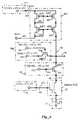
- FIG. 5Ashows the biasing conditions during programming of a memory cell 45 and FIG. 5B shows the biasing conditions during verifying and reading of the memory cell 45 .
- FIG. 5 A and FIG. 5Balso show the same circuit embodiment of some of the blocks shown previously in FIG. 4 .
- the memory cell 45programs with hot electrons generated in the middle of the channel using an HESSCHEI cell design.
- the common-line voltage control circuit block 41provides a high voltage VCL on the CL line 42 that is in the range of 6V to 12V during programming and voltage in the range of 2V to 6V during verifying or reading.
- the specific voltage applied on the CL line 42depends on the characteristics of the memory cell 45 .
- the control-gate voltage control circuit block 44provides a low voltage VCG on the CG line 43 that is in the range of 1V to 2V during programming and a voltage in the range of 2V to 6V during verifying and reading.
- the specific voltage applied on the CG line 43depends on the characteristics of the memory cell 45 .
- the bitline selection circuit block 46consists of an n-channel MOS. transistor MN 1 503 whose gate is connected to a voltage source VBLSEL 502 by a line 501 .
- the VBLSEL voltage source 502is controlled by the erase, program, verify & read circuit block 414 shown previously in FIG. 4 .
- the MN 1 transistor 503decouples the BL line 415 from the VR line 48 .
- the MN 1 transistor 503couples the BL line 415 to the VR line 48 .
- the pre-charge voltage control circuit block 404consists of an n-channel MOS transistor MN 2 506 , whose gate is connected to a voltage source VPCNTL by a line 505 .
- the VPCNTL voltage on the line 505is controlled by the erase, program, verify & read circuit block 414 shown previously in FIG. 4 .
- One end of the MN 2 transistor 506is connected to the VR line 48 and the other end is connected to a voltage source Vpchg through a line 504 .
- the Vpchg voltageis in the range of 0.5V to 2V during programming and in the range of 1V to 6V during verifying or reading.
- the specific voltage Vpchg useddepends on the characteristics of the memory cell 45 .
- the MN 2 transistor 506decouples the Vpchg voltage on line 504 from the VR line 48 .
- the transistor MN 2couples the Vpchg voltage on line 504 to the VR line 48 .
- the current control circuit block 403consists of a current mirror transistor pair consisting of n-channel MOS transistors MN 3 512 and MN 4 513 .
- the MN 3 transistor 512is in the diode; connected topology as understood by those skilled in the art.
- the diode connected side of the MN 3 transistor 512is connected to one side of a transistor MN 6 507 and a transistor MN 5 511 by a line 516 .
- the other end of the MN 3 transistor 512is connected the current end reference voltage circuit block 412 by the CERV line 408 .
- the gate of MN 4 transistor 513is connected to the gate of the MN 3 transistor 512 .
- One terminal of the MN 4 transistor 513is connected to the VR line 48 and the other terminal is connected to the current end reference voltage circuit block 412 by the CERV line 408 .
- the other end of the MN 6 transistor 507is connected to the IGEN line 407 .
- the gate of the MN 6 transistor 507is connected to a line 514 .
- the line 514is also connected to the output of a LATCH 510 and to the input of an INV inverter 509 .
- the output of the INV inverter 509is connected to the gate of the MN 5 transistor 511 by the line 515 .
- the other end of the MN 5 transistor 511is connected to the current end reference voltage circuit block 412 through the CERV line 408 .
- the input of the LATCH 510is connected to the logic output line 402 .
- IPULSEhas a magnitude in the range of 0.5 uA to 50 uA and a duration in the range of 1 usec to 10 usec, as shown in FIG. 5 A.
- ICONSTa constant current ICONST is applied to the IGEN line 407 by the bitline current generation block 411 , in shown previously in FIG. 4 .
- ICONSThas a magnitude in the range of 0.5 uA to 10 uA as shown in FIG. 5 B.
- the specific magnitude and duration used for IPULSE and magnitude used for ICONSTdepends on the characteristics of the memory cell 45 .
- the diode-connected side of the MN 3 transistor 512is coupled to the IPULSE current pulse source on the IGEN line 407 and the other side of the MN 3 transistor is coupled to 0V (ground) by the current end reference voltage circuit block 412 .
- the diode-connected side of the MN 3 transistor 512is coupled to the constant current source ICONST on the IGEN line 407 .
- the MN 4 transistor 513sinks a similar current pulse to 0V ground.
- the MN 4 transistor 513sinks a similar constant current to 0V ground.
- 0V groundis developed on the CERV line 408 by the current end reference voltage circuit block 412 .
- the current pulse IPULSE and the constant current ICONSTrespectively, pass through the MN 1 transistor 503 , through the memory cell 45 and are sourced by the voltage source VCL provided by the common-line voltage control circuit block 41 on the CL line 42 .
- the memory cell 45is erased.
- 0Vis applied on the CL line 42 by the VCL voltage source in the common-line voltage control circuit block 41
- 0Vis applied on the VR line 48 by the pre-charge voltage control circuit block 404
- 5Vis applied to the line 501 to couple the BL line 415 to the VR line 48
- the LATCH 510 in the current control circuit block 403is reset by the erase, program, verify and read control circuit block 414 shown previously in FIG. 4 .
- a high voltage pulse of magnitude 12V and 10 msec durationis applied on the CG line 43 by the VCG voltage source in the control-gate voltage control circuit block 44 .
- an erase verify cycleis performed.
- 4Vis applied on the CL line 42 and the CG line 43
- 5Vis applied to line 501 to couple the BL line 415 to the VR line 48
- a pre-charge voltage Vpchg of 4Vis applied to the VR line 48 to pre-charge the BL line 415 to 4V.
- a constant current ICONST of magnitude 10 uAis applied on the IGEN line 407 by the bitline current generation block 411
- 0Vground
- a reference voltage representing the erase levelis applied to the VREF line 401 , which is selected by the reference voltage selection circuit block 405 from the voltage bus RVGEN 409 .
- the reference voltages on the RVGEN voltage bus 409are generated by the reference voltage generation block 413 .
- the pre-charge voltageis next removed from the VR line 48 by applying 0V on line 505 in the bit line control circuit block 404 .
- the LATCH 510 in the current control circuit block 403is set by the erase, program, verify & read circuit block 414 .
- the constant current ICONSTpasses through the memory cell 45 and is sunk to 0V ground by the MN 4 transistor 513 .
- a stable voltageis developed on the VR line 48 .
- the voltage comparator 49is strobed to compare the voltage on the VR line 48 and the reference voltage on the VREF line 401 .
- the output of the comparator logic output 402is at a logic high level to signify that the memory cell 45 has been properly erased. Otherwise, the memory cell 45 goes through further erase and erase verify cycles.
- the voltages VCL, VCG, Vpchg, the constant current ICONST and the timing relationship during the erase verify cycleare the same as those applied during the program verify or read cycles. The difference is the application of an appropriate reference voltage on the VREF line 401 during the erase verify, the program verify and the read cycle.
- a high voltage 12Vis applied on the CL line 42 by the VCL voltage source in the common-line voltage control circuit block 41
- 2Vis applied on the VR line 48 by the pre-charge voltage control circuit block 404
- 5Vis applied to the line 501 to couple the BL line 415 to the VR line 48
- 0Vground
- the LATCH 510 in the current control circuit block 403is reset by the erase, program, verify & read control circuit block 414 .
- 2Vis applied on the CG line 43 by the VCG voltage source in the control-gate voltage control circuit block 44 .
- the LATCH 510 in the current control circuit block 403is set by the erase, program, verify & read circuit block 414 .
- a current pulse IPULSE starting at a low magnitude and a duration of 1 usecis applied on the IGEN line 407 by the bitline current generation block 411 .
- the pulse current IPULSEpasses through the memory cell 45 and is sunk to 0V ground by the MN 4 transistor 513 .
- the LATCH 510 in the current control circuit block 403is reset by the erase, program , verify & read circuit block 414 and no more current is sunk through the memory cell 45 .
- a program verification cycleis performed, exactly the same as that of the erase verification cycle.
- a reference voltage representing the desired program levelis applied to the VREF line 401 , which is selected by the reference voltage selection circuit block 405 from the voltage bus RVGEN 409 . If the logic output 402 of the comparator is low, the LATCH 514 is reset and no further programming current pulses are applied to the memory cell 45 . Otherwise, further program/verify cycles are performed on the memory cell 45 , until the logic output 402 of the comparator is low during a program verify cycle or an error flag is set in the erase, program, verify & read block 414 once a maximum number of program/verify cycles is reached. During each successive program cycle, the current pulse IPULSE is incremented by a certain amount dependent on the characteristics of the memory cell 45 .
- the current control circuit block 403 , the current end reference voltage circuit block 412 , the logic output line 402 , the CERV line 408 , and the IGEN line 407 all of which are part of the bitline driver 416do not require the use of high voltage circuitry which reduces circuit complexity.
- the use of voltage-mode sensingallows exactly the same circuit topology to be used for programming as for sensing operations further simplifying the circuit complexity.
- FIG. 6shows details of another embodiment during programming.
- current in sourced by the current control circuit block 403.
- the current control circuit block 403consists of a cascode current mirror consisting of p-channel transistors MP 1 601 , MP 2 603 , MP 3 602 and MP 4 604 .
- the voltage provided by the current end reference voltage circuit block 412 on the CERV line 408is higher in magnitude than the voltage provided by the common-line voltage control circuit block 41 on the CL line 42 .
- the voltage on the CERV line 408is in the range of 8V to 14V and the voltage on the CL line 42 is 0V.
- the bitline selection circuit block 46 , the control-gate voltage control circuit block 44 and the pre-charge voltage control circuit block 404perform the same function as taught in the previous embodiment.
- FIG. 7shows the block diagram of a memory array 715 consisting of M columns and N rows of memory cells 45 .
- a plurality of memory cells 45 from a selected rowcan be programmed in a paged-mode fashion to reduce the effective programming time.
- one of a selected X-Decode blocks 701 - 702select the appropriate pair of common-line voltage control circuit block 41 and control-gate voltage control circuit block 44 .
- Each selected X-Decode block 701 - 702thus selects the application of the appropriate voltages on a pair of lines CL and CG.
- X-Decode 702will select a pair of common-line voltage control circuit block 41 and control-gate voltage control circuit block 44 to allow the application of voltages on a CLN line 708 and a CGN line 709 . This way all the memory cells 45 in row number N have voltages applied.
- a Y-Decode block 705selects a page consisting of a plurality of columns, or bit lines, through the bitline selection circuit blocks 46 .
- each bitline selection circuit block 46is connected to only one bit line. It should be understood that the bitline selection circuits blocks 46 can be implemented to connect to a plurality of bit lines.
- a page of memory cells 45are programmed and verified in a parallel fashion.
- a pagecan be all, or a subset of, the memory cells 45 on a selected row.
- a read cyclea page of memory cells are read in parallel.
Landscapes
- Engineering & Computer Science (AREA)
- Computer Hardware Design (AREA)
- Microelectronics & Electronic Packaging (AREA)
- Read Only Memory (AREA)
Abstract
Description
Claims (42)
Priority Applications (2)
| Application Number | Priority Date | Filing Date | Title |
|---|---|---|---|
| US09/523,828US6285598B1 (en) | 1997-03-06 | 2000-03-13 | Precision programming of nonvolatile memory cells |
| US09/909,817US6487116B2 (en) | 1997-03-06 | 2001-07-20 | Precision programming of nonvolatile memory cells |
Applications Claiming Priority (3)
| Application Number | Priority Date | Filing Date | Title |
|---|---|---|---|
| US08/812,868US5870335A (en) | 1997-03-06 | 1997-03-06 | Precision programming of nonvolatile memory cells |
| US09/197,479US6038174A (en) | 1997-03-06 | 1998-11-20 | Precision programming of nonvolatile memory cells |
| US09/523,828US6285598B1 (en) | 1997-03-06 | 2000-03-13 | Precision programming of nonvolatile memory cells |
Related Parent Applications (1)
| Application Number | Title | Priority Date | Filing Date |
|---|---|---|---|
| US09/197,479ContinuationUS6038174A (en) | 1997-03-06 | 1998-11-20 | Precision programming of nonvolatile memory cells |
Related Child Applications (1)
| Application Number | Title | Priority Date | Filing Date |
|---|---|---|---|
| US09/909,817DivisionUS6487116B2 (en) | 1997-03-06 | 2001-07-20 | Precision programming of nonvolatile memory cells |
Publications (1)
| Publication Number | Publication Date |
|---|---|
| US6285598B1true US6285598B1 (en) | 2001-09-04 |
Family
ID=25210829
Family Applications (3)
| Application Number | Title | Priority Date | Filing Date |
|---|---|---|---|
| US08/812,868Expired - LifetimeUS5870335A (en) | 1997-03-06 | 1997-03-06 | Precision programming of nonvolatile memory cells |
| US09/197,479Expired - LifetimeUS6038174A (en) | 1997-03-06 | 1998-11-20 | Precision programming of nonvolatile memory cells |
| US09/523,828Expired - LifetimeUS6285598B1 (en) | 1997-03-06 | 2000-03-13 | Precision programming of nonvolatile memory cells |
Family Applications Before (2)
| Application Number | Title | Priority Date | Filing Date |
|---|---|---|---|
| US08/812,868Expired - LifetimeUS5870335A (en) | 1997-03-06 | 1997-03-06 | Precision programming of nonvolatile memory cells |
| US09/197,479Expired - LifetimeUS6038174A (en) | 1997-03-06 | 1998-11-20 | Precision programming of nonvolatile memory cells |
Country Status (6)
| Country | Link |
|---|---|
| US (3) | US5870335A (en) |
| EP (1) | EP0965132A4 (en) |
| JP (2) | JP2001501013A (en) |
| KR (1) | KR100697492B1 (en) |
| CN (1) | CN1169159C (en) |
| WO (1) | WO1998039775A1 (en) |
Cited By (11)
| Publication number | Priority date | Publication date | Assignee | Title |
|---|---|---|---|---|
| US20030135689A1 (en)* | 2002-01-17 | 2003-07-17 | Macronix International Co., Ltd. | Method of programming and erasing multi-level flash memory |
| US20040156241A1 (en)* | 2003-02-06 | 2004-08-12 | Nima Mokhlesi | System and method for programming cells in non-volatile integrated memory devices |
| US20040190340A1 (en)* | 2003-03-26 | 2004-09-30 | Yue-Der Chih | Word-line voltage generator |
| US20060291285A1 (en)* | 2003-02-06 | 2006-12-28 | Nima Mokhlesi | System and method for programming cells in non-volatile integrated memory devices |
| US20080049495A1 (en)* | 2006-08-28 | 2008-02-28 | Shigekazu Yamada | Method, apparatus and system relating to automatic cell threshold voltage measurement |
| US20090116290A1 (en)* | 2006-08-25 | 2009-05-07 | Micron Technology, Inc. | Methods and apparatuses relating to automatic cell threshold voltage measurement |
| US20090213643A1 (en)* | 2008-02-26 | 2009-08-27 | Michael Angerbauer | Integrated Circuit and Method of Improved Determining a Memory State of a Memory Cell |
| US7656710B1 (en) | 2005-07-14 | 2010-02-02 | Sau Ching Wong | Adaptive operations for nonvolatile memories |
| US20100125429A1 (en)* | 2008-11-14 | 2010-05-20 | Micron Technology, Inc. | Automatic word line leakage measurement circuitry |
| US8588007B2 (en) | 2011-02-28 | 2013-11-19 | Micron Technology, Inc. | Leakage measurement systems |
| US8634264B2 (en) | 2011-10-26 | 2014-01-21 | Micron Technology, Inc. | Apparatuses, integrated circuits, and methods for measuring leakage current |
Families Citing this family (95)
| Publication number | Priority date | Publication date | Assignee | Title |
|---|---|---|---|---|
| US6331724B1 (en)* | 1995-11-17 | 2001-12-18 | Nippon Precision Circuits, Inc. | Single transistor E2prom memory device with controlled erasing |
| IL125604A (en) | 1997-07-30 | 2004-03-28 | Saifun Semiconductors Ltd | Non-volatile electrically erasable and programmble semiconductor memory cell utilizing asymmetrical charge |
| US6768165B1 (en) | 1997-08-01 | 2004-07-27 | Saifun Semiconductors Ltd. | Two bit non-volatile electrically erasable and programmable semiconductor memory cell utilizing asymmetrical charge trapping |
| US6633496B2 (en) | 1997-12-12 | 2003-10-14 | Saifun Semiconductors Ltd. | Symmetric architecture for memory cells having widely spread metal bit lines |
| US6633499B1 (en) | 1997-12-12 | 2003-10-14 | Saifun Semiconductors Ltd. | Method for reducing voltage drops in symmetric array architectures |
| US6430077B1 (en) | 1997-12-12 | 2002-08-06 | Saifun Semiconductors Ltd. | Method for regulating read voltage level at the drain of a cell in a symmetric array |
| US6058042A (en)* | 1997-12-26 | 2000-05-02 | Sony Corporation | Semiconductor nonvolatile memory device and method of data programming the same |
| US6348711B1 (en) | 1998-05-20 | 2002-02-19 | Saifun Semiconductors Ltd. | NROM cell with self-aligned programming and erasure areas |
| US6215148B1 (en) | 1998-05-20 | 2001-04-10 | Saifun Semiconductors Ltd. | NROM cell with improved programming, erasing and cycling |
| US6346427B1 (en) | 1999-08-18 | 2002-02-12 | Utmc Microelectronic Systems Inc. | Parameter adjustment in a MOS integrated circuit |
| US6275415B1 (en)* | 1999-10-12 | 2001-08-14 | Advanced Micro Devices, Inc. | Multiple byte channel hot electron programming using ramped gate and source bias voltage |
| US6429063B1 (en) | 1999-10-26 | 2002-08-06 | Saifun Semiconductors Ltd. | NROM cell with generally decoupled primary and secondary injection |
| US6490204B2 (en) | 2000-05-04 | 2002-12-03 | Saifun Semiconductors Ltd. | Programming and erasing methods for a reference cell of an NROM array |
| US6928001B2 (en)* | 2000-12-07 | 2005-08-09 | Saifun Semiconductors Ltd. | Programming and erasing methods for a non-volatile memory cell |
| US6396741B1 (en)* | 2000-05-04 | 2002-05-28 | Saifun Semiconductors Ltd. | Programming of nonvolatile memory cells |
| US6292394B1 (en) | 2000-06-29 | 2001-09-18 | Saifun Semiconductors Ltd. | Method for programming of a semiconductor memory cell |
| US6396742B1 (en)* | 2000-07-28 | 2002-05-28 | Silicon Storage Technology, Inc. | Testing of multilevel semiconductor memory |
| US6614692B2 (en)* | 2001-01-18 | 2003-09-02 | Saifun Semiconductors Ltd. | EEPROM array and method for operation thereof |
| US6677805B2 (en)* | 2001-04-05 | 2004-01-13 | Saifun Semiconductors Ltd. | Charge pump stage with body effect minimization |
| US6584017B2 (en) | 2001-04-05 | 2003-06-24 | Saifun Semiconductors Ltd. | Method for programming a reference cell |
| US6636440B2 (en) | 2001-04-25 | 2003-10-21 | Saifun Semiconductors Ltd. | Method for operation of an EEPROM array, including refresh thereof |
| JP2002334588A (en)* | 2001-05-11 | 2002-11-22 | Seiko Epson Corp | Program method for nonvolatile semiconductor memory device |
| US6643181B2 (en) | 2001-10-24 | 2003-11-04 | Saifun Semiconductors Ltd. | Method for erasing a memory cell |
| US7098107B2 (en)* | 2001-11-19 | 2006-08-29 | Saifun Semiconductor Ltd. | Protective layer in memory device and method therefor |
| US6885585B2 (en)* | 2001-12-20 | 2005-04-26 | Saifun Semiconductors Ltd. | NROM NOR array |
| US6583007B1 (en) | 2001-12-20 | 2003-06-24 | Saifun Semiconductors Ltd. | Reducing secondary injection effects |
| KR20040071322A (en)* | 2002-01-16 | 2004-08-11 | 어드밴스드 마이크로 디바이시즈, 인코포레이티드 | Charge injection |
| US6700818B2 (en)* | 2002-01-31 | 2004-03-02 | Saifun Semiconductors Ltd. | Method for operating a memory device |
| US7190620B2 (en)* | 2002-01-31 | 2007-03-13 | Saifun Semiconductors Ltd. | Method for operating a memory device |
| JP4156248B2 (en)* | 2002-02-18 | 2008-09-24 | 株式会社ルネサステクノロジ | Nonvolatile semiconductor memory device |
| US6917544B2 (en)* | 2002-07-10 | 2005-07-12 | Saifun Semiconductors Ltd. | Multiple use memory chip |
| US6826107B2 (en)* | 2002-08-01 | 2004-11-30 | Saifun Semiconductors Ltd. | High voltage insertion in flash memory cards |
| US7136304B2 (en) | 2002-10-29 | 2006-11-14 | Saifun Semiconductor Ltd | Method, system and circuit for programming a non-volatile memory array |
| US6754103B2 (en)* | 2002-11-04 | 2004-06-22 | Silicon Storage Technology, Inc. | Method and apparatus for programming and testing a non-volatile memory cell for storing multibit states |
| US6967896B2 (en)* | 2003-01-30 | 2005-11-22 | Saifun Semiconductors Ltd | Address scramble |
| US7178004B2 (en)* | 2003-01-31 | 2007-02-13 | Yan Polansky | Memory array programming circuit and a method for using the circuit |
| US7142464B2 (en) | 2003-04-29 | 2006-11-28 | Saifun Semiconductors Ltd. | Apparatus and methods for multi-level sensing in a memory array |
| US6898128B2 (en)* | 2003-07-18 | 2005-05-24 | Freescale Semiconductor, Inc. | Programming of a memory with discrete charge storage elements |
| KR100505707B1 (en)* | 2003-08-26 | 2005-08-03 | 삼성전자주식회사 | Program control circuit of flash memory device for adjusting variable voltage level of bit line in program operation and control method of the same |
| US7123532B2 (en)* | 2003-09-16 | 2006-10-17 | Saifun Semiconductors Ltd. | Operating array cells with matched reference cells |
| US6956770B2 (en)* | 2003-09-17 | 2005-10-18 | Sandisk Corporation | Non-volatile memory and method with bit line compensation dependent on neighboring operating modes |
| JP2005129151A (en)* | 2003-10-23 | 2005-05-19 | Fujitsu Ltd | Semiconductor memory device |
| TWI247311B (en)* | 2004-03-25 | 2006-01-11 | Elite Semiconductor Esmt | Circuit and method for preventing nonvolatile memory from over erasure |
| WO2005094178A2 (en)* | 2004-04-01 | 2005-10-13 | Saifun Semiconductors Ltd. | Method, circuit and systems for erasing one or more non-volatile memory cells |
| US7490283B2 (en) | 2004-05-13 | 2009-02-10 | Sandisk Corporation | Pipelined data relocation and improved chip architectures |
| US7366025B2 (en)* | 2004-06-10 | 2008-04-29 | Saifun Semiconductors Ltd. | Reduced power programming of non-volatile cells |
| US7317633B2 (en) | 2004-07-06 | 2008-01-08 | Saifun Semiconductors Ltd | Protection of NROM devices from charge damage |
| WO2006011222A1 (en)* | 2004-07-30 | 2006-02-02 | Spansion Llc | Semiconductor device and writing method |
| US7095655B2 (en)* | 2004-08-12 | 2006-08-22 | Saifun Semiconductors Ltd. | Dynamic matching of signal path and reference path for sensing |
| US20060036803A1 (en)* | 2004-08-16 | 2006-02-16 | Mori Edan | Non-volatile memory device controlled by a micro-controller |
| US20060068551A1 (en)* | 2004-09-27 | 2006-03-30 | Saifun Semiconductors, Ltd. | Method for embedding NROM |
| US7638850B2 (en)* | 2004-10-14 | 2009-12-29 | Saifun Semiconductors Ltd. | Non-volatile memory structure and method of fabrication |
| US20060146624A1 (en)* | 2004-12-02 | 2006-07-06 | Saifun Semiconductors, Ltd. | Current folding sense amplifier |
| US7535765B2 (en) | 2004-12-09 | 2009-05-19 | Saifun Semiconductors Ltd. | Non-volatile memory device and method for reading cells |
| US7120051B2 (en)* | 2004-12-14 | 2006-10-10 | Sandisk Corporation | Pipelined programming of non-volatile memories using early data |
| US7420847B2 (en)* | 2004-12-14 | 2008-09-02 | Sandisk Corporation | Multi-state memory having data recovery after program fail |
| US7158421B2 (en)* | 2005-04-01 | 2007-01-02 | Sandisk Corporation | Use of data latches in multi-phase programming of non-volatile memories |
| US7849381B2 (en)* | 2004-12-21 | 2010-12-07 | Sandisk Corporation | Method for copying data in reprogrammable non-volatile memory |
| US7130210B2 (en)* | 2005-01-13 | 2006-10-31 | Spansion Llc | Multi-level ONO flash program algorithm for threshold width control |
| EP1686592A3 (en)* | 2005-01-19 | 2007-04-25 | Saifun Semiconductors Ltd. | Partial erase verify |
| US7212939B2 (en)* | 2005-02-18 | 2007-05-01 | Taiwan Semiconductor Manufacturin Co., Ltd. | Method and system for timing measurement of embedded macro module |
| US8053812B2 (en) | 2005-03-17 | 2011-11-08 | Spansion Israel Ltd | Contact in planar NROM technology |
| US7463521B2 (en) | 2005-04-01 | 2008-12-09 | Sandisk Corporation | Method for non-volatile memory with managed execution of cached data |
| US7447078B2 (en)* | 2005-04-01 | 2008-11-04 | Sandisk Corporation | Method for non-volatile memory with background data latch caching during read operations |
| US7206230B2 (en)* | 2005-04-01 | 2007-04-17 | Sandisk Corporation | Use of data latches in cache operations of non-volatile memories |
| US20070141788A1 (en)* | 2005-05-25 | 2007-06-21 | Ilan Bloom | Method for embedding non-volatile memory with logic circuitry |
| US8400841B2 (en)* | 2005-06-15 | 2013-03-19 | Spansion Israel Ltd. | Device to program adjacent storage cells of different NROM cells |
| US7184313B2 (en)* | 2005-06-17 | 2007-02-27 | Saifun Semiconductors Ltd. | Method circuit and system for compensating for temperature induced margin loss in non-volatile memory cells |
| US7786512B2 (en)* | 2005-07-18 | 2010-08-31 | Saifun Semiconductors Ltd. | Dense non-volatile memory array and method of fabrication |
| US20070036007A1 (en)* | 2005-08-09 | 2007-02-15 | Saifun Semiconductors, Ltd. | Sticky bit buffer |
| US7668017B2 (en) | 2005-08-17 | 2010-02-23 | Saifun Semiconductors Ltd. | Method of erasing non-volatile memory cells |
| US20070096199A1 (en)* | 2005-09-08 | 2007-05-03 | Eli Lusky | Method of manufacturing symmetric arrays |
| US7221138B2 (en) | 2005-09-27 | 2007-05-22 | Saifun Semiconductors Ltd | Method and apparatus for measuring charge pump output current |
| US20070120180A1 (en)* | 2005-11-25 | 2007-05-31 | Boaz Eitan | Transition areas for dense memory arrays |
| US7352627B2 (en)* | 2006-01-03 | 2008-04-01 | Saifon Semiconductors Ltd. | Method, system, and circuit for operating a non-volatile memory array |
| US7808818B2 (en)* | 2006-01-12 | 2010-10-05 | Saifun Semiconductors Ltd. | Secondary injection for NROM |
| US20070173017A1 (en)* | 2006-01-20 | 2007-07-26 | Saifun Semiconductors, Ltd. | Advanced non-volatile memory array and method of fabrication thereof |
| US7692961B2 (en)* | 2006-02-21 | 2010-04-06 | Saifun Semiconductors Ltd. | Method, circuit and device for disturb-control of programming nonvolatile memory cells by hot-hole injection (HHI) and by channel hot-electron (CHE) injection |
| US7760554B2 (en)* | 2006-02-21 | 2010-07-20 | Saifun Semiconductors Ltd. | NROM non-volatile memory and mode of operation |
| US8253452B2 (en)* | 2006-02-21 | 2012-08-28 | Spansion Israel Ltd | Circuit and method for powering up an integrated circuit and an integrated circuit utilizing same |
| US7638835B2 (en) | 2006-02-28 | 2009-12-29 | Saifun Semiconductors Ltd. | Double density NROM with nitride strips (DDNS) |
| US8077521B2 (en)* | 2006-03-16 | 2011-12-13 | Freescale Semiconductor, Inc. | Bitline current generator for a non-volatile memory array and a non-volatile memory array |
| US20070255889A1 (en)* | 2006-03-22 | 2007-11-01 | Yoav Yogev | Non-volatile memory device and method of operating the device |
| US7701779B2 (en)* | 2006-04-27 | 2010-04-20 | Sajfun Semiconductors Ltd. | Method for programming a reference cell |
| KR101020812B1 (en)* | 2006-06-19 | 2011-03-09 | 샌디스크 코포레이션 | Sense and different sized margin programming with compensation on select for improved read operation in nonvolatile memory |
| US7605579B2 (en)* | 2006-09-18 | 2009-10-20 | Saifun Semiconductors Ltd. | Measuring and controlling current consumption and output current of charge pumps |
| US20080239599A1 (en)* | 2007-04-01 | 2008-10-02 | Yehuda Yizraeli | Clamping Voltage Events Such As ESD |
| KR20090010481A (en)* | 2007-07-23 | 2009-01-30 | 삼성전자주식회사 | NAND flash memory device, and its programming method to program optional transistors |
| US7590001B2 (en) | 2007-12-18 | 2009-09-15 | Saifun Semiconductors Ltd. | Flash memory with optimized write sector spares |
| JP5127439B2 (en)* | 2007-12-28 | 2013-01-23 | 株式会社東芝 | Semiconductor memory device |
| JP2010079977A (en)* | 2008-09-25 | 2010-04-08 | Toppan Printing Co Ltd | Nonvolatile semiconductor memory device with constant current type power supply circuit |
| US8472280B2 (en) | 2010-12-21 | 2013-06-25 | Sandisk Technologies Inc. | Alternate page by page programming scheme |
| KR20150073487A (en)* | 2013-12-23 | 2015-07-01 | 에스케이하이닉스 주식회사 | Semiconductor Memory Apparatus |
| CN106158030B (en)* | 2015-04-28 | 2019-09-24 | 旺宏电子股份有限公司 | Method of programming a memory device and related memory device |
| CN114400041A (en)* | 2021-03-15 | 2022-04-26 | 长江存储科技有限责任公司 | Verification error bit quantization circuit and method for semiconductor memory |
Citations (83)
| Publication number | Priority date | Publication date | Assignee | Title |
|---|---|---|---|---|
| US4054864A (en) | 1973-05-04 | 1977-10-18 | Commissariat A L'energie Atomique | Method and device for the storage of analog signals |
| US4181980A (en) | 1978-05-15 | 1980-01-01 | Electronic Arrays, Inc. | Acquisition and storage of analog signals |
| US4415992A (en) | 1981-02-25 | 1983-11-15 | Motorola, Inc. | Memory system having memory cells capable of storing more than two states |
| US4448400A (en) | 1981-07-13 | 1984-05-15 | Eliyahou Harari | Highly scalable dynamic RAM cell with self-signal amplification |
| US4612629A (en) | 1981-07-13 | 1986-09-16 | Eliyahou Harari | Highly scalable dynamic RAM cell with self-signal amplification |
| US4622656A (en) | 1982-12-16 | 1986-11-11 | Seiko Instruments & Electronics Ltd. | Non-volatile semiconductor memory |
| US4627027A (en) | 1982-09-01 | 1986-12-02 | Sanyo Electric Co., Ltd. | Analog storing and reproducing apparatus utilizing non-volatile memory elements |
| US4667217A (en) | 1985-04-19 | 1987-05-19 | Ncr Corporation | Two bit vertically/horizontally integrated memory cell |
| US4771404A (en) | 1984-09-05 | 1988-09-13 | Nippon Telegraph And Telephone Corporation | Memory device employing multilevel storage circuits |
| US4794565A (en) | 1986-09-15 | 1988-12-27 | The Regents Of The University Of California | Electrically programmable memory device employing source side injection |
| US4890259A (en) | 1988-07-13 | 1989-12-26 | Information Storage Devices | High density integrated circuit analog signal recording and playback system |
| WO1990012400A1 (en) | 1989-04-13 | 1990-10-18 | Sundisk Corporation | Multi-state eeprom read and write circuits and techniques |
| US4989179A (en) | 1988-07-13 | 1991-01-29 | Information Storage Devices, Inc. | High density integrated circuit analog signal recording and playback system |
| US5029130A (en) | 1990-01-22 | 1991-07-02 | Silicon Storage Technology, Inc. | Single transistor non-valatile electrically alterable semiconductor memory device |
| US5042009A (en) | 1988-12-09 | 1991-08-20 | Waferscale Integration, Inc. | Method for programming a floating gate memory device |
| US5043940A (en) | 1988-06-08 | 1991-08-27 | Eliyahou Harari | Flash EEPROM memory systems having multistate storage cells |
| US5119330A (en) | 1989-03-31 | 1992-06-02 | Oki Electric Industry Co, Ltd. | Nonvolatile memory system for multiple value storing |
| US5150327A (en) | 1988-10-31 | 1992-09-22 | Matsushita Electric Industrial Co., Ltd. | Semiconductor memory and video signal processing circuit having the same |
| US5198380A (en) | 1988-06-08 | 1993-03-30 | Sundisk Corporation | Method of highly compact EPROM and flash EEPROM devices |
| US5218569A (en) | 1991-02-08 | 1993-06-08 | Banks Gerald J | Electrically alterable non-volatile memory with n-bits per memory cell |
| US5218571A (en) | 1990-05-07 | 1993-06-08 | Cypress Semiconductor Corporation | EPROM source bias circuit with compensation for processing characteristics |
| US5220531A (en) | 1991-01-02 | 1993-06-15 | Information Storage Devices, Inc. | Source follower storage cell and improved method and apparatus for iterative write for integrated circuit analog signal recording and playback |
| US5222047A (en) | 1987-05-15 | 1993-06-22 | Mitsubishi Denki Kabushiki Kaisha | Method and apparatus for driving word line in block access memory |
| US5241494A (en) | 1990-09-26 | 1993-08-31 | Information Storage Devices | Integrated circuit system for analog signal recording and playback |
| US5243239A (en) | 1991-01-22 | 1993-09-07 | Information Storage Devices, Inc. | Integrated MOSFET resistance and oscillator frequency control and trim methods and apparatus |
| US5258759A (en) | 1992-10-16 | 1993-11-02 | California Institute Of Technology | Method and apparatus for monotonic algorithmic digital-to-analog and analog-to-digital conversion |
| US5258949A (en) | 1990-12-03 | 1993-11-02 | Motorola, Inc. | Nonvolatile memory with enhanced carrier generation and method for programming the same |
| US5268870A (en) | 1988-06-08 | 1993-12-07 | Eliyahou Harari | Flash EEPROM system and intelligent programming and erasing methods therefor |
| US5283761A (en) | 1992-07-22 | 1994-02-01 | Mosaid Technologies Incorporated | Method of multi-level storage in DRAM |
| US5293560A (en) | 1988-06-08 | 1994-03-08 | Eliyahou Harari | Multi-state flash EEPROM system using incremental programing and erasing methods |
| US5294819A (en) | 1992-11-25 | 1994-03-15 | Information Storage Devices | Single-transistor cell EEPROM array for analog or digital storage |
| US5297096A (en) | 1990-06-15 | 1994-03-22 | Mitsubishi Denki Kabushiki Kaisha | Nonvolatile semiconductor memory device and data erasing method thereof |
| US5313421A (en) | 1992-01-14 | 1994-05-17 | Sundisk Corporation | EEPROM with split gate source side injection |
| US5336936A (en) | 1992-05-06 | 1994-08-09 | Synaptics, Incorporated | One-transistor adaptable analog storage element and array |
| US5357476A (en) | 1993-06-01 | 1994-10-18 | Motorola, Inc. | Apparatus and method for erasing a flash EEPROM |
| US5365486A (en) | 1992-12-16 | 1994-11-15 | Texas Instruments Incorporated | Method and circuitry for refreshing a flash electrically erasable, programmable read only memory |
| US5371031A (en) | 1990-08-01 | 1994-12-06 | Texas Instruments Incorporated | Method of making EEPROM array with buried N+ windows and with separate erasing and programming regions |
| US5388064A (en) | 1991-11-26 | 1995-02-07 | Information Storage Devices, Inc. | Programmable non-volatile analog voltage source devices and methods |
| US5412601A (en) | 1992-08-31 | 1995-05-02 | Nippon Steel Corporation | Non-volatile semiconductor memory device capable of storing multi-value data in each memory cell |
| US5422842A (en) | 1993-07-08 | 1995-06-06 | Sundisk Corporation | Method and circuit for simultaneously programming and verifying the programming of selected EEPROM cells |
| WO1995020224A1 (en) | 1994-01-22 | 1995-07-27 | Memory Corporation Plc | Analogue memory system |
| US5440518A (en) | 1991-06-12 | 1995-08-08 | Hazani; Emanuel | Non-volatile memory circuits, architecture and methods |
| US5440505A (en) | 1994-01-21 | 1995-08-08 | Intel Corporation | Method and circuitry for storing discrete amounts of charge in a single memory element |
| US5475634A (en) | 1992-03-13 | 1995-12-12 | Silicon Storage Technology, Inc. | Floating gate memory array with latches having improved immunity to write disturbance, and with storage latches |
| US5477499A (en) | 1993-10-13 | 1995-12-19 | Advanced Micro Devices, Inc. | Memory architecture for a three volt flash EEPROM |
| US5479170A (en) | 1992-10-16 | 1995-12-26 | California Institute Of Technology | Method and apparatus for long-term multi-valued storage in dynamic analog memory |
| US5485422A (en) | 1994-06-02 | 1996-01-16 | Intel Corporation | Drain bias multiplexing for multiple bit flash cell |
| US5487033A (en) | 1994-06-28 | 1996-01-23 | Intel Corporation | Structure and method for low current programming of flash EEPROMS |
| WO1996004658A1 (en) | 1994-08-02 | 1996-02-15 | Memory Corporation Plc | Bit resolution optimising mechanism |
| US5508958A (en) | 1994-09-29 | 1996-04-16 | Intel Corporation | Method and apparatus for sensing the state of floating gate memory cells by applying a variable gate voltage |
| US5511020A (en) | 1993-11-23 | 1996-04-23 | Monolithic System Technology, Inc. | Pseudo-nonvolatile memory incorporating data refresh operation |
| US5521865A (en) | 1994-03-15 | 1996-05-28 | Kabushiki Kaisha Toshiba | Non-volatile semiconductor memory device for storing multi-value data |
| US5521878A (en) | 1993-09-13 | 1996-05-28 | Mitsubishi Denki Kabushiki Kaisha | Clock synchronous semiconductor memory device |
| US5523972A (en) | 1994-06-02 | 1996-06-04 | Intel Corporation | Method and apparatus for verifying the programming of multi-level flash EEPROM memory |
| US5539690A (en) | 1994-06-02 | 1996-07-23 | Intel Corporation | Write verify schemes for flash memory with multilevel cells |
| US5546341A (en) | 1993-01-13 | 1996-08-13 | Samsung Electronics Co., Ltd. | Nonvolatile semiconductor memory |
| US5555519A (en) | 1992-09-22 | 1996-09-10 | Kabushiki Kaisha Toshiba | Dynamic random access memory device with the combined open/folded bit-line pair arrangement |
| US5566111A (en) | 1995-09-18 | 1996-10-15 | Lg Semicon Co., Ltd. | Method for programming a nonvolatile memory |
| US5590076A (en) | 1995-06-21 | 1996-12-31 | Advanced Micro Devices, Inc. | Channel hot-carrier page write |
| US5592415A (en) | 1992-07-06 | 1997-01-07 | Hitachi, Ltd. | Non-volatile semiconductor memory |
| US5615163A (en) | 1993-12-21 | 1997-03-25 | Kabushiki Kaisha Toshiba | Semiconductor memory device |
| US5615159A (en) | 1995-11-28 | 1997-03-25 | Micron Quantum Devices, Inc. | Memory system with non-volatile data storage unit and method of initializing same |
| WO1997013250A1 (en) | 1995-10-06 | 1997-04-10 | Agate Semiconductor, Inc. | Integrated circuit for storage and retrieval of multiple digital bits per nonvolatile memory cell |
| US5627784A (en) | 1995-07-28 | 1997-05-06 | Micron Quantum Devices, Inc. | Memory system having non-volatile data storage structure for memory control parameters and method |
| US5629890A (en) | 1994-09-14 | 1997-05-13 | Information Storage Devices, Inc. | Integrated circuit system for analog signal storing and recovery incorporating read while writing voltage program method |
| US5633822A (en) | 1993-03-18 | 1997-05-27 | Sgs-Thomson Microelectronics S.R.L. | Method of programming a nonvolatile flash-EEPROM memory array using source line switching transistors |
| US5652450A (en) | 1995-08-11 | 1997-07-29 | Sharp Kabushiki Kaisha | Nonvolatile semiconductor storage device |
| US5657332A (en) | 1992-05-20 | 1997-08-12 | Sandisk Corporation | Soft errors handling in EEPROM devices |
| US5663923A (en) | 1995-04-28 | 1997-09-02 | Intel Corporation | Nonvolatile memory blocking architecture |
| US5671176A (en) | 1995-09-19 | 1997-09-23 | Samsung Electronics Co., Ltd. | Semiconductor memory device including program inhibition capacitors and method for controlling program-disturb of non-selected memory cells |
| US5694356A (en) | 1994-11-02 | 1997-12-02 | Invoice Technology, Inc. | High resolution analog storage EPROM and flash EPROM |
| US5708620A (en) | 1996-04-04 | 1998-01-13 | Lg Semicon Co., Ltd | Memory device having a plurality of bitlines between adjacent columns of sub-wordline drivers |
| US5712815A (en) | 1996-04-22 | 1998-01-27 | Advanced Micro Devices, Inc. | Multiple bits per-cell flash EEPROM capable of concurrently programming and verifying memory cells and reference cells |
| WO1998008337A1 (en) | 1996-08-21 | 1998-02-26 | Hitachi, Ltd. | Electronic camera with liquid crystal display |
| US5761117A (en) | 1995-08-31 | 1998-06-02 | Sanyo Electric Co., Ltd. | Non-volatile multi-state memory device with memory cell capable of storing multi-state data |
| US5761109A (en) | 1995-03-16 | 1998-06-02 | Kabushiki Kaisha Toshiba | Semiconductor memory device having folded bit line array and an open bit line array with imbalance correction |
| US5764586A (en) | 1996-10-10 | 1998-06-09 | Catalyst Semiconductor, Inc. | Intermediate size non-volatile electrically alterable semiconductor memory device |
| JPH10214494A (en) | 1997-01-31 | 1998-08-11 | Sony Corp | Non-volatile semiconductor memory |
| US5801989A (en) | 1995-12-11 | 1998-09-01 | Samsung Electronics, Co., Ltd. | Method and apparatus for optimizing erase and program times for a non-volatile memory device |
| EP0580467B1 (en) | 1992-07-24 | 1998-09-02 | SanDisk Corporation | Segmented column memory array |
| US5870332A (en)* | 1996-04-22 | 1999-02-09 | United Technologies Corporation | High reliability logic circuit for radiation environment |
| US5896340A (en) | 1997-07-07 | 1999-04-20 | Invox Technology | Multiple array architecture for analog or multi-bit-cell memory |
| US5969987A (en) | 1995-07-31 | 1999-10-19 | Information Storage Devices, Inc. | Non-volatile electrically alterable semiconductor memory for analog and digital storage |
Family Cites Families (2)
| Publication number | Priority date | Publication date | Assignee | Title |
|---|---|---|---|---|
| US5563823A (en)* | 1993-08-31 | 1996-10-08 | Macronix International Co., Ltd. | Fast FLASH EPROM programming and pre-programming circuit design |
| JP5491809B2 (en)* | 2009-09-25 | 2014-05-14 | パナソニック株式会社 | Grid-connected inverter device |
- 1997
- 1997-03-06USUS08/812,868patent/US5870335A/ennot_activeExpired - Lifetime
- 1998
- 1998-03-06CNCNB988031043Apatent/CN1169159C/ennot_activeExpired - Lifetime
- 1998-03-06EPEP98909036Apatent/EP0965132A4/ennot_activeWithdrawn
- 1998-03-06WOPCT/US1998/004511patent/WO1998039775A1/enactiveIP Right Grant
- 1998-03-06KRKR1019997008083Apatent/KR100697492B1/ennot_activeExpired - Lifetime
- 1998-03-06JPJP10538894Apatent/JP2001501013A/ennot_activeWithdrawn
- 1998-11-20USUS09/197,479patent/US6038174A/ennot_activeExpired - Lifetime
- 2000
- 2000-03-13USUS09/523,828patent/US6285598B1/ennot_activeExpired - Lifetime
- 2005
- 2005-11-24JPJP2005338253Apatent/JP4286251B2/ennot_activeExpired - Lifetime
Patent Citations (91)
| Publication number | Priority date | Publication date | Assignee | Title |
|---|---|---|---|---|
| US4054864A (en) | 1973-05-04 | 1977-10-18 | Commissariat A L'energie Atomique | Method and device for the storage of analog signals |
| US4181980A (en) | 1978-05-15 | 1980-01-01 | Electronic Arrays, Inc. | Acquisition and storage of analog signals |
| US4415992A (en) | 1981-02-25 | 1983-11-15 | Motorola, Inc. | Memory system having memory cells capable of storing more than two states |
| US4448400A (en) | 1981-07-13 | 1984-05-15 | Eliyahou Harari | Highly scalable dynamic RAM cell with self-signal amplification |
| US4612629A (en) | 1981-07-13 | 1986-09-16 | Eliyahou Harari | Highly scalable dynamic RAM cell with self-signal amplification |
| US4627027A (en) | 1982-09-01 | 1986-12-02 | Sanyo Electric Co., Ltd. | Analog storing and reproducing apparatus utilizing non-volatile memory elements |
| US4622656A (en) | 1982-12-16 | 1986-11-11 | Seiko Instruments & Electronics Ltd. | Non-volatile semiconductor memory |
| US4771404A (en) | 1984-09-05 | 1988-09-13 | Nippon Telegraph And Telephone Corporation | Memory device employing multilevel storage circuits |
| US4667217A (en) | 1985-04-19 | 1987-05-19 | Ncr Corporation | Two bit vertically/horizontally integrated memory cell |
| US4794565A (en) | 1986-09-15 | 1988-12-27 | The Regents Of The University Of California | Electrically programmable memory device employing source side injection |
| US5222047A (en) | 1987-05-15 | 1993-06-22 | Mitsubishi Denki Kabushiki Kaisha | Method and apparatus for driving word line in block access memory |
| US5198380A (en) | 1988-06-08 | 1993-03-30 | Sundisk Corporation | Method of highly compact EPROM and flash EEPROM devices |
| US5293560A (en) | 1988-06-08 | 1994-03-08 | Eliyahou Harari | Multi-state flash EEPROM system using incremental programing and erasing methods |
| US5268870A (en) | 1988-06-08 | 1993-12-07 | Eliyahou Harari | Flash EEPROM system and intelligent programming and erasing methods therefor |
| US5043940A (en) | 1988-06-08 | 1991-08-27 | Eliyahou Harari | Flash EEPROM memory systems having multistate storage cells |
| US4890259A (en) | 1988-07-13 | 1989-12-26 | Information Storage Devices | High density integrated circuit analog signal recording and playback system |
| US4989179A (en) | 1988-07-13 | 1991-01-29 | Information Storage Devices, Inc. | High density integrated circuit analog signal recording and playback system |
| US5150327A (en) | 1988-10-31 | 1992-09-22 | Matsushita Electric Industrial Co., Ltd. | Semiconductor memory and video signal processing circuit having the same |
| US5042009A (en) | 1988-12-09 | 1991-08-20 | Waferscale Integration, Inc. | Method for programming a floating gate memory device |
| US5119330A (en) | 1989-03-31 | 1992-06-02 | Oki Electric Industry Co, Ltd. | Nonvolatile memory system for multiple value storing |
| US5172338A (en) | 1989-04-13 | 1992-12-15 | Sundisk Corporation | Multi-state EEprom read and write circuits and techniques |
| US5172338B1 (en) | 1989-04-13 | 1997-07-08 | Sandisk Corp | Multi-state eeprom read and write circuits and techniques |
| WO1990012400A1 (en) | 1989-04-13 | 1990-10-18 | Sundisk Corporation | Multi-state eeprom read and write circuits and techniques |
| US5029130A (en) | 1990-01-22 | 1991-07-02 | Silicon Storage Technology, Inc. | Single transistor non-valatile electrically alterable semiconductor memory device |
| US5218571A (en) | 1990-05-07 | 1993-06-08 | Cypress Semiconductor Corporation | EPROM source bias circuit with compensation for processing characteristics |
| US5297096A (en) | 1990-06-15 | 1994-03-22 | Mitsubishi Denki Kabushiki Kaisha | Nonvolatile semiconductor memory device and data erasing method thereof |
| US5371031A (en) | 1990-08-01 | 1994-12-06 | Texas Instruments Incorporated | Method of making EEPROM array with buried N+ windows and with separate erasing and programming regions |
| US5241494A (en) | 1990-09-26 | 1993-08-31 | Information Storage Devices | Integrated circuit system for analog signal recording and playback |
| US5258949A (en) | 1990-12-03 | 1993-11-02 | Motorola, Inc. | Nonvolatile memory with enhanced carrier generation and method for programming the same |
| US5220531A (en) | 1991-01-02 | 1993-06-15 | Information Storage Devices, Inc. | Source follower storage cell and improved method and apparatus for iterative write for integrated circuit analog signal recording and playback |
| US5243239A (en) | 1991-01-22 | 1993-09-07 | Information Storage Devices, Inc. | Integrated MOSFET resistance and oscillator frequency control and trim methods and apparatus |
| US5352934A (en) | 1991-01-22 | 1994-10-04 | Information Storage Devices, Inc. | Integrated mosfet resistance and oscillator frequency control and trim methods and apparatus |
| US5218569A (en) | 1991-02-08 | 1993-06-08 | Banks Gerald J | Electrically alterable non-volatile memory with n-bits per memory cell |
| US5394362A (en) | 1991-02-08 | 1995-02-28 | Banks; Gerald J. | Electrically alterable non-voltatile memory with N-bits per memory cell |
| US5440518A (en) | 1991-06-12 | 1995-08-08 | Hazani; Emanuel | Non-volatile memory circuits, architecture and methods |
| US5388064A (en) | 1991-11-26 | 1995-02-07 | Information Storage Devices, Inc. | Programmable non-volatile analog voltage source devices and methods |
| US5313421A (en) | 1992-01-14 | 1994-05-17 | Sundisk Corporation | EEPROM with split gate source side injection |
| US5475634A (en) | 1992-03-13 | 1995-12-12 | Silicon Storage Technology, Inc. | Floating gate memory array with latches having improved immunity to write disturbance, and with storage latches |
| US5336936A (en) | 1992-05-06 | 1994-08-09 | Synaptics, Incorporated | One-transistor adaptable analog storage element and array |
| US5657332A (en) | 1992-05-20 | 1997-08-12 | Sandisk Corporation | Soft errors handling in EEPROM devices |
| US5592415A (en) | 1992-07-06 | 1997-01-07 | Hitachi, Ltd. | Non-volatile semiconductor memory |
| US5283761A (en) | 1992-07-22 | 1994-02-01 | Mosaid Technologies Incorporated | Method of multi-level storage in DRAM |
| EP0580467B1 (en) | 1992-07-24 | 1998-09-02 | SanDisk Corporation | Segmented column memory array |
| US5412601A (en) | 1992-08-31 | 1995-05-02 | Nippon Steel Corporation | Non-volatile semiconductor memory device capable of storing multi-value data in each memory cell |
| US5555519A (en) | 1992-09-22 | 1996-09-10 | Kabushiki Kaisha Toshiba | Dynamic random access memory device with the combined open/folded bit-line pair arrangement |
| US5479170A (en) | 1992-10-16 | 1995-12-26 | California Institute Of Technology | Method and apparatus for long-term multi-valued storage in dynamic analog memory |
| US5258759A (en) | 1992-10-16 | 1993-11-02 | California Institute Of Technology | Method and apparatus for monotonic algorithmic digital-to-analog and analog-to-digital conversion |
| US5294819A (en) | 1992-11-25 | 1994-03-15 | Information Storage Devices | Single-transistor cell EEPROM array for analog or digital storage |
| US5365486A (en) | 1992-12-16 | 1994-11-15 | Texas Instruments Incorporated | Method and circuitry for refreshing a flash electrically erasable, programmable read only memory |
| US5546341A (en) | 1993-01-13 | 1996-08-13 | Samsung Electronics Co., Ltd. | Nonvolatile semiconductor memory |
| US5633822A (en) | 1993-03-18 | 1997-05-27 | Sgs-Thomson Microelectronics S.R.L. | Method of programming a nonvolatile flash-EEPROM memory array using source line switching transistors |
| US5357476A (en) | 1993-06-01 | 1994-10-18 | Motorola, Inc. | Apparatus and method for erasing a flash EEPROM |
| US5422842A (en) | 1993-07-08 | 1995-06-06 | Sundisk Corporation | Method and circuit for simultaneously programming and verifying the programming of selected EEPROM cells |
| US5521878A (en) | 1993-09-13 | 1996-05-28 | Mitsubishi Denki Kabushiki Kaisha | Clock synchronous semiconductor memory device |
| US5477499A (en) | 1993-10-13 | 1995-12-19 | Advanced Micro Devices, Inc. | Memory architecture for a three volt flash EEPROM |
| US5511020A (en) | 1993-11-23 | 1996-04-23 | Monolithic System Technology, Inc. | Pseudo-nonvolatile memory incorporating data refresh operation |
| US5615163A (en) | 1993-12-21 | 1997-03-25 | Kabushiki Kaisha Toshiba | Semiconductor memory device |
| US5440505A (en) | 1994-01-21 | 1995-08-08 | Intel Corporation | Method and circuitry for storing discrete amounts of charge in a single memory element |
| US5566125A (en) | 1994-01-21 | 1996-10-15 | Intel Corporation | Method and circuitry for storing discrete amounts of charge in a single memory element |
| WO1995020224A1 (en) | 1994-01-22 | 1995-07-27 | Memory Corporation Plc | Analogue memory system |
| US5521865A (en) | 1994-03-15 | 1996-05-28 | Kabushiki Kaisha Toshiba | Non-volatile semiconductor memory device for storing multi-value data |
| US5523972A (en) | 1994-06-02 | 1996-06-04 | Intel Corporation | Method and apparatus for verifying the programming of multi-level flash EEPROM memory |
| US5539690A (en) | 1994-06-02 | 1996-07-23 | Intel Corporation | Write verify schemes for flash memory with multilevel cells |
| US5485422A (en) | 1994-06-02 | 1996-01-16 | Intel Corporation | Drain bias multiplexing for multiple bit flash cell |
| US5487033A (en) | 1994-06-28 | 1996-01-23 | Intel Corporation | Structure and method for low current programming of flash EEPROMS |
| WO1996004658A1 (en) | 1994-08-02 | 1996-02-15 | Memory Corporation Plc | Bit resolution optimising mechanism |
| US5629890A (en) | 1994-09-14 | 1997-05-13 | Information Storage Devices, Inc. | Integrated circuit system for analog signal storing and recovery incorporating read while writing voltage program method |
| US5508958A (en) | 1994-09-29 | 1996-04-16 | Intel Corporation | Method and apparatus for sensing the state of floating gate memory cells by applying a variable gate voltage |
| US5694356A (en) | 1994-11-02 | 1997-12-02 | Invoice Technology, Inc. | High resolution analog storage EPROM and flash EPROM |
| US5761109A (en) | 1995-03-16 | 1998-06-02 | Kabushiki Kaisha Toshiba | Semiconductor memory device having folded bit line array and an open bit line array with imbalance correction |
| US5663923A (en) | 1995-04-28 | 1997-09-02 | Intel Corporation | Nonvolatile memory blocking architecture |
| US5590076A (en) | 1995-06-21 | 1996-12-31 | Advanced Micro Devices, Inc. | Channel hot-carrier page write |
| US5627784A (en) | 1995-07-28 | 1997-05-06 | Micron Quantum Devices, Inc. | Memory system having non-volatile data storage structure for memory control parameters and method |
| US5969987A (en) | 1995-07-31 | 1999-10-19 | Information Storage Devices, Inc. | Non-volatile electrically alterable semiconductor memory for analog and digital storage |
| US5973956A (en) | 1995-07-31 | 1999-10-26 | Information Storage Devices, Inc. | Non-volatile electrically alterable semiconductor memory for analog and digital storage |
| US5652450A (en) | 1995-08-11 | 1997-07-29 | Sharp Kabushiki Kaisha | Nonvolatile semiconductor storage device |
| US5761117A (en) | 1995-08-31 | 1998-06-02 | Sanyo Electric Co., Ltd. | Non-volatile multi-state memory device with memory cell capable of storing multi-state data |
| US5566111A (en) | 1995-09-18 | 1996-10-15 | Lg Semicon Co., Ltd. | Method for programming a nonvolatile memory |
| US5671176A (en) | 1995-09-19 | 1997-09-23 | Samsung Electronics Co., Ltd. | Semiconductor memory device including program inhibition capacitors and method for controlling program-disturb of non-selected memory cells |
| US5687114A (en) | 1995-10-06 | 1997-11-11 | Agate Semiconductor, Inc. | Integrated circuit for storage and retrieval of multiple digital bits per nonvolatile memory cell |
| WO1997013250A1 (en) | 1995-10-06 | 1997-04-10 | Agate Semiconductor, Inc. | Integrated circuit for storage and retrieval of multiple digital bits per nonvolatile memory cell |
| US5677885A (en) | 1995-11-28 | 1997-10-14 | Micron Quantum Devices, Inc. | Memory system with non-volatile data storage unit and method of initializing same |
| US5615159A (en) | 1995-11-28 | 1997-03-25 | Micron Quantum Devices, Inc. | Memory system with non-volatile data storage unit and method of initializing same |
| US5801989A (en) | 1995-12-11 | 1998-09-01 | Samsung Electronics, Co., Ltd. | Method and apparatus for optimizing erase and program times for a non-volatile memory device |
| US5708620A (en) | 1996-04-04 | 1998-01-13 | Lg Semicon Co., Ltd | Memory device having a plurality of bitlines between adjacent columns of sub-wordline drivers |
| US5712815A (en) | 1996-04-22 | 1998-01-27 | Advanced Micro Devices, Inc. | Multiple bits per-cell flash EEPROM capable of concurrently programming and verifying memory cells and reference cells |
| US5870332A (en)* | 1996-04-22 | 1999-02-09 | United Technologies Corporation | High reliability logic circuit for radiation environment |
| WO1998008337A1 (en) | 1996-08-21 | 1998-02-26 | Hitachi, Ltd. | Electronic camera with liquid crystal display |
| US5764586A (en) | 1996-10-10 | 1998-06-09 | Catalyst Semiconductor, Inc. | Intermediate size non-volatile electrically alterable semiconductor memory device |
| JPH10214494A (en) | 1997-01-31 | 1998-08-11 | Sony Corp | Non-volatile semiconductor memory |
| US5896340A (en) | 1997-07-07 | 1999-04-20 | Invox Technology | Multiple array architecture for analog or multi-bit-cell memory |
Non-Patent Citations (33)
Cited By (34)
| Publication number | Priority date | Publication date | Assignee | Title |
|---|---|---|---|---|
| US6958934B2 (en)* | 2002-01-17 | 2005-10-25 | Macronix International Co., Ltd. | Method of programming and erasing multi-level flash memory |
| US20030135689A1 (en)* | 2002-01-17 | 2003-07-17 | Macronix International Co., Ltd. | Method of programming and erasing multi-level flash memory |
| US7630237B2 (en) | 2003-02-06 | 2009-12-08 | Sandisk Corporation | System and method for programming cells in non-volatile integrated memory devices |
| US20040156241A1 (en)* | 2003-02-06 | 2004-08-12 | Nima Mokhlesi | System and method for programming cells in non-volatile integrated memory devices |
| US6856551B2 (en) | 2003-02-06 | 2005-02-15 | Sandisk Corporation | System and method for programming cells in non-volatile integrated memory devices |
| US20050117400A1 (en)* | 2003-02-06 | 2005-06-02 | Nima Mokhlesi | System and method for programming cells in non-volatile integrated memory devices |
| US20060291285A1 (en)* | 2003-02-06 | 2006-12-28 | Nima Mokhlesi | System and method for programming cells in non-volatile integrated memory devices |
| US20040190340A1 (en)* | 2003-03-26 | 2004-09-30 | Yue-Der Chih | Word-line voltage generator |
| US6906958B2 (en) | 2003-03-26 | 2005-06-14 | Taiwan Semiconductor Manufacturing Co., Ltd. | Word-line voltage generator |
| US10978159B2 (en) | 2005-07-14 | 2021-04-13 | Samsung Electronics Co., Ltd. | Programming nonvolatile memory cells through a series of predetermined threshold voltages |
| US11114164B2 (en) | 2005-07-14 | 2021-09-07 | Samsung Electronics Co., Ltd. | Programming nonvolatile memory cells through a series of predetermined threshold voltages |
| US11200954B2 (en) | 2005-07-14 | 2021-12-14 | Samsung Electronics Co., Ltd. | Programming nonvolatile memory cells through a series of predetermined threshold voltages |
| US7656710B1 (en) | 2005-07-14 | 2010-02-02 | Sau Ching Wong | Adaptive operations for nonvolatile memories |
| US9449682B2 (en) | 2005-07-14 | 2016-09-20 | Sau Ching Wong | Reading a multi-bit value from a memory cell |
| US10535407B2 (en) | 2005-07-14 | 2020-01-14 | Samsung Electronics Co., Ltd. | Adaptive parallel writing to nonvolatile memory cells |
| US10468107B2 (en) | 2005-07-14 | 2019-11-05 | Samsung Electronics Co., Ltd. | Programming nonvolatile memory cells through a series of predetermined threshold voltages |
| US10468108B2 (en) | 2005-07-14 | 2019-11-05 | Samsung Electronics Co., Ltd. | Programming nonvolatile memory cells using resolution-based and level-based voltage increments |
| US9576647B2 (en) | 2005-07-14 | 2017-02-21 | Sau Ching Wong | Parallel programming of nonvolatile memory cells |
| US20100039859A1 (en)* | 2005-08-02 | 2010-02-18 | Nima Mokhlesi | System and Method for Programming Cells in Non-Volatile Integrated Memory Devices |
| US8014197B2 (en) | 2005-08-02 | 2011-09-06 | Sandisk Technologies Inc. | System and method for programming cells in non-volatile integrated memory devices |
| US20090116290A1 (en)* | 2006-08-25 | 2009-05-07 | Micron Technology, Inc. | Methods and apparatuses relating to automatic cell threshold voltage measurement |
| US7920428B2 (en) | 2006-08-25 | 2011-04-05 | Micron Technology, Inc. | Methods and apparatuses relating to automatic cell threshold voltage measurement |
| US20080049495A1 (en)* | 2006-08-28 | 2008-02-28 | Shigekazu Yamada | Method, apparatus and system relating to automatic cell threshold voltage measurement |
| US7483305B2 (en)* | 2006-08-28 | 2009-01-27 | Micron Technology, Inc. | Method, apparatus and system relating to automatic cell threshold voltage measurement |
| US20090213643A1 (en)* | 2008-02-26 | 2009-08-27 | Michael Angerbauer | Integrated Circuit and Method of Improved Determining a Memory State of a Memory Cell |
| US9159452B2 (en) | 2008-11-14 | 2015-10-13 | Micron Technology, Inc. | Automatic word line leakage measurement circuitry |
| US9704542B2 (en) | 2008-11-14 | 2017-07-11 | Micron Technology, Inc. | Automatic word line leakage measurement circuitry |
| US20100125429A1 (en)* | 2008-11-14 | 2010-05-20 | Micron Technology, Inc. | Automatic word line leakage measurement circuitry |
| US9269410B2 (en) | 2011-02-28 | 2016-02-23 | Micron Technology, Inc. | Leakage measurement systems |
| US8947946B2 (en) | 2011-02-28 | 2015-02-03 | Micron Technology, Inc. | Leakage measurement systems |
| US8588007B2 (en) | 2011-02-28 | 2013-11-19 | Micron Technology, Inc. | Leakage measurement systems |
| US9183948B2 (en) | 2011-10-26 | 2015-11-10 | Micron Technology, Inc. | Apparatuses, integrated circuits, and methods for measuring leakage current |
| US8867290B2 (en) | 2011-10-26 | 2014-10-21 | Micron Technology, Inc. | Apparatuses, integrated circuits, and methods for measuring leakage current |
| US8634264B2 (en) | 2011-10-26 | 2014-01-21 | Micron Technology, Inc. | Apparatuses, integrated circuits, and methods for measuring leakage current |
Also Published As
| Publication number | Publication date |
|---|---|
| JP4286251B2 (en) | 2009-06-24 |
| US6038174A (en) | 2000-03-14 |
| JP2006099959A (en) | 2006-04-13 |
| KR20000075997A (en) | 2000-12-26 |
| KR100697492B1 (en) | 2007-03-20 |
| WO1998039775A1 (en) | 1998-09-11 |
| CN1249843A (en) | 2000-04-05 |
| US5870335A (en) | 1999-02-09 |
| EP0965132A1 (en) | 1999-12-22 |
| CN1169159C (en) | 2004-09-29 |
| JP2001501013A (en) | 2001-01-23 |
| EP0965132A4 (en) | 2001-04-18 |
Similar Documents
| Publication | Publication Date | Title |
|---|---|---|
| US6285598B1 (en) | Precision programming of nonvolatile memory cells | |
| EP0922285B1 (en) | Erase method for page mode multiple bits-per-cell flash eeprom | |
| KR0172401B1 (en) | Multistate Nonvolatile Semiconductor Memory Devices | |
| US8238158B2 (en) | Programming of memory cells in a nonvolatile memory using an active transition control | |
| JP3987715B2 (en) | Nonvolatile semiconductor memory and program voltage control method for nonvolatile semiconductor memory | |
| US5801991A (en) | Deselected word line that floats during MLC programming of a flash memory | |
| JP2011008857A (en) | Nonvolatile semiconductor memory device and writing method thereof | |
| KR100501962B1 (en) | Electrically Programmable Memory and Programming Methods | |
| US7200043B2 (en) | Nonvolatile memory using a two-step cell verification process | |
| US6724662B2 (en) | Method of recovering overerased bits in a memory device | |
| US6762956B2 (en) | High-speed data programmable nonvolatile semiconductor memory device | |
| US6487116B2 (en) | Precision programming of nonvolatile memory cells | |
| WO2014033851A1 (en) | Semiconductor device | |
| US6282119B1 (en) | Mixed program and sense architecture using dual-step voltage scheme in multi-level data storage in flash memories | |
| US7173860B2 (en) | Source controlled operation of non-volatile memories | |
| KR100572302B1 (en) | A flash memory device and method for programming the same | |
| JP3489978B2 (en) | Non-volatile semiconductor memory | |
| JPH10188586A (en) | Semiconductor non-volatile memory | |
| JP3145981B2 (en) | Semiconductor nonvolatile storage device | |
| JPH09231777A (en) | Semiconductor non-volatile storage device | |
| KR20070036043A (en) | Semiconductor device and program method |
Legal Events
| Date | Code | Title | Description |
|---|---|---|---|
| AS | Assignment | Owner name:SILICON STORAGE TECHNOLOGY, INC., CALIFORNIA Free format text:ASSIGNMENT OF ASSIGNORS INTEREST;ASSIGNOR:AGATE SEMICONDUCTOR, INC.;REEL/FRAME:011474/0347 Effective date:20001201 | |
| STCF | Information on status: patent grant | Free format text:PATENTED CASE | |
| FPAY | Fee payment | Year of fee payment:4 | |
| FEPP | Fee payment procedure | Free format text:PAT HOLDER NO LONGER CLAIMS SMALL ENTITY STATUS, ENTITY STATUS SET TO UNDISCOUNTED (ORIGINAL EVENT CODE: STOL); ENTITY STATUS OF PATENT OWNER: LARGE ENTITY | |
| REFU | Refund | Free format text:REFUND - PAYMENT OF MAINTENANCE FEE, 8TH YR, SMALL ENTITY (ORIGINAL EVENT CODE: R2552); ENTITY STATUS OF PATENT OWNER: LARGE ENTITY | |
| FPAY | Fee payment | Year of fee payment:8 | |
| FPAY | Fee payment | Year of fee payment:12 | |
| AS | Assignment | Owner name:JPMORGAN CHASE BANK, N.A., AS ADMINISTRATIVE AGENT, ILLINOIS Free format text:SECURITY INTEREST;ASSIGNOR:SILICON STORAGE TECHNOLOGY, INC.;REEL/FRAME:041675/0316 Effective date:20170208 Owner name:JPMORGAN CHASE BANK, N.A., AS ADMINISTRATIVE AGENT Free format text:SECURITY INTEREST;ASSIGNOR:SILICON STORAGE TECHNOLOGY, INC.;REEL/FRAME:041675/0316 Effective date:20170208 | |
| AS | Assignment | Owner name:JPMORGAN CHASE BANK, N.A., AS ADMINISTRATIVE AGENT, ILLINOIS Free format text:SECURITY INTEREST;ASSIGNORS:MICROCHIP TECHNOLOGY INCORPORATED;SILICON STORAGE TECHNOLOGY, INC.;ATMEL CORPORATION;AND OTHERS;REEL/FRAME:046426/0001 Effective date:20180529 Owner name:JPMORGAN CHASE BANK, N.A., AS ADMINISTRATIVE AGENT Free format text:SECURITY INTEREST;ASSIGNORS:MICROCHIP TECHNOLOGY INCORPORATED;SILICON STORAGE TECHNOLOGY, INC.;ATMEL CORPORATION;AND OTHERS;REEL/FRAME:046426/0001 Effective date:20180529 | |
| AS | Assignment | Owner name:WELLS FARGO BANK, NATIONAL ASSOCIATION, AS NOTES COLLATERAL AGENT, CALIFORNIA Free format text:SECURITY INTEREST;ASSIGNORS:MICROCHIP TECHNOLOGY INCORPORATED;SILICON STORAGE TECHNOLOGY, INC.;ATMEL CORPORATION;AND OTHERS;REEL/FRAME:047103/0206 Effective date:20180914 Owner name:WELLS FARGO BANK, NATIONAL ASSOCIATION, AS NOTES C Free format text:SECURITY INTEREST;ASSIGNORS:MICROCHIP TECHNOLOGY INCORPORATED;SILICON STORAGE TECHNOLOGY, INC.;ATMEL CORPORATION;AND OTHERS;REEL/FRAME:047103/0206 Effective date:20180914 | |
| AS | Assignment | Owner name:MICROSEMI STORAGE SOLUTIONS, INC., ARIZONA Free format text:RELEASE BY SECURED PARTY;ASSIGNOR:JPMORGAN CHASE BANK, N.A., AS ADMINISTRATIVE AGENT;REEL/FRAME:059333/0222 Effective date:20220218 Owner name:MICROSEMI CORPORATION, ARIZONA Free format text:RELEASE BY SECURED PARTY;ASSIGNOR:JPMORGAN CHASE BANK, N.A., AS ADMINISTRATIVE AGENT;REEL/FRAME:059333/0222 Effective date:20220218 Owner name:ATMEL CORPORATION, ARIZONA Free format text:RELEASE BY SECURED PARTY;ASSIGNOR:JPMORGAN CHASE BANK, N.A., AS ADMINISTRATIVE AGENT;REEL/FRAME:059333/0222 Effective date:20220218 Owner name:SILICON STORAGE TECHNOLOGY, INC., ARIZONA Free format text:RELEASE BY SECURED PARTY;ASSIGNOR:JPMORGAN CHASE BANK, N.A., AS ADMINISTRATIVE AGENT;REEL/FRAME:059333/0222 Effective date:20220218 Owner name:MICROCHIP TECHNOLOGY INCORPORATED, ARIZONA Free format text:RELEASE BY SECURED PARTY;ASSIGNOR:JPMORGAN CHASE BANK, N.A., AS ADMINISTRATIVE AGENT;REEL/FRAME:059333/0222 Effective date:20220218 | |
| AS | Assignment | Owner name:SILICON STORAGE TECHNOLOGY, INC., ARIZONA Free format text:RELEASE BY SECURED PARTY;ASSIGNOR:JPMORGAN CHASE BANK, N.A., AS ADMINISTRATIVE AGENT;REEL/FRAME:059687/0344 Effective date:20220218 | |
| AS | Assignment | Owner name:MICROSEMI STORAGE SOLUTIONS, INC., ARIZONA Free format text:RELEASE BY SECURED PARTY;ASSIGNOR:WELLS FARGO BANK, NATIONAL ASSOCIATION, AS NOTES COLLATERAL AGENT;REEL/FRAME:059358/0001 Effective date:20220228 Owner name:MICROSEMI CORPORATION, ARIZONA Free format text:RELEASE BY SECURED PARTY;ASSIGNOR:WELLS FARGO BANK, NATIONAL ASSOCIATION, AS NOTES COLLATERAL AGENT;REEL/FRAME:059358/0001 Effective date:20220228 Owner name:ATMEL CORPORATION, ARIZONA Free format text:RELEASE BY SECURED PARTY;ASSIGNOR:WELLS FARGO BANK, NATIONAL ASSOCIATION, AS NOTES COLLATERAL AGENT;REEL/FRAME:059358/0001 Effective date:20220228 Owner name:SILICON STORAGE TECHNOLOGY, INC., ARIZONA Free format text:RELEASE BY SECURED PARTY;ASSIGNOR:WELLS FARGO BANK, NATIONAL ASSOCIATION, AS NOTES COLLATERAL AGENT;REEL/FRAME:059358/0001 Effective date:20220228 Owner name:MICROCHIP TECHNOLOGY INCORPORATED, ARIZONA Free format text:RELEASE BY SECURED PARTY;ASSIGNOR:WELLS FARGO BANK, NATIONAL ASSOCIATION, AS NOTES COLLATERAL AGENT;REEL/FRAME:059358/0001 Effective date:20220228 |