US6285255B1 - Adaptive compensation for carrier signal phase distortion - Google Patents
Adaptive compensation for carrier signal phase distortionDownload PDFInfo
- Publication number
- US6285255B1 US6285255B1US09/545,319US54531900AUS6285255B1US 6285255 B1US6285255 B1US 6285255B1US 54531900 AUS54531900 AUS 54531900AUS 6285255 B1US6285255 B1US 6285255B1
- Authority
- US
- United States
- Prior art keywords
- signal
- phase
- carrier signal
- value
- amplitude
- Prior art date
- Legal status (The legal status is an assumption and is not a legal conclusion. Google has not performed a legal analysis and makes no representation as to the accuracy of the status listed.)
- Expired - Fee Related
Links
- 230000003044adaptive effectEffects0.000titleclaimsabstractdescription11
- 230000010363phase shiftEffects0.000claimsabstractdescription13
- 238000000034methodMethods0.000claimsabstract2
- 230000001419dependent effectEffects0.000claimsdescription3
- 230000001360synchronised effectEffects0.000claims1
- 230000005236sound signalEffects0.000description13
- 230000009977dual effectEffects0.000description5
- 238000010586diagramMethods0.000description4
- 239000003990capacitorSubstances0.000description3
- 230000001934delayEffects0.000description1
- 238000012986modificationMethods0.000description1
- 230000004048modificationEffects0.000description1
- 230000001960triggered effectEffects0.000description1
Images


Classifications
- H—ELECTRICITY
- H03—ELECTRONIC CIRCUITRY
- H03C—MODULATION
- H03C1/00—Amplitude modulation
- H03C1/02—Details
- H03C1/04—Means in or combined with modulating stage for reducing angle modulation
- H—ELECTRICITY
- H03—ELECTRONIC CIRCUITRY
- H03F—AMPLIFIERS
- H03F1/00—Details of amplifiers with only discharge tubes, only semiconductor devices or only unspecified devices as amplifying elements
- H03F1/02—Modifications of amplifiers to raise the efficiency, e.g. gliding Class A stages, use of an auxiliary oscillation
- H03F1/0205—Modifications of amplifiers to raise the efficiency, e.g. gliding Class A stages, use of an auxiliary oscillation in transistor amplifiers
- H03F1/0211—Modifications of amplifiers to raise the efficiency, e.g. gliding Class A stages, use of an auxiliary oscillation in transistor amplifiers with control of the supply voltage or current
- H03F1/0216—Continuous control
- H03F1/0222—Continuous control by using a signal derived from the input signal
- H—ELECTRICITY
- H03—ELECTRONIC CIRCUITRY
- H03F—AMPLIFIERS
- H03F1/00—Details of amplifiers with only discharge tubes, only semiconductor devices or only unspecified devices as amplifying elements
- H03F1/32—Modifications of amplifiers to reduce non-linear distortion
- H03F1/3241—Modifications of amplifiers to reduce non-linear distortion using predistortion circuits
- H03F1/3247—Modifications of amplifiers to reduce non-linear distortion using predistortion circuits using feedback acting on predistortion circuits
- H—ELECTRICITY
- H04—ELECTRIC COMMUNICATION TECHNIQUE
- H04B—TRANSMISSION
- H04B1/00—Details of transmission systems, not covered by a single one of groups H04B3/00 - H04B13/00; Details of transmission systems not characterised by the medium used for transmission
- H04B1/02—Transmitters
- H04B1/04—Circuits
- H04B2001/0408—Circuits with power amplifiers
- H04B2001/0425—Circuits with power amplifiers with linearisation using predistortion
Definitions
- This inventionrelates to the art of AM radio broadcasting and, more particularly, to providing adaptive compensation for carrier signal phase distortion caused by amplitude modulation of a RF carrier signal.
- the U.S. patents to H. I. Swanson U.S. Pat. Nos. 4,952,890 and 5,132,637disclose amplitude modulators for use in AM radio broadcasting wherein the modulator serves to generate an amplitude modulated signal by selectively turning on and off a plurality of RF amplifiers to produce amplitude modulation.
- Each of the RF amplifiersincludes a plurality of switching transistors, each of which may take the form of a MOSFET transistor, connected together in a bridge circuit. It is known that amplitude modulating an RF carrier signal with an amplitude varying signal will result in the output carrier signal being shifted in phase from that of the input carrier signal by an amount that varies with the magnitude of the amplitude varying signal.
- This carrier phase error or distortion in the modulatorsresults in part because the turn on and turn off delays are not constant as the gain of the amplifier is changing. This problem becomes particularly significant where such transmitters are required to pass a phase modulated signal such as stereo CQAM or digital in-band on channel (IBOC) digital radio signals.
- phase modulated signalsuch as stereo CQAM or digital in-band on channel (IBOC) digital radio signals.
- a circuitfor adaptively compensating for carrier signal phase distortion caused by amplitude modulating an RF carrier signal.
- the circuitincludes a modulator-amplifier network that receives an RF carrier signal and modulates it by a received amplitude varying signal to obtain therefrom an output modulated RF carrier signal that is phase shifted from the phase of the carrier signal applied to the network and wherein the amount of phase shift is a function of the value of the received amplitude varying signal
- a phase shifterreceives an RF carrier signal and phase shifts it in accordance with the value of a received phase correction signal to provide a pre-phase shifted carrier signal that is applied to the modulator-amplitude network that provides the output modulated RF carrier signal.
- a phase detectorreceives and compares the output modulated RF carrier signal and the carrier signal and provides an error signal in accordance with the comparison.
- An adaptive controllerprovides the correction signal and it receives the error signal as well as the amplitude varying signal and varies the value of the correction signal in accordance with the values of the error signal and the amplitude varying signal.
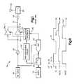
- FIG. 1is a schematic-block diagram illustration representing a prior art circuit
- FIG. 2is a graphical illustration of various waveforms illustrating a carrier wave and phase shifted carrier waves resulting from amplitude modulation which will be described herein to facilitate an understanding of the invention herein;
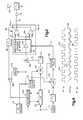
- FIG. 3is a schematic-block diagram illustration of one embodiment of the invention herein;
- FIG. 4is a graphical illustration showing waveforms illustrating the operation of a glitch filter employed in the embodiment of FIG. 3;
- FIG. 5is a schematic-block diagram illustration of a second embodiment of the invention herein.
- FIG. 6is a schematic-block diagram illustration of a phase modulator which may be employed in the embodiments of FIGS. 3 and 5 .
- FIG. 1This is a digital amplitude modulator similar to that illustrated and described in the aforesaid U.S. Swanson patents.
- the amplitude modulator 10is illustrated as receiving an input signal from an input signal source 12 , taking the form of an audio signal source. Another input to the modulator is an RF carrier signal obtained from an RF input source 14 .
- the modulatoramplitude modulates the RF carrier signal with the amplitude varying audio signal to provide at its output a modulated RF carrier signal which is then applied to an output network including an inductor 16 and a capacitor 18 and, thence, through a filter 20 to a load 22 , taking the form of an antenna.
- the amplitude varying audio signalis applied through a low pass filter 24 and is then converted into digital signals by an analog-to-digital converter 26 which is clocked at the frequency F c of the carrier signal.
- the digital words obtained from the analog-to-digital converter 26represent the amplitude values of samples of the audio signal and these are supplied to a modulation encoder 28 which then raises one or more of its output lines D 1 -DN to turn on one or more of a group of power amplifiers PA- 1 through PA-N in accordance with the value of the audio signal.
- the RF carrier signal supplied by the input source 14is applied through a buffer 30 and thence to each of the power amplifiers PA- 1 through PA-N, it being understood that only the power amplifiers PA- 1 through PA-N that arc turned on will amplify the carrier signal.
- the output signals of the power amplifiersare combined to provide a modulated RF carrier signal which is then supplied to the antenna 22 .
- This output modulated carrier signalexhibits the same frequency as the carrier signal supplied by the source 14 .
- the modulated RF carrier signalis phase shifted from the phase of the carrier signal applied to the power amplifiers by an amount that varies with the value of the amplitude varying signal supplied to the modulation encoder. This phase shift can be best understood with references to FIG. 2 .
- FIG. 2FIG.
- V iillustrates a squarewave carrier wave signal V i which is applied to the power amplifiers.
- This signalis made up of a plurality of squarewave pulses of constant magnitude and width and of a constant carrier frequency of F c .
- Waveform V o1represents an output amplitude modulated carrier frequency signal that has been shifted in phase so that it lags the applied carrier signal V i by a time delay T 1 .
- the amplitude of signal V o1is smaller than carrier signal V o2 .
- Carrier signal V o2lags carrier signal V i by a time delay T 2 .
- the phase shiftis not constant but varies with the amplitude of the amplitude varying audio signal. Consequently, this variable phase shift represents distortion which is of particular concern when the transmitter is intended to pass a phase modulated signal such as stereo CQAM or digital-in-band on channel (IBOC) digital radio signals.
- phase modulated signalsuch as stereo CQAM or digital-in-band on channel (I
- an adaptive approachto compensate for this variable phase shifting introduced by amplitude modulation.
- This adaptive approachprovides a constant phase shift regardless of the envelope or modulation level and is continuously adaptive to provide the best phase error correction.
- a modulator-amplifier network MAreceives RF carrier signals by way of a phase modulator PM, to be described in greater detail hereinafter, from a source of RF signals 14 .
- the modulator-amplifier network MAalso receives an audio signal A from an audio source 12 by way of filter 24 , an analog-to-digital converter 26 and an exciter field programmable gate array (FPGA) 40 .
- FPGAexciter field programmable gate array
- the FPGA 40provides a digital audio signal A to a modulation encoder and buffer 42 wherein the encoder portion provides a high or turn on signal on one or more of its output lines D 1 -DN to turn on one or more of the power amplifiers PA- 1 through PA-N with the number being turned on being dependent on the value of the amplitude varying audio signal.
- the carrier signal V iis supplied through a buffer 44 to each of the power amplifiers PA- 1 through P-N, it being understood that only the amplifiers that are turned on are effective to amplify the carrier signal.
- the audio signalis obtained from an audio source 12 and is applied to a low pass filter 24 prior to being digitized by a high speed analog-to-digital converter 26 which is clocked at the rate of the carrier frequency F c .
- a digital-to-analog converter 50to be described hereinafter, is also clocked at a rate corresponding with the carrier frequency. Both of these converters receive their clocking signals from a glitch filter 52 that is connected to the RF source 14 .
- the glitch filterreceives the input RF signal and removes any instantaneous phase reversal.
- FIG. 4illustrates an RF input signal having a glitch at 54 in waveform 56 .
- the filterincludes an integrator circuit and a high speed comparator to reconstruct the RF output signal 58 .
- the ramp signalis shown by the waveform 55 and the reference level for the high speed comparator by the dotted waveform 52 .
- the output of the analog-to-digital converter 26is applied to an exciter FPGA (field programmable gate array) 40 which then supplies a digitized audio signal A to the modulation encoder portion of the modulation amplifier network MA.
- the exciter FPGA 40applies a multi-bit (such as 14 bit) digital audio plus DC signal to an accumulator 60 and to a look up table (LUT) 62 .
- LUTlook up table
- a fixed delayis added to the audio plus DC signal to compensate for the audio pipeline delay stages in the exciter and modulation encoder processing. This signal is used to address the look up table 62 which provides + or ⁇ N° of phase delay which is then used to drive a high speed digital-to-analog converter 50 to create an analog voltage proportional to the desired carrier phase shift.
- This pre-shifted carrier signalis then supplied through buffer 44 to the power amplifiers PA- 1 through PA-N.
- a sample of the output voltage of the power amplifiersis feedback through a bandpass filter 66 to a phase detector 68 which also receives the output of the RF source 14 .
- the detector 68compares the transmitted carrier signal with the input carrier signal.
- the phase error detectorprovides an output as a binary 1 signal or a binary 0 signal with 1 being representative of a phase lead and the other being representative of a phase lag. This information is then supplied to the accumulator 60 .
- a phase lag signalindicates that the correction value at the address location in the look up table should be incremented whereas a phase lead signal indicates that the correction value should be decremented.
- the look up tablewill eventually reach a state wherein the values are changing by a least significant bit or the RMS error of the phase detector, whichever is greater. In this manner, the phase error is incrementally adjusted to nullify the error down to one bit of resolution.
- an alternative modulator-amplifier network MA 1which includes a single high power amplifier 71 whose gain is varied by an audio modulator 72 such that the gain of the amplifier varies with the magnitude of the audio signal.
- the amplitude modulated output carrier signalis supplied to the antenna 22 .
- a sample of the amplitude modulated carrier signalis applied through the band pass filter 66 to the phase detector 68 in the same manner as in the embodiment of FIG. 3 .
- phase modulatorphase shifter
- phase shifterphase shifter
- Any suitable phase shiftermay be employed that will perform this function.
- the phase shifter PM illustrated in FIG. 6is briefly described below and a more detailed description is presented in my aforesaid patent application Ser. No. 09/431,811 filed Nov. 2, 1999.
- This modulatorincludes a linear integrator 102 , a dual slope comparator 104 , a pair of pulse generators 106 and 108 and an S-R flip-flop 110 .
- the phase shiftis obtained proportional to the input phase shift control signal V c .
- Integrator 120is a linear integrator that converts each pulse cycle of the RF signal into a dual slope symmetrical ramp signal. This ramp signal Vramp varies in magnitude from a minimum level to a maximum level and then back to the minimum level for each pulse cycle.
- the control level signal V cis applied through an amplifier 112 to the negative or inverting input of an operational amplifier 114 .
- the output from the integrator 102is applied across a divider circuit including a resistor 116 and a capacitor 118 to ground.
- a reference voltage levelis taken at the junction of the resistor 116 and capacitor 118 and this voltage is applied to the positive or non-inverting input of the operational amplifier 114 .
- the output taken from amplifier 112 , voltage V ais supplied to the negative or inverting input of an operational amplifier serving as a voltage comparator 120 in the dual slope comparator 104 .
- the output voltage V b of operational amplifier 114is supplied to the positive input of an operational amplifier taking the form of a voltage comparator 122 in the dual slope comparator 104 .
- the ramp voltage obtained from the integrator 102is supplied to the positive input of comparator 120 and to the negative input of comparator 122 .
- the voltage V a obtained from amplifier 112 and the voltage V b obtained from amplifier 114are equally spaced in opposite directions from the reference voltage V 0 .
- the dual slope comparator 104compares the ramp voltage obtained from integrator 102 with the first and second level signals V a and V b and provides a first pulse signal and a second pulse signal.
- the first pulse signalhas a time duration corresponding with the time duration that the ramp signal exceeds the first voltage V a .
- the second pulse signalis provided for a time duration corresponding with the time duration that the second level signal V b exceeds the ramp signal.
- the pulse generators 106 and 108are respectively triggered by the leading edges of the positive output pulses taken from comparators 120 and 122 respectively.
- a bistable circuit taking the illustrative form of an S-R flip-flop 110includes a pair of logic gates 130 and 132 connected as shown. The SET and RESET ports of flip-flop 110 respectively receive trigger pulses from the pulse generators 106 and 108 to change from one state to the other.
- the output signal Xcorresponds in duty cycle with the original RF input signal.
- the output signal Xis shifted by a phase delay that is linearly proportional to the phase shift control signal V c .
Landscapes
- Engineering & Computer Science (AREA)
- Power Engineering (AREA)
- Physics & Mathematics (AREA)
- Nonlinear Science (AREA)
- Amplifiers (AREA)
- Digital Transmission Methods That Use Modulated Carrier Waves (AREA)
- Amplitude Modulation (AREA)
- Cable Transmission Systems, Equalization Of Radio And Reduction Of Echo (AREA)
- Noise Elimination (AREA)
Abstract
Description
Claims (11)
Priority Applications (5)
| Application Number | Priority Date | Filing Date | Title |
|---|---|---|---|
| US09/545,319US6285255B1 (en) | 1999-11-02 | 2000-04-07 | Adaptive compensation for carrier signal phase distortion |
| DE60135600TDE60135600D1 (en) | 2000-04-07 | 2001-03-27 | Adaptive compensation of the phase distortion of a carrier signal |
| EP01400783AEP1150422B1 (en) | 2000-04-07 | 2001-03-27 | Adaptive compensation for carrier signal phase distortion |
| CA002342417ACA2342417A1 (en) | 2000-04-07 | 2001-03-28 | Adaptive compensation for carrier signal phase |
| JP2001109968AJP2001358784A (en) | 2000-04-07 | 2001-04-09 | Adaptive compensation circuit and compensation method for carrier signal phase distortion |
Applications Claiming Priority (2)
| Application Number | Priority Date | Filing Date | Title |
|---|---|---|---|
| US09/431,811US6225864B1 (en) | 1999-11-02 | 1999-11-02 | RF amplifier having a dual slope phase modulator |
| US09/545,319US6285255B1 (en) | 1999-11-02 | 2000-04-07 | Adaptive compensation for carrier signal phase distortion |
Related Parent Applications (1)
| Application Number | Title | Priority Date | Filing Date |
|---|---|---|---|
| US09/431,811Continuation-In-PartUS6225864B1 (en) | 1999-11-02 | 1999-11-02 | RF amplifier having a dual slope phase modulator |
Publications (1)
| Publication Number | Publication Date |
|---|---|
| US6285255B1true US6285255B1 (en) | 2001-09-04 |
Family
ID=24175748
Family Applications (1)
| Application Number | Title | Priority Date | Filing Date |
|---|---|---|---|
| US09/545,319Expired - Fee RelatedUS6285255B1 (en) | 1999-11-02 | 2000-04-07 | Adaptive compensation for carrier signal phase distortion |
Country Status (5)
| Country | Link |
|---|---|
| US (1) | US6285255B1 (en) |
| EP (1) | EP1150422B1 (en) |
| JP (1) | JP2001358784A (en) |
| CA (1) | CA2342417A1 (en) |
| DE (1) | DE60135600D1 (en) |
Cited By (18)
| Publication number | Priority date | Publication date | Assignee | Title |
|---|---|---|---|---|
| US6429741B2 (en)* | 2000-06-13 | 2002-08-06 | Stmicroelectronics, S.R.L. | Circuit for detecting distortion in an amplifier, in particular an audio amplifier |
| US6459336B1 (en)* | 2000-10-11 | 2002-10-01 | Harris Corporation | RF amplifier system having PDM drive |
| US20020141510A1 (en)* | 2001-03-28 | 2002-10-03 | Ashvattha Semiconductor, Inc. | Method of and apparatus for performing modulation |
| US6640092B1 (en)* | 1998-02-20 | 2003-10-28 | Bae Systems Australia (Mbk) Pty Limited | Transmitter |
| KR20030085269A (en)* | 2002-04-30 | 2003-11-05 | 전자부품연구원 | Apparatus and method for controlling phase |
| US6720829B2 (en)* | 2001-12-25 | 2004-04-13 | Matsushita Electric Industrial Co., Ltd. | Distortion-compensated amplifying circuit |
| US6751265B1 (en)* | 2000-09-13 | 2004-06-15 | Tropian, Inc. | Method and system of amplitude modulation using dual/split channel unequal amplification |
| US20040136470A1 (en)* | 2003-01-15 | 2004-07-15 | Andrew Corporation | Uncorrelated adaptive predistorter |
| US20040259509A1 (en)* | 2003-06-19 | 2004-12-23 | Harris Corporation | Digitally adaptive modulated transmitter |
| US20050017801A1 (en)* | 2003-07-23 | 2005-01-27 | Andrew Corporation | Elimination of peak clipping and improved efficiency for RF power amplifiers with a predistorter |
| US20050024138A1 (en)* | 2003-07-31 | 2005-02-03 | Andrew Corporation | Predistorter for phase modulated signals with low peak to average ratios |
| US20050073360A1 (en)* | 2003-10-06 | 2005-04-07 | Andrew Corporation | Architecture and implementation methods of digital predistortion circuitry |
| US6972622B2 (en) | 2003-05-12 | 2005-12-06 | Andrew Corporation | Optimization of error loops in distributed power amplifiers |
| US7729668B2 (en) | 2003-04-03 | 2010-06-01 | Andrew Llc | Independence between paths that predistort for memory and memory-less distortion in power amplifiers |
| US8044716B1 (en)* | 2003-05-14 | 2011-10-25 | Marvell International Ltd. | Adjustable segmented power amplifier |
| US8195118B2 (en) | 2008-07-15 | 2012-06-05 | Linear Signal, Inc. | Apparatus, system, and method for integrated phase shifting and amplitude control of phased array signals |
| US8872719B2 (en) | 2009-11-09 | 2014-10-28 | Linear Signal, Inc. | Apparatus, system, and method for integrated modular phased array tile configuration |
| US20170180169A1 (en)* | 2015-12-18 | 2017-06-22 | Nxp Usa, Inc. | Method and apparatus for generating phase shift control signals |
Families Citing this family (3)
| Publication number | Priority date | Publication date | Assignee | Title |
|---|---|---|---|---|
| DE10131849A1 (en)* | 2001-06-27 | 2003-01-16 | Deutsche Telekom Ag | Procedure for avoiding interference emissions from AM transmitters for digital transmission |
| KR100991123B1 (en) | 2003-05-09 | 2010-11-02 | 톰슨 라이센싱 | Linear timecode receiver |
| US8625708B2 (en)* | 2010-09-08 | 2014-01-07 | Infineon Technologies Ag | Polar transmitter suitable for monolithic integration in SoCs |
Citations (7)
| Publication number | Priority date | Publication date | Assignee | Title |
|---|---|---|---|---|
| US4600892A (en)* | 1984-06-28 | 1986-07-15 | Hughes Aircraft Company | RF amplifier with frequency spectrum control |
| US4952890A (en) | 1989-09-12 | 1990-08-28 | Harris Corporation | Phase modulation compensated amplitude modulator using digitally selected amplifiers |
| US5049832A (en)* | 1990-04-20 | 1991-09-17 | Simon Fraser University | Amplifier linearization by adaptive predistortion |
| US5121077A (en)* | 1990-02-08 | 1992-06-09 | The Marconi Company Limted | Circuit for reducing distortion produced by an r.f. power amplifier |
| US5132637A (en) | 1991-03-25 | 1992-07-21 | Harris Corporation | RF power amplifier system having improved distortion reduction |
| US5247542A (en)* | 1990-04-23 | 1993-09-21 | Oki Electric Industry Co., Ltd. | QPSK power amplifier distortion correction system |
| US5798674A (en)* | 1997-04-08 | 1998-08-25 | Raytheon Company | Band Limited AM modulator using linear power amplification |
Family Cites Families (8)
| Publication number | Priority date | Publication date | Assignee | Title |
|---|---|---|---|---|
| JP2893719B2 (en)* | 1989-05-31 | 1999-05-24 | 日本電気株式会社 | Phase compensation circuit |
| JPH03198512A (en)* | 1989-12-27 | 1991-08-29 | Mitsubishi Electric Corp | high frequency amplifier |
| GB9002788D0 (en)* | 1990-02-08 | 1990-04-04 | Marconi Co Ltd | Circuit for reducing distortion produced by an r.f.power amplifier |
| US5101173A (en)* | 1990-11-28 | 1992-03-31 | The United States Of America As Represented By The Secretary Of The Air Force | Stored program controlled module amplifier bias and amplitude/phase compensation apparatus |
| US5101211A (en)* | 1991-01-10 | 1992-03-31 | Hughes Aircraft Company | Closed loop RF power amplifier output correction circuit |
| JPH04275708A (en)* | 1991-03-01 | 1992-10-01 | Nippon Telegr & Teleph Corp <Ntt> | Nonlinear distortion compensation circuit |
| JPH07263962A (en)* | 1994-03-17 | 1995-10-13 | Nec Corp | Linear compensation type amplitude modulating transmitter |
| SE506842C2 (en)* | 1996-06-28 | 1998-02-16 | Ericsson Telefon Ab L M | Device and method of radio transmitters for control of power amplifiers |
- 2000
- 2000-04-07USUS09/545,319patent/US6285255B1/ennot_activeExpired - Fee Related
- 2001
- 2001-03-27DEDE60135600Tpatent/DE60135600D1/ennot_activeExpired - Fee Related
- 2001-03-27EPEP01400783Apatent/EP1150422B1/ennot_activeExpired - Lifetime
- 2001-03-28CACA002342417Apatent/CA2342417A1/ennot_activeAbandoned
- 2001-04-09JPJP2001109968Apatent/JP2001358784A/enactivePending
Patent Citations (7)
| Publication number | Priority date | Publication date | Assignee | Title |
|---|---|---|---|---|
| US4600892A (en)* | 1984-06-28 | 1986-07-15 | Hughes Aircraft Company | RF amplifier with frequency spectrum control |
| US4952890A (en) | 1989-09-12 | 1990-08-28 | Harris Corporation | Phase modulation compensated amplitude modulator using digitally selected amplifiers |
| US5121077A (en)* | 1990-02-08 | 1992-06-09 | The Marconi Company Limted | Circuit for reducing distortion produced by an r.f. power amplifier |
| US5049832A (en)* | 1990-04-20 | 1991-09-17 | Simon Fraser University | Amplifier linearization by adaptive predistortion |
| US5247542A (en)* | 1990-04-23 | 1993-09-21 | Oki Electric Industry Co., Ltd. | QPSK power amplifier distortion correction system |
| US5132637A (en) | 1991-03-25 | 1992-07-21 | Harris Corporation | RF power amplifier system having improved distortion reduction |
| US5798674A (en)* | 1997-04-08 | 1998-08-25 | Raytheon Company | Band Limited AM modulator using linear power amplification |
Cited By (26)
| Publication number | Priority date | Publication date | Assignee | Title |
|---|---|---|---|---|
| US6640092B1 (en)* | 1998-02-20 | 2003-10-28 | Bae Systems Australia (Mbk) Pty Limited | Transmitter |
| US6429741B2 (en)* | 2000-06-13 | 2002-08-06 | Stmicroelectronics, S.R.L. | Circuit for detecting distortion in an amplifier, in particular an audio amplifier |
| US6751265B1 (en)* | 2000-09-13 | 2004-06-15 | Tropian, Inc. | Method and system of amplitude modulation using dual/split channel unequal amplification |
| US6459336B1 (en)* | 2000-10-11 | 2002-10-01 | Harris Corporation | RF amplifier system having PDM drive |
| US20020141510A1 (en)* | 2001-03-28 | 2002-10-03 | Ashvattha Semiconductor, Inc. | Method of and apparatus for performing modulation |
| US6937668B2 (en)* | 2001-03-28 | 2005-08-30 | Spectra Wireless, Inc. | Method of and apparatus for performing modulation |
| US6720829B2 (en)* | 2001-12-25 | 2004-04-13 | Matsushita Electric Industrial Co., Ltd. | Distortion-compensated amplifying circuit |
| KR20030085269A (en)* | 2002-04-30 | 2003-11-05 | 전자부품연구원 | Apparatus and method for controlling phase |
| US20040136470A1 (en)* | 2003-01-15 | 2004-07-15 | Andrew Corporation | Uncorrelated adaptive predistorter |
| US7403573B2 (en) | 2003-01-15 | 2008-07-22 | Andrew Corporation | Uncorrelated adaptive predistorter |
| US7729668B2 (en) | 2003-04-03 | 2010-06-01 | Andrew Llc | Independence between paths that predistort for memory and memory-less distortion in power amplifiers |
| US6972622B2 (en) | 2003-05-12 | 2005-12-06 | Andrew Corporation | Optimization of error loops in distributed power amplifiers |
| US8044716B1 (en)* | 2003-05-14 | 2011-10-25 | Marvell International Ltd. | Adjustable segmented power amplifier |
| EP1634379A4 (en)* | 2003-06-19 | 2007-06-27 | Harris Corp | Digitally adaptive modulated transmitter |
| US7035600B2 (en) | 2003-06-19 | 2006-04-25 | Harris Corporation | Digitally adaptive modulated transmitter |
| WO2005002071A1 (en)* | 2003-06-19 | 2005-01-06 | Harris Corporation | Digitally adaptive modulated transmitter |
| US20040259509A1 (en)* | 2003-06-19 | 2004-12-23 | Harris Corporation | Digitally adaptive modulated transmitter |
| US20050017801A1 (en)* | 2003-07-23 | 2005-01-27 | Andrew Corporation | Elimination of peak clipping and improved efficiency for RF power amplifiers with a predistorter |
| US6963242B2 (en) | 2003-07-31 | 2005-11-08 | Andrew Corporation | Predistorter for phase modulated signals with low peak to average ratios |
| US20050024138A1 (en)* | 2003-07-31 | 2005-02-03 | Andrew Corporation | Predistorter for phase modulated signals with low peak to average ratios |
| US20050073360A1 (en)* | 2003-10-06 | 2005-04-07 | Andrew Corporation | Architecture and implementation methods of digital predistortion circuitry |
| US7023273B2 (en) | 2003-10-06 | 2006-04-04 | Andrew Corporation | Architecture and implementation methods of digital predistortion circuitry |
| US8195118B2 (en) | 2008-07-15 | 2012-06-05 | Linear Signal, Inc. | Apparatus, system, and method for integrated phase shifting and amplitude control of phased array signals |
| US8872719B2 (en) | 2009-11-09 | 2014-10-28 | Linear Signal, Inc. | Apparatus, system, and method for integrated modular phased array tile configuration |
| US20170180169A1 (en)* | 2015-12-18 | 2017-06-22 | Nxp Usa, Inc. | Method and apparatus for generating phase shift control signals |
| US9973360B2 (en)* | 2015-12-18 | 2018-05-15 | Nxp Usa, Inc. | Method and apparatus for generating phase shift control signals |
Also Published As
| Publication number | Publication date |
|---|---|
| DE60135600D1 (en) | 2008-10-16 |
| EP1150422A2 (en) | 2001-10-31 |
| JP2001358784A (en) | 2001-12-26 |
| EP1150422A3 (en) | 2004-01-28 |
| EP1150422B1 (en) | 2008-09-03 |
| CA2342417A1 (en) | 2001-10-07 |
Similar Documents
| Publication | Publication Date | Title |
|---|---|---|
| US6285255B1 (en) | Adaptive compensation for carrier signal phase distortion | |
| US5249201A (en) | Transmission of multiple carrier signals in a nonlinear system | |
| US5021753A (en) | Splatter controlled amplifier | |
| US6130910A (en) | Method and apparatus for high efficiency wideband power amplification | |
| US6794931B2 (en) | Switched amplifier | |
| US6590940B1 (en) | Power modulation systems and methods that separately amplify low and high frequency portions of an amplitude waveform | |
| US7696818B2 (en) | Amplifying apparatus | |
| JP3644965B2 (en) | Efficient linear power amplification | |
| US6043707A (en) | Method and apparatus for operating a radio-frequency power amplifier as a variable-class linear amplifier | |
| US7068096B2 (en) | EER modulator with power amplifier having feedback loop providing soft output impedance | |
| US5469127A (en) | Amplification apparatus and method including modulator component | |
| CN1132389C (en) | Power 1-Q modulation systems and methods | |
| US4580111A (en) | Amplitude modulation using digitally selected carrier amplifiers | |
| US6252455B1 (en) | Method and apparatus for efficient signal amplification | |
| US20070018718A1 (en) | Microwave transmitter and the method for increasing envelope bandwidth | |
| Bolotov et al. | EER power amplifier modulator efficiency improvement using PWM with additional sigma-delta modulation | |
| US20050088226A1 (en) | Switching amplifier architecture | |
| CA2604480C (en) | A digital amplitude modulation transmitter with pulse width modulating rf drive | |
| JP2002500846A (en) | Low distortion power amplifier | |
| US6903619B2 (en) | Electromagnetic wave transmitter systems, methods and articles of manufacture | |
| US6771121B2 (en) | Linearization of a PDM Class-D amplifier | |
| JPH04156704A (en) | Linear power amplifier circuit | |
| US6225864B1 (en) | RF amplifier having a dual slope phase modulator | |
| US6100756A (en) | Method and apparatus for high efficiency power amplification | |
| Asbeck et al. | A polar linearisation system for RF power amplifiers |
Legal Events
| Date | Code | Title | Description |
|---|---|---|---|
| AS | Assignment | Owner name:HARRIS CORPORATION, FLORIDA Free format text:ASSIGNMENT OF ASSIGNORS INTEREST;ASSIGNORS:LUU, KY THOAI;DUELLO, WAYNE DOUGLAS;POSEY, DOUGLAS J.;REEL/FRAME:010983/0024;SIGNING DATES FROM 20000725 TO 20000727 | |
| FPAY | Fee payment | Year of fee payment:4 | |
| FPAY | Fee payment | Year of fee payment:8 | |
| AS | Assignment | Owner name:HBC SOLUTIONS, INC., COLORADO Free format text:ASSIGNMENT OF ASSIGNORS INTEREST;ASSIGNORS:HARRIS CORPORATION;EAGLE TECHNOLOGY INC.;REEL/FRAME:029759/0416 Effective date:20130204 | |
| AS | Assignment | Owner name:WILMINGTON TRUST, NATIONAL ASSOCIATION, MINNESOTA Free format text:SECURITY AGREEMENT;ASSIGNOR:HB CANADA COMMUNICATIONS LTD;REEL/FRAME:030156/0751 Effective date:20130329 Owner name:WILMINGTON TRUST, NATIONAL ASSOCIATION, MINNESOTA Free format text:SECURITY AGREEMENT;ASSIGNOR:HBC SOLUTIONS, INC.;REEL/FRAME:030156/0636 Effective date:20130204 | |
| AS | Assignment | Owner name:PNC BANK, NATIONAL ASSOCIATION, AS AGENT, NEW JERS Free format text:SECURITY AGREEMENT;ASSIGNOR:HBC SOLUTIONS, INC.;REEL/FRAME:030192/0355 Effective date:20130204 | |
| REMI | Maintenance fee reminder mailed | ||
| AS | Assignment | Owner name:HBC SOLUTIONS, INC., COLORADO Free format text:ASSIGNMENT OF ASSIGNORS INTEREST;ASSIGNORS:HARRIS CORPORATION;EAGLE TECHNOLOGY, LLC;REEL/FRAME:030333/0671 Effective date:20130204 | |
| LAPS | Lapse for failure to pay maintenance fees | ||
| STCH | Information on status: patent discontinuation | Free format text:PATENT EXPIRED DUE TO NONPAYMENT OF MAINTENANCE FEES UNDER 37 CFR 1.362 | |
| FP | Lapsed due to failure to pay maintenance fee | Effective date:20130904 |