US6285018B1 - Electron bombarded active pixel sensor - Google Patents
Electron bombarded active pixel sensorDownload PDFInfo
- Publication number
- US6285018B1 US6285018B1US09/356,800US35680099AUS6285018B1US 6285018 B1US6285018 B1US 6285018B1US 35680099 AUS35680099 AUS 35680099AUS 6285018 B1US6285018 B1US 6285018B1
- Authority
- US
- United States
- Prior art keywords
- active pixel
- pixel sensor
- photocathode
- vacuum
- electron
- Prior art date
- Legal status (The legal status is an assumption and is not a legal conclusion. Google has not performed a legal analysis and makes no representation as to the accuracy of the status listed.)
- Expired - Lifetime
Links
- 239000004065semiconductorSubstances0.000claimsdescription25
- 238000006243chemical reactionMethods0.000claimsdescription20
- 238000000034methodMethods0.000claimsdescription19
- 238000003384imaging methodMethods0.000claimsdescription17
- 238000012546transferMethods0.000claimsdescription17
- 239000000758substrateSubstances0.000claimsdescription14
- OAICVXFJPJFONN-UHFFFAOYSA-NPhosphorusChemical compound[P]OAICVXFJPJFONN-UHFFFAOYSA-N0.000claimsdescription7
- 230000004044responseEffects0.000claimsdescription3
- 238000009825accumulationMethods0.000claimsdescription2
- 239000003513alkaliSubstances0.000claimsdescription2
- 230000005684electric fieldEffects0.000claims3
- 238000007789sealingMethods0.000claims2
- 230000001681protective effectEffects0.000claims1
- 239000010410layerSubstances0.000description33
- 230000035945sensitivityEffects0.000description12
- 230000008569processEffects0.000description10
- 230000001133accelerationEffects0.000description9
- 238000012545processingMethods0.000description8
- 229910052710siliconInorganic materials0.000description8
- 239000010703siliconSubstances0.000description8
- XUIMIQQOPSSXEZ-UHFFFAOYSA-NSiliconChemical compound[Si]XUIMIQQOPSSXEZ-UHFFFAOYSA-N0.000description7
- 238000013459approachMethods0.000description7
- QTBSBXVTEAMEQO-UHFFFAOYSA-NAcetic acidChemical compoundCC(O)=OQTBSBXVTEAMEQO-UHFFFAOYSA-N0.000description6
- 101000694017Homo sapiens Sodium channel protein type 5 subunit alphaProteins0.000description6
- 230000008901benefitEffects0.000description6
- 238000009792diffusion processMethods0.000description6
- 230000004297night visionEffects0.000description6
- 230000003287optical effectEffects0.000description6
- 230000015556catabolic processEffects0.000description5
- 238000006731degradation reactionMethods0.000description5
- 239000000835fiberSubstances0.000description5
- 239000000463materialSubstances0.000description5
- 238000002161passivationMethods0.000description5
- KRHYYFGTRYWZRS-UHFFFAOYSA-NFluoraneChemical compoundFKRHYYFGTRYWZRS-UHFFFAOYSA-N0.000description4
- 230000010354integrationEffects0.000description4
- 230000005855radiationEffects0.000description4
- 230000009467reductionEffects0.000description4
- JBRZTFJDHDCESZ-UHFFFAOYSA-NAsGaChemical compound[As]#[Ga]JBRZTFJDHDCESZ-UHFFFAOYSA-N0.000description3
- 229910001218Gallium arsenideInorganic materials0.000description3
- 238000001444catalytic combustion detectionMethods0.000description3
- 238000001514detection methodMethods0.000description3
- 230000000694effectsEffects0.000description3
- 238000005516engineering processMethods0.000description3
- 238000004519manufacturing processMethods0.000description3
- 229910021420polycrystalline siliconInorganic materials0.000description3
- 229920005591polysiliconPolymers0.000description3
- 230000006798recombinationEffects0.000description3
- 238000005215recombinationMethods0.000description3
- 239000007787solidSubstances0.000description3
- MHAJPDPJQMAIIY-UHFFFAOYSA-NHydrogen peroxideChemical compoundOOMHAJPDPJQMAIIY-UHFFFAOYSA-N0.000description2
- GRYLNZFGIOXLOG-UHFFFAOYSA-NNitric acidChemical compoundO[N+]([O-])=OGRYLNZFGIOXLOG-UHFFFAOYSA-N0.000description2
- 229910052782aluminiumInorganic materials0.000description2
- XAGFODPZIPBFFR-UHFFFAOYSA-NaluminiumChemical compound[Al]XAGFODPZIPBFFR-UHFFFAOYSA-N0.000description2
- 239000000969carrierSubstances0.000description2
- 238000009826distributionMethods0.000description2
- 238000005530etchingMethods0.000description2
- 230000004907fluxEffects0.000description2
- 238000005286illuminationMethods0.000description2
- 230000007246mechanismEffects0.000description2
- 229910017604nitric acidInorganic materials0.000description2
- 238000001579optical reflectometryMethods0.000description2
- 238000005036potential barrierMethods0.000description2
- 229910000530Gallium indium arsenideInorganic materials0.000description1
- 238000010521absorption reactionMethods0.000description1
- 239000002253acidSubstances0.000description1
- 230000003321amplificationEffects0.000description1
- 238000000149argon plasma sinteringMethods0.000description1
- 239000002585baseSubstances0.000description1
- 230000005540biological transmissionEffects0.000description1
- 230000001010compromised effectEffects0.000description1
- 230000002596correlated effectEffects0.000description1
- 230000000875corresponding effectEffects0.000description1
- 238000010894electron beam technologyMethods0.000description1
- 238000005421electrostatic potentialMethods0.000description1
- 230000008030eliminationEffects0.000description1
- 238000003379elimination reactionMethods0.000description1
- 230000004927fusionEffects0.000description1
- 230000006872improvementEffects0.000description1
- 229910052751metalInorganic materials0.000description1
- 239000002184metalSubstances0.000description1
- 238000003199nucleic acid amplification methodMethods0.000description1
- 238000005457optimizationMethods0.000description1
- 239000011241protective layerSubstances0.000description1
- 238000005070samplingMethods0.000description1
- 230000003595spectral effectEffects0.000description1
- 238000010561standard procedureMethods0.000description1
- 238000003860storageMethods0.000description1
- 230000001131transforming effectEffects0.000description1
- 230000000007visual effectEffects0.000description1
Images


Classifications
- H—ELECTRICITY
- H01—ELECTRIC ELEMENTS
- H01J—ELECTRIC DISCHARGE TUBES OR DISCHARGE LAMPS
- H01J31/00—Cathode ray tubes; Electron beam tubes
- H01J31/08—Cathode ray tubes; Electron beam tubes having a screen on or from which an image or pattern is formed, picked up, converted, or stored
- H01J31/26—Image pick-up tubes having an input of visible light and electric output
- H—ELECTRICITY
- H04—ELECTRIC COMMUNICATION TECHNIQUE
- H04N—PICTORIAL COMMUNICATION, e.g. TELEVISION
- H04N23/00—Cameras or camera modules comprising electronic image sensors; Control thereof
- H04N23/20—Cameras or camera modules comprising electronic image sensors; Control thereof for generating image signals from infrared radiation only
- H—ELECTRICITY
- H04—ELECTRIC COMMUNICATION TECHNIQUE
- H04N—PICTORIAL COMMUNICATION, e.g. TELEVISION
- H04N25/00—Circuitry of solid-state image sensors [SSIS]; Control thereof
- H—ELECTRICITY
- H10—SEMICONDUCTOR DEVICES; ELECTRIC SOLID-STATE DEVICES NOT OTHERWISE PROVIDED FOR
- H10F—INORGANIC SEMICONDUCTOR DEVICES SENSITIVE TO INFRARED RADIATION, LIGHT, ELECTROMAGNETIC RADIATION OF SHORTER WAVELENGTH OR CORPUSCULAR RADIATION
- H10F39/00—Integrated devices, or assemblies of multiple devices, comprising at least one element covered by group H10F30/00, e.g. radiation detectors comprising photodiode arrays
- H10F39/10—Integrated devices
- H10F39/12—Image sensors
- H10F39/18—Complementary metal-oxide-semiconductor [CMOS] image sensors; Photodiode array image sensors
- H—ELECTRICITY
- H10—SEMICONDUCTOR DEVICES; ELECTRIC SOLID-STATE DEVICES NOT OTHERWISE PROVIDED FOR
- H10F—INORGANIC SEMICONDUCTOR DEVICES SENSITIVE TO INFRARED RADIATION, LIGHT, ELECTROMAGNETIC RADIATION OF SHORTER WAVELENGTH OR CORPUSCULAR RADIATION
- H10F39/00—Integrated devices, or assemblies of multiple devices, comprising at least one element covered by group H10F30/00, e.g. radiation detectors comprising photodiode arrays
- H10F39/10—Integrated devices
- H10F39/12—Image sensors
- H10F39/199—Back-illuminated image sensors
- H—ELECTRICITY
- H10—SEMICONDUCTOR DEVICES; ELECTRIC SOLID-STATE DEVICES NOT OTHERWISE PROVIDED FOR
- H10F—INORGANIC SEMICONDUCTOR DEVICES SENSITIVE TO INFRARED RADIATION, LIGHT, ELECTROMAGNETIC RADIATION OF SHORTER WAVELENGTH OR CORPUSCULAR RADIATION
- H10F39/00—Integrated devices, or assemblies of multiple devices, comprising at least one element covered by group H10F30/00, e.g. radiation detectors comprising photodiode arrays
- H10F39/80—Constructional details of image sensors
- H10F39/803—Pixels having integrated switching, control, storage or amplification elements
Definitions
- This inventionrelates to devices and methods to image or detect a useful image at low light levels utilizing an active pixel sensor in an electron bombarded mode using a photocathode for detection or imaging at low light levels.
- Cameras that operate at low light levelshave a number of significant applications in diverse areas. These include, among others, photographic, night vision, surveillance, and scientific uses. Modern night vision systems, for example, are rapidly transforming presently used direct view systems to camera based arrangements. These are driven by the continued advances in video display and processing. Video based systems allow remote display and viewing, recording, and image processing including fusion with other imagery such as from a forward looking infra-red sensor. Surveillance applications are also becoming predominately video based where camera size, performance, and low light level sensitivity are often critical. Scientific applications require cameras with good photon sensitivity over a large spectral range and high frame rates. These applications, and others, are driving the need for improved low light level sensors with direct video output.
- Image sensing deviceswhich incorporate an array of image sensing pixels are commonly used in electronic cameras. Each pixel produces an output signal in response to incident light. The signals are read out, typically one row at a time, to form an image. Cameras in the art have utilized Charge Coupled Devices (CCD) as the image sensor. Image sensors which incorporate an amplifier into each pixel for increased sensitivity are known as active pixel sensors (sometimes referred to herein as APS). Active pixel sensors are disclosed, for example in U.S. Pat. No. 5,789,774 issued Aug. 4, 1998 to Merrill; U.S. Pat. No. 5,631,704 issued May 20, 1997 to Dickinson et al; U.S. Pat. No.
- the cameraIn general, it is desirable to provide cameras which generate high quality images over a wide range of light levels including to extremely low light levels such as those encountered under starlight and lower illumination levels.
- the camerashould have a small physical size and low electrical power requirements, thereby making portable, head-mounted, and other battery-operated applications practical.
- Active pixel sensor camerasmeet the small size and low power requirements, but have poor low light level sensitivity with performance limited to conditions with 0.1 lux (twilight) or higher light levels.
- Night vision cameraswhich operate under extremely low light levels are known in the art.
- the standard low light level cameras in use todayare based on a Generation-III (GaAs photocathode) or Generation-II (multi-alkali photocathode) image intensifier fiber optically coupled to a CCD to form an Image Intensified CCD or ICCD camera.
- the scene to be imagedis focused by the input lens onto the photocathode faceplate assembly.
- the impinging light energyliberates photoelectrons from the photocathode to form an electron image.
- the electron imageis proximity focused onto the input of the microchannel plate (MCP) electron multiplier, which intensifies the electron image by secondary multiplication while maintaining the geometric integrity of the image.
- MCPmicrochannel plate
- the intensified electron imageis proximity focused onto a phosphor screen, which converts the electron image back to a visible image, which typically is viewed through a fiber optic output window.
- a fiber optic taper or transfer lensthen transfers this amplified visual image to a standard CCD sensor, which converts the light image into electrons which form a video signal.
- ICCD camerasthere are five interfaces at which the image is sampled, and each interface degrades the resolution and adds noise to the signal of the ICCD camera. This image degradation which has heretofore not been avoidable, is a significant disadvantage in systems requiring high quality output.
- the ICCD sensortends also to be large and heavy due to the fused fiber optic components.
- a surveillance system having a Generation-II MCP image intensifier tubeis described, for example, in U.S. Pat. No. 5,373,320 issued Dec. 13, 1994 to Johnson et al.
- a camera attachment described in this patentconverts a standard daylight video camera into a day/night video camera.
- Kfis defined as the ratio of the Signal-to-Noise power ratio at the input of the MCP divided by the Signal-to-Noise power ratio at the output of the MCP after amplification.
- Kfis a measure of the degradation of the image Signal-to-Noise ratio due to the MCP gain process.
- Typical values for Kfare 4.0 for a Generation-III image intensifier. A low noise, high gain.
- MCP for use in Generation-III image intensifiersis disclosed in U.S. Pat. No. 5,268,612 issued Dec. 7, 1993 to Aebi et al.
- EBSelectron-bombarded semiconductor
- gainis achieved by electron multiplication resulting when the high velocity electron beam dissipates its energy in a semiconductor.
- the dissipated energycreates electron-hole pairs.
- the semiconductor siliconone electron-hole pair is created for approximately every 3.6 electron-volt (eV) of incident energy.
- eVelectron-volt
- the electron-bombarded semiconductor gain processhas been utilized in a focused electron bombarded hybrid photomultiplier tube comprising a photocathode, focusing electrodes and a collection anode consisting of a semiconductor diode disposed in a detector body as disclosed in U.S. Pat. No. 5,374,826 issued Dec. 20, 1994 to LaRue et al. and U.S. Pat. No. 5,475,227 issued Dec. 12, 1995 to LaRue.
- the disclosed hybrid photomultiplier tubesare highly sensitive but do not sense images.
- the electron-bombarded semiconductor gain processhas been used to address image degradation in the ICCD low light level camera.
- a back illuminated CCDis used as an anode in proximity focus with the photocathode to form an Electron Bombarded CCD (EBCCD).
- EBCCDElectron Bombarded CCD
- Photoelectrons from the photocathodeare accelerated to and imaged in the back illuminated CCD directly.
- Gainis achieved by the low noise electron-bombarded semiconductor gain process.
- the EBCCDeliminates the MCP, phosphor screen, and fiber optics, and as a result both improved image quality and increased sensitivity can be obtained in a smaller sized camera.
- Significant improvement of the degraded resolution and high noise of the conventional image transfer chainhas been realized with the EBCCD.
- EBCCDis disclosed in U.S. Pat. No. 4,687,922 issued Aug. 18, 1987 to Lemonier. Extensive background on EBCCDs is contained in the paper by Aebi, et al, “Gallium Arsenide Electron Bombarded CCD Technology”, SPIE Vol. 3434, pp. 37-44, (1998) and references cited therein.
- Optimum low light level EBCCD performancerequires a specialized CCD.
- the CCDis required to be backside thinned to allow high electron-bombarded semiconductor gain.
- the CCDcannot be used in a frontside bombarded mode as used in a standard CCD camera as the gate structures would block the photoelectrons from reaching the semiconductor and low electron-bombarded semiconductor gains would be obtained at moderate acceleration voltages High acceleration voltages required to penetrate the gate structures would cause radiation damage to the CCD and shorten CCD operating life.
- a frame transfer formatis required where the CCD has both an imaging region and a store region on the chip. The image and store regions are of approximately the same size. A frame transfer format is required for two reasons.
- the CCD imaging areahave high fill factor (minimum dead area) if possible.
- the frame transfer CCD architecturesatisfies this requirement.
- the interline transfer CCD architecturewould result in substantial dead area (of order 70-80%). Any reduction in active area will result in lost photoelectrons. This is equivalent to a reduction in photocathode quantum efficiency or sensitivity.
- At the lowest light levels (starlight or overcast starlight)low light level camera performance is dictated by the photon statistics. It is essential that the maximum number of photons be detected by the imager for adequate low light level resolution and performance.
- Second a frame transfer formatallows signal integration to occur during the readout of the store region in addition to any integration period. This allows charge to be integrated almost continuously maximizing the collected signal.
- EBCCD camerashave several other disadvantages.
- the frame transfer CCD architecturehas the serious disadvantage for the EBCCD application of essentially doubling the size of the required vacuum envelope due to the requirement for image and store regions on the CCD. This requirement also means that the frame transfer CCD chip is over twice the size of the image area. This substantially increases the cost of the COD relative to interline transfer CCDs or active pixel sensor chips as fewer chips can be fabricated per silicon wafer.
- EBCCD based camerasalso have the disadvantage of backside illumination of the CCD which necessitates specialized processing to thin the semiconductor and passivate the back surface for high electron-bombarded semiconductor gain. This processing is not standard in the silicon industry and substantially increases the EBCCD manufacturing cost.
- the EBCCD camerasconsume several watts of power due to the CCD clocking requirements and require external electronics for a complete camera.
- the size of the external camera electronicspresents an obstacle to applications that would benefit from miniaturization of the camera.
- CCDsrequire specialized semiconductor processing lines which are not compatible with mainstream CMOS semiconductor fabrication technology. This further increases the cost of CCD based cameras.
- CMOS imagerin an electron bombarded mode in a vacuum envelope with a photocathode sensor.
- the electron bombarded active pixel sensorconstitutes a complete low light level camera with the addition of a lens, housing, power, and a control interface.
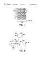
- FIG. 1is a schematic illustration of the architecture of an active pixel sensor chip
- FIG. 2is a schematic illustration of the architecture of a photogate type active pixel sensor
- FIG. 3is a schematic illustration of the architecture of a typical photodiode type of active pixel sensor
- FIG. 4is a schematic illustration showing an electron bombarded active pixel sensor in a vacuum tube arrangement in accordance with the present invention
- FIG. 5is a cross sectional view of a photodiode pixel structure
- FIG. 6is a schematic illustration of an active pixel sensor with an overlying light conversion layer
- FIG. 7is an showing of an imaging system or camera illustrating an application of this invention.
- FIG. 1An active pixel sensor chip is illustrated in FIG. 1 .
- the architecture of a photogate active pixel sensoris shown in FIG. 2 and of a photodiode active pixel sensor in FIG. 3 .
- FIG. 1there is shown a pixel array 11 controlled by a logic timing and control circuit 12 .
- Signalsare processed by signal processors 13 which may comprise an analog signal processor and analog to digital converters.
- a column select control circuitis illustrated as 15 and the output signal is shown feeding from the active pixel sensor by an arrow designated 16 .
- the output at 16may comprise a digital or analog signal depending on the system in which the active pixel sensor is being used or to which the signal is being fed.
- the first architecture for the pixelis the photogate pixel structure.
- the second pixel architectureis the photodiode pixel structure.
- FIG. 2there is illustrated a photogate type pixel structure.
- the photoelectrons generated by the incident photon fluxare integrated under photogate, 74 .
- the photogatewhich is similar to a gate formed on a CCD, comprises a polysilicon electrode on a dielectric layer over the charge storage region.
- the photogateis biased by the voltage source applied to 67 .
- the photogateis separated from the floating output diffusion node 72 , by the transfer gate 75 and the bridging diffusion 73 .
- the transfer gateis biased by the voltage source applied to 66 .
- the potential wells generated by these applied bias voltages in the semiconductorare illustrated by dotted line 71 with the photogate voltage bias applied to allow charge integration under the photogate.
- the floating output diffusion nodeis reset by the voltage source applied to 61 (also referred to as Drain Voltage) which is applied when gate 62 of the normally off reset transistor 64 is pulsed by a voltage source to turn the transistor on and set the floating output diffusion to the drain voltage.
- the photogate voltageis then pulsed momentarily to transfer any collected charge to the floating output diffusion node 72 .
- the photogenerated chargeis sensed when the row select transistor 63 is turned on by applying a voltage pulse to transistor gate 69 .
- the chargeis amplified by the source follower transistor 59 and the voltage is sensed by the analog signal processing circuit 13 (see FIG. 1) connected to the column bus 65 .
- the photogate structure(FIG. 2 ), as compared to the photodiode pixel structure illustrated in FIG.
- FIG. 3there is illustrated a photodiode type pixel structure.
- the photoelectrons generated by the incident photon fluxare collected on the photodiode 20 which has been reverse biased by the voltage source applied to 21 (also referred to as Drain Voltage) which is applied when gate 22 of the normally off reset transistor 24 is pulsed by a voltage source to turn the transistor on and set the photodiode bias to the drain voltage.
- the photogenerated chargeis sensed when the row select transistor 23 is turned on by applying a voltage pulse to transistor gate 29 .
- the chargeis amplified by the source follower transistor 19 and the voltage is sensed by the analog signal processing circuit 13 (see FIG. 1) connected to the column bus 25 .
- Active pixel sensor based camerashave significant advantages over charge coupled device based cameras. These advantages include: substantially higher levels of electronics integration with the majority of the required camera electronics integrated on the APS chip where the electronics include integrated timing and control electronics; an order of magnitude or greater reduction in power requirements; use of low cost standard CMOS fabrication technology; substantial overall reduction in camera volume; and versatile image readout.
- Image readout modescan include window readout of subregions of the overall array or skip readout where every n th pixel is readout (n being an integer). In both of these modes only a fraction of the pixels are readout enabling higher frame rates.
- FIG. 4there is shown an electron bombarded active pixel sensor vacuum system or tube 33 in accordance with this invention.
- This systemmay comprise photocathode 31 , preferably a III-V semiconductor photocathode such as GaAs or an InP/InGaAs Transferred Electron photocathode for high performance applications, in proximity focus with a specialized active pixel sensor chip 32 which forms the anode of tube 33 .
- Photoelectrons 35are emitted from photocathode 31 in response to incident light illustrated as arrows designated 36 . These electrons are accelerated by an applied voltage to sufficient energy to allow electron gain in the chip in which the active pixel sensor 32 is found.
- the acceleration voltage 37 applied to photocathode 31is negative with respect to the chip. This permits biasing of the chip to be near ground potential for easy interfacing with other components.
- Control signals and bias voltages 38are applied to active pixel sensor 32 and a video output signal 40 may be taken off sensor 32 .
- the base of tube 31in FIG. 4 is a transparent faceplate 41 and tube sidewalls 39 extend between the transparent faceplate 41 on which the photocathode 31 is positioned and header assembly 34 , on which the APS chip is positioned.
- the header assembly 34also provides means for electrical feedthroughs for applying voltages 38 to the APS chip and for video output signals 40 from the APS chip.
- Electron bombarded sensor gainis preferably high enough to overcome readout noise. This will allow detection of a single photoelectron.
- the active pixel sensor for this applicationis modified for electron sensitivity using the electron-bombarded semiconductor mechanism.
- the preferred embodimentis a frontside electron bombarded mode to eliminate the requirement for backside thinning and passivation of the active pixel sensor chip.
- the frontside electron bombarded approachwill result in the lowest cost electron bombarded active pixel sensor component.
- An electron bombarded active pixel sensor component incorporating a frontside electron bombarded active pixel sensor chippreferably uses a photodiode active pixel architecture. This is because all overlying materials can be removed to the photodiode semiconductor surface with this pixel arrangement. Intervening materials between the semiconductor and the incident electrons could absorb the electrons and dissipate the electron energy resulting in low electron-bombarded semiconductor gain or requiring high acceleration voltages.
- a photogate active pixel sensor architecturehas the disadvantage of requiring overlying polysilicon or other materials which would interfere with collection of the incident photoelectrons for typical acceleration energies (2 keV). The incident electrons may also cause radiation damage to the dielectric—Silicon interface resulting in short operation life for a frontside electron bombarded photogate active pixel sensor chip.
- the photodiodeis desired to have high electron-bombarded semiconductor gain at relatively low electron acceleration voltages (preferably less than 2,000 volts). This minimizes radiation damage to the CMOS imager due to x-rays generated by electron bombardment of the silicon or overlying structures on the active pixel sensor chip. Low voltage operation is also desirable to enable easy gating of the tube by control of the applied voltage. Furthermore it is desirable to shield adjacent CMOS circuitry from the electron bombardment by providing an overlying protective layer with conductivity to allow any charge accumulation to be drained, preventing damage due to electrostatic discharge. The shielding also reduces x-ray dose to the underlying CMOS circuitry.
- High electron-bombarded semiconductor gain at low electron acceleration voltagesrequires elimination of any overlayers from the photodiode surface and good passivation of the semiconductor surface to minimize carrier recombination at the surface.
- This passivationcan be achieved by a number of techniques known to the art.
- One standard techniqueis to form a thin doped region at the semiconductor surface. The thickness of this doped region is desired to be less than or equal to the electron range in the solid, preferably substantially less, at the desired operating voltage. For operation at 2,000 volts the electron range is approximately 600 ⁇ for silicon.
- the doped regionis doped to have a greater free carrier concentration of the same carrier type than the underlying region. This increase in doping concentration forms a potential barrier which prevents the desired minority carriers from reaching the surface where they could recombine and not be collected by the reverse biased photodiode.
- Other techniques to form a potential barrier to prevent minority carriers from reaching the surfaceare known in the art. Passivation techniques are disclosed, for example, in U.S. Pat. No. 4,822,748 issued Apr. 18, 1989 to Janesick et al; and in U.S. Pat. No. 4,760,031 issued Jul. 26, 1988 to Janesick.
- An alternate embodiment of this inventionutilizes a backside bombarded active pixel sensor chip.
- the APS chipis mounted face down and the silicon substrate is mechanically and chemically removed leaving a thinned active pixel sensor chip
- FIG. 5A cross section of a photodiode pixel structure is illustrated in FIG. 5 prior to thinning of the substrate.
- the photodiode, 20 in FIG. 3,is indicated as region 55 in FIG. 5 .
- the CMOS circuitry composed of the associated transistors in the pixel (transistors 19 , 22 , and 23 in FIG. 3)are contained in region 53 .
- First a rapid isotropic etching stepis performed to remove a major portion of substrate 51 . For example, if the substrate is approximately 400 ⁇ m initially, this etch step will proceed until approximately 380 ⁇ m of the substrate layer 51 has been etched away leaving a thin layer of approximately 20 ⁇ m of substrate material.
- This etch stepis performed with the aid of a solution of nitric acid, acetic acid and hydrofluoric acid in proportions of 5:3:3 or through the use of similar solutions known in the art.
- a final thickness of good consistencywill be produced.
- a slow etchis then carried out in order to remove the remaining substrate material, stopping the etch in layer 57 . This leaves a layer which is on the order of 5 ⁇ m thick.
- This etchis done with the aid of a solution of nitric acid, acetic acid and hydrofluoric acid in proportions of 3:8:1, in the presence of hydrogen peroxide in the ratio of 5 ml per 350 ml of acid solution or using similar solutions known in the art.
- etch selectivityDoping differences between layers 57 and 51 are utilized to obtain etch selectivity. Etching is performed to assure good uniformity in thickness. After thinning of the active pixel sensor the back surface is passivated to reduce the surface recombination velocity and ensure high electron bombarded gain at low operation voltages ( ⁇ 2 kV).
- Substrate removal and backside passivationenables the photons and photoelectrons to be absorbed at a point sufficiently close to the sources of potential and charge collection which in this embodiment is performed with a reverse biased photodiode to allow charges created to reach their destinations without bulk or surface recombination or lateral diffusion.
- a less preferred, alternate embodiment of this inventionutilizes a frontside bombarded active pixel sensor chip coated with an electron-to-light conversion layer. This is now discussed in connection with FIG. 6 hereof.
- FIG. 6An active pixel sensor of this type is shown in FIG. 6 .
- FIG. 6there is shown a cross section of an active pixel sensor with a front side electron-to-light conversion layer.
- the photodiode ( 20 in FIG. 3) or photogate ( 74 in FIG. 2)is indicated as region 85 in FIG. 6 .
- the CMOS circuitrycomposed of the associated transistors or gates in the pixel (transistors 19 , 22 , and 23 in FIG. 3 or transistors and gates 75 , 64 , 63 , 59 in FIG. 2) are contained in region 83 . These structures are contained in substrate 81 .
- An optical shield layer 86is used to block light generated in electron-to-light conversion layer 84 from entering region 83 .
- Layer 86may be fabricated from aluminum or other highly reflective metal to allow generated light to be reflected back into the light conversion layer where further reflections may result in the light reaching region 85 where it will be detected by the photodiode or photogate structure.
- the light conversion layer, 84is coated with an optically reflective, electrically conductive layer 82 .
- Layer 82forms a conductive anode layer for the electron bombarded active pixel sensor and allows the incident electrons to be collected and to drain off to the tube bias voltage supply. Layer 82 also blocks light generated in layer 84 from reaching the photocathode.
- layer 82must attenuate light reaching the photocathode from layer 84 by at least three orders of magnitude or more to minimize optical feedback effects.
- a standard active pixel sensor chipmay be used with application of the electron-to-light conversion layer and associated structure shown in FIG. 6 . Electrons accelerated from the cathode to anode are converted to photons by the conversion layer which are detected by the APS pixel. This screen would be deposited directly on the active pixel sensor chip.
- layer 82would be fabricated using aluminum which has the properties of good optical reflectivity and good electron transmission at relatively low incident electron energies. Optical reflectivity is important to allow more of the generated light to reach the photogate or photodiode for greater sensitivity. In this case light which strikes layer 82 may be reflected back to the pixel and be detected, increasing screen efficiency.
- Layer 84may be fabricated using high efficiency phosphors such as P20 or P43, which emit in the green. Further optimization may be done by choosing a phosphor that emits light with a wavelength which matches the peak sensitvity wavelength of the active pixel sensor.
- the conversion layermay comprise a standard metallized phosphor screen of the type known in the art.
- FIG. 7there is shown an illustration of a camera in accordance with this invention intended to be illustrative of any number of different imaging systems.
- 140represents an image which is focused through lens 141 onto photocathode 142 .
- voltage lead 143from voltage source 145 .
- Voltage source 145is also connected through lead 146 to active pixel sensor 147 .
- a vacuum chamber 148separates photocathode 142 from active pixel sensor 147 .
- Walls 150indicate the outer sealed walls of the chamber
- the camera arrangement shown in this figureis intended to illustrate a system useful in connection with this invention.
- the camera systemmay take many forms and may be modified as is known in the art for a particular application.
- the image being capturedmay comprise the inside or the outside of a building area with the camera lens focusing images onto the photocathode which in turn in space wise configuration transfers the image to the active pixel sensor which in turn may feed an output cathode ray system or alternate display for viewing of the image.
- the image 140may be viewed at a remote location or on a display integrated in the system to which the output of the active pixel sensor is fed. Such a screen may located as shown at 154 as the output of the system.
- a camera of the type illustratedis capable of imaging and reproducing images working at light levels as low as starlight but typically and preferably will be operated in brighter surroundings but such surroundings may be without adequate light for normal passage of persons at nighttime. This generally is more than adequate for most systems and needs and thus permits the setting of lower standards for certain components used in the system.
- the systemwould be designed as illustrated and may include some of the unique approaches followed for night vision devices such as battery operations, helmet arrangements and the like.
Landscapes
- Engineering & Computer Science (AREA)
- Multimedia (AREA)
- Signal Processing (AREA)
- Solid State Image Pick-Up Elements (AREA)
- Image-Pickup Tubes, Image-Amplification Tubes, And Storage Tubes (AREA)
- Studio Devices (AREA)
- Transforming Light Signals Into Electric Signals (AREA)
- Photometry And Measurement Of Optical Pulse Characteristics (AREA)
Abstract
Description
Claims (25)
Priority Applications (8)
| Application Number | Priority Date | Filing Date | Title |
|---|---|---|---|
| US09/356,800US6285018B1 (en) | 1999-07-20 | 1999-07-20 | Electron bombarded active pixel sensor |
| EP02025164AEP1306906B1 (en) | 1999-07-20 | 2000-07-14 | Electron bombarded active pixel sensor |
| JP2001519132AJP5430810B2 (en) | 1999-07-20 | 2000-07-14 | Electron impact active pixel sensor |
| PCT/US2000/019474WO2001006571A1 (en) | 1999-07-20 | 2000-07-14 | Electron bombarded active pixel sensor |
| AU61073/00AAU6107300A (en) | 1999-07-20 | 2000-07-14 | Electron bombarded active pixel sensor |
| CA002379956ACA2379956C (en) | 1999-07-20 | 2000-07-14 | Electron bombarded active pixel sensor |
| EP00947471AEP1204993A4 (en) | 1999-07-20 | 2000-07-14 | ELECTRON BOMBARDED ACTIVE PIXEL SENSOR |
| US09/784,621US6657178B2 (en) | 1999-07-20 | 2001-02-14 | Electron bombarded passive pixel sensor imaging |
Applications Claiming Priority (1)
| Application Number | Priority Date | Filing Date | Title |
|---|---|---|---|
| US09/356,800US6285018B1 (en) | 1999-07-20 | 1999-07-20 | Electron bombarded active pixel sensor |
Related Child Applications (1)
| Application Number | Title | Priority Date | Filing Date |
|---|---|---|---|
| US09/784,621Continuation-In-PartUS6657178B2 (en) | 1999-07-20 | 2001-02-14 | Electron bombarded passive pixel sensor imaging |
Publications (1)
| Publication Number | Publication Date |
|---|---|
| US6285018B1true US6285018B1 (en) | 2001-09-04 |
Family
ID=23403000
Family Applications (1)
| Application Number | Title | Priority Date | Filing Date |
|---|---|---|---|
| US09/356,800Expired - LifetimeUS6285018B1 (en) | 1999-07-20 | 1999-07-20 | Electron bombarded active pixel sensor |
Country Status (6)
| Country | Link |
|---|---|
| US (1) | US6285018B1 (en) |
| EP (2) | EP1204993A4 (en) |
| JP (1) | JP5430810B2 (en) |
| AU (1) | AU6107300A (en) |
| CA (1) | CA2379956C (en) |
| WO (1) | WO2001006571A1 (en) |
Cited By (63)
| Publication number | Priority date | Publication date | Assignee | Title |
|---|---|---|---|---|
| WO2003024091A1 (en)* | 2000-11-16 | 2003-03-20 | California Institute Of Technology | Photodiode cmos imager with column-feedback soft-reset |
| US20030137243A1 (en)* | 2000-08-31 | 2003-07-24 | Costello Kenneth A. | Unitary vacuum tube incorporating high voltage isolation |
| US6747258B2 (en) | 2001-10-09 | 2004-06-08 | Itt Manufacturing Enterprises, Inc. | Intensified hybrid solid-state sensor with an insulating layer |
| US20040149888A1 (en)* | 2003-01-31 | 2004-08-05 | Intevac, Inc. | Backthinned CMOS sensor with low fixed pattern noise |
| US20040180462A1 (en)* | 2003-01-31 | 2004-09-16 | Intevac, Inc. | Backside thinning of image array devices |
| US20040245593A1 (en)* | 2003-01-31 | 2004-12-09 | Costello Kenneth A. | Backside thinning of image array devices |
| EP1532686A2 (en)* | 2002-07-11 | 2005-05-25 | Qinetiq Limited | Photodetector circuits |
| US20050161703A1 (en)* | 2004-01-23 | 2005-07-28 | Intevac, Inc. | Wavelength extension for backthinned silicon image arrays |
| US20050167575A1 (en)* | 2001-10-09 | 2005-08-04 | Benz Rudolph G. | Intensified hybrid solid-state sensor |
| US20050253242A1 (en)* | 2004-05-14 | 2005-11-17 | Intevac, Inc. | Semiconductor die attachment for high vacuum tubes |
| US20050258212A1 (en)* | 2004-05-14 | 2005-11-24 | Intevac, Inc. | Semiconductor die attachment for high vacuum tubes |
| US7006741B1 (en)* | 2005-03-22 | 2006-02-28 | Bi Yu | Contact-field optical microscope |
| US20060077269A1 (en)* | 2002-03-15 | 2006-04-13 | National Semiconductor Corporation | Pixel binning image sensor |
| US20060169901A1 (en)* | 2004-12-08 | 2006-08-03 | The Regents Of The University Of California | Direct collection transmission electron microscopy |
| GB2426649A (en)* | 2005-05-25 | 2006-11-29 | Motorola Inc | Sleeve for mounting between a lens and sensor |
| US20090050946A1 (en)* | 2004-07-25 | 2009-02-26 | Jacques Duparre | Camera module, array based thereon, and method for the production thereof |
| US20090278929A1 (en)* | 2008-05-06 | 2009-11-12 | Flir Systems Inc | Video camera with interchangable optical sensors |
| US20100123082A1 (en)* | 2008-11-18 | 2010-05-20 | Gatan, Inc. | Method for electron back-illumination of a semiconductor image sensor |
| US20100230729A1 (en)* | 2009-03-10 | 2010-09-16 | International Business Machines Corporation | Pixel sensor cell including light shield |
| US20100237252A1 (en)* | 2009-03-20 | 2010-09-23 | Liang Jin | Method of high-energy particle imaging by computing a difference between sampled pixel voltages |
| US20100327161A1 (en)* | 2009-06-26 | 2010-12-30 | Gatan, Inc. | Method for discrimination of backscattered from incoming electrons in imaging electron detectors with a thin electron-sensitive layer |
| US20110049365A1 (en)* | 2009-08-31 | 2011-03-03 | Aebi Verle W | Low energy portable low-light camera with wavelength cutoff |
| US20110234790A1 (en)* | 2010-03-29 | 2011-09-29 | Bruce True | Time resolved photoluminescence imaging systems and methods for photovoltaic cell inspection |
| WO2012021182A1 (en) | 2010-04-21 | 2012-02-16 | Intevac, Inc. | Collimator bonding structure and method |
| US8338782B2 (en) | 2010-08-24 | 2012-12-25 | FBI Company | Detector system for transmission electron microscope |
| US20130105928A1 (en)* | 2011-10-28 | 2013-05-02 | Intevac, Inc. | BACKSIDE-THINNED IMAGE SENSOR USING Al2O3 SURFACE PASSIVATION |
| US20130148112A1 (en)* | 2011-12-12 | 2013-06-13 | Kla-Tencor Corporation | Electron-Bombarded Charge-Coupled Device And Inspection Systems Using EBCCD Detectors |
| US20130264481A1 (en)* | 2012-04-10 | 2013-10-10 | Kla-Tencor Corporation | Back-Illuminated Sensor With Boron Layer |
| US8618498B2 (en) | 2010-08-04 | 2013-12-31 | Fei Company | Backscatter reduction in thin electron detectors |
| US20140267641A1 (en)* | 2013-03-14 | 2014-09-18 | The Charles Stark Draper Laboratory, Inc. | Electron-bombarded active pixel sensor star camera |
| EP2763398A3 (en)* | 2007-12-21 | 2014-12-10 | Photonis Netherlands B.V. | An image sensor array |
| US9347890B2 (en) | 2013-12-19 | 2016-05-24 | Kla-Tencor Corporation | Low-noise sensor and an inspection system using a low-noise sensor |
| US9410901B2 (en) | 2014-03-17 | 2016-08-09 | Kla-Tencor Corporation | Image sensor, an inspection system and a method of inspecting an article |
| US9420202B1 (en) | 2015-04-01 | 2016-08-16 | Aviation Specialties Unlimited, Inc. | Compact intensified camera module |
| US9426400B2 (en) | 2012-12-10 | 2016-08-23 | Kla-Tencor Corporation | Method and apparatus for high speed acquisition of moving images using pulsed illumination |
| US9460886B2 (en) | 2014-07-22 | 2016-10-04 | Kla-Tencor Corporation | High resolution high quantum efficiency electron bombarded CCD or CMOS imaging sensor |
| US9478402B2 (en) | 2013-04-01 | 2016-10-25 | Kla-Tencor Corporation | Photomultiplier tube, image sensor, and an inspection system using a PMT or image sensor |
| US9529182B2 (en) | 2013-02-13 | 2016-12-27 | KLA—Tencor Corporation | 193nm laser and inspection system |
| WO2017015028A1 (en) | 2015-07-16 | 2017-01-26 | Intevac, Inc. | Image intensifier with indexed compliant anode assembly |
| US9601299B2 (en) | 2012-08-03 | 2017-03-21 | Kla-Tencor Corporation | Photocathode including silicon substrate with boron layer |
| US9608399B2 (en) | 2013-03-18 | 2017-03-28 | Kla-Tencor Corporation | 193 nm laser and an inspection system using a 193 nm laser |
| US9648252B2 (en) | 2013-03-14 | 2017-05-09 | The Charles Stark Draper Laboratory, Inc. | High performance scanning miniature star camera system |
| US9748294B2 (en) | 2014-01-10 | 2017-08-29 | Hamamatsu Photonics K.K. | Anti-reflection layer for back-illuminated sensor |
| US9748729B2 (en) | 2014-10-03 | 2017-08-29 | Kla-Tencor Corporation | 183NM laser and inspection system |
| US9768577B2 (en) | 2012-12-05 | 2017-09-19 | Kla-Tencor Corporation | Semiconductor inspection and metrology system using laser pulse multiplier |
| US9767986B2 (en) | 2014-08-29 | 2017-09-19 | Kla-Tencor Corporation | Scanning electron microscope and methods of inspecting and reviewing samples |
| US9804101B2 (en) | 2014-03-20 | 2017-10-31 | Kla-Tencor Corporation | System and method for reducing the bandwidth of a laser and an inspection system and method using a laser |
| US9829284B2 (en) | 2015-09-24 | 2017-11-28 | Rockwell Collins, Inc. | Optoelectronics system and methods |
| US9860466B2 (en) | 2015-05-14 | 2018-01-02 | Kla-Tencor Corporation | Sensor with electrically controllable aperture for inspection and metrology systems |
| US9972959B2 (en) | 2011-06-13 | 2018-05-15 | Kla-Tencor Corporation | Semiconductor inspection and metrology system using laser pulse multiplier |
| US10057509B2 (en) | 2014-05-30 | 2018-08-21 | Flir Systems, Inc. | Multiple-sensor imaging system |
| US10175555B2 (en) | 2017-01-03 | 2019-01-08 | KLA—Tencor Corporation | 183 nm CW laser and inspection system |
| US10313622B2 (en) | 2016-04-06 | 2019-06-04 | Kla-Tencor Corporation | Dual-column-parallel CCD sensor and inspection systems using a sensor |
| US10462391B2 (en) | 2015-08-14 | 2019-10-29 | Kla-Tencor Corporation | Dark-field inspection using a low-noise sensor |
| US10748730B2 (en) | 2015-05-21 | 2020-08-18 | Kla-Tencor Corporation | Photocathode including field emitter array on a silicon substrate with boron layer |
| US10778925B2 (en) | 2016-04-06 | 2020-09-15 | Kla-Tencor Corporation | Multiple column per channel CCD sensor architecture for inspection and metrology |
| US10943760B2 (en) | 2018-10-12 | 2021-03-09 | Kla Corporation | Electron gun and electron microscope |
| US11114491B2 (en) | 2018-12-12 | 2021-09-07 | Kla Corporation | Back-illuminated sensor and a method of manufacturing a sensor |
| US11114489B2 (en) | 2018-06-18 | 2021-09-07 | Kla-Tencor Corporation | Back-illuminated sensor and a method of manufacturing a sensor |
| US11848350B2 (en) | 2020-04-08 | 2023-12-19 | Kla Corporation | Back-illuminated sensor and a method of manufacturing a sensor using a silicon on insulator wafer |
| US11874452B2 (en) | 2013-06-26 | 2024-01-16 | Alentic Microscience Inc. | Sample processing improvements for microscopy |
| US11947096B2 (en) | 2009-10-28 | 2024-04-02 | Alentic Microscience Inc. | Microscopy imaging |
| US12022236B2 (en) | 2009-10-28 | 2024-06-25 | Alentic Microscience Inc. | Detecting and using light representative of a sample |
Families Citing this family (11)
| Publication number | Priority date | Publication date | Assignee | Title |
|---|---|---|---|---|
| JP4897164B2 (en)* | 2001-09-27 | 2012-03-14 | 三井造船株式会社 | Electronic pulse detection device and electronic pulse detection chip |
| WO2004070785A2 (en)* | 2003-01-31 | 2004-08-19 | Intevac, Inc. | Backside thinning of image array devices |
| US7105794B2 (en)* | 2004-08-17 | 2006-09-12 | Hewlett-Packard Development Company, L.P. | Photoelectric imaging sensor and method having a metallized plate capacitively coupled to an electron emitting plate |
| US7049573B2 (en)* | 2004-08-17 | 2006-05-23 | Hewlett-Packard Development Company, L.P. | Nonchanneled color capable photoelectronic effect image sensor and method |
| FR2881012B1 (en)* | 2005-01-14 | 2007-04-20 | Sagem | DAY AND NIGHT VISION DEVICE |
| EP2198459A2 (en)* | 2007-09-20 | 2010-06-23 | Novatrans Group SA | Image sensor device and method |
| US20090201400A1 (en)* | 2008-02-08 | 2009-08-13 | Omnivision Technologies, Inc. | Backside illuminated image sensor with global shutter and storage capacitor |
| FR2939960B1 (en) | 2008-12-11 | 2011-01-07 | Univ Claude Bernard Lyon | PROCESSING METHOD FOR SINGLE PHOTON SENSITIVE SENSOR AND DEVICE USING THE SAME. |
| JP2012028585A (en)* | 2010-07-23 | 2012-02-09 | Nikon Corp | Solid state image sensor and method of manufacturing the same |
| US10332732B1 (en)* | 2018-06-01 | 2019-06-25 | Eagle Technology, Llc | Image intensifier with stray particle shield |
| JP7690080B1 (en)* | 2024-03-13 | 2025-06-09 | 浜松ホトニクス株式会社 | Photodetector |
Citations (14)
| Publication number | Priority date | Publication date | Assignee | Title |
|---|---|---|---|---|
| US4687922A (en) | 1984-11-30 | 1987-08-18 | U.S. Philips Corporation | Image detector operable in day or night modes |
| US4760031A (en)* | 1986-03-03 | 1988-07-26 | California Institute Of Technology | Producing CCD imaging sensor with flashed backside metal film |
| US4822748A (en)* | 1984-08-20 | 1989-04-18 | California Institute Of Technology | Photosensor with enhanced quantum efficiency |
| US5268612A (en) | 1991-07-01 | 1993-12-07 | Intevac, Inc. | Feedback limited microchannel plate |
| US5373320A (en) | 1993-05-18 | 1994-12-13 | Intevac, Inc. | Surveillance system having a microchannel image intensifier tube |
| US5374826A (en) | 1992-12-17 | 1994-12-20 | Intevac, Inc. | Hybrid photomultiplier tube with high sensitivity |
| US5475227A (en) | 1992-12-17 | 1995-12-12 | Intevac, Inc. | Hybrid photomultiplier tube with ion deflector |
| US5521639A (en) | 1992-04-30 | 1996-05-28 | Sony Corporation | Solid-state imaging apparatus including a reference pixel in the optically-black region |
| US5614744A (en) | 1995-08-04 | 1997-03-25 | National Semiconductor Corporation | CMOS-based, low leakage active pixel array with anti-blooming isolation |
| US5625210A (en) | 1995-04-13 | 1997-04-29 | Eastman Kodak Company | Active pixel sensor integrated with a pinned photodiode |
| US5631704A (en) | 1994-10-14 | 1997-05-20 | Lucent Technologies, Inc. | Active pixel sensor and imaging system having differential mode |
| US5721425A (en) | 1996-03-01 | 1998-02-24 | National Semiconductor Corporation | Active pixel sensor cell that reduces the effect of 1/f noise, increases the voltage range of the cell, and reduces the size of the cell |
| US5739562A (en) | 1995-08-01 | 1998-04-14 | Lucent Technologies Inc. | Combined photogate and photodiode active pixel image sensor |
| US5789774A (en) | 1996-03-01 | 1998-08-04 | Foveonics, Inc. | Active pixel sensor cell that minimizes leakage current |
Family Cites Families (2)
| Publication number | Priority date | Publication date | Assignee | Title |
|---|---|---|---|---|
| US4799911A (en)* | 1987-07-13 | 1989-01-24 | Varo, Inc. | Image intensifier tube with integral CCD digital readout |
| NL9000267A (en)* | 1990-02-05 | 1991-09-02 | Philips Nv | PROXIMITY ROENTGEN IMAGE AMPLIFIER TUBE. |
- 1999
- 1999-07-20USUS09/356,800patent/US6285018B1/ennot_activeExpired - Lifetime
- 2000
- 2000-07-14AUAU61073/00Apatent/AU6107300A/ennot_activeAbandoned
- 2000-07-14EPEP00947471Apatent/EP1204993A4/ennot_activeWithdrawn
- 2000-07-14JPJP2001519132Apatent/JP5430810B2/ennot_activeExpired - Fee Related
- 2000-07-14WOPCT/US2000/019474patent/WO2001006571A1/ennot_activeApplication Discontinuation
- 2000-07-14EPEP02025164Apatent/EP1306906B1/ennot_activeExpired - Lifetime
- 2000-07-14CACA002379956Apatent/CA2379956C/ennot_activeExpired - Lifetime
Patent Citations (14)
| Publication number | Priority date | Publication date | Assignee | Title |
|---|---|---|---|---|
| US4822748A (en)* | 1984-08-20 | 1989-04-18 | California Institute Of Technology | Photosensor with enhanced quantum efficiency |
| US4687922A (en) | 1984-11-30 | 1987-08-18 | U.S. Philips Corporation | Image detector operable in day or night modes |
| US4760031A (en)* | 1986-03-03 | 1988-07-26 | California Institute Of Technology | Producing CCD imaging sensor with flashed backside metal film |
| US5268612A (en) | 1991-07-01 | 1993-12-07 | Intevac, Inc. | Feedback limited microchannel plate |
| US5521639A (en) | 1992-04-30 | 1996-05-28 | Sony Corporation | Solid-state imaging apparatus including a reference pixel in the optically-black region |
| US5475227A (en) | 1992-12-17 | 1995-12-12 | Intevac, Inc. | Hybrid photomultiplier tube with ion deflector |
| US5374826A (en) | 1992-12-17 | 1994-12-20 | Intevac, Inc. | Hybrid photomultiplier tube with high sensitivity |
| US5373320A (en) | 1993-05-18 | 1994-12-13 | Intevac, Inc. | Surveillance system having a microchannel image intensifier tube |
| US5631704A (en) | 1994-10-14 | 1997-05-20 | Lucent Technologies, Inc. | Active pixel sensor and imaging system having differential mode |
| US5625210A (en) | 1995-04-13 | 1997-04-29 | Eastman Kodak Company | Active pixel sensor integrated with a pinned photodiode |
| US5739562A (en) | 1995-08-01 | 1998-04-14 | Lucent Technologies Inc. | Combined photogate and photodiode active pixel image sensor |
| US5614744A (en) | 1995-08-04 | 1997-03-25 | National Semiconductor Corporation | CMOS-based, low leakage active pixel array with anti-blooming isolation |
| US5721425A (en) | 1996-03-01 | 1998-02-24 | National Semiconductor Corporation | Active pixel sensor cell that reduces the effect of 1/f noise, increases the voltage range of the cell, and reduces the size of the cell |
| US5789774A (en) | 1996-03-01 | 1998-08-04 | Foveonics, Inc. | Active pixel sensor cell that minimizes leakage current |
Non-Patent Citations (2)
| Title |
|---|
| FOSSUM, E. R., CMOS Image Sensors: Electronic Camera On-A-Chip, IEEE Transactions on Electronic Devices, vol. 44, No. 10, pp. 1689-1698, (1997). |
| Gallium Arsenide Electron Bombarded CCD Techhnology, AEBI et al., SPIE vol. 3434, pp. 37-44 (1998). |
Cited By (117)
| Publication number | Priority date | Publication date | Assignee | Title |
|---|---|---|---|---|
| US20030137243A1 (en)* | 2000-08-31 | 2003-07-24 | Costello Kenneth A. | Unitary vacuum tube incorporating high voltage isolation |
| US7325715B2 (en) | 2000-08-31 | 2008-02-05 | Interac, Inc. | Unitary vacuum tube incorporating high voltage isolation |
| US20040232834A1 (en)* | 2000-08-31 | 2004-11-25 | Costello Kenneth A. | Unitary vacuum tube incorporating high voltage isolation |
| US6837766B2 (en)* | 2000-08-31 | 2005-01-04 | Intevac, Inc. | Unitary vacuum tube incorporating high voltage isolation |
| WO2003024091A1 (en)* | 2000-11-16 | 2003-03-20 | California Institute Of Technology | Photodiode cmos imager with column-feedback soft-reset |
| US7019345B2 (en) | 2000-11-16 | 2006-03-28 | California Institute Of Technology | Photodiode CMOS imager with column-feedback soft-reset for imaging under ultra-low illumination and with high dynamic range |
| US20050167575A1 (en)* | 2001-10-09 | 2005-08-04 | Benz Rudolph G. | Intensified hybrid solid-state sensor |
| US6747258B2 (en) | 2001-10-09 | 2004-06-08 | Itt Manufacturing Enterprises, Inc. | Intensified hybrid solid-state sensor with an insulating layer |
| US7015452B2 (en) | 2001-10-09 | 2006-03-21 | Itt Manufacturing Enterprises, Inc. | Intensified hybrid solid-state sensor |
| US20060077269A1 (en)* | 2002-03-15 | 2006-04-13 | National Semiconductor Corporation | Pixel binning image sensor |
| EP1532686A2 (en)* | 2002-07-11 | 2005-05-25 | Qinetiq Limited | Photodetector circuits |
| US7479686B2 (en) | 2003-01-31 | 2009-01-20 | Intevac, Inc. | Backside imaging through a doped layer |
| US7042060B2 (en) | 2003-01-31 | 2006-05-09 | Intevac, Inc. | Backside thinning of image array devices |
| US20040149888A1 (en)* | 2003-01-31 | 2004-08-05 | Intevac, Inc. | Backthinned CMOS sensor with low fixed pattern noise |
| US6969839B2 (en)* | 2003-01-31 | 2005-11-29 | Intevac, Inc. | Backthinned CMOS sensor with low fixed pattern noise |
| US20040180462A1 (en)* | 2003-01-31 | 2004-09-16 | Intevac, Inc. | Backside thinning of image array devices |
| US7005637B2 (en) | 2003-01-31 | 2006-02-28 | Intevac, Inc. | Backside thinning of image array devices |
| US20060138322A1 (en)* | 2003-01-31 | 2006-06-29 | Costello Kenneth A | Backside imaging through a doped layer |
| WO2004071066A3 (en)* | 2003-01-31 | 2005-06-09 | Intevac Inc | Backthinned cmos sensor with low fixed pattern noise |
| US20040245593A1 (en)* | 2003-01-31 | 2004-12-09 | Costello Kenneth A. | Backside thinning of image array devices |
| US6943425B2 (en) | 2004-01-23 | 2005-09-13 | Intevac, Inc. | Wavelength extension for backthinned silicon image arrays |
| US20050161703A1 (en)* | 2004-01-23 | 2005-07-28 | Intevac, Inc. | Wavelength extension for backthinned silicon image arrays |
| US7608533B2 (en) | 2004-05-14 | 2009-10-27 | Intevac, Inc. | Semiconductor die attachment for high vacuum tubes |
| US20050253242A1 (en)* | 2004-05-14 | 2005-11-17 | Intevac, Inc. | Semiconductor die attachment for high vacuum tubes |
| US7012328B2 (en) | 2004-05-14 | 2006-03-14 | Intevac, Inc. | Semiconductor die attachment for high vacuum tubes |
| EP3089208A1 (en) | 2004-05-14 | 2016-11-02 | Intevac, Inc. | Semiconductor die attachment for high vacuum tubes |
| US20060113655A1 (en)* | 2004-05-14 | 2006-06-01 | Costello Kenneth A | Semiconductor die attachment for high vacuum tubes |
| US7607560B2 (en) | 2004-05-14 | 2009-10-27 | Intevac, Inc. | Semiconductor die attachment for high vacuum tubes |
| US20050258212A1 (en)* | 2004-05-14 | 2005-11-24 | Intevac, Inc. | Semiconductor die attachment for high vacuum tubes |
| US20090050946A1 (en)* | 2004-07-25 | 2009-02-26 | Jacques Duparre | Camera module, array based thereon, and method for the production thereof |
| US8106979B2 (en) | 2004-07-28 | 2012-01-31 | Fraunhofer-Gesellschaft Zur Forderung Der Angewandten Forschung E.V. | Camera module and array based thereon |
| US20060169901A1 (en)* | 2004-12-08 | 2006-08-03 | The Regents Of The University Of California | Direct collection transmission electron microscopy |
| US7262411B2 (en)* | 2004-12-08 | 2007-08-28 | The Regents Of The University Of California | Direct collection transmission electron microscopy |
| US7006741B1 (en)* | 2005-03-22 | 2006-02-28 | Bi Yu | Contact-field optical microscope |
| GB2426649B (en)* | 2005-05-25 | 2007-08-22 | Motorola Inc | Camera and sleeve for use therein |
| GB2426649A (en)* | 2005-05-25 | 2006-11-29 | Motorola Inc | Sleeve for mounting between a lens and sensor |
| EP2763398B1 (en) | 2007-12-21 | 2018-10-31 | Photonis Netherlands B.V. | Use of an image sensor array in laser range gated imaging |
| EP2763398A3 (en)* | 2007-12-21 | 2014-12-10 | Photonis Netherlands B.V. | An image sensor array |
| US20090278929A1 (en)* | 2008-05-06 | 2009-11-12 | Flir Systems Inc | Video camera with interchangable optical sensors |
| US20100123082A1 (en)* | 2008-11-18 | 2010-05-20 | Gatan, Inc. | Method for electron back-illumination of a semiconductor image sensor |
| US20100230729A1 (en)* | 2009-03-10 | 2010-09-16 | International Business Machines Corporation | Pixel sensor cell including light shield |
| US9543356B2 (en) | 2009-03-10 | 2017-01-10 | Globalfoundries Inc. | Pixel sensor cell including light shield |
| US7851764B2 (en)* | 2009-03-20 | 2010-12-14 | Direct Electron, Lp | Method of high-energy particle imaging by computing a difference between sampled pixel voltages |
| US20100237252A1 (en)* | 2009-03-20 | 2010-09-23 | Liang Jin | Method of high-energy particle imaging by computing a difference between sampled pixel voltages |
| US8129679B2 (en)* | 2009-06-26 | 2012-03-06 | Gatan, Inc. | Method for discrimination of backscattered from incoming electrons in imaging electron detectors with a thin electron-sensitive layer |
| US20100327161A1 (en)* | 2009-06-26 | 2010-12-30 | Gatan, Inc. | Method for discrimination of backscattered from incoming electrons in imaging electron detectors with a thin electron-sensitive layer |
| US8421012B2 (en) | 2009-08-31 | 2013-04-16 | Intevac, Inc. | Low energy portable low-light camera with wavelength cutoff |
| US20110049365A1 (en)* | 2009-08-31 | 2011-03-03 | Aebi Verle W | Low energy portable low-light camera with wavelength cutoff |
| US11947096B2 (en) | 2009-10-28 | 2024-04-02 | Alentic Microscience Inc. | Microscopy imaging |
| US12022236B2 (en) | 2009-10-28 | 2024-06-25 | Alentic Microscience Inc. | Detecting and using light representative of a sample |
| US12388957B2 (en) | 2009-10-28 | 2025-08-12 | Alentic Microscience Inc. | Detecting and using light representative of a sample |
| US20110234790A1 (en)* | 2010-03-29 | 2011-09-29 | Bruce True | Time resolved photoluminescence imaging systems and methods for photovoltaic cell inspection |
| WO2011123469A1 (en)* | 2010-03-29 | 2011-10-06 | Intevac, Inc. | Time resolved photoluminescence imaging systems and methods for photovoltaic cell inspection |
| WO2012021182A1 (en) | 2010-04-21 | 2012-02-16 | Intevac, Inc. | Collimator bonding structure and method |
| US8698925B2 (en) | 2010-04-21 | 2014-04-15 | Intevac, Inc. | Collimator bonding structure and method |
| US8618498B2 (en) | 2010-08-04 | 2013-12-31 | Fei Company | Backscatter reduction in thin electron detectors |
| US9269531B2 (en)* | 2010-08-04 | 2016-02-23 | Fei Company | Backscatter reduction in thin electron detectors |
| US20140166879A1 (en)* | 2010-08-04 | 2014-06-19 | Fei Company | Backscatter Reduction in Thin Electron Detectors |
| US8338782B2 (en) | 2010-08-24 | 2012-12-25 | FBI Company | Detector system for transmission electron microscope |
| US9972959B2 (en) | 2011-06-13 | 2018-05-15 | Kla-Tencor Corporation | Semiconductor inspection and metrology system using laser pulse multiplier |
| US10193293B2 (en) | 2011-06-13 | 2019-01-29 | Kla-Tencor Corporation | Semiconductor inspection and metrology system using laser pulse multiplier |
| US20130105928A1 (en)* | 2011-10-28 | 2013-05-02 | Intevac, Inc. | BACKSIDE-THINNED IMAGE SENSOR USING Al2O3 SURFACE PASSIVATION |
| US8975668B2 (en)* | 2011-10-28 | 2015-03-10 | Intevac, Inc. | Backside-thinned image sensor using Al2 O3 surface passivation |
| TWI581296B (en)* | 2011-12-12 | 2017-05-01 | 克萊譚克公司 | Electron bombardment charge coupled device and detection system using electron bombardment charge coupled device detector |
| US10197501B2 (en)* | 2011-12-12 | 2019-02-05 | Kla-Tencor Corporation | Electron-bombarded charge-coupled device and inspection systems using EBCCD detectors |
| US20130148112A1 (en)* | 2011-12-12 | 2013-06-13 | Kla-Tencor Corporation | Electron-Bombarded Charge-Coupled Device And Inspection Systems Using EBCCD Detectors |
| US10121914B2 (en) | 2012-04-10 | 2018-11-06 | Kla-Tencor Corporation | Back-illuminated sensor with boron layer |
| US9496425B2 (en)* | 2012-04-10 | 2016-11-15 | Kla-Tencor Corporation | Back-illuminated sensor with boron layer |
| US20160290932A1 (en)* | 2012-04-10 | 2016-10-06 | Kla-Tencor Corporation | Back-Illuminated Sensor With Boron Layer |
| US10446696B2 (en) | 2012-04-10 | 2019-10-15 | Kla-Tencor Corporation | Back-illuminated sensor with boron layer |
| US20130264481A1 (en)* | 2012-04-10 | 2013-10-10 | Kla-Tencor Corporation | Back-Illuminated Sensor With Boron Layer |
| US9818887B2 (en)* | 2012-04-10 | 2017-11-14 | Kla-Tencor Corporation | Back-illuminated sensor with boron layer |
| US10199197B2 (en) | 2012-08-03 | 2019-02-05 | Kla-Tencor Corporation | Photocathode including silicon substrate with boron layer |
| US9601299B2 (en) | 2012-08-03 | 2017-03-21 | Kla-Tencor Corporation | Photocathode including silicon substrate with boron layer |
| US11081310B2 (en) | 2012-08-03 | 2021-08-03 | Kla-Tencor Corporation | Photocathode including silicon substrate with boron layer |
| US9768577B2 (en) | 2012-12-05 | 2017-09-19 | Kla-Tencor Corporation | Semiconductor inspection and metrology system using laser pulse multiplier |
| US9426400B2 (en) | 2012-12-10 | 2016-08-23 | Kla-Tencor Corporation | Method and apparatus for high speed acquisition of moving images using pulsed illumination |
| US9935421B2 (en) | 2013-02-13 | 2018-04-03 | Kla-Tencor Corporation | 193nm laser and inspection system |
| US10439355B2 (en) | 2013-02-13 | 2019-10-08 | Kla-Tencor Corporation | 193nm laser and inspection system |
| US9529182B2 (en) | 2013-02-13 | 2016-12-27 | KLA—Tencor Corporation | 193nm laser and inspection system |
| US9648252B2 (en) | 2013-03-14 | 2017-05-09 | The Charles Stark Draper Laboratory, Inc. | High performance scanning miniature star camera system |
| US20140267641A1 (en)* | 2013-03-14 | 2014-09-18 | The Charles Stark Draper Laboratory, Inc. | Electron-bombarded active pixel sensor star camera |
| US9733087B2 (en)* | 2013-03-14 | 2017-08-15 | The Charles Stark Draper Laboratory, Inc. | Electron-bombarded active pixel sensor star camera |
| US9608399B2 (en) | 2013-03-18 | 2017-03-28 | Kla-Tencor Corporation | 193 nm laser and an inspection system using a 193 nm laser |
| US9478402B2 (en) | 2013-04-01 | 2016-10-25 | Kla-Tencor Corporation | Photomultiplier tube, image sensor, and an inspection system using a PMT or image sensor |
| US9620341B2 (en)* | 2013-04-01 | 2017-04-11 | Kla-Tencor Corporation | Photomultiplier tube, image sensor, and an inspection system using a PMT or image sensor |
| US11874452B2 (en) | 2013-06-26 | 2024-01-16 | Alentic Microscience Inc. | Sample processing improvements for microscopy |
| US9347890B2 (en) | 2013-12-19 | 2016-05-24 | Kla-Tencor Corporation | Low-noise sensor and an inspection system using a low-noise sensor |
| US10269842B2 (en) | 2014-01-10 | 2019-04-23 | Hamamatsu Photonics K.K. | Anti-reflection layer for back-illuminated sensor |
| US9748294B2 (en) | 2014-01-10 | 2017-08-29 | Hamamatsu Photonics K.K. | Anti-reflection layer for back-illuminated sensor |
| US9620547B2 (en) | 2014-03-17 | 2017-04-11 | Kla-Tencor Corporation | Image sensor, an inspection system and a method of inspecting an article |
| US9410901B2 (en) | 2014-03-17 | 2016-08-09 | Kla-Tencor Corporation | Image sensor, an inspection system and a method of inspecting an article |
| US9804101B2 (en) | 2014-03-20 | 2017-10-31 | Kla-Tencor Corporation | System and method for reducing the bandwidth of a laser and an inspection system and method using a laser |
| US10495582B2 (en) | 2014-03-20 | 2019-12-03 | Kla-Tencor Corporation | System and method for reducing the bandwidth of a laser and an inspection system and method using a laser |
| US10057509B2 (en) | 2014-05-30 | 2018-08-21 | Flir Systems, Inc. | Multiple-sensor imaging system |
| US9460886B2 (en) | 2014-07-22 | 2016-10-04 | Kla-Tencor Corporation | High resolution high quantum efficiency electron bombarded CCD or CMOS imaging sensor |
| US9767986B2 (en) | 2014-08-29 | 2017-09-19 | Kla-Tencor Corporation | Scanning electron microscope and methods of inspecting and reviewing samples |
| US10466212B2 (en) | 2014-08-29 | 2019-11-05 | KLA—Tencor Corporation | Scanning electron microscope and methods of inspecting and reviewing samples |
| US10199149B2 (en) | 2014-10-03 | 2019-02-05 | Kla-Tencor Corporation | 183NM laser and inspection system |
| US9748729B2 (en) | 2014-10-03 | 2017-08-29 | Kla-Tencor Corporation | 183NM laser and inspection system |
| US9420202B1 (en) | 2015-04-01 | 2016-08-16 | Aviation Specialties Unlimited, Inc. | Compact intensified camera module |
| US10194108B2 (en) | 2015-05-14 | 2019-01-29 | Kla-Tencor Corporation | Sensor with electrically controllable aperture for inspection and metrology systems |
| US9860466B2 (en) | 2015-05-14 | 2018-01-02 | Kla-Tencor Corporation | Sensor with electrically controllable aperture for inspection and metrology systems |
| US10748730B2 (en) | 2015-05-21 | 2020-08-18 | Kla-Tencor Corporation | Photocathode including field emitter array on a silicon substrate with boron layer |
| WO2017015028A1 (en) | 2015-07-16 | 2017-01-26 | Intevac, Inc. | Image intensifier with indexed compliant anode assembly |
| US9734977B2 (en) | 2015-07-16 | 2017-08-15 | Intevac, Inc. | Image intensifier with indexed compliant anode assembly |
| US10462391B2 (en) | 2015-08-14 | 2019-10-29 | Kla-Tencor Corporation | Dark-field inspection using a low-noise sensor |
| US9829284B2 (en) | 2015-09-24 | 2017-11-28 | Rockwell Collins, Inc. | Optoelectronics system and methods |
| US10313622B2 (en) | 2016-04-06 | 2019-06-04 | Kla-Tencor Corporation | Dual-column-parallel CCD sensor and inspection systems using a sensor |
| US10764527B2 (en) | 2016-04-06 | 2020-09-01 | Kla-Tencor Corporation | Dual-column-parallel CCD sensor and inspection systems using a sensor |
| US10778925B2 (en) | 2016-04-06 | 2020-09-15 | Kla-Tencor Corporation | Multiple column per channel CCD sensor architecture for inspection and metrology |
| US10429719B2 (en) | 2017-01-03 | 2019-10-01 | Kla-Tencor Corporation | 183 nm CW laser and inspection system |
| US10175555B2 (en) | 2017-01-03 | 2019-01-08 | KLA—Tencor Corporation | 183 nm CW laser and inspection system |
| US11114489B2 (en) | 2018-06-18 | 2021-09-07 | Kla-Tencor Corporation | Back-illuminated sensor and a method of manufacturing a sensor |
| US10943760B2 (en) | 2018-10-12 | 2021-03-09 | Kla Corporation | Electron gun and electron microscope |
| US11114491B2 (en) | 2018-12-12 | 2021-09-07 | Kla Corporation | Back-illuminated sensor and a method of manufacturing a sensor |
| US11848350B2 (en) | 2020-04-08 | 2023-12-19 | Kla Corporation | Back-illuminated sensor and a method of manufacturing a sensor using a silicon on insulator wafer |
Also Published As
| Publication number | Publication date |
|---|---|
| EP1306906A1 (en) | 2003-05-02 |
| WO2001006571A1 (en) | 2001-01-25 |
| JP2003507870A (en) | 2003-02-25 |
| EP1306906B1 (en) | 2011-10-05 |
| EP1204993A1 (en) | 2002-05-15 |
| AU6107300A (en) | 2001-02-05 |
| CA2379956A1 (en) | 2001-01-25 |
| CA2379956C (en) | 2004-04-20 |
| EP1204993A4 (en) | 2003-04-16 |
| JP5430810B2 (en) | 2014-03-05 |
Similar Documents
| Publication | Publication Date | Title |
|---|---|---|
| US6285018B1 (en) | Electron bombarded active pixel sensor | |
| US6657178B2 (en) | Electron bombarded passive pixel sensor imaging | |
| CA2458532C (en) | Intensified hybrid solid-state sensor | |
| US5818052A (en) | Low light level solid state image sensor | |
| AU2002334903A1 (en) | Intensified hybrid solid-state sensor | |
| JP5628315B2 (en) | Low energy portable low light camera with cut-off wavelength | |
| US12224148B2 (en) | Electronically addressable display incorporated into a transmission mode secondary electron image intensifier | |
| US20020093288A1 (en) | Imaging apparatus | |
| US12183562B2 (en) | Global shutter for transmission mode secondary electron intensifier by a low voltage signal | |
| US5311044A (en) | Avalanche photomultiplier tube | |
| JP3021388B2 (en) | A device that converts infrared images into visible light images | |
| Enloe et al. | Electron-bombarded CCD image intensifier with a GaAs photocathode | |
| Aebi et al. | Gallium-arsenide electron-bombarded CCD technology | |
| GB2214382A (en) | Infra-red image detector systems | |
| NL1028253C2 (en) | Sensor microchip with contact ring, image recording sensor, image recording camera. | |
| Xu et al. | New EBCCD with transferred electron photocathode for range-gated active imaging system |
Legal Events
| Date | Code | Title | Description |
|---|---|---|---|
| AS | Assignment | Owner name:INTEVAC, INC., CALIFORNIA Free format text:ASSIGNMENT OF ASSIGNORS INTEREST;ASSIGNOR:AEBI, VERLE W.;REEL/FRAME:010384/0178 Effective date:19991111 Owner name:CHARLES STARK DRAPER LABORATORY, INC., THE, MASSAC Free format text:ASSIGNMENT OF ASSIGNORS INTEREST;ASSIGNOR:BOYLE, JOHN JAMES;REEL/FRAME:010384/0222 Effective date:19991108 | |
| STCF | Information on status: patent grant | Free format text:PATENTED CASE | |
| FPAY | Fee payment | Year of fee payment:4 | |
| FPAY | Fee payment | Year of fee payment:8 | |
| FPAY | Fee payment | Year of fee payment:12 | |
| AS | Assignment | Owner name:EOTECH, LLC, MICHIGAN Free format text:ASSIGNMENT OF ASSIGNORS INTEREST;ASSIGNOR:INTEVAC, INC;REEL/FRAME:058589/0494 Effective date:20211230 | |
| AS | Assignment | Owner name:PHOTONICS WEST, LLC, MICHIGAN Free format text:ASSIGNMENT OF ASSIGNORS INTEREST;ASSIGNOR:EOTECH, LLC;REEL/FRAME:068690/0245 Effective date:20240827 | |
| AS | Assignment | Owner name:PHOTONICS WEST, LLC, MICHIGAN Free format text:CORRECTIVE ASSIGNMENT TO CORRECT THE THE APPLICATION NUMBER INCORRECTLY LISTED AS PATENT NUMBER PREVIOUSLY RECORDED AT REEL: 68644 FRAME: 238. ASSIGNOR(S) HEREBY CONFIRMS THE ASSIGNMENT;ASSIGNOR:EOTECH, LLC;REEL/FRAME:069057/0092 Effective date:20240827 | |
| AS | Assignment | Owner name:KEYBANK NATIONAL ASSOCIATION, AS ADMINISTRATIVE AGENT, OHIO Free format text:SECURITY INTEREST;ASSIGNOR:PHOTONICS WEST, LLC;REEL/FRAME:069110/0610 Effective date:20241001 |