US6282627B1 - Integrated processor and programmable data path chip for reconfigurable computing - Google Patents
Integrated processor and programmable data path chip for reconfigurable computingDownload PDFInfo
- Publication number
- US6282627B1 US6282627B1US09/446,762US44676200AUS6282627B1US 6282627 B1US6282627 B1US 6282627B1US 44676200 AUS44676200 AUS 44676200AUS 6282627 B1US6282627 B1US 6282627B1
- Authority
- US
- United States
- Prior art keywords
- reconfigurable
- memory
- logic
- data
- configuration data
- Prior art date
- Legal status (The legal status is an assumption and is not a legal conclusion. Google has not performed a legal analysis and makes no representation as to the accuracy of the status listed.)
- Expired - Lifetime
Links
Images


Classifications
- G—PHYSICS
- G06—COMPUTING OR CALCULATING; COUNTING
- G06F—ELECTRIC DIGITAL DATA PROCESSING
- G06F15/00—Digital computers in general; Data processing equipment in general
- G06F15/76—Architectures of general purpose stored program computers
- G06F15/78—Architectures of general purpose stored program computers comprising a single central processing unit
- G06F15/7867—Architectures of general purpose stored program computers comprising a single central processing unit with reconfigurable architecture
- G—PHYSICS
- G06—COMPUTING OR CALCULATING; COUNTING
- G06F—ELECTRIC DIGITAL DATA PROCESSING
- G06F9/00—Arrangements for program control, e.g. control units
- G06F9/06—Arrangements for program control, e.g. control units using stored programs, i.e. using an internal store of processing equipment to receive or retain programs
- G06F9/30—Arrangements for executing machine instructions, e.g. instruction decode
- G06F9/38—Concurrent instruction execution, e.g. pipeline or look ahead
- G06F9/3877—Concurrent instruction execution, e.g. pipeline or look ahead using a slave processor, e.g. coprocessor
- G06F9/3879—Concurrent instruction execution, e.g. pipeline or look ahead using a slave processor, e.g. coprocessor for non-native instruction execution, e.g. executing a command; for Java instruction set
- G—PHYSICS
- G06—COMPUTING OR CALCULATING; COUNTING
- G06F—ELECTRIC DIGITAL DATA PROCESSING
- G06F9/00—Arrangements for program control, e.g. control units
- G06F9/06—Arrangements for program control, e.g. control units using stored programs, i.e. using an internal store of processing equipment to receive or retain programs
- G06F9/30—Arrangements for executing machine instructions, e.g. instruction decode
- G06F9/38—Concurrent instruction execution, e.g. pipeline or look ahead
- G06F9/3885—Concurrent instruction execution, e.g. pipeline or look ahead using a plurality of independent parallel functional units
- G06F9/3893—Concurrent instruction execution, e.g. pipeline or look ahead using a plurality of independent parallel functional units controlled in tandem, e.g. multiplier-accumulator
- G06F9/3895—Concurrent instruction execution, e.g. pipeline or look ahead using a plurality of independent parallel functional units controlled in tandem, e.g. multiplier-accumulator for complex operations, e.g. multidimensional or interleaved address generators, macros
- G06F9/3897—Concurrent instruction execution, e.g. pipeline or look ahead using a plurality of independent parallel functional units controlled in tandem, e.g. multiplier-accumulator for complex operations, e.g. multidimensional or interleaved address generators, macros with adaptable data path
Definitions
- the present inventionrelates to reconfigurable computing.
- FPGAsField Programmable Gate Arrays
- ASICsApplication Specific Integrated Circuits
- FIG. 1An example of a single-bit portion of a conventional configuration memory structure is shown in FIG. 1 .
- the configuration memory structuremay be represented by interconnected tri-state buffers. A data bit is moved within the configuration memory structure by enabling one or more tri-state buffers.
- Two separate memory planesare indicated, Plane 0 and Plane 1.
- the contents of Plane 1may be applied to FPGA logic by enabling buffers 101 and 103 .
- the contents of Plane 1 and Plane 0may be exchanged by enabling buffers 101 , 105 and 107 .
- Plane 0 and Plane 1may also be written from an external source by enabling buffers 109 and 111 , respectively.
- the arrangement of FIG. 6limits the planes to serial execution and does not allow for sharing of memory planes. In particular, the FPGA contents cannot be recirculated for storage into the underlying memory planes.
- reconfigurable computinginvolves “wildcarding,” i.e., writing more than one word of configuration memory simultaneously as a result of a single write access, described in U.S. Pat. Nos. 5,500,609 and 5,552,772, both of which are incorporated herein by reference.
- a relatively inexpensive reconfigurable processor chipincludes a standard processor, blocks of reconfigurable logic, and interfaces between these elements.
- the chipallows application code to be recompiled into a combination of software and reloadable hardware blocks using corresponding software tools.
- Various features of the reconfigurable processor chipenable it to achieve a lower-cost, higher-performance solution than pure processors.
- a mixture of arithmetic cells and logic cellsallows for higher effective utilization of silicon than a standard FPGA.
- Configuration planesmay be shared between ALU functions and bus interconnect. More efficient use of configuration stack memory results, since different sections of converted code require different proportions of ALU functions and bus interconnect.
- Many different types of interfaces with the embedded processorare provided, allowing for fast interface between standard processor code and the configurable “hard-wired” functions.
- FIG. 1is a simplified diagram of a conventional configuration memory structure
- FIG. 2is a simplified block diagram of an Adaptive Compute Engine (ACE);
- ACEAdaptive Compute Engine
- FIG. 3is a more detailed floorplan of the Reconfigurable Compute Engine (RCE) of FIG. 2;
- FIG. 4is a more detailed block diagram of one possible organization of the LSM of FIG. 2;
- FIG. 5is a block diagram illustrating one possible arrangement in which data is held in place and operators are reconfigured around the data
- FIG. 6is a more detailed block diagram of one possible organization of the ACM of FIG. 2 and FIG. 3;
- FIG. 7is a more detailed block diagram of another possible organization of the ACM.
- FIG. 8is a block diagram of a further possible organization of the ACM
- FIG. 9is a diagram of a logic symbol for one possible realization of a Data Path Unit (DPU).
- DPUData Path Unit
- FIG. 10is an exemplary datapath circuit realized using DPUs of the type shown in FIG. 9;
- FIG. 11is a simplified block diagram of the ACM fabric
- FIG. 12 ais a block diagram of a portion of a multiple plane LSM corresponding to a block of the ACM
- FIG. 12 bis a diagram of a group of corresponding memory cells, one cell from each plane of the memory stack FIG. 12 a;
- FIG. 12 cis a diagram of an alternative embodiment of the memory stack of FIG. 12 a in which separate “function” and “wire” stacks are provided;
- FIG. 12 dis a diagram of separate memory stacks provided for control, datapath and memory configuration, respectively;
- FIG. 12 eis a diagram of a common memory stack provided for control, datapath and memory configuration
- FIG. 13is a schematic diagram of an alternative embodiment for a single bit of the memory stack of FIG. 12 a;
- FIG. 14is a diagram representing an addressing portion of the LSM fabric
- FIG. 15 a through FIG. 15 fare diagrams showing patterns of memory cells written simultaneously
- FIG. 16is a block diagram of the ACE showing coupling of the processor core with the reconfigurable fabric
- FIG. 17 ais a diagram of a first exemplary configuration of ACM blocks according to various functions
- FIG. 17 bis a diagram of a second exemplary configuration of ACM blocks according to various functions.
- FIG. 18 ais a diagram of a function map table used during loading of functions
- FIG. 18 bis a diagram of block configuration words used during execution of functions.
- FIG. 19is a pseudocode listing of an exception handling routine.
- the ACEincludes a reconfigurable compute engine (RCE) core 300 , together with various hardwired blocks that support the RCE.
- these hardwired blocksinclude the following: Peripheral Component Interface (PCI) 201 ; General Purpose Programmable Input/Output (GPI/O) 203 a, 203 b; Configurable Memory Interface (CMI) 205 ; Timer Bank Module (TBM) 207 ; Phase Lock Loop (PLL) 209 ; Baud Rate Generators (BRG) 211 ; Interrupt Control Block (ICB) 213 ; Peripheral Device Interface (PDI) 215 ; Direct Memory Access (DMA) circuitry 217 ; Time Slot Assign/Coherency Tags (TSA) 219 ; and System Control Module (SCM) 221.
- PCIPeripheral Component Interface
- GPSGeneral Purpose Programmable Input/Output
- CCMIConfigurable Memory Interface
- TBMTimer Bank Module
- PLLPhase Lock Loop
- BRGBau
- the RCE core 300includes a CPU 301 (e.g, a RISC microprocessor), a local store memory (LSM) 400 , and an adaptive compute module (ACM) 600 .
- the RCE core 300is part of a single ACE integrated circuit.
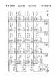
- the particular topology of the integrated circuitis not critical for purposes of the present invention. However, several important aspects of such an integrated circuit in accordance with a preferred embodiment of the invention are illustrated FIG. 3, showing a floor plan of the RCE core 300 of FIG. 2 .
- the RCE coreincludes a microprocessor portion 301 , an interface portion 310 , and an ACM portion 320 .
- the ACM portion 320is further subdivided into slices of reconfigurable logic.
- the slices of reconfigurable logicinclude control slices 323 a, 323 b, . . . , and corresponding datapath slices 327 a, 327 b, . . . .
- dataflows in a horizontal direction and control signals run from respective control slices to respective datapath slices in the vertical direction.
- An LSM array (also “sliceable”) 325may be located amidst the slices as shown, or may be located beside the slices.
- the microprocessor 302communicates with the slices through bus interfaces 319 a, 319 b, . . . , and communicates with the LSM array through a memory interface 311 .
- MACMedia Access Controller
- an external memory interface 306are also provided.
- each of the slices of reconfigurable logic, as well as the local store memory (LSM),include configuration memory for that portion.
- configuration memory for the blocks illustrated on the left-hand side of FIG. 3will most likely be merged together with those blocks in a “fabric,” i.e., a highly regular circuit structure.
- fabricsi.e., a highly regular circuit structure.
- Many different types of reconfigurable fabricsare well-known in the art.
- FIG. 4A block diagram of one possible implementation of the LSM is shown in FIG. 4 .
- the LSMis comprised of a tiled set of storage cells.
- the “M” cellsare nibble oriented storage structures that allow multi-port access in two dimensions.
- the “T” cellsare optionally used bit level cells associated with the M cells for either tag bit or error bit usage.
- the storage blockscan be further grouped into larger structures to support larger bit widths.
- arithmetic data operatorsare constructed sequentially, forming a row or path of operators.
- the resulting row of logic operators, multiplexers and registersis called a “datapath.”
- Datatravels down this path undergoing various operations and transformations.
- the ACM/LSM adaptive computation fabricis structured by using configuration data bits.
- the configuration bitsare organized in multiple planes of storage. Swapping configuration planes swaps the logic in the ACM. Data can be held in place and the operators reconfigured around the data as shown, for example in FIG. 5 .
- On a first cycledata passes from a first register 501 through a “cloud” of reconfigurable logic 503 to a second register 505 .
- the cloud of logicis then reconfigured, and one a subsequent cycle, the data passes back from the second register 505 through the cloud of logic 503 to the first register 501 .
- the equivalent of an arbitrarily long datapathmay be realized in ping-pong fashion.
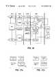
- the present ACMis a heterogeneous configurable fabric of control, datapath and memory partitions, including a fine-grained control structure that is used to control a coarse-grained datapath structure.
- the reconfigurable compute fabricmay consist of a number of tiled cells that extend in the X and Y coordinate system, including DPUs (Data Path Units) and the associated ICM (InterConnection Module) components.
- the DPUsprovide the data path functionality for the behavioral mapping and the ICMs define the bus oriented interconnection between the DPUs.
- the control portion and the LSM memory fabricare defined in a similar fashion.
- a fine-grained control structure fabric 610 a, 610 bconsists of tiled Boolean Logic Units (BLUs) 611 a, 611 b.
- the tiled BLU arrayinterfaces to a global signal control bus and CPU register control interface 609 .
- the global signal bus 609allows clock gating of registered variables or bidirectional steerage of data values.
- the BLUsare bit level oriented cells for orthogonal control of the ACM's datapath DPU partition slices 620 a, 620 b. This control can be in the form of cones of combinatorial logic or small state machines.
- the datapath partitionis a sliceable structure comprised of multiple bit, coarse-grained configurable datapath cells, DPUs (Datapath Program Units) 621 a, . . . , 621 b . . . , that efficiently support typical arithmetic and bit multiplexing operators.
- the DPUsoperate on data in 4 bit nibbles. This allows the datapath fabric to be implemented in a denser, coarse-grained silicon implementation, compared to current FPGA technology, which uses inefficient, bit-oriented logic elements (fine-grained).
- the coarser-grained aggregation of dataalso allows construction of high performance, long bit width arithmetic function modules such as multipliers and adders. Fewer bits of control for logic configuration are required, compared to conventional bit-oriented FPGA structures.
- Interconnection Modules 630 a, 630 bare used to communicate with the LSM storage mechanism for high bandwidth data traffic for queuing or loop processing.
- configuration memory planes underlying each of the various reconfigurable structuresare explicitly shown.
- This representationis a logical representation of the ACM and not necessarily a physical representation. Physically, the structures illustrated in three dimensions in FIG. 6 may be mapped to two dimensions.
- the LSMis realized in distributed fashion, e.g., as 4 ⁇ 4 blocks of memory interspersed with the DPUs. Dispersing the LSM relieves a possible memory bottleneck. Instead of accessing the LSM through the routing/memory interface, external system memory can be accessed through the routing/memory interface.
- DPUs and LSM blocksalternate in the vertical direction. That is, datapath slices alternate with LSM slices.
- DPUs and LSM blocksinstead alternate in the horizontal (dataflow) direction. This layout models typical algorithm flow of operator, storage, operator, storage in a pipelined implementation.
- DPUdigital signal processor
- FIG. 9A logic symbol for one possible DPU is shown in FIG. 9 .
- the DPUoperates as set forth in Table 1.
- FIG. 10An exemplary datapath circuit realized using such DPUs is shown in FIG. 10 .
- An important feature of the RCE coreis the ability to dynamically reconfigure the ACM on the fly in a very short amount of time--typically less than the amount of time required for a memory read operation in a conventional computer.
- the structure of the ACM/LSM fabricis specially adapted to enable this type of operation. More particularly, the ACM/LSM includes multiple logical memory planes, e.g., four memory planes, eight memory planes, etc. Any number of planes may be provided for (including numbers not powers of two).
- the fabricincludes control reconfigurable logic (C-RL) 1101 , datapath reconfigurable logic (D-RL) 1103 , and reconfigurable memory 1105 .
- C-RLcontrol reconfigurable logic
- D-RLdatapath reconfigurable logic
- reconfigurable memory 1105Associated with each of these structures is multiple planes of configuration storage, i.e, control configuration storage 1107 , datapath configuration storage 1109 and memory configuration storage 1111 .
- FIG. 12 aA particular embodiment of a portion of a multiple plane corresponding to a block of the ACM/LSM fabric is shown in FIG. 12 a.
- the multiple memory planesform in effect a memory plane stack 1200 .
- the top two planes 1206 , 1205 of the memory plane stackare configuration planes. Configuration data stored in these planes is applied to the reconfigurable logic.
- “function” configuration data and “wire” configuration datais stored in different planes.
- the bottom memory plane 1200 aprovides external access to the memory stack.
- Intermediate planesfunction, for example, as a configuration stack, storing configurations expected to be used by not presently active.
- memory plane 0is single port, for single-channel read and write between system memory and configuration storage.
- the remaining memory planesare dual port, having one read port and one write port. Dual port supports simultaneous loading and recirculation of configuration data with the local “stack.” If no data compression is used, then simultaneous real-time monitoring is possible, e.g., by writing out a “snapshot” of one or more planes of the stack.
- FIG. 12 bA group of corresponding memory cells, one cell from each plane of the memory stack, is shown in FIG. 12 b.
- the ports of all of the cellsare interconnected so as to allow an operation in which the contents of a cell within any plane may be read and then written to the corresponding cell of any other plane. For example, by activating the appropriate control signal, the contents of plane 4 may be read and written into plane 6. Such an operation may be accomplished, preferably, in a single clock cycle, or at most a few clock cycles.
- configuration datais loaded from external main memory into plane 0 of the memory stack in anticipation of its being transferred into a configuration plane.
- FIG. 12 cseparate “function” and “wire” stacks may be provided, as shown in FIG. 12 c. Using this arrangement, function and wire configurations may be changed simultaneously. Similarly, configuration stacks for configuration of control, datapath and memory may be combined (FIG. 12 d ) or separate (FIG. 12 e ).
- FIG. 13A schematic diagram of an alternative embodiment of a cell stack is shown in FIG. 13, showing a cross section of several configuration planes 1301 - 1304 and the lockable fabric-definition cell 1305 that produces a Fabric_Define_Data bit for a single bit location. These bits are aggregated in order to form sufficient bit numbers for functional cell type definition. For instance, a four bit grouping might designate between four to sixteen different cell type definitions.
- the other latch sites below the storage cellare for additional configuration plane data available for swapping as needed by functional scheduling requirements. These storage locations can be written and read to from a common configuration data bus structure.
- the Config_Read_Data and Config_Load_Data buses 1307 and 1309although shown as being separate, can be combined as a single bidirectional bus for wiring efficiency.
- the Swap_Read_Plane buffer 1311allows existing configuration plane data contents to be swapped among differing configuration planes on a selectable basis. For instance, the current operation plane of data can be loaded from configuration plane 1 to configuration plane 2 by the use of the Swap_Read_Plane buffer 1311 .
- the structure shown in FIG. 13is similar to a conventional SRAM memory structure which allows a dense VLSI circuitry implementation using standard memory compiler technology. This structure could also be implemented as a conventional dual port RAM structure (not shown) which would allow for concurrent operation of the write and read data operations.
- FIG. 12 bassumes separate configuration stacks for each configuration plane as described hereinafter. That is, the bit stack produces only a single Fabric_Define_Data bit instead of multiple fabric definition data bits as in FIG. 12 b.
- Data_Recirc_Read line 1313is also connected to data storage locations that are used for normal circuit register operation, then real time monitoring of device operations can be utilized by the operating system for applications such as RMON in internetworking application area or for real time debug capability.
- the RMON applicationbasically uses counter operation status from registers in order to determine system data operation flow characteristics.
- FIG. 14is a system level perspective of an access portion of the configurable ACM LSM, which provides the functionality necessary to configure an operable plane of logic.
- the logic shownis at a symbolic level of representation while the actual logic to perform the cell selection and address decode can vary according to techniques commonly used for address and data for SRAM structures.
- a set of X and Y decode latches with associated buffers 1401 , 1403drive decode enable signals into the tiled logic plane consisting of a replicated structure composed of NAND gates 1405 , 1407 and a configuration plane logic cell 1409 of the type described in relation to FIG. 14 .
- the combination X and Y decode structureenables arbitrary collections of cell sites to be addressed by the corresponding X and Y decode enables, which are shown NANDed together to provide row/column decode capability.
- the address bus 1411selects a particular configuration plane and is globally broadcast into the slice of the larger array to be programmed for either read or write of configuration data.
- the configuration data busin not shown for simplicity.
- the global address bus 1411is decoded at each cell by the use of local cell decode logic (NAND gates 1405 ).
- the global address busmay be implemented in terms of straight-line, single-bit word lines.
- FIG. 14allows programming compression to be accomplished by running a compression program on the configuration map to find the commonly repeating structures so that they may be written simultaneously. This measure will significantly reduce both the size of the data file and the corresponding load time, since most of the like datapath elements will be repeating both horizontally and vertically.
- Configuration patternssuch as those shown in FIG. 15 a through FIG. 15 f.
- the cells that correspond to a “maximal function” having highest utilizationare globally selected by the X/Y decode latches for maximal coverage, and a configuration plane address is broadcast, designating a particular configuration plane layer.
- a global data bus(not shown) then loads a data value that corresponds to a given logic operator or wiring configuration. The next most commonly used function may then be loaded in a like process.
- next configuration mapping of commonly used cell typescan in fact over-write cell locations from the previous load cell type operation. That is, successive cell type load operations can supersede previous cell content loading.
- This method of loadingallows the maximal functions to be stitched into the configuration fabric as needed in arbitrary cell locations.
- the ordering of cell types by usage for a given configuration planeallows the compression of information content such that individual addressing schemes for each cell location are not necessary.
- the foregoing discussionhas focused on the reconfigurable ACM/LSM fabric. The remainder of the discussion will focus on the interface between the fabric and the microprocessor.
- the microprocessorfollows a standard RISC architecture and has multiple coprocessor and special instructions that may be used to interface with the reconfigurable logic. If the instructions are not used, then the configuration programming automatically adds default tie-off conditions (for cells that are not used or to safely configure routing to prevent interference of operations).
- the microprocessorinterfaces with the reconfigurable logic through some or all of the following mechanisms:
- the reconfigurable memory or logic planescan be accessed by writing to or reading from a defined address space via the system bus. This operation appears as if it were a regular memory access.
- the RISC architecturespecial instructions for loading coprocessor registers and turning control over to a coprocessor.
- the coprocessorin this case the ACM/LSM
- the processorcan load the contents of the coprocessor interface registers back into the processor.
- FIG. 16illustrating coupling of the processor core with the reconfigurable fabric.
- the processor coreis realized as a four-stage pipeline including stages 1610 , 1620 , 1630 and 1640 (the execution stage).
- stages 1610 , 1620 , 1630 and 1640the execution stage.
- an ALU and the ACMare tightly coupled.
- both the ALU and the ACMreceive operational data from a register file in the stage 1630 .
- a mappingis performed between a smaller number of registers (e.g., 32) within the register file to a potentially much larger number of registers within the ACM.
- Special register-register or register-memory instructionscause two or more words to be loaded into a register at the boundary of the bus.
- a mechanismis provided for stalling loading of results computed in the ACM and LSM fabric into the CPU register set, if necessary, to preserve sequential program execution integrity.
- the stall mechanismmay take the form of a flag, a dedicated signal line, etc.
- the results of the operationare placed within a set of special instruction registers. Any request to read the contents of a special instruction register before the stall for those registers has been cleared stalls that read instruction.
- the coprocessor or special instruction registersmay be read or written by either the processor or the ACM.
- a clock offset from the processor clockmay be provided to guarantee alternating read-write cycle operation if the ACM can keep up with the processor.
- Load instructionsare used to load a plane within a block.
- the ability to swap planesis available both to the microprocessor and to the reconfigurable logic blocks. More than one function can be mapped onto a plane within a block, or a single functions can take up more than one block or plane. Possible configurations are shown in FIG. 17 a and FIG. 17 b.
- the function map tableprovides the module address for the function.
- the module addressis the address in main memory of the blocks, in compressed format, to be loaded.
- the function tablealso contains Plane Utilization Bits (PUBs), along with lock and swap bits for the function.
- POBsPlane Utilization Bits
- the plane utilization bitsare assigned based on execution ordering of functions that are mapped to modules in hardware for sequential program execution.
- the Load functionissues a soft interrupt which is handled by an on-chip “mini operating system” in a manner similar to a supervisor call.
- the old functions in the tableare cleared for the target planes, and the planes are loaded via move instructions which use DMA transfers, in a manner similar to an interrupt driven I/O operation. While the DMA transfers are occurring, the processor returns to execute its normal instruction stream. An interrupt signalling completion of the transfer of the planes will re-enter the “driver” code which will update the function map table. If the function is already loaded, then the Load instruction returns without loading. If the module address does not exist then the operation aborts with an error exception.
- the Invoke commandcopies the contents of one plane to another.
- block configuration wordsare maintained for each block in the ACM, including, for each block, a Routing Plane word and a Function Plane word.
- Run, Lock and Swap bitsindicate the status of the current effective configurations within each block.
- a “From Plane” fieldmay be used to swap a function back to a previous plane.
- the information in the block configuration wordsis used to determined how to handle the Execute instruction.
- the Execute instructionis decoded by the control logic interface to the reconfigurable logic. Either the function is resident, in which case it is executed with Run set to 1 on the appropriate planes and blocks, or it is not, in which case a soft interrupt is executed which branches the processor into an exception handling routine with the return address at the Execute command, allowing the instruction to be reissued when the function is loaded.
- the exception handling routineissues one or more Invoke commands with the appropriate parameters, after determining if the current functions are locked or swappable as specified in the appropriate block configuration bits. If the block are current executing another function, Run is set to 1. If the Swap bit is 1, then functions is swappable. If the Lock bit is set to 1, then the current plane is locked.
- One suitable exception handling routineis described by the pseudocode of listing FIG. 19 .
- the effect of the exception routineis to re-execute the routine after it has been loaded or swapped in, or to skip the instruction. Note that if the currently executing function is not locked or swappable, it may be aborted.
- the result of the foregoing approachis to allow the software to improve the run time by early loading and invoking of the functions, while always executing the functions, if at all possible, whether they have been previously loaded or not.
Landscapes
- Engineering & Computer Science (AREA)
- Theoretical Computer Science (AREA)
- Software Systems (AREA)
- Physics & Mathematics (AREA)
- General Engineering & Computer Science (AREA)
- General Physics & Mathematics (AREA)
- Computer Hardware Design (AREA)
- Logic Circuits (AREA)
Abstract
Description
| TABLE 1 | ||
| OP CODE | OPERATION | COMMENT |
| 0000 | NOP | Passes A and B through to the higher |
| and lower output bits, respectively | ||
| 0001 | SUB | Cin must be 1 |
| 0010 | AND | |
| 0011 | MUL | May increment as well if Cin = 1 |
| 0100 | OR | |
| 0101 | INC | Cin must be 1; increments A and B |
| together as a four-bit number | ||
| 0110 | XOR | |
| 0111 | ADD | |
| 1000 | SWAP | Passes B and A through to the higher |
| and lower output bits, respectively | ||
| 1001 | SHIFT4 | Works on all four input bits, not just |
| two | ||
| 1010 | ROT1 | Works on all four input bits, not just |
| two | ||
| 1011 | SHIFT1 | Works on all four input bits, not just |
| two | ||
| 1100 | ROT2 | Works on all four input bits, not just |
| two | ||
| 1101 | SHIFT2 | Works on all four input bits, not just |
| two | ||
| 1110 | ||
| 1111 | SHIFT3 | |
Claims (29)
Priority Applications (1)
| Application Number | Priority Date | Filing Date | Title |
|---|---|---|---|
| US09/446,762US6282627B1 (en) | 1998-06-29 | 1998-06-29 | Integrated processor and programmable data path chip for reconfigurable computing |
Applications Claiming Priority (2)
| Application Number | Priority Date | Filing Date | Title |
|---|---|---|---|
| PCT/US1998/013565WO1999000739A1 (en) | 1997-06-27 | 1998-06-29 | An integrated processor and programmable data path chip for reconfigurable computing |
| US09/446,762US6282627B1 (en) | 1998-06-29 | 1998-06-29 | Integrated processor and programmable data path chip for reconfigurable computing |
Publications (1)
| Publication Number | Publication Date |
|---|---|
| US6282627B1true US6282627B1 (en) | 2001-08-28 |
Family
ID=23773746
Family Applications (1)
| Application Number | Title | Priority Date | Filing Date |
|---|---|---|---|
| US09/446,762Expired - LifetimeUS6282627B1 (en) | 1998-06-29 | 1998-06-29 | Integrated processor and programmable data path chip for reconfigurable computing |
Country Status (1)
| Country | Link |
|---|---|
| US (1) | US6282627B1 (en) |
Cited By (174)
| Publication number | Priority date | Publication date | Assignee | Title |
|---|---|---|---|---|
| US6338106B1 (en) | 1996-12-20 | 2002-01-08 | Pact Gmbh | I/O and memory bus system for DFPS and units with two or multi-dimensional programmable cell architectures |
| US20020100032A1 (en)* | 2000-08-07 | 2002-07-25 | Paul Metzgen | Software-to-hardware compiler |
| US20020138716A1 (en)* | 2001-03-22 | 2002-09-26 | Quicksilver Technology, Inc. | Adaptive integrated circuitry with heterogeneous and reconfigurable matrices of diverse and adaptive computational units having fixed, application specific computational elements |
| US6467009B1 (en)* | 1998-10-14 | 2002-10-15 | Triscend Corporation | Configurable processor system unit |
| US6477643B1 (en) | 1996-12-27 | 2002-11-05 | Pact Gmbh | Process for automatic dynamic reloading of data flow processors (dfps) and units with two-or-three-dimensional programmable cell architectures (fpgas, dpgas, and the like) |
| US20030020082A1 (en)* | 2001-07-25 | 2003-01-30 | Motorola, Inc. | Structure and method for fabricating semiconductor structures and devices for optical switching |
| US6522167B1 (en) | 2001-01-09 | 2003-02-18 | Xilinx, Inc. | User configurable on-chip memory system |
| US6526520B1 (en) | 1997-02-08 | 2003-02-25 | Pact Gmbh | Method of self-synchronization of configurable elements of a programmable unit |
| US20030056202A1 (en)* | 2001-08-16 | 2003-03-20 | Frank May | Method for translating programs for reconfigurable architectures |
| US6542998B1 (en) | 1997-02-08 | 2003-04-01 | Pact Gmbh | Method of self-synchronization of configurable elements of a programmable module |
| US6557092B1 (en)* | 1999-03-29 | 2003-04-29 | Greg S. Callen | Programmable ALU |
| US20030105949A1 (en)* | 2001-11-30 | 2003-06-05 | Quicksilver Technology, Inc. | Apparatus, method, system and executable module for configuration and operation of adaptive integrated circuitry having fixed, application specific computational elements |
| US20030102889A1 (en)* | 2001-11-30 | 2003-06-05 | Master Paul L. | Apparatus, system and method for configuration of adaptive integrated circuitry having fixed, application specific computational elements |
| US20030126450A1 (en)* | 2001-12-27 | 2003-07-03 | Quicksilver Technology, Inc. | Apparatus, method and system for generating a unique hardware adaptation inseparable from correspondingly unique content |
| US20030154357A1 (en)* | 2001-03-22 | 2003-08-14 | Quicksilver Technology, Inc. | Adaptive integrated circuitry with heterogeneous and reconfigurable matrices of diverse and adaptive computational units having fixed, application specific computational elements |
| US20030163798A1 (en)* | 2002-02-22 | 2003-08-28 | Xilinx, Inc. | Method and system for integrating cores in FPGA-based system-on-chip (SoC) |
| US6617877B1 (en) | 2002-03-01 | 2003-09-09 | Xilinx, Inc. | Variable data width operation in multi-gigabit transceivers on a programmable logic device |
| US20030190910A1 (en)* | 2001-05-08 | 2003-10-09 | Scheuermann W. James | Method and system for reconfigurable channel coding |
| US20030192032A1 (en)* | 1998-02-17 | 2003-10-09 | National Instruments Corporation | System and method for debugging a software program |
| US6647511B1 (en)* | 1998-09-17 | 2003-11-11 | Texas Instruments Incorporated | Reconfigurable datapath for processor debug functions |
| US6658564B1 (en)* | 1998-11-20 | 2003-12-02 | Altera Corporation | Reconfigurable programmable logic device computer system |
| US6662285B1 (en) | 2001-01-09 | 2003-12-09 | Xilinx, Inc. | User configurable memory system having local and global memory blocks |
| US6687788B2 (en) | 1998-02-25 | 2004-02-03 | Pact Xpp Technologies Ag | Method of hierarchical caching of configuration data having dataflow processors and modules having two-or multidimensional programmable cell structure (FPGAs, DPGAs , etc.) |
| US6693452B1 (en) | 2002-02-25 | 2004-02-17 | Xilinx, Inc. | Floor planning for programmable gate array having embedded fixed logic circuitry |
| US6697979B1 (en) | 1997-12-22 | 2004-02-24 | Pact Xpp Technologies Ag | Method of repairing integrated circuits |
| US6721840B1 (en) | 2000-08-18 | 2004-04-13 | Triscend Corporation | Method and system for interfacing an integrated circuit to synchronous dynamic memory and static memory |
| US6735756B1 (en) | 2002-02-22 | 2004-05-11 | Xilinx, Inc. | Method and architecture for dynamic device drivers |
| US6754882B1 (en) | 2002-02-22 | 2004-06-22 | Xilinx, Inc. | Method and system for creating a customized support package for an FPGA-based system-on-chip (SoC) |
| US6760898B1 (en) | 2002-02-22 | 2004-07-06 | Xilinx, Inc. | Method and system for inserting probe points in FPGA-based system-on-chip (SoC) |
| US20040130927A1 (en)* | 2002-10-31 | 2004-07-08 | Lockheed Martin Corporation | Pipeline accelerator having multiple pipeline units and related computing machine and method |
| US20040132479A1 (en)* | 2001-12-05 | 2004-07-08 | Rubin Owen Robert | Consumer product distribution in the embedded system market |
| US20040143724A1 (en)* | 2002-09-30 | 2004-07-22 | Quicksilver Technology, Inc. | System and method using embedded microprocessor as a node in an adaptable computing machine |
| US6772405B1 (en) | 2002-06-13 | 2004-08-03 | Xilinx, Inc. | Insertable block tile for interconnecting to a device embedded in an integrated circuit |
| US6781407B2 (en) | 2002-01-09 | 2004-08-24 | Xilinx, Inc. | FPGA and embedded circuitry initialization and processing |
| US20040181614A1 (en)* | 2001-03-22 | 2004-09-16 | Quicksilver Technology, Inc. | Input/output controller node in an adaptable computing environment |
| US6798239B2 (en) | 2001-09-28 | 2004-09-28 | Xilinx, Inc. | Programmable gate array having interconnecting logic to support embedded fixed logic circuitry |
| US20040194952A1 (en)* | 2002-08-06 | 2004-10-07 | Hector Maiolo | Oil extraction equipment |
| US6810458B1 (en) | 2002-03-01 | 2004-10-26 | Xilinx, Inc. | Method and circuit for hot swap protection |
| US6820248B1 (en) | 2002-02-14 | 2004-11-16 | Xilinx, Inc. | Method and apparatus for routing interconnects to devices with dissimilar pitches |
| US20040234017A1 (en)* | 2003-05-20 | 2004-11-25 | Andrew Tomerlin | Delay line based multiple frequency generator circuits for CDMA processing |
| US6826674B1 (en)* | 1999-08-30 | 2004-11-30 | Ip Flex, Inc. | Program product and data processor |
| US6839874B1 (en) | 2002-02-28 | 2005-01-04 | Xilinx, Inc. | Method and apparatus for testing an embedded device |
| US6851047B1 (en) | 1999-10-15 | 2005-02-01 | Xilinx, Inc. | Configuration in a configurable system on a chip |
| US6859869B1 (en) | 1995-11-17 | 2005-02-22 | Pact Xpp Technologies Ag | Data processing system |
| US20050040850A1 (en)* | 2001-09-28 | 2005-02-24 | Xilinx, Inc. | Programmable gate array and embedded circuitry initialization and processing |
| US20050058186A1 (en)* | 2003-09-11 | 2005-03-17 | Xilinx, Inc. | Channel bonding of a plurality of multi-gigabit transceivers |
| US20050063455A1 (en)* | 2003-04-22 | 2005-03-24 | Tomerlin Andrew T. | Multiple user reconfigurable CDMA processor |
| WO2004049175A3 (en)* | 2002-11-22 | 2005-04-21 | Quicksilver Tech Inc | External memory controller node |
| US6886092B1 (en) | 2001-11-19 | 2005-04-26 | Xilinx, Inc. | Custom code processing in PGA by providing instructions from fixed logic processor portion to programmable dedicated processor portion |
| US20050125760A1 (en)* | 2003-12-04 | 2005-06-09 | International Business Machines Corporation | Data processing in digital systems |
| US20050144212A1 (en)* | 2003-12-29 | 2005-06-30 | Xilinx, Inc. | Programmable logic device with cascading DSP slices |
| US20050144216A1 (en)* | 2003-12-29 | 2005-06-30 | Xilinx, Inc. | Arithmetic circuit with multiplexed addend inputs |
| US20050144210A1 (en)* | 2003-12-29 | 2005-06-30 | Xilinx, Inc. | Programmable logic device with dynamic DSP architecture |
| US20050144215A1 (en)* | 2003-12-29 | 2005-06-30 | Xilinx, Inc. | Applications of cascading DSP slices |
| US20050144211A1 (en)* | 2003-12-29 | 2005-06-30 | Xilinx, Inc. | Programmable logic device with pipelined DSP slices |
| WO2005010632A3 (en)* | 2003-06-17 | 2005-07-07 | Pact Xpp Technologies Ag | Data processing device and method |
| US20050151562A1 (en)* | 2002-12-31 | 2005-07-14 | Tsvika Kurts | Apparatus and method for bus signal termination compensation during detected quiet cycle |
| US6920551B1 (en) | 2001-03-08 | 2005-07-19 | Xilinx, Inc. | Configurable processor system |
| US20050168260A1 (en)* | 2004-01-29 | 2005-08-04 | Tomerlin Andrew T. | Configurable delay line circuit |
| US6934922B1 (en) | 2002-02-27 | 2005-08-23 | Xilinx, Inc. | Timing performance analysis |
| US6944836B1 (en) | 2002-11-15 | 2005-09-13 | Xilinx, Inc. | Structures and methods for testing programmable logic devices having mixed-fabric architectures |
| WO2005071850A3 (en)* | 2004-01-22 | 2005-10-13 | Koninkl Philips Electronics Nv | A dynamically reconfigurable signal processing apparatus and method for use in a high speed digital communication system |
| US6961919B1 (en) | 2002-03-04 | 2005-11-01 | Xilinx, Inc. | Method of designing integrated circuit having both configurable and fixed logic circuitry |
| US6970013B1 (en) | 2002-03-01 | 2005-11-29 | Xilinx, Inc | Variable data width converter |
| US6973405B1 (en) | 2002-05-22 | 2005-12-06 | Xilinx, Inc. | Programmable interactive verification agent |
| US6976160B1 (en) | 2002-02-22 | 2005-12-13 | Xilinx, Inc. | Method and system for controlling default values of flip-flops in PGA/ASIC-based designs |
| US6983405B1 (en) | 2001-11-16 | 2006-01-03 | Xilinx, Inc., | Method and apparatus for testing circuitry embedded within a field programmable gate array |
| US20060015701A1 (en)* | 2002-11-01 | 2006-01-19 | Quicksilver Technology, Inc. | Arithmetic node including general digital signal processing functions for an adaptive computing machine |
| US6990555B2 (en) | 2001-01-09 | 2006-01-24 | Pact Xpp Technologies Ag | Method of hierarchical caching of configuration data having dataflow processors and modules having two- or multidimensional programmable cell structure (FPGAs, DPGAs, etc.) |
| US6996758B1 (en) | 2001-11-16 | 2006-02-07 | Xilinx, Inc. | Apparatus for testing an interconnecting logic fabric |
| US7003660B2 (en) | 2000-06-13 | 2006-02-21 | Pact Xpp Technologies Ag | Pipeline configuration unit protocols and communication |
| US7007121B1 (en) | 2002-02-27 | 2006-02-28 | Xilinx, Inc. | Method and apparatus for synchronized buses |
| US7010667B2 (en)* | 1997-02-11 | 2006-03-07 | Pact Xpp Technologies Ag | Internal bus system for DFPS and units with two- or multi-dimensional programmable cell architectures, for managing large volumes of data with a high interconnection complexity |
| US20060085781A1 (en)* | 2004-10-01 | 2006-04-20 | Lockheed Martin Corporation | Library for computer-based tool and related system and method |
| US20060087342A1 (en)* | 2004-10-27 | 2006-04-27 | Manuj Ayodhyawasi | Interconnect structure and method in programmable devices |
| US20060109842A1 (en)* | 2002-08-29 | 2006-05-25 | Thiele Matthew J | Reconfigurable compute engine interconnect fabric |
| US7058920B2 (en) | 2001-05-06 | 2006-06-06 | Altera Corporation | Methods for designing PLD architectures for flexible placement of IP function blocks |
| US7058921B1 (en) | 2002-02-22 | 2006-06-06 | Xilinx, Inc. | Method and system for resource allocation in FPGA-based system-on-chip (SoC) |
| US7076595B1 (en) | 2001-05-18 | 2006-07-11 | Xilinx, Inc. | Programmable logic device including programmable interface core and central processing unit |
| US7085973B1 (en) | 2002-07-09 | 2006-08-01 | Xilinx, Inc. | Testing address lines of a memory controller |
| US7088767B1 (en) | 2002-03-01 | 2006-08-08 | Xilinx, Inc. | Method and apparatus for operating a transceiver in different data rates |
| US7092865B1 (en) | 2002-09-10 | 2006-08-15 | Xilinx, Inc. | Method and apparatus for timing modeling |
| US20060190516A1 (en)* | 2003-12-29 | 2006-08-24 | Xilinx, Inc. | Digital signal processing element having an arithmetic logic unit |
| US7099426B1 (en) | 2002-09-03 | 2006-08-29 | Xilinx, Inc. | Flexible channel bonding and clock correction operations on a multi-block data path |
| US20060206557A1 (en)* | 2003-12-29 | 2006-09-14 | Xilinx, Inc. | Arithmetic logic unit circuit |
| US7111217B1 (en) | 2002-02-28 | 2006-09-19 | Xilinx, Inc. | Method and system for flexibly nesting JTAG TAP controllers for FPGA-based system-on-chip (SoC) |
| US7111220B1 (en) | 2002-03-01 | 2006-09-19 | Xilinx, Inc. | Network physical layer with embedded multi-standard CRC generator |
| US20060212499A1 (en)* | 2003-12-29 | 2006-09-21 | Xilinx, Inc. | Digital signal processing block having a wide multiplexer |
| US7114069B2 (en) | 2003-04-22 | 2006-09-26 | Motorola, Inc. | Reconfigurable processing circuit including a delay locked loop multiple frequency generator for generating a plurality of clock signals which are configured in frequency by a control processor |
| US7124382B1 (en) | 2002-03-01 | 2006-10-17 | Xilinx, Inc. | Method and apparatus for rule file generation |
| US20060265571A1 (en)* | 2003-03-05 | 2006-11-23 | Thomas Bosch | Processor with different types of control units for jointly used resources |
| US20060288070A1 (en)* | 2003-12-29 | 2006-12-21 | Xilinx, Inc. | Digital signal processing circuit having a pattern circuit for determining termination conditions |
| US7174443B1 (en) | 1996-12-20 | 2007-02-06 | Pact Xpp Technologies Ag | Run-time reconfiguration method for programmable units |
| US7187709B1 (en) | 2002-03-01 | 2007-03-06 | Xilinx, Inc. | High speed configurable transceiver architecture |
| US7237087B2 (en) | 1996-12-09 | 2007-06-26 | Pact Xpp Technologies Ag | Reconfigurable multidimensional array processor allowing runtime reconfiguration of selected individual array cells |
| US7266725B2 (en) | 2001-09-03 | 2007-09-04 | Pact Xpp Technologies Ag | Method for debugging reconfigurable architectures |
| US7343594B1 (en) | 2000-08-07 | 2008-03-11 | Altera Corporation | Software-to-hardware compiler with symbol set inference analysis |
| US20080094106A1 (en)* | 2006-10-19 | 2008-04-24 | David Glen Edwards | Apparatus for configuring I/O signal levels of interfacing logic circuits |
| US7382823B1 (en) | 2002-02-22 | 2008-06-03 | Xilinx, Inc. | Channel bonding control logic architecture |
| US7394284B2 (en) | 2002-09-06 | 2008-07-01 | Pact Xpp Technologies Ag | Reconfigurable sequencer structure |
| CN100412789C (en)* | 2004-06-25 | 2008-08-20 | 富士通株式会社 | Reconfigurable Processors and Semiconductor Devices |
| US7433909B2 (en) | 2002-06-25 | 2008-10-07 | Nvidia Corporation | Processing architecture for a reconfigurable arithmetic node |
| US7434191B2 (en) | 2001-09-03 | 2008-10-07 | Pact Xpp Technologies Ag | Router |
| US7444531B2 (en) | 2001-03-05 | 2008-10-28 | Pact Xpp Technologies Ag | Methods and devices for treating and processing data |
| US7478031B2 (en) | 2002-11-07 | 2009-01-13 | Qst Holdings, Llc | Method, system and program for developing and scheduling adaptive integrated circuity and corresponding control or configuration information |
| US7489779B2 (en) | 2001-03-22 | 2009-02-10 | Qstholdings, Llc | Hardware implementation of the secure hash standard |
| US7493375B2 (en) | 2002-04-29 | 2009-02-17 | Qst Holding, Llc | Storage and delivery of device features |
| US7512173B2 (en) | 2001-12-12 | 2009-03-31 | Qst Holdings, Llc | Low I/O bandwidth method and system for implementing detection and identification of scrambling codes |
| US7577799B1 (en) | 2003-08-19 | 2009-08-18 | Nvidia Corporation | Asynchronous, independent and multiple process shared memory system in an adaptive computing architecture |
| US7577822B2 (en) | 2001-12-14 | 2009-08-18 | Pact Xpp Technologies Ag | Parallel task operation in processor and reconfigurable coprocessor configured based on information in link list including termination information for synchronization |
| US7581076B2 (en) | 2001-03-05 | 2009-08-25 | Pact Xpp Technologies Ag | Methods and devices for treating and/or processing data |
| US7595659B2 (en) | 2000-10-09 | 2009-09-29 | Pact Xpp Technologies Ag | Logic cell array and bus system |
| US7602740B2 (en) | 2001-12-10 | 2009-10-13 | Qst Holdings, Inc. | System for adapting device standards after manufacture |
| US7606943B2 (en) | 2002-10-28 | 2009-10-20 | Qst Holdings, Llc | Adaptable datapath for a digital processing system |
| US7609297B2 (en) | 2003-06-25 | 2009-10-27 | Qst Holdings, Inc. | Configurable hardware based digital imaging apparatus |
| US7620678B1 (en) | 2002-06-12 | 2009-11-17 | Nvidia Corporation | Method and system for reducing the time-to-market concerns for embedded system design |
| US7620097B2 (en) | 2001-03-22 | 2009-11-17 | Qst Holdings, Llc | Communications module, device, and method for implementing a system acquisition function |
| US7650448B2 (en) | 1996-12-20 | 2010-01-19 | Pact Xpp Technologies Ag | I/O and memory bus system for DFPS and units with two- or multi-dimensional programmable cell architectures |
| US7653710B2 (en) | 2002-06-25 | 2010-01-26 | Qst Holdings, Llc. | Hardware task manager |
| US7657861B2 (en) | 2002-08-07 | 2010-02-02 | Pact Xpp Technologies Ag | Method and device for processing data |
| US7657877B2 (en) | 2001-06-20 | 2010-02-02 | Pact Xpp Technologies Ag | Method for processing data |
| US20100031231A1 (en)* | 2008-07-30 | 2010-02-04 | Kosta Ilic | Testing a Graphical Program Intended for a Programmable Hardware Element |
| US7660984B1 (en) | 2003-05-13 | 2010-02-09 | Quicksilver Technology | Method and system for achieving individualized protected space in an operating system |
| AU2003287317B2 (en)* | 2002-10-31 | 2010-03-11 | Lockheed Martin Corporation | Pipeline accelerator having multiple pipeline units and related computing machine and method |
| US7712140B2 (en) | 2003-08-04 | 2010-05-04 | Lsi Corporation | 3-prong security/reliability/real-time distributed architecture of information handling system |
| US20100159910A1 (en)* | 2002-01-04 | 2010-06-24 | Qst Holdings, Inc. | Apparatus and method for adaptive multimedia reception and transmission in communication environments |
| US7752419B1 (en) | 2001-03-22 | 2010-07-06 | Qst Holdings, Llc | Method and system for managing hardware resources to implement system functions using an adaptive computing architecture |
| US7802108B1 (en) | 2002-07-18 | 2010-09-21 | Nvidia Corporation | Secure storage of program code for an embedded system |
| US7822881B2 (en) | 1996-12-27 | 2010-10-26 | Martin Vorbach | Process for automatic dynamic reloading of data flow processors (DFPs) and units with two- or three-dimensional programmable cell architectures (FPGAs, DPGAs, and the like) |
| US7840627B2 (en) | 2003-12-29 | 2010-11-23 | Xilinx, Inc. | Digital signal processing circuit having input register blocks |
| US7844796B2 (en) | 2001-03-05 | 2010-11-30 | Martin Vorbach | Data processing device and method |
| US7844653B2 (en) | 2003-12-29 | 2010-11-30 | Xilinx, Inc. | Digital signal processing circuit having a pre-adder circuit |
| US7849119B2 (en) | 2003-12-29 | 2010-12-07 | Xilinx, Inc. | Digital signal processing circuit having a pattern detector circuit |
| US7853632B2 (en) | 2003-12-29 | 2010-12-14 | Xilinx, Inc. | Architectural floorplan for a digital signal processing circuit |
| US7853634B2 (en) | 2003-12-29 | 2010-12-14 | Xilinx, Inc. | Digital signal processing circuit having a SIMD circuit |
| US7853636B2 (en) | 2003-12-29 | 2010-12-14 | Xilinx, Inc. | Digital signal processing circuit having a pattern detector circuit for convergent rounding |
| US7865847B2 (en) | 2002-05-13 | 2011-01-04 | Qst Holdings, Inc. | Method and system for creating and programming an adaptive computing engine |
| US7870182B2 (en) | 2003-12-29 | 2011-01-11 | Xilinx Inc. | Digital signal processing circuit having an adder circuit with carry-outs |
| US7937591B1 (en) | 2002-10-25 | 2011-05-03 | Qst Holdings, Llc | Method and system for providing a device which can be adapted on an ongoing basis |
| US7987065B1 (en) | 2007-04-17 | 2011-07-26 | Nvidia Corporation | Automatic quality testing of multimedia rendering by software drivers |
| US7996827B2 (en) | 2001-08-16 | 2011-08-09 | Martin Vorbach | Method for the translation of programs for reconfigurable architectures |
| USRE42743E1 (en) | 2001-11-28 | 2011-09-27 | Qst Holdings, Llc | System for authorizing functionality in adaptable hardware devices |
| US8058899B2 (en) | 2000-10-06 | 2011-11-15 | Martin Vorbach | Logic cell array and bus system |
| US8108656B2 (en) | 2002-08-29 | 2012-01-31 | Qst Holdings, Llc | Task definition for specifying resource requirements |
| US20120030451A1 (en)* | 2010-07-28 | 2012-02-02 | Broadcom Corporation | Parallel and long adaptive instruction set architecture |
| US8127061B2 (en) | 2002-02-18 | 2012-02-28 | Martin Vorbach | Bus systems and reconfiguration methods |
| US8156284B2 (en) | 2002-08-07 | 2012-04-10 | Martin Vorbach | Data processing method and device |
| US8230411B1 (en) | 1999-06-10 | 2012-07-24 | Martin Vorbach | Method for interleaving a program over a plurality of cells |
| US8250503B2 (en) | 2006-01-18 | 2012-08-21 | Martin Vorbach | Hardware definition method including determining whether to implement a function as hardware or software |
| US8276135B2 (en) | 2002-11-07 | 2012-09-25 | Qst Holdings Llc | Profiling of software and circuit designs utilizing data operation analyses |
| US8281108B2 (en) | 2002-01-19 | 2012-10-02 | Martin Vorbach | Reconfigurable general purpose processor having time restricted configurations |
| US8296764B2 (en) | 2003-08-14 | 2012-10-23 | Nvidia Corporation | Internal synchronization control for adaptive integrated circuitry |
| US8479133B2 (en) | 2009-01-27 | 2013-07-02 | Xilinx, Inc. | Method of and circuit for implementing a filter in an integrated circuit |
| US8533431B2 (en) | 2001-03-22 | 2013-09-10 | Altera Corporation | Adaptive integrated circuitry with heterogeneous and reconfigurable matrices of diverse and adaptive computational units having fixed, application specific computational elements |
| US8543635B2 (en) | 2009-01-27 | 2013-09-24 | Xilinx, Inc. | Digital signal processing block with preadder stage |
| US8589935B2 (en) | 2007-05-08 | 2013-11-19 | L-3 Communications Corporation | Heterogeneous reconfigurable agent compute engine (HRACE) |
| US8686475B2 (en) | 2001-09-19 | 2014-04-01 | Pact Xpp Technologies Ag | Reconfigurable elements |
| US8686549B2 (en) | 2001-09-03 | 2014-04-01 | Martin Vorbach | Reconfigurable elements |
| US8804452B2 (en) | 2012-07-31 | 2014-08-12 | Micron Technology, Inc. | Data interleaving module |
| US8812820B2 (en) | 2003-08-28 | 2014-08-19 | Pact Xpp Technologies Ag | Data processing device and method |
| US8914590B2 (en) | 2002-08-07 | 2014-12-16 | Pact Xpp Technologies Ag | Data processing method and device |
| US8959469B2 (en) | 2012-02-09 | 2015-02-17 | Altera Corporation | Configuring a programmable device using high-level language |
| WO2015063466A1 (en) | 2013-10-31 | 2015-05-07 | Silicon Tailor Limited | Pipelined configurable processor |
| US9037807B2 (en) | 2001-03-05 | 2015-05-19 | Pact Xpp Technologies Ag | Processor arrangement on a chip including data processing, memory, and interface elements |
| US20160180896A1 (en)* | 2014-12-23 | 2016-06-23 | Arm Limited | Memory with multiple write ports |
| US9477999B2 (en) | 2013-09-20 | 2016-10-25 | The Board Of Trustees Of The Leland Stanford Junior University | Low power programmable image processor |
| US20170083313A1 (en)* | 2015-09-22 | 2017-03-23 | Qualcomm Incorporated | CONFIGURING COARSE-GRAINED RECONFIGURABLE ARRAYS (CGRAs) FOR DATAFLOW INSTRUCTION BLOCK EXECUTION IN BLOCK-BASED DATAFLOW INSTRUCTION SET ARCHITECTURES (ISAs) |
| RU174347U1 (en)* | 2017-05-18 | 2017-10-11 | Федеральное государственное унитарное предприятие "Научно-исследовательский институт "Квант" | COMPUTER MODULE |
| CN107341133A (en)* | 2017-06-24 | 2017-11-10 | 中国人民解放军信息工程大学 | The dispatching method of Reconfigurable Computation structure based on Arbitrary Dimensions LU Decomposition |
| US9996568B2 (en) | 2013-12-31 | 2018-06-12 | International Business Machines Corporation | Index maintenance based on a comparison of rebuild vs. update |
| RU2686004C1 (en)* | 2018-07-26 | 2019-04-23 | Федеральное государственное унитарное предприятие "Научно-исследовательский институт "Квант" | Computing module |
| US11055103B2 (en) | 2010-01-21 | 2021-07-06 | Cornami, Inc. | Method and apparatus for a multi-core system for implementing stream-based computations having inputs from multiple streams |
| US20230229407A1 (en)* | 2022-01-20 | 2023-07-20 | SambaNova Systems, Inc. | Compiler for a Fracturable Data Path in a Reconfigurable Data Processor |
| US12314754B2 (en) | 2022-08-23 | 2025-05-27 | SambaNova Systems, Inc. | Multiple contexts for a compute unit in a reconfigurable data processor |
Citations (14)
| Publication number | Priority date | Publication date | Assignee | Title |
|---|---|---|---|---|
| US5500609A (en) | 1992-11-05 | 1996-03-19 | Xilinx, Inc. | Wildcard addressing structure for configurable cellular array |
| US5535342A (en) | 1992-11-05 | 1996-07-09 | Giga Operations Corporation | Pld connector for module having configuration of either first PLD or second PLD and reconfigurable bus for communication of two different bus protocols |
| US5535406A (en) | 1993-12-29 | 1996-07-09 | Kolchinsky; Alexander | Virtual processor module including a reconfigurable programmable matrix |
| US5583749A (en) | 1994-11-30 | 1996-12-10 | Altera Corporation | Baseboard and daughtercard apparatus for reconfigurable computing systems |
| US5603043A (en) | 1992-11-05 | 1997-02-11 | Giga Operations Corporation | System for compiling algorithmic language source code for implementation in programmable hardware |
| US5613146A (en) | 1989-11-17 | 1997-03-18 | Texas Instruments Incorporated | Reconfigurable SIMD/MIMD processor using switch matrix to allow access to a parameter memory by any of the plurality of processors |
| US5617577A (en) | 1990-11-13 | 1997-04-01 | International Business Machines Corporation | Advanced parallel array processor I/O connection |
| US5652875A (en) | 1993-09-27 | 1997-07-29 | Giga Operations Corporation | Implementation of a selected instruction set CPU in programmable hardware |
| US5680634A (en) | 1991-01-16 | 1997-10-21 | Estes; Mark D. | Fixed interconnection network method and apparatus for a modular mixed-resolution, N-dimensional configuration control mechanism |
| US5748979A (en) | 1995-04-05 | 1998-05-05 | Xilinx Inc | Reprogrammable instruction set accelerator using a plurality of programmable execution units and an instruction page table |
| US5752006A (en) | 1996-01-31 | 1998-05-12 | Xilinx, Inc. | Configuration emulation of a programmable logic device |
| US5956518A (en)* | 1996-04-11 | 1999-09-21 | Massachusetts Institute Of Technology | Intermediate-grain reconfigurable processing device |
| US5963745A (en)* | 1990-11-13 | 1999-10-05 | International Business Machines Corporation | APAP I/O programmable router |
| US6023742A (en)* | 1996-07-18 | 2000-02-08 | University Of Washington | Reconfigurable computing architecture for providing pipelined data paths |
- 1998
- 1998-06-29USUS09/446,762patent/US6282627B1/ennot_activeExpired - Lifetime
Patent Citations (15)
| Publication number | Priority date | Publication date | Assignee | Title |
|---|---|---|---|---|
| US5613146A (en) | 1989-11-17 | 1997-03-18 | Texas Instruments Incorporated | Reconfigurable SIMD/MIMD processor using switch matrix to allow access to a parameter memory by any of the plurality of processors |
| US5963745A (en)* | 1990-11-13 | 1999-10-05 | International Business Machines Corporation | APAP I/O programmable router |
| US5617577A (en) | 1990-11-13 | 1997-04-01 | International Business Machines Corporation | Advanced parallel array processor I/O connection |
| US5680634A (en) | 1991-01-16 | 1997-10-21 | Estes; Mark D. | Fixed interconnection network method and apparatus for a modular mixed-resolution, N-dimensional configuration control mechanism |
| US5603043A (en) | 1992-11-05 | 1997-02-11 | Giga Operations Corporation | System for compiling algorithmic language source code for implementation in programmable hardware |
| US5552722A (en) | 1992-11-05 | 1996-09-03 | Xilinx, Inc. | Mask registor for a configurable cellular array |
| US5500609A (en) | 1992-11-05 | 1996-03-19 | Xilinx, Inc. | Wildcard addressing structure for configurable cellular array |
| US5535342A (en) | 1992-11-05 | 1996-07-09 | Giga Operations Corporation | Pld connector for module having configuration of either first PLD or second PLD and reconfigurable bus for communication of two different bus protocols |
| US5652875A (en) | 1993-09-27 | 1997-07-29 | Giga Operations Corporation | Implementation of a selected instruction set CPU in programmable hardware |
| US5535406A (en) | 1993-12-29 | 1996-07-09 | Kolchinsky; Alexander | Virtual processor module including a reconfigurable programmable matrix |
| US5583749A (en) | 1994-11-30 | 1996-12-10 | Altera Corporation | Baseboard and daughtercard apparatus for reconfigurable computing systems |
| US5748979A (en) | 1995-04-05 | 1998-05-05 | Xilinx Inc | Reprogrammable instruction set accelerator using a plurality of programmable execution units and an instruction page table |
| US5752006A (en) | 1996-01-31 | 1998-05-12 | Xilinx, Inc. | Configuration emulation of a programmable logic device |
| US5956518A (en)* | 1996-04-11 | 1999-09-21 | Massachusetts Institute Of Technology | Intermediate-grain reconfigurable processing device |
| US6023742A (en)* | 1996-07-18 | 2000-02-08 | University Of Washington | Reconfigurable computing architecture for providing pipelined data paths |
Cited By (362)
| Publication number | Priority date | Publication date | Assignee | Title |
|---|---|---|---|---|
| US6859869B1 (en) | 1995-11-17 | 2005-02-22 | Pact Xpp Technologies Ag | Data processing system |
| US8156312B2 (en) | 1996-12-09 | 2012-04-10 | Martin Vorbach | Processor chip for reconfigurable data processing, for processing numeric and logic operations and including function and interconnection control units |
| US7822968B2 (en) | 1996-12-09 | 2010-10-26 | Martin Vorbach | Circuit having a multidimensional structure of configurable cells that include multi-bit-wide inputs and outputs |
| US7565525B2 (en) | 1996-12-09 | 2009-07-21 | Pact Xpp Technologies Ag | Runtime configurable arithmetic and logic cell |
| US7237087B2 (en) | 1996-12-09 | 2007-06-26 | Pact Xpp Technologies Ag | Reconfigurable multidimensional array processor allowing runtime reconfiguration of selected individual array cells |
| US8195856B2 (en) | 1996-12-20 | 2012-06-05 | Martin Vorbach | I/O and memory bus system for DFPS and units with two- or multi-dimensional programmable cell architectures |
| US20040199688A1 (en)* | 1996-12-20 | 2004-10-07 | Martin Vorbach | I/O and memory bus system for DFPs and units with two-or multi-dimensional programmable cell architectures |
| US6721830B2 (en) | 1996-12-20 | 2004-04-13 | Pact Xpp Technologies Ag | I/O and memory bus system for DFPs and units with two- or multi-dimensional programmable cell architectures |
| US7243175B2 (en) | 1996-12-20 | 2007-07-10 | Pact Xpp Technologies Ag | I/O and memory bus system for DFPs and units with two-or multi-dimensional programmable cell architectures |
| US6513077B2 (en) | 1996-12-20 | 2003-01-28 | Pact Gmbh | I/O and memory bus system for DFPs and units with two- or multi-dimensional programmable cell architectures |
| US6338106B1 (en) | 1996-12-20 | 2002-01-08 | Pact Gmbh | I/O and memory bus system for DFPS and units with two or multi-dimensional programmable cell architectures |
| US7337249B2 (en) | 1996-12-20 | 2008-02-26 | Pact Xpp Technologies Ag | I/O and memory bus system for DFPS and units with two- or multi-dimensional programmable cell architectures |
| US7899962B2 (en) | 1996-12-20 | 2011-03-01 | Martin Vorbach | I/O and memory bus system for DFPs and units with two- or multi-dimensional programmable cell architectures |
| US7650448B2 (en) | 1996-12-20 | 2010-01-19 | Pact Xpp Technologies Ag | I/O and memory bus system for DFPS and units with two- or multi-dimensional programmable cell architectures |
| US7174443B1 (en) | 1996-12-20 | 2007-02-06 | Pact Xpp Technologies Ag | Run-time reconfiguration method for programmable units |
| US6477643B1 (en) | 1996-12-27 | 2002-11-05 | Pact Gmbh | Process for automatic dynamic reloading of data flow processors (dfps) and units with two-or-three-dimensional programmable cell architectures (fpgas, dpgas, and the like) |
| US7822881B2 (en) | 1996-12-27 | 2010-10-26 | Martin Vorbach | Process for automatic dynamic reloading of data flow processors (DFPs) and units with two- or three-dimensional programmable cell architectures (FPGAs, DPGAs, and the like) |
| USRE45223E1 (en) | 1997-02-08 | 2014-10-28 | Pact Xpp Technologies Ag | Method of self-synchronization of configurable elements of a programmable module |
| US6968452B2 (en) | 1997-02-08 | 2005-11-22 | Pact Xpp Technologies Ag | Method of self-synchronization of configurable elements of a programmable unit |
| US6542998B1 (en) | 1997-02-08 | 2003-04-01 | Pact Gmbh | Method of self-synchronization of configurable elements of a programmable module |
| USRE45109E1 (en) | 1997-02-08 | 2014-09-02 | Pact Xpp Technologies Ag | Method of self-synchronization of configurable elements of a programmable module |
| US6526520B1 (en) | 1997-02-08 | 2003-02-25 | Pact Gmbh | Method of self-synchronization of configurable elements of a programmable unit |
| US7036036B2 (en) | 1997-02-08 | 2006-04-25 | Pact Xpp Technologies Ag | Method of self-synchronization of configurable elements of a programmable module |
| USRE44365E1 (en) | 1997-02-08 | 2013-07-09 | Martin Vorbach | Method of self-synchronization of configurable elements of a programmable module |
| USRE44383E1 (en) | 1997-02-08 | 2013-07-16 | Martin Vorbach | Method of self-synchronization of configurable elements of a programmable module |
| US7010667B2 (en)* | 1997-02-11 | 2006-03-07 | Pact Xpp Technologies Ag | Internal bus system for DFPS and units with two- or multi-dimensional programmable cell architectures, for managing large volumes of data with a high interconnection complexity |
| US6697979B1 (en) | 1997-12-22 | 2004-02-24 | Pact Xpp Technologies Ag | Method of repairing integrated circuits |
| US8819505B2 (en) | 1997-12-22 | 2014-08-26 | Pact Xpp Technologies Ag | Data processor having disabled cores |
| US7024660B2 (en)* | 1998-02-17 | 2006-04-04 | National Instruments Corporation | Debugging a program intended to execute on a reconfigurable device using a test feed-through configuration |
| US20030192032A1 (en)* | 1998-02-17 | 2003-10-09 | National Instruments Corporation | System and method for debugging a software program |
| US6687788B2 (en) | 1998-02-25 | 2004-02-03 | Pact Xpp Technologies Ag | Method of hierarchical caching of configuration data having dataflow processors and modules having two-or multidimensional programmable cell structure (FPGAs, DPGAs , etc.) |
| US6647511B1 (en)* | 1998-09-17 | 2003-11-11 | Texas Instruments Incorporated | Reconfigurable datapath for processor debug functions |
| US6467009B1 (en)* | 1998-10-14 | 2002-10-15 | Triscend Corporation | Configurable processor system unit |
| USRE42444E1 (en)* | 1998-11-20 | 2011-06-07 | Altera Corporation | Method for managing resources in a reconfigurable computer having programmable logic resources where automatically swapping configuration data between a secondary storage device and the programmable logic resources |
| US6658564B1 (en)* | 1998-11-20 | 2003-12-02 | Altera Corporation | Reconfigurable programmable logic device computer system |
| US7171548B2 (en)* | 1998-11-20 | 2007-01-30 | Altera Corporation | Method for managing resources in a reconfigurable computer having programmable logic resources where automatically swapping configuration data between a secondary storage device and the programmable logic resources |
| US20040098569A1 (en)* | 1998-11-20 | 2004-05-20 | Altera Corporation | Reconfigurable programmable logic device computer system |
| US8468329B2 (en) | 1999-02-25 | 2013-06-18 | Martin Vorbach | Pipeline configuration protocol and configuration unit communication |
| US6557092B1 (en)* | 1999-03-29 | 2003-04-29 | Greg S. Callen | Programmable ALU |
| US8230411B1 (en) | 1999-06-10 | 2012-07-24 | Martin Vorbach | Method for interleaving a program over a plurality of cells |
| US8312200B2 (en) | 1999-06-10 | 2012-11-13 | Martin Vorbach | Processor chip including a plurality of cache elements connected to a plurality of processor cores |
| US8726250B2 (en) | 1999-06-10 | 2014-05-13 | Pact Xpp Technologies Ag | Configurable logic integrated circuit having a multidimensional structure of configurable elements |
| US20150100756A9 (en)* | 1999-06-10 | 2015-04-09 | Pact Xpp Technologies Ag | Configurable logic integrated circuit having a multidimensional structure of configurable elements |
| US9690747B2 (en)* | 1999-06-10 | 2017-06-27 | PACT XPP Technologies, AG | Configurable logic integrated circuit having a multidimensional structure of configurable elements |
| US6826674B1 (en)* | 1999-08-30 | 2004-11-30 | Ip Flex, Inc. | Program product and data processor |
| US20050038550A1 (en)* | 1999-08-30 | 2005-02-17 | Ipflex Inc. | Program product and data processing system |
| US7085858B1 (en) | 1999-10-15 | 2006-08-01 | Xilinx, Inc. | Configuration in a configurable system on a chip |
| US6851047B1 (en) | 1999-10-15 | 2005-02-01 | Xilinx, Inc. | Configuration in a configurable system on a chip |
| US7330912B1 (en) | 1999-10-15 | 2008-02-12 | Xilinx, Inc. | Configuration in a configurable system on a chip |
| US8301872B2 (en) | 2000-06-13 | 2012-10-30 | Martin Vorbach | Pipeline configuration protocol and configuration unit communication |
| US7003660B2 (en) | 2000-06-13 | 2006-02-21 | Pact Xpp Technologies Ag | Pipeline configuration unit protocols and communication |
| US7219342B2 (en) | 2000-08-07 | 2007-05-15 | Altera Corporation | Software-to-hardware compiler |
| US8930922B2 (en) | 2000-08-07 | 2015-01-06 | Altera Corporation | Software-to-hardware compiler with symbol set inference analysis |
| US7257780B2 (en) | 2000-08-07 | 2007-08-14 | Altera Corporation | Software-to-hardware compiler |
| US8473926B2 (en) | 2000-08-07 | 2013-06-25 | Altera Corporation | Software-to-hardware compiler |
| US7343594B1 (en) | 2000-08-07 | 2008-03-11 | Altera Corporation | Software-to-hardware compiler with symbol set inference analysis |
| US20070169033A1 (en)* | 2000-08-07 | 2007-07-19 | Altera Corporation | Software-to-hardware compiler |
| US20020100032A1 (en)* | 2000-08-07 | 2002-07-25 | Paul Metzgen | Software-to-hardware compiler |
| US6721840B1 (en) | 2000-08-18 | 2004-04-13 | Triscend Corporation | Method and system for interfacing an integrated circuit to synchronous dynamic memory and static memory |
| US8471593B2 (en) | 2000-10-06 | 2013-06-25 | Martin Vorbach | Logic cell array and bus system |
| US8058899B2 (en) | 2000-10-06 | 2011-11-15 | Martin Vorbach | Logic cell array and bus system |
| US9047440B2 (en) | 2000-10-06 | 2015-06-02 | Pact Xpp Technologies Ag | Logical cell array and bus system |
| US7595659B2 (en) | 2000-10-09 | 2009-09-29 | Pact Xpp Technologies Ag | Logic cell array and bus system |
| US6990555B2 (en) | 2001-01-09 | 2006-01-24 | Pact Xpp Technologies Ag | Method of hierarchical caching of configuration data having dataflow processors and modules having two- or multidimensional programmable cell structure (FPGAs, DPGAs, etc.) |
| US6522167B1 (en) | 2001-01-09 | 2003-02-18 | Xilinx, Inc. | User configurable on-chip memory system |
| US6662285B1 (en) | 2001-01-09 | 2003-12-09 | Xilinx, Inc. | User configurable memory system having local and global memory blocks |
| US8312301B2 (en) | 2001-03-05 | 2012-11-13 | Martin Vorbach | Methods and devices for treating and processing data |
| US9037807B2 (en) | 2001-03-05 | 2015-05-19 | Pact Xpp Technologies Ag | Processor arrangement on a chip including data processing, memory, and interface elements |
| US7444531B2 (en) | 2001-03-05 | 2008-10-28 | Pact Xpp Technologies Ag | Methods and devices for treating and processing data |
| US7581076B2 (en) | 2001-03-05 | 2009-08-25 | Pact Xpp Technologies Ag | Methods and devices for treating and/or processing data |
| US9075605B2 (en) | 2001-03-05 | 2015-07-07 | Pact Xpp Technologies Ag | Methods and devices for treating and processing data |
| US7844796B2 (en) | 2001-03-05 | 2010-11-30 | Martin Vorbach | Data processing device and method |
| US8099618B2 (en) | 2001-03-05 | 2012-01-17 | Martin Vorbach | Methods and devices for treating and processing data |
| US8145881B2 (en) | 2001-03-05 | 2012-03-27 | Martin Vorbach | Data processing device and method |
| US6920551B1 (en) | 2001-03-08 | 2005-07-19 | Xilinx, Inc. | Configurable processor system |
| US8533431B2 (en) | 2001-03-22 | 2013-09-10 | Altera Corporation | Adaptive integrated circuitry with heterogeneous and reconfigurable matrices of diverse and adaptive computational units having fixed, application specific computational elements |
| US8589660B2 (en) | 2001-03-22 | 2013-11-19 | Altera Corporation | Method and system for managing hardware resources to implement system functions using an adaptive computing architecture |
| US8543795B2 (en) | 2001-03-22 | 2013-09-24 | Altera Corporation | Adaptive integrated circuitry with heterogeneous and reconfigurable matrices of diverse and adaptive computational units having fixed, application specific computational elements |
| US7752419B1 (en) | 2001-03-22 | 2010-07-06 | Qst Holdings, Llc | Method and system for managing hardware resources to implement system functions using an adaptive computing architecture |
| US9665397B2 (en) | 2001-03-22 | 2017-05-30 | Cornami, Inc. | Hardware task manager |
| US9396161B2 (en) | 2001-03-22 | 2016-07-19 | Altera Corporation | Method and system for managing hardware resources to implement system functions using an adaptive computing architecture |
| US9164952B2 (en) | 2001-03-22 | 2015-10-20 | Altera Corporation | Adaptive integrated circuitry with heterogeneous and reconfigurable matrices of diverse and adaptive computational units having fixed, application specific computational elements |
| US9037834B2 (en) | 2001-03-22 | 2015-05-19 | Altera Corporation | Method and system for managing hardware resources to implement system functions using an adaptive computing architecture |
| US7325123B2 (en) | 2001-03-22 | 2008-01-29 | Qst Holdings, Llc | Hierarchical interconnect for configuring separate interconnects for each group of fixed and diverse computational elements |
| US9015352B2 (en) | 2001-03-22 | 2015-04-21 | Altera Corporation | Adaptable datapath for a digital processing system |
| US8543794B2 (en) | 2001-03-22 | 2013-09-24 | Altera Corporation | Adaptive integrated circuitry with heterogenous and reconfigurable matrices of diverse and adaptive computational units having fixed, application specific computational elements |
| US6836839B2 (en)* | 2001-03-22 | 2004-12-28 | Quicksilver Technology, Inc. | Adaptive integrated circuitry with heterogeneous and reconfigurable matrices of diverse and adaptive computational units having fixed, application specific computational elements |
| US20030154357A1 (en)* | 2001-03-22 | 2003-08-14 | Quicksilver Technology, Inc. | Adaptive integrated circuitry with heterogeneous and reconfigurable matrices of diverse and adaptive computational units having fixed, application specific computational elements |
| US8356161B2 (en) | 2001-03-22 | 2013-01-15 | Qst Holdings Llc | Adaptive processor for performing an operation with simple and complex units each comprising configurably interconnected heterogeneous elements |
| US7489779B2 (en) | 2001-03-22 | 2009-02-10 | Qstholdings, Llc | Hardware implementation of the secure hash standard |
| US7620097B2 (en) | 2001-03-22 | 2009-11-17 | Qst Holdings, Llc | Communications module, device, and method for implementing a system acquisition function |
| US7624204B2 (en) | 2001-03-22 | 2009-11-24 | Nvidia Corporation | Input/output controller node in an adaptable computing environment |
| US20020138716A1 (en)* | 2001-03-22 | 2002-09-26 | Quicksilver Technology, Inc. | Adaptive integrated circuitry with heterogeneous and reconfigurable matrices of diverse and adaptive computational units having fixed, application specific computational elements |
| US20040181614A1 (en)* | 2001-03-22 | 2004-09-16 | Quicksilver Technology, Inc. | Input/output controller node in an adaptable computing environment |
| US8407649B2 (en) | 2001-05-06 | 2013-03-26 | Altera Corporation | PLD architecture for flexible placement of IP function blocks |
| US8732646B2 (en) | 2001-05-06 | 2014-05-20 | Altera Corporation | PLD architecture for flexible placement of IP function blocks |
| US9094014B2 (en) | 2001-05-06 | 2015-07-28 | Altera Corporation | PLD architecture for flexible placement of IP function blocks |
| US7584447B2 (en) | 2001-05-06 | 2009-09-01 | Altera Corporation | PLD architecture for flexible placement of IP function blocks |
| US7058920B2 (en) | 2001-05-06 | 2006-06-06 | Altera Corporation | Methods for designing PLD architectures for flexible placement of IP function blocks |
| US8201129B2 (en) | 2001-05-06 | 2012-06-12 | Altera Corporation | PLD architecture for flexible placement of IP function blocks |
| US8249135B2 (en) | 2001-05-08 | 2012-08-21 | Qst Holdings Llc | Method and system for reconfigurable channel coding |
| US7809050B2 (en) | 2001-05-08 | 2010-10-05 | Qst Holdings, Llc | Method and system for reconfigurable channel coding |
| US8767804B2 (en) | 2001-05-08 | 2014-07-01 | Qst Holdings Llc | Method and system for reconfigurable channel coding |
| US7822109B2 (en) | 2001-05-08 | 2010-10-26 | Qst Holdings, Llc. | Method and system for reconfigurable channel coding |
| US20030190910A1 (en)* | 2001-05-08 | 2003-10-09 | Scheuermann W. James | Method and system for reconfigurable channel coding |
| US20060236018A1 (en)* | 2001-05-18 | 2006-10-19 | Xilinx, Inc. | Programmable logic device including programmable interface core and central processing unit |
| US7076595B1 (en) | 2001-05-18 | 2006-07-11 | Xilinx, Inc. | Programmable logic device including programmable interface core and central processing unit |
| US7406557B2 (en) | 2001-05-18 | 2008-07-29 | Xilinx, Inc. | Programmable logic device including programmable interface core and central processing unit |
| US20070255886A1 (en)* | 2001-05-18 | 2007-11-01 | Xilinx, Inc. | Programmable logic device including programmable interface core and central processing unit |
| US7266632B2 (en) | 2001-05-18 | 2007-09-04 | Xilinx, Inc. | Programmable logic device including programmable interface core and central processing unit |
| US7657877B2 (en) | 2001-06-20 | 2010-02-02 | Pact Xpp Technologies Ag | Method for processing data |
| US20100095094A1 (en)* | 2001-06-20 | 2010-04-15 | Martin Vorbach | Method for processing data |
| US20030020082A1 (en)* | 2001-07-25 | 2003-01-30 | Motorola, Inc. | Structure and method for fabricating semiconductor structures and devices for optical switching |
| US7996827B2 (en) | 2001-08-16 | 2011-08-09 | Martin Vorbach | Method for the translation of programs for reconfigurable architectures |
| US20030056202A1 (en)* | 2001-08-16 | 2003-03-20 | Frank May | Method for translating programs for reconfigurable architectures |
| US7210129B2 (en) | 2001-08-16 | 2007-04-24 | Pact Xpp Technologies Ag | Method for translating programs for reconfigurable architectures |
| US8869121B2 (en) | 2001-08-16 | 2014-10-21 | Pact Xpp Technologies Ag | Method for the translation of programs for reconfigurable architectures |
| US7434191B2 (en) | 2001-09-03 | 2008-10-07 | Pact Xpp Technologies Ag | Router |
| US8407525B2 (en) | 2001-09-03 | 2013-03-26 | Pact Xpp Technologies Ag | Method for debugging reconfigurable architectures |
| US8429385B2 (en) | 2001-09-03 | 2013-04-23 | Martin Vorbach | Device including a field having function cells and information providing cells controlled by the function cells |
| US7840842B2 (en) | 2001-09-03 | 2010-11-23 | Martin Vorbach | Method for debugging reconfigurable architectures |
| US8686549B2 (en) | 2001-09-03 | 2014-04-01 | Martin Vorbach | Reconfigurable elements |
| US8069373B2 (en) | 2001-09-03 | 2011-11-29 | Martin Vorbach | Method for debugging reconfigurable architectures |
| US7480825B2 (en) | 2001-09-03 | 2009-01-20 | Pact Xpp Technologies Ag | Method for debugging reconfigurable architectures |
| US8209653B2 (en) | 2001-09-03 | 2012-06-26 | Martin Vorbach | Router |
| US7266725B2 (en) | 2001-09-03 | 2007-09-04 | Pact Xpp Technologies Ag | Method for debugging reconfigurable architectures |
| US8686475B2 (en) | 2001-09-19 | 2014-04-01 | Pact Xpp Technologies Ag | Reconfigurable elements |
| US6798239B2 (en) | 2001-09-28 | 2004-09-28 | Xilinx, Inc. | Programmable gate array having interconnecting logic to support embedded fixed logic circuitry |
| US20050040850A1 (en)* | 2001-09-28 | 2005-02-24 | Xilinx, Inc. | Programmable gate array and embedded circuitry initialization and processing |
| US7420392B2 (en) | 2001-09-28 | 2008-09-02 | Xilinx, Inc. | Programmable gate array and embedded circuitry initialization and processing |
| US6983405B1 (en) | 2001-11-16 | 2006-01-03 | Xilinx, Inc., | Method and apparatus for testing circuitry embedded within a field programmable gate array |
| US6996758B1 (en) | 2001-11-16 | 2006-02-07 | Xilinx, Inc. | Apparatus for testing an interconnecting logic fabric |
| US6886092B1 (en) | 2001-11-19 | 2005-04-26 | Xilinx, Inc. | Custom code processing in PGA by providing instructions from fixed logic processor portion to programmable dedicated processor portion |
| US7194600B2 (en) | 2001-11-19 | 2007-03-20 | Xilinx, Inc. | Method and apparatus for processing data with a programmable gate array using fixed and programmable processors |
| US7539848B1 (en) | 2001-11-19 | 2009-05-26 | Xilinx, Inc. | Configurable logic fabric including two fixed logic processors with individual interface to receive availability signal from custom operation code configured processor |
| USRE42743E1 (en) | 2001-11-28 | 2011-09-27 | Qst Holdings, Llc | System for authorizing functionality in adaptable hardware devices |
| CN100498692C (en)* | 2001-11-30 | 2009-06-10 | Qst控股公司 | Apparatus, system, and method for configuring an adaptive integrated circuit |
| US9330058B2 (en) | 2001-11-30 | 2016-05-03 | Altera Corporation | Apparatus, method, system and executable module for configuration and operation of adaptive integrated circuitry having fixed, application specific computational elements |
| US6986021B2 (en)* | 2001-11-30 | 2006-01-10 | Quick Silver Technology, Inc. | Apparatus, method, system and executable module for configuration and operation of adaptive integrated circuitry having fixed, application specific computational elements |
| US8412915B2 (en) | 2001-11-30 | 2013-04-02 | Altera Corporation | Apparatus, system and method for configuration of adaptive integrated circuitry having heterogeneous computational elements |
| US8880849B2 (en) | 2001-11-30 | 2014-11-04 | Altera Corporation | Apparatus, method, system and executable module for configuration and operation of adaptive integrated circuitry having fixed, application specific computational elements |
| US8250339B2 (en) | 2001-11-30 | 2012-08-21 | Qst Holdings Llc | Apparatus, method, system and executable module for configuration and operation of adaptive integrated circuitry having fixed, application specific computational elements |
| US20030105949A1 (en)* | 2001-11-30 | 2003-06-05 | Quicksilver Technology, Inc. | Apparatus, method, system and executable module for configuration and operation of adaptive integrated circuitry having fixed, application specific computational elements |
| US8225073B2 (en) | 2001-11-30 | 2012-07-17 | Qst Holdings Llc | Apparatus, system and method for configuration of adaptive integrated circuitry having heterogeneous computational elements |
| US20030102889A1 (en)* | 2001-11-30 | 2003-06-05 | Master Paul L. | Apparatus, system and method for configuration of adaptive integrated circuitry having fixed, application specific computational elements |
| WO2003048927A1 (en)* | 2001-11-30 | 2003-06-12 | Quicksliver Technology, Inc. | Apparatus, system and method for configuration of adaptive integrated circuitry having fixed, application specific computational elements |
| US9594723B2 (en) | 2001-11-30 | 2017-03-14 | Altera Corporation | Apparatus, system and method for configuration of adaptive integrated circuitry having fixed, application specific computational elements |
| US20040132479A1 (en)* | 2001-12-05 | 2004-07-08 | Rubin Owen Robert | Consumer product distribution in the embedded system market |
| US7644279B2 (en) | 2001-12-05 | 2010-01-05 | Nvidia Corporation | Consumer product distribution in the embedded system market |
| US7602740B2 (en) | 2001-12-10 | 2009-10-13 | Qst Holdings, Inc. | System for adapting device standards after manufacture |
| US7512173B2 (en) | 2001-12-12 | 2009-03-31 | Qst Holdings, Llc | Low I/O bandwidth method and system for implementing detection and identification of scrambling codes |
| US7668229B2 (en) | 2001-12-12 | 2010-02-23 | Qst Holdings, Llc | Low I/O bandwidth method and system for implementing detection and identification of scrambling codes |
| US8442096B2 (en) | 2001-12-12 | 2013-05-14 | Qst Holdings Llc | Low I/O bandwidth method and system for implementing detection and identification of scrambling codes |
| US7577822B2 (en) | 2001-12-14 | 2009-08-18 | Pact Xpp Technologies Ag | Parallel task operation in processor and reconfigurable coprocessor configured based on information in link list including termination information for synchronization |
| US20060080532A1 (en)* | 2001-12-27 | 2006-04-13 | Master Paul L | Apparatus, method and system for generating a unique hardware adaptation inseparable from correspondingly unique content |
| US7155613B2 (en)* | 2001-12-27 | 2006-12-26 | Qst Holdings, Llc | Apparatus, method and system for generating a unique hardware adaptation inseparable from correspondingly unique content |
| US20030126450A1 (en)* | 2001-12-27 | 2003-07-03 | Quicksilver Technology, Inc. | Apparatus, method and system for generating a unique hardware adaptation inseparable from correspondingly unique content |
| US6968454B2 (en)* | 2001-12-27 | 2005-11-22 | Quicksilver Technology, Inc. | Apparatus, method and system for generating a unique hardware adaptation inseparable from correspondingly unique content |
| US8504661B2 (en)* | 2002-01-04 | 2013-08-06 | Altera Corporation | Apparatus and method for adaptive multimedia reception and transmission in communication environments |
| US9002998B2 (en) | 2002-01-04 | 2015-04-07 | Altera Corporation | Apparatus and method for adaptive multimedia reception and transmission in communication environments |
| US20100159910A1 (en)* | 2002-01-04 | 2010-06-24 | Qst Holdings, Inc. | Apparatus and method for adaptive multimedia reception and transmission in communication environments |
| US6781407B2 (en) | 2002-01-09 | 2004-08-24 | Xilinx, Inc. | FPGA and embedded circuitry initialization and processing |
| US8281108B2 (en) | 2002-01-19 | 2012-10-02 | Martin Vorbach | Reconfigurable general purpose processor having time restricted configurations |
| US6820248B1 (en) | 2002-02-14 | 2004-11-16 | Xilinx, Inc. | Method and apparatus for routing interconnects to devices with dissimilar pitches |
| US8127061B2 (en) | 2002-02-18 | 2012-02-28 | Martin Vorbach | Bus systems and reconfiguration methods |
| US7058921B1 (en) | 2002-02-22 | 2006-06-06 | Xilinx, Inc. | Method and system for resource allocation in FPGA-based system-on-chip (SoC) |
| US7552415B2 (en) | 2002-02-22 | 2009-06-23 | Xilinx, Inc. | Method and system for creating a customized support package for an FPGA-based system-on-chip (SoC) |
| US7216328B2 (en) | 2002-02-22 | 2007-05-08 | Xilinx, Inc. | Method and system for integrating cores in FPGA-based system-on-chip (SoC) |
| US6976160B1 (en) | 2002-02-22 | 2005-12-13 | Xilinx, Inc. | Method and system for controlling default values of flip-flops in PGA/ASIC-based designs |
| US6760898B1 (en) | 2002-02-22 | 2004-07-06 | Xilinx, Inc. | Method and system for inserting probe points in FPGA-based system-on-chip (SoC) |
| US6735756B1 (en) | 2002-02-22 | 2004-05-11 | Xilinx, Inc. | Method and architecture for dynamic device drivers |
| US6996796B2 (en) | 2002-02-22 | 2006-02-07 | Xilinx, Inc. | Method and system for creating a customized support package for an FPGA-based system-on-chip (SoC) |
| US6941538B2 (en) | 2002-02-22 | 2005-09-06 | Xilinx, Inc. | Method and system for integrating cores in FPGA-based system-on-chip (SoC) |
| US20040225992A1 (en)* | 2002-02-22 | 2004-11-11 | Xilinx, Inc. | Method and system for creating a customized support package for an FPGA-based system-on-chip (SoC) |
| US20030163798A1 (en)* | 2002-02-22 | 2003-08-28 | Xilinx, Inc. | Method and system for integrating cores in FPGA-based system-on-chip (SoC) |
| US20050183045A1 (en)* | 2002-02-22 | 2005-08-18 | Xilinx, Inc. | Method and system for integrating cores in FPGA-based system-on-chip (SoC) |
| US7509614B2 (en) | 2002-02-22 | 2009-03-24 | Xilinx, Inc. | Method and system for integrating cores in FPGA-based system-on-chip (SoC) |
| US6754882B1 (en) | 2002-02-22 | 2004-06-22 | Xilinx, Inc. | Method and system for creating a customized support package for an FPGA-based system-on-chip (SoC) |
| US7382823B1 (en) | 2002-02-22 | 2008-06-03 | Xilinx, Inc. | Channel bonding control logic architecture |
| US20050177656A1 (en)* | 2002-02-22 | 2005-08-11 | Xilinx, Inc. | Method and system for integrating cores in FPGA-based system-on-chip (SoC) |
| US6693452B1 (en) | 2002-02-25 | 2004-02-17 | Xilinx, Inc. | Floor planning for programmable gate array having embedded fixed logic circuitry |
| US7007121B1 (en) | 2002-02-27 | 2006-02-28 | Xilinx, Inc. | Method and apparatus for synchronized buses |
| US6934922B1 (en) | 2002-02-27 | 2005-08-23 | Xilinx, Inc. | Timing performance analysis |
| US7254794B1 (en) | 2002-02-27 | 2007-08-07 | Xilinx, Inc. | Timing performance analysis |
| US6839874B1 (en) | 2002-02-28 | 2005-01-04 | Xilinx, Inc. | Method and apparatus for testing an embedded device |
| US7111217B1 (en) | 2002-02-28 | 2006-09-19 | Xilinx, Inc. | Method and system for flexibly nesting JTAG TAP controllers for FPGA-based system-on-chip (SoC) |
| US6810458B1 (en) | 2002-03-01 | 2004-10-26 | Xilinx, Inc. | Method and circuit for hot swap protection |
| US6970013B1 (en) | 2002-03-01 | 2005-11-29 | Xilinx, Inc | Variable data width converter |
| US7111220B1 (en) | 2002-03-01 | 2006-09-19 | Xilinx, Inc. | Network physical layer with embedded multi-standard CRC generator |
| US7088767B1 (en) | 2002-03-01 | 2006-08-08 | Xilinx, Inc. | Method and apparatus for operating a transceiver in different data rates |
| US7187709B1 (en) | 2002-03-01 | 2007-03-06 | Xilinx, Inc. | High speed configurable transceiver architecture |
| US6617877B1 (en) | 2002-03-01 | 2003-09-09 | Xilinx, Inc. | Variable data width operation in multi-gigabit transceivers on a programmable logic device |
| US7124382B1 (en) | 2002-03-01 | 2006-10-17 | Xilinx, Inc. | Method and apparatus for rule file generation |
| US6960933B1 (en) | 2002-03-01 | 2005-11-01 | Xilinx, Inc. | Variable data width operation in multi-gigabit transceivers on a programmable logic device |
| US6961919B1 (en) | 2002-03-04 | 2005-11-01 | Xilinx, Inc. | Method of designing integrated circuit having both configurable and fixed logic circuitry |
| US7493375B2 (en) | 2002-04-29 | 2009-02-17 | Qst Holding, Llc | Storage and delivery of device features |
| US7865847B2 (en) | 2002-05-13 | 2011-01-04 | Qst Holdings, Inc. | Method and system for creating and programming an adaptive computing engine |
| US6973405B1 (en) | 2002-05-22 | 2005-12-06 | Xilinx, Inc. | Programmable interactive verification agent |
| US7620678B1 (en) | 2002-06-12 | 2009-11-17 | Nvidia Corporation | Method and system for reducing the time-to-market concerns for embedded system design |
| US6772405B1 (en) | 2002-06-13 | 2004-08-03 | Xilinx, Inc. | Insertable block tile for interconnecting to a device embedded in an integrated circuit |
| US10185502B2 (en) | 2002-06-25 | 2019-01-22 | Cornami, Inc. | Control node for multi-core system |
| US7433909B2 (en) | 2002-06-25 | 2008-10-07 | Nvidia Corporation | Processing architecture for a reconfigurable arithmetic node |
| US7653710B2 (en) | 2002-06-25 | 2010-01-26 | Qst Holdings, Llc. | Hardware task manager |
| US8200799B2 (en) | 2002-06-25 | 2012-06-12 | Qst Holdings Llc | Hardware task manager |
| US8782196B2 (en) | 2002-06-25 | 2014-07-15 | Sviral, Inc. | Hardware task manager |
| US10817184B2 (en) | 2002-06-25 | 2020-10-27 | Cornami, Inc. | Control node for multi-core system |
| US7526689B1 (en) | 2002-07-09 | 2009-04-28 | Xilinx, Inc. | Testing address lines of a memory controller |
| US7085973B1 (en) | 2002-07-09 | 2006-08-01 | Xilinx, Inc. | Testing address lines of a memory controller |
| US7802108B1 (en) | 2002-07-18 | 2010-09-21 | Nvidia Corporation | Secure storage of program code for an embedded system |
| US20040194952A1 (en)* | 2002-08-06 | 2004-10-07 | Hector Maiolo | Oil extraction equipment |
| US8281265B2 (en) | 2002-08-07 | 2012-10-02 | Martin Vorbach | Method and device for processing data |
| US8156284B2 (en) | 2002-08-07 | 2012-04-10 | Martin Vorbach | Data processing method and device |
| US8914590B2 (en) | 2002-08-07 | 2014-12-16 | Pact Xpp Technologies Ag | Data processing method and device |
| US7657861B2 (en) | 2002-08-07 | 2010-02-02 | Pact Xpp Technologies Ag | Method and device for processing data |
| US20060109842A1 (en)* | 2002-08-29 | 2006-05-25 | Thiele Matthew J | Reconfigurable compute engine interconnect fabric |
| US8108656B2 (en) | 2002-08-29 | 2012-01-31 | Qst Holdings, Llc | Task definition for specifying resource requirements |
| US8411676B2 (en) | 2002-08-29 | 2013-04-02 | Wisterium Development Llc | Reconfigurable compute engine interconnect fabric |
| US7580404B2 (en)* | 2002-08-29 | 2009-08-25 | Bae Systems Information And Electronic Systems Integration Inc. | Reconfigurable compute engine interconnect fabric |
| US20100014513A1 (en)* | 2002-08-29 | 2010-01-21 | Thiele Matthew J | Reconfigurable Compute Engine Interconnect Fabric |
| US7099426B1 (en) | 2002-09-03 | 2006-08-29 | Xilinx, Inc. | Flexible channel bonding and clock correction operations on a multi-block data path |
| US8310274B2 (en) | 2002-09-06 | 2012-11-13 | Martin Vorbach | Reconfigurable sequencer structure |
| US8803552B2 (en) | 2002-09-06 | 2014-08-12 | Pact Xpp Technologies Ag | Reconfigurable sequencer structure |
| US7782087B2 (en) | 2002-09-06 | 2010-08-24 | Martin Vorbach | Reconfigurable sequencer structure |
| US7602214B2 (en) | 2002-09-06 | 2009-10-13 | Pact Xpp Technologies Ag | Reconfigurable sequencer structure |
| US7928763B2 (en) | 2002-09-06 | 2011-04-19 | Martin Vorbach | Multi-core processing system |
| US7394284B2 (en) | 2002-09-06 | 2008-07-01 | Pact Xpp Technologies Ag | Reconfigurable sequencer structure |
| US7379855B1 (en) | 2002-09-10 | 2008-05-27 | Xilinx, Inc. | Method and apparatus for timing modeling |
| US7092865B1 (en) | 2002-09-10 | 2006-08-15 | Xilinx, Inc. | Method and apparatus for timing modeling |
| US7502915B2 (en) | 2002-09-30 | 2009-03-10 | Nvidia Corporation | System and method using embedded microprocessor as a node in an adaptable computing machine |
| US20040143724A1 (en)* | 2002-09-30 | 2004-07-22 | Quicksilver Technology, Inc. | System and method using embedded microprocessor as a node in an adaptable computing machine |
| US7937591B1 (en) | 2002-10-25 | 2011-05-03 | Qst Holdings, Llc | Method and system for providing a device which can be adapted on an ongoing basis |
| US7606943B2 (en) | 2002-10-28 | 2009-10-20 | Qst Holdings, Llc | Adaptable datapath for a digital processing system |
| US7904603B2 (en) | 2002-10-28 | 2011-03-08 | Qst Holdings, Llc | Adaptable datapath for a digital processing system |
| US8380884B2 (en) | 2002-10-28 | 2013-02-19 | Altera Corporation | Adaptable datapath for a digital processing system |
| US8706916B2 (en) | 2002-10-28 | 2014-04-22 | Altera Corporation | Adaptable datapath for a digital processing system |
| US20040136241A1 (en)* | 2002-10-31 | 2004-07-15 | Lockheed Martin Corporation | Pipeline accelerator for improved computing architecture and related system and method |
| US20040130927A1 (en)* | 2002-10-31 | 2004-07-08 | Lockheed Martin Corporation | Pipeline accelerator having multiple pipeline units and related computing machine and method |
| AU2003287317B2 (en)* | 2002-10-31 | 2010-03-11 | Lockheed Martin Corporation | Pipeline accelerator having multiple pipeline units and related computing machine and method |
| US7386704B2 (en)* | 2002-10-31 | 2008-06-10 | Lockheed Martin Corporation | Pipeline accelerator including pipeline circuits in communication via a bus, and related system and method |
| US20080222337A1 (en)* | 2002-10-31 | 2008-09-11 | Lockheed Martin Corporation | Pipeline accelerator having multiple pipeline units and related computing machine and method |
| US8250341B2 (en) | 2002-10-31 | 2012-08-21 | Lockheed Martin Corporation | Pipeline accelerator having multiple pipeline units and related computing machine and method |
| US7987341B2 (en) | 2002-10-31 | 2011-07-26 | Lockheed Martin Corporation | Computing machine using software objects for transferring data that includes no destination information |
| US20040181621A1 (en)* | 2002-10-31 | 2004-09-16 | Lockheed Martin Corporation | Computing machine having improved computing architecture and related system and method |
| US20060015701A1 (en)* | 2002-11-01 | 2006-01-19 | Quicksilver Technology, Inc. | Arithmetic node including general digital signal processing functions for an adaptive computing machine |
| US8949576B2 (en) | 2002-11-01 | 2015-02-03 | Nvidia Corporation | Arithmetic node including general digital signal processing functions for an adaptive computing machine |
| US7478031B2 (en) | 2002-11-07 | 2009-01-13 | Qst Holdings, Llc | Method, system and program for developing and scheduling adaptive integrated circuity and corresponding control or configuration information |
| US8276135B2 (en) | 2002-11-07 | 2012-09-25 | Qst Holdings Llc | Profiling of software and circuit designs utilizing data operation analyses |
| US6944836B1 (en) | 2002-11-15 | 2005-09-13 | Xilinx, Inc. | Structures and methods for testing programmable logic devices having mixed-fabric architectures |
| US7187199B1 (en) | 2002-11-15 | 2007-03-06 | Xilinx, Inc. | Structures and methods for testing programmable logic devices having mixed-fabric architectures |
| US7941614B2 (en) | 2002-11-22 | 2011-05-10 | QST, Holdings, Inc | External memory controller node |
| WO2004049175A3 (en)* | 2002-11-22 | 2005-04-21 | Quicksilver Tech Inc | External memory controller node |
| US7979646B2 (en) | 2002-11-22 | 2011-07-12 | Qst Holdings, Inc. | External memory controller node |
| US20080244197A1 (en)* | 2002-11-22 | 2008-10-02 | Qst Holdings, Llc | External memory controller node |
| US7451280B2 (en)* | 2002-11-22 | 2008-11-11 | Qst Holdings, Llc | External memory controller node |
| US20070226433A1 (en)* | 2002-11-22 | 2007-09-27 | Quicksilver Technology, Inc. | External memory controller node |
| US7984247B2 (en) | 2002-11-22 | 2011-07-19 | Qst Holdings Llc | External memory controller node |
| US7743220B2 (en) | 2002-11-22 | 2010-06-22 | Qst Holdings, Llc | External memory controller node |
| US7937539B2 (en) | 2002-11-22 | 2011-05-03 | Qst Holdings, Llc | External memory controller node |
| US8769214B2 (en) | 2002-11-22 | 2014-07-01 | Qst Holdings Llc | External memory controller node |
| US8266388B2 (en) | 2002-11-22 | 2012-09-11 | Qst Holdings Llc | External memory controller |
| US7937538B2 (en) | 2002-11-22 | 2011-05-03 | Qst Holdings, Llc | External memory controller node |
| US7227377B2 (en) | 2002-12-31 | 2007-06-05 | Intel Corporation | Apparatus and method for bus signal termination compensation during detected quiet cycle |
| US20050151562A1 (en)* | 2002-12-31 | 2005-07-14 | Tsvika Kurts | Apparatus and method for bus signal termination compensation during detected quiet cycle |
| US20060265571A1 (en)* | 2003-03-05 | 2006-11-23 | Thomas Bosch | Processor with different types of control units for jointly used resources |
| US7031372B2 (en) | 2003-04-22 | 2006-04-18 | Motorola, Inc. | Multiple user reconfigurable CDMA processor |
| US7114069B2 (en) | 2003-04-22 | 2006-09-26 | Motorola, Inc. | Reconfigurable processing circuit including a delay locked loop multiple frequency generator for generating a plurality of clock signals which are configured in frequency by a control processor |
| US20050063455A1 (en)* | 2003-04-22 | 2005-03-24 | Tomerlin Andrew T. | Multiple user reconfigurable CDMA processor |
| US7660984B1 (en) | 2003-05-13 | 2010-02-09 | Quicksilver Technology | Method and system for achieving individualized protected space in an operating system |
| US20040234017A1 (en)* | 2003-05-20 | 2004-11-25 | Andrew Tomerlin | Delay line based multiple frequency generator circuits for CDMA processing |
| US7254208B2 (en) | 2003-05-20 | 2007-08-07 | Motorola, Inc. | Delay line based multiple frequency generator circuits for CDMA processing |
| US20070083730A1 (en)* | 2003-06-17 | 2007-04-12 | Martin Vorbach | Data processing device and method |
| WO2005010632A3 (en)* | 2003-06-17 | 2005-07-07 | Pact Xpp Technologies Ag | Data processing device and method |
| US7609297B2 (en) | 2003-06-25 | 2009-10-27 | Qst Holdings, Inc. | Configurable hardware based digital imaging apparatus |
| US7712140B2 (en) | 2003-08-04 | 2010-05-04 | Lsi Corporation | 3-prong security/reliability/real-time distributed architecture of information handling system |
| US20100138923A1 (en)* | 2003-08-04 | 2010-06-03 | Lsi Corporation | 3-prong security/reliability/real-time distributed architecture of information handling system |
| US8136161B2 (en) | 2003-08-04 | 2012-03-13 | Lsi Corporation | 3-prong security/reliability/real-time distributed architecture of information handling system |
| US8296764B2 (en) | 2003-08-14 | 2012-10-23 | Nvidia Corporation | Internal synchronization control for adaptive integrated circuitry |
| US7577799B1 (en) | 2003-08-19 | 2009-08-18 | Nvidia Corporation | Asynchronous, independent and multiple process shared memory system in an adaptive computing architecture |
| US8812820B2 (en) | 2003-08-28 | 2014-08-19 | Pact Xpp Technologies Ag | Data processing device and method |
| US20050058186A1 (en)* | 2003-09-11 | 2005-03-17 | Xilinx, Inc. | Channel bonding of a plurality of multi-gigabit transceivers |
| US7421014B2 (en) | 2003-09-11 | 2008-09-02 | Xilinx, Inc. | Channel bonding of a plurality of multi-gigabit transceivers |
| US20050125760A1 (en)* | 2003-12-04 | 2005-06-09 | International Business Machines Corporation | Data processing in digital systems |
| US7353486B2 (en) | 2003-12-04 | 2008-04-01 | International Business Machines Corporation | Data processing in digital systems |
| US20060070016A1 (en)* | 2003-12-04 | 2006-03-30 | International Business Machines Corporation | Data processing in digital systems |
| US6996795B2 (en) | 2003-12-04 | 2006-02-07 | International Business Machines Corporation | Data processing in digital systems |
| US20080134126A1 (en)* | 2003-12-04 | 2008-06-05 | Goodnow Kenneth J | Data processing in digital systems |
| US7853632B2 (en) | 2003-12-29 | 2010-12-14 | Xilinx, Inc. | Architectural floorplan for a digital signal processing circuit |
| US7849119B2 (en) | 2003-12-29 | 2010-12-07 | Xilinx, Inc. | Digital signal processing circuit having a pattern detector circuit |
| US20060288070A1 (en)* | 2003-12-29 | 2006-12-21 | Xilinx, Inc. | Digital signal processing circuit having a pattern circuit for determining termination conditions |
| US20050144215A1 (en)* | 2003-12-29 | 2005-06-30 | Xilinx, Inc. | Applications of cascading DSP slices |
| US7882165B2 (en) | 2003-12-29 | 2011-02-01 | Xilinx, Inc. | Digital signal processing element having an arithmetic logic unit |
| US20050144210A1 (en)* | 2003-12-29 | 2005-06-30 | Xilinx, Inc. | Programmable logic device with dynamic DSP architecture |
| US20050144216A1 (en)* | 2003-12-29 | 2005-06-30 | Xilinx, Inc. | Arithmetic circuit with multiplexed addend inputs |
| US20050144212A1 (en)* | 2003-12-29 | 2005-06-30 | Xilinx, Inc. | Programmable logic device with cascading DSP slices |
| US20050144211A1 (en)* | 2003-12-29 | 2005-06-30 | Xilinx, Inc. | Programmable logic device with pipelined DSP slices |
| US7853636B2 (en) | 2003-12-29 | 2010-12-14 | Xilinx, Inc. | Digital signal processing circuit having a pattern detector circuit for convergent rounding |
| US7865542B2 (en) | 2003-12-29 | 2011-01-04 | Xilinx, Inc. | Digital signal processing block having a wide multiplexer |
| US8495122B2 (en) | 2003-12-29 | 2013-07-23 | Xilinx, Inc. | Programmable device with dynamic DSP architecture |
| US7472155B2 (en) | 2003-12-29 | 2008-12-30 | Xilinx, Inc. | Programmable logic device with cascading DSP slices |
| US7870182B2 (en) | 2003-12-29 | 2011-01-11 | Xilinx Inc. | Digital signal processing circuit having an adder circuit with carry-outs |
| US7480690B2 (en) | 2003-12-29 | 2009-01-20 | Xilinx, Inc. | Arithmetic circuit with multiplexed addend inputs |
| US20060206557A1 (en)* | 2003-12-29 | 2006-09-14 | Xilinx, Inc. | Arithmetic logic unit circuit |
| US7844653B2 (en) | 2003-12-29 | 2010-11-30 | Xilinx, Inc. | Digital signal processing circuit having a pre-adder circuit |
| US7467175B2 (en) | 2003-12-29 | 2008-12-16 | Xilinx, Inc. | Programmable logic device with pipelined DSP slices |
| US7853634B2 (en) | 2003-12-29 | 2010-12-14 | Xilinx, Inc. | Digital signal processing circuit having a SIMD circuit |
| US20060212499A1 (en)* | 2003-12-29 | 2006-09-21 | Xilinx, Inc. | Digital signal processing block having a wide multiplexer |
| US7567997B2 (en) | 2003-12-29 | 2009-07-28 | Xilinx, Inc. | Applications of cascading DSP slices |
| US7840627B2 (en) | 2003-12-29 | 2010-11-23 | Xilinx, Inc. | Digital signal processing circuit having input register blocks |
| US20060190516A1 (en)* | 2003-12-29 | 2006-08-24 | Xilinx, Inc. | Digital signal processing element having an arithmetic logic unit |
| US7840630B2 (en) | 2003-12-29 | 2010-11-23 | Xilinx, Inc. | Arithmetic logic unit circuit |
| US7860915B2 (en) | 2003-12-29 | 2010-12-28 | Xilinx, Inc. | Digital signal processing circuit having a pattern circuit for determining termination conditions |
| WO2005071850A3 (en)* | 2004-01-22 | 2005-10-13 | Koninkl Philips Electronics Nv | A dynamically reconfigurable signal processing apparatus and method for use in a high speed digital communication system |
| US20050168260A1 (en)* | 2004-01-29 | 2005-08-04 | Tomerlin Andrew T. | Configurable delay line circuit |
| CN100412789C (en)* | 2004-06-25 | 2008-08-20 | 富士通株式会社 | Reconfigurable Processors and Semiconductor Devices |
| US20060101253A1 (en)* | 2004-10-01 | 2006-05-11 | Lockheed Martin Corporation | Computing machine with redundancy and related systems and methods |
| US20060149920A1 (en)* | 2004-10-01 | 2006-07-06 | John Rapp | Object oriented mission framework and system and method |
| US20060085781A1 (en)* | 2004-10-01 | 2006-04-20 | Lockheed Martin Corporation | Library for computer-based tool and related system and method |
| US20060101250A1 (en)* | 2004-10-01 | 2006-05-11 | Lockheed Martin Corporation | Configurable computing machine and related systems and methods |
| US7809982B2 (en) | 2004-10-01 | 2010-10-05 | Lockheed Martin Corporation | Reconfigurable computing machine and related systems and methods |
| US8073974B2 (en) | 2004-10-01 | 2011-12-06 | Lockheed Martin Corporation | Object oriented mission framework and system and method |
| US20060087450A1 (en)* | 2004-10-01 | 2006-04-27 | Schulz Kenneth R | Remote sensor processing system and method |
| US7487302B2 (en) | 2004-10-01 | 2009-02-03 | Lockheed Martin Corporation | Service layer architecture for memory access system and method |
| US20060123282A1 (en)* | 2004-10-01 | 2006-06-08 | Gouldey Brent I | Service layer architecture for memory access system and method |
| US20060230377A1 (en)* | 2004-10-01 | 2006-10-12 | Lockheed Martin Corporation | Computer-based tool and method for designing an electronic circuit and related system |
| US7619541B2 (en) | 2004-10-01 | 2009-11-17 | Lockheed Martin Corporation | Remote sensor processing system and method |
| US20060101307A1 (en)* | 2004-10-01 | 2006-05-11 | Lockheed Martin Corporation | Reconfigurable computing machine and related systems and methods |
| US7676649B2 (en) | 2004-10-01 | 2010-03-09 | Lockheed Martin Corporation | Computing machine with redundancy and related systems and methods |
| US7750673B2 (en) | 2004-10-27 | 2010-07-06 | Manuj Ayodhyawasi | Interconnect structure and method in programmable devices |
| US20060087342A1 (en)* | 2004-10-27 | 2006-04-27 | Manuj Ayodhyawasi | Interconnect structure and method in programmable devices |
| US8250503B2 (en) | 2006-01-18 | 2012-08-21 | Martin Vorbach | Hardware definition method including determining whether to implement a function as hardware or software |
| US20080094106A1 (en)* | 2006-10-19 | 2008-04-24 | David Glen Edwards | Apparatus for configuring I/O signal levels of interfacing logic circuits |
| US7589560B2 (en) | 2006-10-19 | 2009-09-15 | Hewlett-Packard Development Company, L.P. | Apparatus for configuring I/O signal levels of interfacing logic circuits |
| US7987065B1 (en) | 2007-04-17 | 2011-07-26 | Nvidia Corporation | Automatic quality testing of multimedia rendering by software drivers |
| US8589935B2 (en) | 2007-05-08 | 2013-11-19 | L-3 Communications Corporation | Heterogeneous reconfigurable agent compute engine (HRACE) |
| US20100031231A1 (en)* | 2008-07-30 | 2010-02-04 | Kosta Ilic | Testing a Graphical Program Intended for a Programmable Hardware Element |
| US8291390B2 (en) | 2008-07-30 | 2012-10-16 | National Instruments Corporation | Testing a graphical program intended for a programmable hardware element |
| US8479133B2 (en) | 2009-01-27 | 2013-07-02 | Xilinx, Inc. | Method of and circuit for implementing a filter in an integrated circuit |
| US8543635B2 (en) | 2009-01-27 | 2013-09-24 | Xilinx, Inc. | Digital signal processing block with preadder stage |
| US11055103B2 (en) | 2010-01-21 | 2021-07-06 | Cornami, Inc. | Method and apparatus for a multi-core system for implementing stream-based computations having inputs from multiple streams |
| US20120030451A1 (en)* | 2010-07-28 | 2012-02-02 | Broadcom Corporation | Parallel and long adaptive instruction set architecture |
| US8959469B2 (en) | 2012-02-09 | 2015-02-17 | Altera Corporation | Configuring a programmable device using high-level language |
| US9449132B2 (en) | 2012-02-09 | 2016-09-20 | Altera Corporation | Configuring a programmable device using high-level language |
| US10366189B2 (en) | 2012-02-09 | 2019-07-30 | Altera Corporation | Configuring a programmable device using high-level language |
| US9189440B2 (en) | 2012-07-31 | 2015-11-17 | Micron Technology, Inc. | Data interleaving module |
| US8804452B2 (en) | 2012-07-31 | 2014-08-12 | Micron Technology, Inc. | Data interleaving module |
| US9477999B2 (en) | 2013-09-20 | 2016-10-25 | The Board Of Trustees Of The Leland Stanford Junior University | Low power programmable image processor |
| US9658985B2 (en) | 2013-10-31 | 2017-05-23 | Silicon Tailor Limited | Pipelined configurable processor |
| WO2015063466A1 (en) | 2013-10-31 | 2015-05-07 | Silicon Tailor Limited | Pipelined configurable processor |
| US10275390B2 (en) | 2013-10-31 | 2019-04-30 | Silicon Tailor Limited | Pipelined configurable processor |
| US11226948B2 (en) | 2013-12-31 | 2022-01-18 | International Business Machines Corporation | Index maintenance based on a comparison of rebuild vs. update |
| US10579608B2 (en) | 2013-12-31 | 2020-03-03 | International Business Machines Corporation | Index maintenance based on a comparison of rebuild vs. update |
| US9996568B2 (en) | 2013-12-31 | 2018-06-12 | International Business Machines Corporation | Index maintenance based on a comparison of rebuild vs. update |
| US20160180896A1 (en)* | 2014-12-23 | 2016-06-23 | Arm Limited | Memory with multiple write ports |
| US9721624B2 (en)* | 2014-12-23 | 2017-08-01 | Arm Limited | Memory with multiple write ports |
| US20170083313A1 (en)* | 2015-09-22 | 2017-03-23 | Qualcomm Incorporated | CONFIGURING COARSE-GRAINED RECONFIGURABLE ARRAYS (CGRAs) FOR DATAFLOW INSTRUCTION BLOCK EXECUTION IN BLOCK-BASED DATAFLOW INSTRUCTION SET ARCHITECTURES (ISAs) |
| RU174347U1 (en)* | 2017-05-18 | 2017-10-11 | Федеральное государственное унитарное предприятие "Научно-исследовательский институт "Квант" | COMPUTER MODULE |
| CN107341133A (en)* | 2017-06-24 | 2017-11-10 | 中国人民解放军信息工程大学 | The dispatching method of Reconfigurable Computation structure based on Arbitrary Dimensions LU Decomposition |
| RU2686004C1 (en)* | 2018-07-26 | 2019-04-23 | Федеральное государственное унитарное предприятие "Научно-исследовательский институт "Квант" | Computing module |
| US20230229407A1 (en)* | 2022-01-20 | 2023-07-20 | SambaNova Systems, Inc. | Compiler for a Fracturable Data Path in a Reconfigurable Data Processor |
| US11928445B2 (en)* | 2022-01-20 | 2024-03-12 | SambaNova Systems, Inc. | Compiler for a fracturable data path in a reconfigurable data processor |
| US12190084B2 (en) | 2022-01-20 | 2025-01-07 | SambaNova Systems, Inc. | Fracturable data path in a reconfigurable data processor |
| US12314754B2 (en) | 2022-08-23 | 2025-05-27 | SambaNova Systems, Inc. | Multiple contexts for a compute unit in a reconfigurable data processor |
Similar Documents
| Publication | Publication Date | Title |
|---|---|---|
| US6282627B1 (en) | Integrated processor and programmable data path chip for reconfigurable computing | |
| KR100614490B1 (en) | Integrated Circuits, Computing Systems, and Reconfigurable Computing Methods | |
| US5301340A (en) | IC chips including ALUs and identical register files whereby a number of ALUs directly and concurrently write results to every register file per cycle | |
| CA2313462C (en) | Multiprocessor computer architecture incorporating a plurality of memory algorithm processors in the memory subsystem | |
| JP3562552B2 (en) | Multi-threaded cell for memory | |
| US5418976A (en) | Processing system having a storage set with data designating operation state from operation states in instruction memory set with application specific block | |
| Wirthlin et al. | A dynamic instruction set computer | |
| US7257799B2 (en) | Flexible design for memory use in integrated circuits | |
| AU2001245761B2 (en) | Enhanced memory algorithmic processor architecture for multiprocessor computer systems | |
| AU2002303661B2 (en) | System and method for web server with a reconfigurable processor operating under single operation system image | |
| EP0218523B1 (en) | programmable access memory | |
| US20040123258A1 (en) | Logic multiprocessor for FPGA implementation | |
| WO1995004402A1 (en) | Microprocessor-based fpga | |
| US6460131B1 (en) | FPGA input output buffer with registered tristate enable | |
| Weisz et al. | CoRAM++: Supporting data-structure-specific memory interfaces for FPGA computing | |
| US7237088B2 (en) | Methods and apparatus for providing context switching between software tasks with reconfigurable control | |
| US7765250B2 (en) | Data processor with internal memory structure for processing stream data | |
| US20220044123A1 (en) | Embedded Programmable Logic Device for Acceleration in Deep Learning-Focused Processors | |
| US6430651B1 (en) | Memory device for constituting a memory subsystem of a data processing apparatus | |
| WO1999013397A1 (en) | Fifo memory device using shared reconfigurable memory block | |
| TWI249130B (en) | Semiconductor device | |
| US20040250052A1 (en) | Digital logic unit that can be reconfigured | |
| CA2515283C (en) | Multiprocessor computer architecture incorporating a plurality of memory algorithm processors in the memory subsystem | |
| Aggarwal et al. | A novel reconfigurable co-processor architecture | |
| McCreight | Microprocessor Features a la Carte |
Legal Events
| Date | Code | Title | Description |
|---|---|---|---|
| AS | Assignment | Owner name:CHAMELEON SYSTEMS, INC., CALIFORNIA Free format text:ASSIGNMENT OF ASSIGNORS INTEREST;ASSIGNORS:WONG, DALE;PHILLIPS, CHRISTOPHER E.;COOKE, LAURENCE H.;REEL/FRAME:010850/0417;SIGNING DATES FROM 20000331 TO 20000515 | |
| FEPP | Fee payment procedure | Free format text:PAYOR NUMBER ASSIGNED (ORIGINAL EVENT CODE: ASPN); ENTITY STATUS OF PATENT OWNER: LARGE ENTITY | |
| AS | Assignment | Owner name:INTEL CORPORATION, CALIFORNIA Free format text:ASSIGNMENT OF ASSIGNORS INTEREST;ASSIGNOR:CHAMELEON SYSTEMS, INC.;REEL/FRAME:013758/0103 Effective date:20030531 | |
| FPAY | Fee payment | Year of fee payment:4 | |
| REMI | Maintenance fee reminder mailed | ||
| REIN | Reinstatement after maintenance fee payment confirmed | ||
| FP | Lapsed due to failure to pay maintenance fee | Effective date:20090828 | |
| FEPP | Fee payment procedure | Free format text:PETITION RELATED TO MAINTENANCE FEES GRANTED (ORIGINAL EVENT CODE: PMFG); ENTITY STATUS OF PATENT OWNER: LARGE ENTITY Free format text:PETITION RELATED TO MAINTENANCE FEES FILED (ORIGINAL EVENT CODE: PMFP); ENTITY STATUS OF PATENT OWNER: LARGE ENTITY | |
| FPAY | Fee payment | Year of fee payment:8 | |
| PRDP | Patent reinstated due to the acceptance of a late maintenance fee | Effective date:20101005 | |
| SULP | Surcharge for late payment | ||
| STCF | Information on status: patent grant | Free format text:PATENTED CASE | |
| FPAY | Fee payment | Year of fee payment:12 |