US6281850B1 - Broadband multiple element antenna system - Google Patents
Broadband multiple element antenna systemDownload PDFInfo
- Publication number
- US6281850B1 US6281850B1US08/888,660US88866097AUS6281850B1US 6281850 B1US6281850 B1US 6281850B1US 88866097 AUS88866097 AUS 88866097AUS 6281850 B1US6281850 B1US 6281850B1
- Authority
- US
- United States
- Prior art keywords
- antenna
- radio
- antenna elements
- circuitry
- elements
- Prior art date
- Legal status (The legal status is an assumption and is not a legal conclusion. Google has not performed a legal analysis and makes no representation as to the accuracy of the status listed.)
- Expired - Lifetime
Links
- 238000013461designMethods0.000claimsabstractdescription28
- 125000006850spacer groupChemical group0.000claimsabstractdescription13
- 230000005540biological transmissionEffects0.000claimsdescription8
- 230000001131transforming effectEffects0.000claims2
- 238000010276constructionMethods0.000abstractdescription13
- 230000001419dependent effectEffects0.000abstractdescription2
- 238000004891communicationMethods0.000description7
- 238000001228spectrumMethods0.000description5
- 238000010586diagramMethods0.000description4
- 239000000463materialSubstances0.000description4
- 230000010363phase shiftEffects0.000description3
- RYGMFSIKBFXOCR-UHFFFAOYSA-NCopperChemical compound[Cu]RYGMFSIKBFXOCR-UHFFFAOYSA-N0.000description2
- 229910052802copperInorganic materials0.000description2
- 239000010949copperSubstances0.000description2
- 238000005516engineering processMethods0.000description2
- 239000002184metalSubstances0.000description2
- 229910052751metalInorganic materials0.000description2
- 238000000034methodMethods0.000description2
- 238000012986modificationMethods0.000description2
- 230000004048modificationEffects0.000description2
- 238000012545processingMethods0.000description2
- 230000001681protective effectEffects0.000description2
- 230000009466transformationEffects0.000description2
- 238000000844transformationMethods0.000description2
- 239000004677NylonSubstances0.000description1
- 239000004809TeflonSubstances0.000description1
- 229920006362Teflon®Polymers0.000description1
- 230000004888barrier functionEffects0.000description1
- 230000001413cellular effectEffects0.000description1
- 230000000295complement effectEffects0.000description1
- 239000004020conductorSubstances0.000description1
- 238000013480data collectionMethods0.000description1
- 230000007423decreaseEffects0.000description1
- 230000003292diminished effectEffects0.000description1
- 230000006870functionEffects0.000description1
- 238000009434installationMethods0.000description1
- 238000009413insulationMethods0.000description1
- 230000002452interceptive effectEffects0.000description1
- 229920001778nylonPolymers0.000description1
- 230000000704physical effectEffects0.000description1
- 239000004033plasticSubstances0.000description1
Images


Classifications
- H—ELECTRICITY
- H01—ELECTRIC ELEMENTS
- H01Q—ANTENNAS, i.e. RADIO AERIALS
- H01Q21/00—Antenna arrays or systems
- H01Q21/24—Combinations of antenna units polarised in different directions for transmitting or receiving circularly and elliptically polarised waves or waves linearly polarised in any direction
- H01Q21/26—Turnstile or like antennas comprising arrangements of three or more elongated elements disposed radially and symmetrically in a horizontal plane about a common centre
- H—ELECTRICITY
- H01—ELECTRIC ELEMENTS
- H01Q—ANTENNAS, i.e. RADIO AERIALS
- H01Q1/00—Details of, or arrangements associated with, antennas
- H01Q1/12—Supports; Mounting means
- H01Q1/22—Supports; Mounting means by structural association with other equipment or articles
- H01Q1/24—Supports; Mounting means by structural association with other equipment or articles with receiving set
- H01Q1/241—Supports; Mounting means by structural association with other equipment or articles with receiving set used in mobile communications, e.g. GSM
- H01Q1/242—Supports; Mounting means by structural association with other equipment or articles with receiving set used in mobile communications, e.g. GSM specially adapted for hand-held use
- H01Q1/243—Supports; Mounting means by structural association with other equipment or articles with receiving set used in mobile communications, e.g. GSM specially adapted for hand-held use with built-in antennas
- H—ELECTRICITY
- H01—ELECTRIC ELEMENTS
- H01Q—ANTENNAS, i.e. RADIO AERIALS
- H01Q1/00—Details of, or arrangements associated with, antennas
- H01Q1/36—Structural form of radiating elements, e.g. cone, spiral, umbrella; Particular materials used therewith
- H01Q1/38—Structural form of radiating elements, e.g. cone, spiral, umbrella; Particular materials used therewith formed by a conductive layer on an insulating support
- H—ELECTRICITY
- H01—ELECTRIC ELEMENTS
- H01Q—ANTENNAS, i.e. RADIO AERIALS
- H01Q3/00—Arrangements for changing or varying the orientation or the shape of the directional pattern of the waves radiated from an antenna or antenna system
- H01Q3/26—Arrangements for changing or varying the orientation or the shape of the directional pattern of the waves radiated from an antenna or antenna system varying the relative phase or relative amplitude of energisation between two or more active radiating elements; varying the distribution of energy across a radiating aperture
- H01Q3/30—Arrangements for changing or varying the orientation or the shape of the directional pattern of the waves radiated from an antenna or antenna system varying the relative phase or relative amplitude of energisation between two or more active radiating elements; varying the distribution of energy across a radiating aperture varying the relative phase between the radiating elements of an array
- H—ELECTRICITY
- H01—ELECTRIC ELEMENTS
- H01Q—ANTENNAS, i.e. RADIO AERIALS
- H01Q5/00—Arrangements for simultaneous operation of antennas on two or more different wavebands, e.g. dual-band or multi-band arrangements
- H01Q5/40—Imbricated or interleaved structures; Combined or electromagnetically coupled arrangements, e.g. comprising two or more non-connected fed radiating elements
Definitions
- the present inventionrelates generally to wireless communications, and, specifically, to an antenna system that includes a plurality of antenna elements, each of which is phase shifted so that the antenna system provides a relatively wide bandwidth of operation.
- the present inventionfurther relates to an antenna system having phase shifting circuitry that produces an apparent short circuit to connected radio circuitry at harmonic frequencies of a frequency design range.
- a particular problem in the design of portable terminals operating in such systemsrelates to the antennas employed.
- Such antennasmust perform adequately within a frequency design range while not interfering with space considerations and other physical aspects of the portable terminal.
- Antennas that protrude from the portable terminalperform well, but cause problems where the terminal must be able to dock into another device, and tend to be susceptible to breakage in rugged environments.
- Antennas that conform to the outer perimeter of the portable terminaldo not interfere with physical aspects of the portable terminal, but their characteristics at harmonic frequencies do not always conform to FCC power level requirements, such requirements limiting permissible emissions at harmonic frequencies of the frequency design range.
- antennasIn many applications, such as with spread-spectrum radio technology that has become popular in portable radio terminal communications, antennas must be designed to operate over a relatively large bandwidth. As the physical size of antennas decreases, however, so does respective bandwidth and gain. Prior, non-protruding antennas provided insufficient bandwidth and gain in spread-spectrum applications. Thus, heretofore, protruding antennas have proven the solution of choice in spread-spectrum applications even though they are often damaged during use.
- a broadband antenna systemincludes a plurality of antenna elements, a plurality of phase shifting elements, and a circuitry connection.
- Each of the antenna elementshas a respective antenna element operating bandwidth dependent upon the construction of the element.
- Each phase shifting elementconnects a respective one of the plurality of antenna elements to a common antenna connection with a respective bandwidth shift.
- the circuitry connectorcouples the common antenna connection to radio circuitry. With the plurality of antenna elements bandwidth shifted by the plurality of phase shifting elements, the antenna elements provide an antenna system with an operating bandwidth a multiple of the element operating bandwidths.
- the circuitry connectortransforms a frequency design range harmonic impedance at the common antenna connection to a minimum impedance at connected radio circuitry.
- the frequency design rangeextending from approximately 902 Megahertz to approximately 928 Megahertz, the designated spread-spectrum bandwidth, transmitted harmonics are diminished to comply with FCC rules.
- the antenna systemis part of a radio module that inserts into a portable terminal for operation.
- the radio moduleincludes a radio module shell that contains the radio circuitry, with the plurality of antenna elements substantially conforming to the radio module shell.
- a dielectric layeris disposed upon an external portion of the radio module shell and the plurality of antenna elements are disposed upon the dielectric layer.
- the circuitry connectorextends through the radio module shell and dielectric layer to connect the radio circuitry to the plurality of antenna elements.
- a plurality of insulative spacersconnect the plurality of antenna elements to the dielectric layer such that the antenna elements reside adjacent to, and at least partially away from, the dielectric layer.
- the insulative spacersmay be constructed to position the plurality of antenna elements with respect to the radio module shell to enhance performance.
- a portion of the plurality of antenna elementssubstantially conforming to the radio module shell while a portion of the plurality of antenna elements substantially conform to the radio circuitry contained within the shell. In still further embodiments, a portion of the plurality of antenna elements reside within the radio module shell while a portion of the plurality of antenna elements reside external to the radio module shell.
- FIG. 1is a mostly diagrammatic perspective view illustrating an antenna system disposed upon a radio module according to the present invention
- FIG. 2Ais an schematic diagram illustrating an equivalent circuit of the antenna system of FIG. 1 according to the present invention
- FIG. 2Bis a schematic diagram similar to FIG. 2A but showing an exemplary embodiment of a circuitry connector according to the present invention
- FIG. 3is a collection of graphs illustrating return loss characteristics of an antenna system according to the present invention as compared to return loss characteristics of other antennas;
- FIG. 4Ais a sectional side view of a radio module including an antenna system according to the present invention.
- FIG. 4Bis a sectional side view of an alternative radio module including an antenna system according to the present invention.
- FIG. 4Cis a diagrammatic perspective view of a radio module having an antenna system according to the present invention.
- FIG. 5Ais a sectional side view of a portable terminal having a radio module that includes an antenna system according to the present invention
- FIG. 5Bis a sectional side view of a portable terminal including an alternative embodiment of an antenna system according to the present invention.
- FIG. 5Cis a sectional side view of a portable terminal including another alternative embodiment of an antenna system according to the present invention.
- FIG. 5Dis a sectional side view of a portable terminal including still another alternative embodiment of an antenna system according to the present invention.
- FIG. 6Ais a diagrammatic top view of antenna elements of an antenna system according to the present invention.
- FIG. 6Bis a diagrammatic top view of an alternative embodiment of antenna elements of an antenna system according to the present invention.
- FIG. 6Cis a diagrammatic top view of still another embodiment of antenna elements of an antenna system according to the present invention.
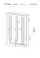
- FIG. 1illustrates an antenna system 100 constructed according to the present invention.
- the antenna system 100includes a first antenna element 104 , a second antenna element 106 and a third antenna element 108 disposed upon a dielectric layer 110 that resides upon a radio module shell 102 .
- a first phase shifting element 112connects the first antenna element 104 to a common antenna connection 118 while second 114 and third 116 phase shifting elements connect the second 106 and third 108 antenna elements to the common antenna connection 118 , respectively.
- antenna elementsAs is known, operating characteristics of antenna elements vary with the size, shape, resitivity, proximity to dielectric and conductive structures as well as with various other physical properties of the antenna elements. Each of the antenna elements in the embodiment illustrated in FIG. 1 has similar operating characteristics due to their similar construction. However, in other embodiments, to be described later herein, operating characteristics of the antenna elements vary.
- the particular antenna system 100 system illustrated in FIG. 1is designed to operate over a frequency range reserved for spread-spectrum communications, the range generally extending from 902 to 928 Megahertz (MHz).
- MHzMegahertz
- an operating difficulty associated with many wireless devicesrelates to the protruding nature of conventional antennas. While protruding antennas may present few problems when used with stationary wireless devices not limited to a physical space, protruding antennas often interfere with the operation of portable units, such as hand-held terminals, the antennas often being damaged during use. Therefore, as illustrated in FIG. 1, the antenna system 100 according to the present invention does not protrude from the radio module shell 102 upon which it is mounted so that it may not be damaged during normal use. Further, when attached to a host unit, such as a portable terminal, the antenna system 100 does not protrude from the portable terminal in a fashion which interferes with the operation of the portable terminal.
- the antenna system 100In the design of the antenna system 100 of FIG. 1, performance across a frequency design range, e.g. 902 MHz to 928 MHz, is required.
- the use of relatively small antenna elements 104 , 106 and 108 such as those illustrated in FIG. 1typically produces a narrow bandwidth due to the small dimensions of the antenna elements relative to wavelengths in the frequency design range.
- each of the antenna elements 104 , 106 and 108exhibits adequate performance across a relatively narrow bandwidth.
- the antenna system 100employs the phase shifting elements 112 , 114 and 116 to frequency shift the bandwidths of each of the antenna elements 104 , 106 and 108 .
- the bandwidthsare presented at the common antenna connection 118 .
- the antenna system 100exhibits a wider bandwidth than does any of the antenna elements 104 , 106 and 108 individually.
- Phase shifting elements 112 , 114 and 116provide transmission paths of varying lengths between their respective antenna elements and the common antenna connection 118 , the respective phase shifts also providing the desired bandwidth shifts.
- FIG. 2Ais an schematic diagram illustrating generally an equivalent circuit of an antenna system 200 similar to the antenna system 100 of FIG. 1 .
- FIG. 2Ashows four antenna elements 202 , 204 , 206 and 208 .
- the antenna elements 202 , 204 , 206 and 208connect to a common antenna connection 218 via phase shifting elements 210 , 212 , 214 and 216 , respectively.
- the circuitry connection 220phase shifts the impedance of the antenna system at the common antenna connection 218 prior to its connection to radio circuitry 222 .
- the circuitry connection 220is designed so that the impedance presented to the radio circuitry is minimized at harmonics of the frequency design range while providing satisfactory performance over the frequency design range.
- the circuitry connection 220transforms the impedance of the antenna system at the common antenna connection 218 so that it presents a short to the radio circuitry 222 . Impedance transformations, as well as bandwidth shifting, using same or similar techniques, is known in the art and will not be further described herein except to expand upon the teachings of the present invention.
- FIG. 2Bis a schematic diagram similar to FIG. 2A but in addition showing an exemplary embodiment of a circuitry connector 220 according to the present invention. Numbering conventions remain consistent with FIG. 2A for common elements.
- the impedance at the common antenna connection 218may be transformed using a section of transmission line, the length of which in wavelengths at a harmonic of the frequency design range, transforms the impedance so as to present a short circuit (or minimum impedance) to the radio circuitry 222 at the harmonic of the frequency design range.
- the radio circuitry 222can deliver no power for transmission to the antenna elements 202 , 204 , 206 and 208 , thus complying with FCC requirements.
- the circuitry connector 220may include tuning stubs, shorts or lumped elements to assist in presenting a short circuit (or minimum impedance) to the radio circuitry 222 at the harmonic frequencies of the frequency design range.
- FIG. 3is a collection of graphs illustrating operating characteristics of an antenna system according to the present invention as compared to individual antenna characteristics.
- the collection of graphscompares characteristics of a three antenna element antenna system, same or similar to the antenna system 100 of FIG. 1, to characteristics of individual antennas.
- Each of the graphsplots return loss in decibels (dB) on the vertical axis versus frequency on the horizontal axis. Return loss is a measure of energy not radiated by an antenna which “returns” to the radio circuitry.
- dBdecibels
- UHF antenna return loss characteristics 302shows that a respective UHF antenna has a minimum return loss at a center design frequency 303 at which point the antenna provides maximum transmission of energy delivered to it by the radio circuitry. While the UHF antenna exhibits a relatively wide bandwidth, its relatively large construction is unsuitable for those uses contemplated by the antenna system according to the present invention.
- One-element antenna return loss characteristics 304provide a minimum return loss at a center design frequency 305 but has a relatively narrow bandwidth. Such return loss characteristics may be produced by one of the antenna elements 104 , 106 or 108 of the antenna system 100 illustrated in FIG. 1 .
- the return loss characteristics 306 of a three-element antenna system wherein the bandwidths of the antenna elements are frequency shifted with respect to one anotherproduces minimum return loss at three separate frequencies 307 , 308 and 309 . With the frequency shifting of these three elements correctly executed, bandwidths of the antenna elements overlap to produce the three-element antenna system return loss characteristics 310 illustrated, such return loss characteristics corresponding to the antenna system 100 illustrated with reference to FIG. 1 . As is illustrated, the bandwidth 312 extends across the frequency design range, 902 to 928 MHz in the present embodiment.
- the teachings of the present inventionmay be extended to antenna systems having two antenna elements or in excess of three antenna elements, depending upon the requirements of the particular design. As is apparent from FIG. 3, application of the teachings of present invention for a five antenna element system, for example, would produce return loss characteristics across a design range with five sub-minimas of return loss, each of the sub-minimas corresponding to one of the five antenna elements of the antenna system.
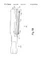
- FIG. 4Ais a sectional side view of a radio module 400 including an antenna system according to the present invention.
- the radio module 400includes a radio module shell 402 formed of a thin, light-weight metal and adapted to be received by a portable terminal, such as a hand-held portable data terminal.
- the radio module 400interfaces with a host system via a PCMCIA, PCI, ISA or other standard or proprietary interface.
- the radio module 400could also be received by other portable devices such as code readers, scanners, printers and other portable devices that employ wireless communications. Further, the radio module 400 could also be used with a stationary device as well.
- the radio moduleincludes radio circuitry 404 contained within the radio module shell 402 .
- the radio circuitry 404includes, for example, a radio processor, a radio transceiver, memory, host interface circuitry and various other circuitry mounted on a printed circuit board 405 held in place within the radio module shell 402 by insulating mounts 406 .
- the circuitry connector 408is partially mounted upon the circuit board 405 that also contains the radio circuitry 404 . However, in other embodiments, the circuitry connector 408 may be disposed on an inner surface of the radio module shell 402 . When the circuitry connector 408 is disposed upon an inner surface of the radio module shell 402 , the circuitry connector 408 must be electrically isolated from the conductive radio module shell 402 . As an example of the construction that may be employed, the circuitry connector 408 may include an insulated cable 409 that extends through the radio module shell 402 to make connection at the common antenna connection.
- An antenna element 410(other antenna elements are not shown since the FIG. is a side view) resides upon a dielectric layer 412 , both of which conform to an outer surface of the radio module shell 402 .
- the dielectric layer 412comprises a dielectric having a relatively small dielectric constant. Teflon, for example, has a relative dielectric constant of approximately 2.2 and enhances operation of the antenna element 410 by effectively reducing the wavelength of radiated waves.
- shorter antenna elements 410may employed to produce equivalent performance when using the relatively lower dielectric constant material for the dielectric layer 412 .
- FIG. 4Bis a sectional side view of an alternative radio module 450 including an antenna system according to the present invention.
- the radio module 450differs from the radio module 400 of FIG. 4A in that an antenna element 460 (one of a plurality) is raised above a dielectric layer 452 that provides insulation from the conductive radio module shell 402 .
- Insulative spacers 454formed of nylon, for example, support the antenna element 460 above the dielectric layer 452 at an angle with respect to the dielectric layer 452 .
- FIG. 4Cis a diagrammatic perspective view of a radio module 470 having an antenna system constructed according to the present invention, similar to the antenna system illustrated with reference to FIG. 4 B.
- the antenna systemincludes first 472 , second 474 and third 476 antenna elements raised above a dielectric layer 478 residing upon the radio module shell 402 .
- Insulating spacers 480connect the antenna elements 472 , 474 and 476 to the dielectric layer 478 , positioning the elements so that an array formed by the elements has improved performance.
- a first end 482 of first antenna element 472resides more closely to the dielectric layer 478 than does a second end 484 of the first antenna element 472 .
- a longitudinal axis of the first antenna element 472resides non-parallel to the dielectric layer 478 .
- a horizontal axis of the first antenna element 472also resides non-parallel to the dielectric layer.
- the second antenna element 472resides substantially parallel to the surface of the dielectric layer 478 .
- the third antenna element 474orients to complement orientation of the first antenna element 470 so that, in combination, the antenna elements provide enhanced performance over a desired frequency range.
- FIG. 5Ais a sectional side view of a portable terminal 500 A having a radio module 502 that includes an antenna system according to the present invention.
- the portable terminal 500 Amay include, for example, terminal processing circuitry, a display, a keypad, a battery pack and other components that may be required to perform data collection, data processing and data communication functions. While installation of the radio module 502 within the portable terminal 500 A is illustrated, the radio module 502 could also be installed within scanners, code readers, digital cameras, portable printers, data pads and other units requiring a wireless communication link with a remote location.
- a thin, lightweight metal radio module shell 503houses radio circuitry 504 as well as a circuitry connector 512 that performs the previously described impedance transformations.
- the radio circuitry 504includes interface circuitry that allows the radio module 502 to communicate with the portable terminal 500 A.
- a first antenna element 508resides atop a dielectric layer 506 that isolates the first antenna element 508 from the radio module shell 503 . Additional antenna elements are not shown in this sectional side view but reside adjacent the first antenna element 508 , the construction similar to that illustrated with reference to FIG. 1 .
- the circuitry connector 512includes a short insulated cable section 514 that passes through a hole formed in the radio module shell 503 and that makes connection with the first antenna element 508 via a common antenna connection.
- the antenna elements of the illustrated radio module 502reside directly upon the dielectric layer 506 which resides directly upon the radio module shell 503 .
- the configurationrequires a dielectric with a relatively low dielectric constant for maximum performance.
- a protective covering 510 that is transmissive to generated radio wavesmay be constructed simply and inexpensively to protect the antenna elements and those portions of the dielectric layer exposed.
- FIG. 5Bis a sectional side view of a portable terminal 500 B having a radio module 520 that includes an alternative embodiment of an antenna system according to the present invention.
- the first antenna element 522 of the radio module 520is supported adjacent the dielectric layer 506 by insulating spacers 524 , such construction similar to that illustrated with respect to FIG. 4 C.
- protective cover 526constructed of a material transmissive at radio frequencies extends beyond the antenna elements and provides a barrier to contact.
- FIG. 5Cis a sectional side view of a portable terminal 500 C having a radio module 550 that incorporates another embodiment of an antenna system according to the present invention.
- the radio module 550houses radio circuitry as well as the components of the antenna system.
- the radio module shell 553is transmissive to radio waves produced by the antenna system and is constructed of plastic or another transmissive material that provides protection to the components housed within the radio module shell 553 .
- Radio circuitry componentsare disposed upon a printed circuit board 554 mounted within the radio module shell 553 .
- the printed circuit board 556includes shielding that shields the radio circuitry components from transmissions produced by the antenna elements.
- a dielectric layer 556connects directly to the shielded printed circuit board with the antenna elements residing atop the dielectric layer 556 .
- the first antenna element 552as well as additional antenna elements, not shown, couple to the radio circuitry via a circuitry connector 512 that includes a shielded cable 514 that that extends through the printed circuit board 556 and
- FIG. 5Dis a sectional side view of a portable terminal 500 D having a radio module 570 that includes still another alternative embodiment of an antenna system according to the present invention.
- Construction of the radio module 570is similar to that of the radio module 550 illustrated with respect to FIG. SC except that the first antenna element 572 (as well as other antenna elements) are located apart from the dielectric layer 556 , mounted via insulative spacers 574 .
- a dielectric having a different dielectric constantmay be used with the construction of FIG. 5D to obtain performance similar to that obtained by the construction of FIG. 5 C.
- FIG. 6Ais a diagrammatic top view of a portion of an antenna system 600 according to the present invention.
- antenna elements 600are disposed upon a dielectric layer 602 and are formed of a conductive material such as a thin layer of copper.
- First 608 , second 610 and third 612 antenna elementsare cut separately from a sheet of copper using techniques known in the art and then be disposed upon the dielectric layer 602 .
- the antenna elementsmay be either disposed directly upon the dielectric layer or be attached by insulative spacers 620 so that at least some of the antenna elements reside above the dielectric layer 602 .
- First 614 and second 616 phase shifting elementscouple antenna elements 608 , 610 and 612 , respectively, to a common antenna connection 618 .
- a circuitry connector(not shown) connects the common antenna connection 618 to radio circuitry (not shown) in a manner previously described.
- the phase shifting elements 614 and 616provide transmission paths of varying length between the common antenna connection 618 and respective antenna elements. In this fashion, the bandwidth of respective antenna elements is shifted prior to connection at the common antenna connection 618 to produce the relatively wide bandwidth of the antenna system as a whole.
- the phase shifting elements 614 and 616may also have characteristic impedances that are tailored so as to perform the designed phase shifting.
- Impedance matching elements 603 , 604 , 615 , 617 , 619 and 621are designed such that the impedances of the antenna elements 608 , 610 and 612 at connection points to the phase shifting elements 614 and 616 match the impedance of the phase shifting elements 614 and 616 .
- the length and width of these impedance matching elementsare designed to perform such impedance matching.
- the impedance of each phase shifting element 614 and 616is approximately 150 Ohms.
- the impedance matching elements 603 , 604 , 615 , 617 , 619 and 621are designed, therefore, to match such 50 Ohm impedance at corresponding connection points.
- the combined impedance at the antenna connector 618is then the parallel combination of three 150 Ohm loads, which is 50 Ohms.
- 50 Ohmsis the impedance seen by connected radio circuitry, such impedance at the desired design input level.
- FIG. 6Bis a diagrammatic top view of an alternative embodiment of an antenna system 640 according to the present invention.
- a first 642 and second 644 antenna elementsare disposed upon or substantially adjacent to a dielectric layer 602 .
- Insulative spacers 620may be employed to physically separate all or a portion of the antenna elements 642 and 644 from the dielectric layer 602 to enhance performance of the antenna system 640 .
- a phase shifting element 648couples the second antenna element 644 to a common antenna connection 650 with a phase shift.
- the design of such phase shifting element 648shifts the bandwidth of antenna element 644 so that the bandwidth of the antenna element in combination with the bandwidth of antenna element 642 exceeds the individual bandwidths of the antenna elements 642 and 644 .
- Impedance matching elements 649 and 651match the impedance of antenna element 644 to phase shifting element 648 .
- impedance matching elements 646 and 647match the impedance of antenna element 642 to the phase shifting element 648 and such that a design impedance is presented at the common antenna connection 650 .
- the antenna system 640provides a relatively wider bandwidth from a relatively smaller antenna package.
- the principles discussed with respect to construction of an antenna system according to the present inventionmay be extended to a greater number of antenna elements using the same or similar principles.
- FIG. 6Cis a diagrammatic top view of still another embodiment of an antenna system 670 according to the present invention.
- the antenna system 670includes a first antenna element 672 that conforms to radio circuitry contained within a radio module or to an inner surface of a radio module shell in which it is contained.
- the antenna system 670may be contained in a radio module, such as the one illustrated with respect to FIG. 5 C.
- the antenna elementsmay be disposed outside of the radio module shell in a pattern to enhance gain or bandwidth of each antenna element or the antenna system as a whole.
- a second antenna element 674may include a standard shape such as that illustrated, or may include an differing shape designed to conform to other components within the radio module.
- Phase shifting element 676couples the antenna element 674 to a common antenna connection 618 .
- Impedance matching elements 681 and 683match the impedance of the antenna element 674 to the phase shifting element.
- impedance matching elements 678 and 679match the impedance of antenna element 672 to the impedance of the phase shifting element 676 and such that a design impedance is presented at the common antenna connection 618 .
- a circuitry connectorsuch as one previously described, couples the common antenna connection 618 to radio circuitry contained within the radio module.
Landscapes
- Engineering & Computer Science (AREA)
- Computer Networks & Wireless Communication (AREA)
- Physics & Mathematics (AREA)
- Electromagnetism (AREA)
- Support Of Aerials (AREA)
- Details Of Aerials (AREA)
Abstract
Description
Claims (16)
Priority Applications (1)
| Application Number | Priority Date | Filing Date | Title |
|---|---|---|---|
| US08/888,660US6281850B1 (en) | 1996-02-16 | 1997-07-07 | Broadband multiple element antenna system |
Applications Claiming Priority (3)
| Application Number | Priority Date | Filing Date | Title |
|---|---|---|---|
| US1184496P | 1996-02-16 | 1996-02-16 | |
| US80039997A | 1997-02-14 | 1997-02-14 | |
| US08/888,660US6281850B1 (en) | 1996-02-16 | 1997-07-07 | Broadband multiple element antenna system |
Related Parent Applications (1)
| Application Number | Title | Priority Date | Filing Date |
|---|---|---|---|
| US80039997AContinuation-In-Part | 1996-02-16 | 1997-02-14 |
Publications (1)
| Publication Number | Publication Date |
|---|---|
| US6281850B1true US6281850B1 (en) | 2001-08-28 |
Family
ID=26682860
Family Applications (1)
| Application Number | Title | Priority Date | Filing Date |
|---|---|---|---|
| US08/888,660Expired - LifetimeUS6281850B1 (en) | 1996-02-16 | 1997-07-07 | Broadband multiple element antenna system |
Country Status (1)
| Country | Link |
|---|---|
| US (1) | US6281850B1 (en) |
Cited By (26)
| Publication number | Priority date | Publication date | Assignee | Title |
|---|---|---|---|---|
| US20020000937A1 (en)* | 2000-03-23 | 2002-01-03 | Osamu Kozakai | Antenna apparatus and a portable wireless communication apparatus using the same |
| US20030030586A1 (en)* | 2001-08-13 | 2003-02-13 | International Business Machines Corporation | Flexible printed antenna and apparatus utilizing the same |
| US6535172B2 (en)* | 2000-09-19 | 2003-03-18 | Sony Corporation | Antenna device and radio communication card module having antenna device |
| US20030184482A1 (en)* | 2002-03-04 | 2003-10-02 | Ulrich Bettin | Multi-band PIF antenna with meander structure |
| WO2003075395A3 (en)* | 2002-03-04 | 2004-03-18 | Siemens Inf & Comm Mobile Llc | Multi-band pif antenna with meander structure |
| JP2004112397A (en)* | 2002-09-19 | 2004-04-08 | Yokohama Tlo Co Ltd | Multi-frequency shared antenna and multi-band transmitter-receiver |
| US20040145533A1 (en)* | 2003-01-24 | 2004-07-29 | Taubman Irving Louis | Combined mechanical package shield antenna |
| US20050092845A1 (en)* | 2003-11-03 | 2005-05-05 | Forster Ian J. | Self-compensating antennas for substrates having differing dielectric constant values |
| US20060055542A1 (en)* | 2004-09-13 | 2006-03-16 | Forster Ian J | RFID device with content insensitivity and position insensitivity |
| US20060054710A1 (en)* | 2003-04-10 | 2006-03-16 | Forster Ian J | RFID devices having self-compensating antennas and conductive shields |
| US20060091225A1 (en)* | 2003-11-04 | 2006-05-04 | Forster Ian J | RFID tag using a surface insensitive antenna structure |
| US20060192714A1 (en)* | 2005-02-25 | 2006-08-31 | Kyocera Corporation | Wireless communication terminal device |
| US20060208956A1 (en)* | 2003-11-24 | 2006-09-21 | Emanoil Surducan | Modified printed dipole antennas for wireless multi-band communication systems |
| US20070141760A1 (en)* | 2005-12-21 | 2007-06-21 | Ferguson Scott W | Electrical device and method of manufacturing electrical devices using film embossing techniques to embed integrated circuits into film |
| US20070216584A1 (en)* | 2004-05-31 | 2007-09-20 | Tomoaki Nishikido | Portable Wireless Device |
| US20080106478A1 (en)* | 2006-11-06 | 2008-05-08 | Hill Robert J | Broadband antenna with coupled feed for handheld electronic devices |
| US20090273531A1 (en)* | 2007-01-19 | 2009-11-05 | Murata Manufacturing Co.,Ltd. | Antenna device and wireless communication apparatus |
| US20090318094A1 (en)* | 2006-06-08 | 2009-12-24 | Fractus, S.A. | Distributed antenna system robust to human body loading effects |
| US20090315718A1 (en)* | 2008-06-19 | 2009-12-24 | Omron Corporation | RFID inlay structure and method of manufacturing RFID inlay structure |
| US20100259454A1 (en)* | 2006-06-30 | 2010-10-14 | Jussi Rahola | Mechanically tunable antenna for communication devices |
| US20110175705A1 (en)* | 2010-01-19 | 2011-07-21 | Symbol Technologies, Inc. | Passive rfid triggering systems and methods using antenna reverse power detection |
| US8368602B2 (en) | 2010-06-03 | 2013-02-05 | Apple Inc. | Parallel-fed equal current density dipole antenna |
| US20130162483A1 (en)* | 2011-12-27 | 2013-06-27 | Kyungsoon Park | Antenna assembly, method of manufacturing antenna assembly and mobile terminal having antenna assembly |
| US10062973B2 (en) | 2013-06-20 | 2018-08-28 | Fractus Antennas, S.L. | Scattered virtual antenna technology for wireless devices |
| JP2018157315A (en)* | 2017-03-16 | 2018-10-04 | カシオ計算機株式会社 | ANTENNA DEVICE AND ELECTRONIC DEVICE |
| CN112448130A (en)* | 2019-09-05 | 2021-03-05 | 北京小米移动软件有限公司 | Electronic device |
Citations (2)
| Publication number | Priority date | Publication date | Assignee | Title |
|---|---|---|---|---|
| US4356492A (en)* | 1981-01-26 | 1982-10-26 | The United States Of America As Represented By The Secretary Of The Navy | Multi-band single-feed microstrip antenna system |
| US5440318A (en)* | 1990-08-22 | 1995-08-08 | Butland; Roger J. | Panel antenna having groups of dipoles fed with insertable delay lines for electrical beam tilting and a mechanically tiltable ground plane |
- 1997
- 1997-07-07USUS08/888,660patent/US6281850B1/ennot_activeExpired - Lifetime
Patent Citations (2)
| Publication number | Priority date | Publication date | Assignee | Title |
|---|---|---|---|---|
| US4356492A (en)* | 1981-01-26 | 1982-10-26 | The United States Of America As Represented By The Secretary Of The Navy | Multi-band single-feed microstrip antenna system |
| US5440318A (en)* | 1990-08-22 | 1995-08-08 | Butland; Roger J. | Panel antenna having groups of dipoles fed with insertable delay lines for electrical beam tilting and a mechanically tiltable ground plane |
Cited By (52)
| Publication number | Priority date | Publication date | Assignee | Title |
|---|---|---|---|---|
| US20020000937A1 (en)* | 2000-03-23 | 2002-01-03 | Osamu Kozakai | Antenna apparatus and a portable wireless communication apparatus using the same |
| EP1137100A3 (en)* | 2000-03-23 | 2003-12-17 | Sony Corporation | Antenna apparatus and a portable wireless communication apparatus using the same |
| US6894648B2 (en) | 2000-03-23 | 2005-05-17 | Sony Corporation | Antenna apparatus and a portable wireless communication apparatus using the same |
| US6535172B2 (en)* | 2000-09-19 | 2003-03-18 | Sony Corporation | Antenna device and radio communication card module having antenna device |
| US6778139B2 (en)* | 2001-08-13 | 2004-08-17 | International Business Machines Corporation | Flexible printed antenna and apparatus utilizing the same |
| US20030030586A1 (en)* | 2001-08-13 | 2003-02-13 | International Business Machines Corporation | Flexible printed antenna and apparatus utilizing the same |
| US6856285B2 (en) | 2002-03-04 | 2005-02-15 | Siemens Information & Communication Mobile, Llc | Multi-band PIF antenna with meander structure |
| CN1650473B (en)* | 2002-03-04 | 2012-05-30 | 西门子信息及移动通讯有限公司 | Broadband planar inverted f antenna with curved structure |
| US6882318B2 (en) | 2002-03-04 | 2005-04-19 | Siemens Information & Communications Mobile, Llc | Broadband planar inverted F antenna |
| US20030184482A1 (en)* | 2002-03-04 | 2003-10-02 | Ulrich Bettin | Multi-band PIF antenna with meander structure |
| WO2003075395A3 (en)* | 2002-03-04 | 2004-03-18 | Siemens Inf & Comm Mobile Llc | Multi-band pif antenna with meander structure |
| JP2004112397A (en)* | 2002-09-19 | 2004-04-08 | Yokohama Tlo Co Ltd | Multi-frequency shared antenna and multi-band transmitter-receiver |
| US6842149B2 (en) | 2003-01-24 | 2005-01-11 | Solectron Corporation | Combined mechanical package shield antenna |
| US20040145533A1 (en)* | 2003-01-24 | 2004-07-29 | Taubman Irving Louis | Combined mechanical package shield antenna |
| US20070080233A1 (en)* | 2003-04-10 | 2007-04-12 | Forster Ian J | RFID tag using a surface insensitive antenna structure |
| US20060054710A1 (en)* | 2003-04-10 | 2006-03-16 | Forster Ian J | RFID devices having self-compensating antennas and conductive shields |
| US7652636B2 (en) | 2003-04-10 | 2010-01-26 | Avery Dennison Corporation | RFID devices having self-compensating antennas and conductive shields |
| US7379024B2 (en) | 2003-04-10 | 2008-05-27 | Avery Dennison Corporation | RFID tag using a surface insensitive antenna structure |
| US7055754B2 (en)* | 2003-11-03 | 2006-06-06 | Avery Dennison Corporation | Self-compensating antennas for substrates having differing dielectric constant values |
| US20050092845A1 (en)* | 2003-11-03 | 2005-05-05 | Forster Ian J. | Self-compensating antennas for substrates having differing dielectric constant values |
| US7501984B2 (en) | 2003-11-04 | 2009-03-10 | Avery Dennison Corporation | RFID tag using a surface insensitive antenna structure |
| US20060091225A1 (en)* | 2003-11-04 | 2006-05-04 | Forster Ian J | RFID tag using a surface insensitive antenna structure |
| US20060208956A1 (en)* | 2003-11-24 | 2006-09-21 | Emanoil Surducan | Modified printed dipole antennas for wireless multi-band communication systems |
| US20070216584A1 (en)* | 2004-05-31 | 2007-09-20 | Tomoaki Nishikido | Portable Wireless Device |
| US7453405B2 (en)* | 2004-05-31 | 2008-11-18 | Panasonic Corporation | Portable wireless device |
| US7501955B2 (en) | 2004-09-13 | 2009-03-10 | Avery Dennison Corporation | RFID device with content insensitivity and position insensitivity |
| US20060055542A1 (en)* | 2004-09-13 | 2006-03-16 | Forster Ian J | RFID device with content insensitivity and position insensitivity |
| US7280075B2 (en)* | 2005-02-25 | 2007-10-09 | Kyocera Corporation | Wireless communication terminal device |
| US20060192714A1 (en)* | 2005-02-25 | 2006-08-31 | Kyocera Corporation | Wireless communication terminal device |
| US20070141760A1 (en)* | 2005-12-21 | 2007-06-21 | Ferguson Scott W | Electrical device and method of manufacturing electrical devices using film embossing techniques to embed integrated circuits into film |
| US8067253B2 (en) | 2005-12-21 | 2011-11-29 | Avery Dennison Corporation | Electrical device and method of manufacturing electrical devices using film embossing techniques to embed integrated circuits into film |
| US10411364B2 (en) | 2006-06-08 | 2019-09-10 | Fractus Antennas, S.L. | Distributed antenna system robust to human body loading effects |
| US9007275B2 (en)* | 2006-06-08 | 2015-04-14 | Fractus, S.A. | Distributed antenna system robust to human body loading effects |
| US20090318094A1 (en)* | 2006-06-08 | 2009-12-24 | Fractus, S.A. | Distributed antenna system robust to human body loading effects |
| US10033114B2 (en) | 2006-06-08 | 2018-07-24 | Fractus Antennas, S.L. | Distributed antenna system robust to human body loading effects |
| US20100259454A1 (en)* | 2006-06-30 | 2010-10-14 | Jussi Rahola | Mechanically tunable antenna for communication devices |
| US8212729B2 (en)* | 2006-06-30 | 2012-07-03 | Nokia Corporation | Mechanically tunable antenna for communication devices |
| US20080106478A1 (en)* | 2006-11-06 | 2008-05-08 | Hill Robert J | Broadband antenna with coupled feed for handheld electronic devices |
| US7688267B2 (en) | 2006-11-06 | 2010-03-30 | Apple Inc. | Broadband antenna with coupled feed for handheld electronic devices |
| US20090273531A1 (en)* | 2007-01-19 | 2009-11-05 | Murata Manufacturing Co.,Ltd. | Antenna device and wireless communication apparatus |
| JPWO2008087780A1 (en)* | 2007-01-19 | 2010-05-06 | 株式会社村田製作所 | ANTENNA DEVICE AND RADIO COMMUNICATION DEVICE |
| US8279121B2 (en) | 2007-01-19 | 2012-10-02 | Murata Manufacturing Co., Ltd. | Antenna device and wireless communication apparatus |
| US20090315718A1 (en)* | 2008-06-19 | 2009-12-24 | Omron Corporation | RFID inlay structure and method of manufacturing RFID inlay structure |
| US7999677B2 (en)* | 2008-06-19 | 2011-08-16 | Omron Corporation | RFID inlay structure and method of manufacturing RFID inlay structure |
| US20110175705A1 (en)* | 2010-01-19 | 2011-07-21 | Symbol Technologies, Inc. | Passive rfid triggering systems and methods using antenna reverse power detection |
| US9087247B2 (en)* | 2010-01-19 | 2015-07-21 | Symbol Technologies, Llc | Passive RFID triggering systems and methods using antenna reverse power detection |
| US8368602B2 (en) | 2010-06-03 | 2013-02-05 | Apple Inc. | Parallel-fed equal current density dipole antenna |
| US20130162483A1 (en)* | 2011-12-27 | 2013-06-27 | Kyungsoon Park | Antenna assembly, method of manufacturing antenna assembly and mobile terminal having antenna assembly |
| US10062973B2 (en) | 2013-06-20 | 2018-08-28 | Fractus Antennas, S.L. | Scattered virtual antenna technology for wireless devices |
| JP2018157315A (en)* | 2017-03-16 | 2018-10-04 | カシオ計算機株式会社 | ANTENNA DEVICE AND ELECTRONIC DEVICE |
| CN112448130A (en)* | 2019-09-05 | 2021-03-05 | 北京小米移动软件有限公司 | Electronic device |
| US11031701B2 (en)* | 2019-09-05 | 2021-06-08 | Beijing Xiaomi Mobile Software Co., Ltd. | Electronic device |
Similar Documents
| Publication | Publication Date | Title |
|---|---|---|
| US6281850B1 (en) | Broadband multiple element antenna system | |
| US6195049B1 (en) | Micro-strip patch antenna for transceiver | |
| US6424300B1 (en) | Notch antennas and wireless communicators incorporating same | |
| EP0847103B1 (en) | Shared antenna and portable radio device using the same | |
| JP3004533B2 (en) | Antenna device | |
| US6593897B1 (en) | Wireless GPS apparatus with integral antenna device | |
| US6326919B1 (en) | Patch antenna | |
| US20040090378A1 (en) | Multi-band antenna structure | |
| EP1328069B1 (en) | EMC-arrangement for a device employing wireless data transfer | |
| US6339405B1 (en) | Dual band dipole antenna structure | |
| US20010015705A1 (en) | Slot antenna device | |
| AU714256B2 (en) | Method and apparatus for coupling signals | |
| AU5457298A (en) | Dual-band antenna coupler for a portable radiotelephone | |
| US6052090A (en) | Multi-band antenna | |
| KR20010075231A (en) | Capacitively-tune broadband antenna structure | |
| US6947011B2 (en) | Connector unit | |
| US6882319B2 (en) | Antenna module whose antenna characteristics are not adversely affected by a mother board | |
| KR100589296B1 (en) | Wireless device with a movable antenna | |
| KR20010052132A (en) | Retractable radiotelephone antennas with extended feeds | |
| US20020123312A1 (en) | Antenna systems including internal planar inverted-F Antenna coupled with external radiating element and wireless communicators incorporating same | |
| US20080272964A1 (en) | Antenna Radiator Assembly and Radio Communications Assembly | |
| US6052089A (en) | Half-wave retractable antenna with matching helix | |
| WO1994026000A1 (en) | Anti-electromagnetic field antenna for cellular telephone | |
| US6041220A (en) | Portable radio communication apparatus | |
| JP4372325B2 (en) | antenna |
Legal Events
| Date | Code | Title | Description |
|---|---|---|---|
| AS | Assignment | Owner name:NORAND CORPORATION, IOWA Free format text:ASSIGNMENT OF ASSIGNORS INTEREST;ASSIGNOR:KLOSTERMANN, DANIEL J.;REEL/FRAME:009098/0869 Effective date:19970806 | |
| AS | Assignment | Owner name:INTERMEC IP CORP., CALIFORNIA Free format text:ASSIGNMENT OF ASSIGNORS INTEREST;ASSIGNOR:INTERMEC TECHNOLOGIES CORPORATION;REEL/FRAME:011746/0403 Effective date:19990721 Owner name:INTERMEC TECHNOLOGIES CORPORATION, WASHINGTON Free format text:MERGER;ASSIGNOR:NORAND CORPORATION;REEL/FRAME:011746/0481 Effective date:19971228 Owner name:INTERMEC IP CORP., CALIFORNIA Free format text:CHANGE OF NAME;ASSIGNOR:NORAND TECHNOLOGY CORPORATION;REEL/FRAME:011746/0503 Effective date:19980318 | |
| AS | Assignment | Owner name:INTERMEC IP CORP., CALIFORNIA Free format text:ASSIGNMENT OF ASSIGNORS INTEREST;ASSIGNOR:INTERMEC TECHNOLOGIES CORPORATION;REEL/FRAME:012065/0300 Effective date:19990721 | |
| STCF | Information on status: patent grant | Free format text:PATENTED CASE | |
| AS | Assignment | Owner name:BROADCOM CORPORATION, CALIFORNIA Free format text:ASSIGNMENT OF ASSIGNORS INTEREST;ASSIGNOR:INTERMEC IP CORP.;REEL/FRAME:013712/0241 Effective date:20021224 | |
| FPAY | Fee payment | Year of fee payment:4 | |
| FPAY | Fee payment | Year of fee payment:8 | |
| FPAY | Fee payment | Year of fee payment:12 | |
| SULP | Surcharge for late payment | Year of fee payment:11 | |
| REMI | Maintenance fee reminder mailed | ||
| AS | Assignment | Owner name:BANK OF AMERICA, N.A., AS COLLATERAL AGENT, NORTH CAROLINA Free format text:PATENT SECURITY AGREEMENT;ASSIGNOR:BROADCOM CORPORATION;REEL/FRAME:037806/0001 Effective date:20160201 Owner name:BANK OF AMERICA, N.A., AS COLLATERAL AGENT, NORTH Free format text:PATENT SECURITY AGREEMENT;ASSIGNOR:BROADCOM CORPORATION;REEL/FRAME:037806/0001 Effective date:20160201 | |
| AS | Assignment | Owner name:AVAGO TECHNOLOGIES GENERAL IP (SINGAPORE) PTE. LTD., SINGAPORE Free format text:ASSIGNMENT OF ASSIGNORS INTEREST;ASSIGNOR:BROADCOM CORPORATION;REEL/FRAME:041706/0001 Effective date:20170120 Owner name:AVAGO TECHNOLOGIES GENERAL IP (SINGAPORE) PTE. LTD Free format text:ASSIGNMENT OF ASSIGNORS INTEREST;ASSIGNOR:BROADCOM CORPORATION;REEL/FRAME:041706/0001 Effective date:20170120 | |
| AS | Assignment | Owner name:BROADCOM CORPORATION, CALIFORNIA Free format text:TERMINATION AND RELEASE OF SECURITY INTEREST IN PATENTS;ASSIGNOR:BANK OF AMERICA, N.A., AS COLLATERAL AGENT;REEL/FRAME:041712/0001 Effective date:20170119 | |
| AS | Assignment | Owner name:AVAGO TECHNOLOGIES INTERNATIONAL SALES PTE. LIMITE Free format text:ASSIGNMENT OF ASSIGNORS INTEREST;ASSIGNOR:AVAGO TECHNOLOGIES GENERAL IP (SINGAPORE) PTE. LTD.;REEL/FRAME:047022/0620 Effective date:20180509 | |
| AS | Assignment | Owner name:AVAGO TECHNOLOGIES INTERNATIONAL SALES PTE. LIMITE Free format text:CORRECTIVE ASSIGNMENT TO CORRECT THE NATURE OF CONVEYANCE AND EFFECTIVE DATE PREVIOUSLY RECORDED ON REEL 047022 FRAME 0620. ASSIGNOR(S) HEREBY CONFIRMS THE MERGER;ASSIGNOR:AVAGO TECHNOLOGIES GENERAL IP (SINGAPORE) PTE. LTD.;REEL/FRAME:047185/0643 Effective date:20180509 | |
| AS | Assignment | Owner name:AVAGO TECHNOLOGIES INTERNATIONAL SALES PTE. LIMITE Free format text:CORRECTIVE ASSIGNMENT TO CORRECT THE EFFECTIVE DATE PREVIOUSLY RECORDED ON REEL 047185 FRAME 0643. ASSIGNOR(S) HEREBY CONFIRMS THE MERGER;ASSIGNOR:AVAGO TECHNOLOGIES GENERAL IP (SINGAPORE) PTE. LTD.;REEL/FRAME:047476/0845 Effective date:20180905 | |
| AS | Assignment | Owner name:AVAGO TECHNOLOGIES INTERNATIONAL SALES PTE. LIMITE Free format text:CORRECTIVE ASSIGNMENT TO CORRECT THE EFFECTIVE DATE OF MERGER PREVIOUSLY RECORDED AT REEL: 047185 FRAME: 0643. ASSIGNOR(S) HEREBY CONFIRMS THE CORRECTIVE MERGER;ASSIGNOR:AVAGO TECHNOLOGIES GENERAL IP (SINGAPORE) PTE. LTD.;REEL/FRAME:047959/0296 Effective date:20180905 |