US6281838B1 - Base-3 switched-line phase shifter using micro electro mechanical (MEMS) technology - Google Patents
Base-3 switched-line phase shifter using micro electro mechanical (MEMS) technologyDownload PDFInfo
- Publication number
- US6281838B1 US6281838B1US09/302,533US30253399AUS6281838B1US 6281838 B1US6281838 B1US 6281838B1US 30253399 AUS30253399 AUS 30253399AUS 6281838 B1US6281838 B1US 6281838B1
- Authority
- US
- United States
- Prior art keywords
- delay
- stage
- switches
- stages
- phase
- Prior art date
- Legal status (The legal status is an assumption and is not a legal conclusion. Google has not performed a legal analysis and makes no representation as to the accuracy of the status listed.)
- Expired - Lifetime
Links
- 238000005516engineering processMethods0.000titledescription9
- 230000005540biological transmissionEffects0.000claimsabstractdescription67
- 230000001934delayEffects0.000claimsabstractdescription12
- 230000001186cumulative effectEffects0.000claimsabstract2
- 230000010363phase shiftEffects0.000claimsdescription43
- 239000000758substrateSubstances0.000claimsdescription12
- 238000003780insertionMethods0.000description7
- 230000037431insertionEffects0.000description7
- 239000003990capacitorSubstances0.000description6
- 238000002955isolationMethods0.000description4
- 229910052751metalInorganic materials0.000description4
- 239000002184metalSubstances0.000description4
- 238000000034methodMethods0.000description4
- 238000004519manufacturing processMethods0.000description3
- VYPSYNLAJGMNEJ-UHFFFAOYSA-NSilicium dioxideChemical compoundO=[Si]=OVYPSYNLAJGMNEJ-UHFFFAOYSA-N0.000description2
- 238000010586diagramMethods0.000description2
- PCHJSUWPFVWCPO-UHFFFAOYSA-NgoldChemical compound[Au]PCHJSUWPFVWCPO-UHFFFAOYSA-N0.000description2
- 229910052737goldInorganic materials0.000description2
- 239000010931goldSubstances0.000description2
- 229910052581Si3N4Inorganic materials0.000description1
- 238000009825accumulationMethods0.000description1
- 230000006978adaptationEffects0.000description1
- 229910052782aluminiumInorganic materials0.000description1
- XAGFODPZIPBFFR-UHFFFAOYSA-NaluminiumChemical compound[Al]XAGFODPZIPBFFR-UHFFFAOYSA-N0.000description1
- 238000013459approachMethods0.000description1
- 238000004891communicationMethods0.000description1
- 230000003247decreasing effectEffects0.000description1
- 238000013461designMethods0.000description1
- 230000000694effectsEffects0.000description1
- 238000005530etchingMethods0.000description1
- 239000011810insulating materialSubstances0.000description1
- 230000000873masking effectEffects0.000description1
- 230000003287optical effectEffects0.000description1
- 230000000750progressive effectEffects0.000description1
- 238000000926separation methodMethods0.000description1
- 235000012239silicon dioxideNutrition0.000description1
- 239000000377silicon dioxideSubstances0.000description1
- HQVNEWCFYHHQES-UHFFFAOYSA-Nsilicon nitrideChemical compoundN12[Si]34N5[Si]62N3[Si]51N64HQVNEWCFYHHQES-UHFFFAOYSA-N0.000description1
- 230000002194synthesizing effectEffects0.000description1
Images


Classifications
- H—ELECTRICITY
- H01—ELECTRIC ELEMENTS
- H01Q—ANTENNAS, i.e. RADIO AERIALS
- H01Q3/00—Arrangements for changing or varying the orientation or the shape of the directional pattern of the waves radiated from an antenna or antenna system
- H01Q3/26—Arrangements for changing or varying the orientation or the shape of the directional pattern of the waves radiated from an antenna or antenna system varying the relative phase or relative amplitude of energisation between two or more active radiating elements; varying the distribution of energy across a radiating aperture
- H01Q3/30—Arrangements for changing or varying the orientation or the shape of the directional pattern of the waves radiated from an antenna or antenna system varying the relative phase or relative amplitude of energisation between two or more active radiating elements; varying the distribution of energy across a radiating aperture varying the relative phase between the radiating elements of an array
- H01Q3/34—Arrangements for changing or varying the orientation or the shape of the directional pattern of the waves radiated from an antenna or antenna system varying the relative phase or relative amplitude of energisation between two or more active radiating elements; varying the distribution of energy across a radiating aperture varying the relative phase between the radiating elements of an array by electrical means
- H01Q3/36—Arrangements for changing or varying the orientation or the shape of the directional pattern of the waves radiated from an antenna or antenna system varying the relative phase or relative amplitude of energisation between two or more active radiating elements; varying the distribution of energy across a radiating aperture varying the relative phase between the radiating elements of an array by electrical means with variable phase-shifters
- H—ELECTRICITY
- H01—ELECTRIC ELEMENTS
- H01G—CAPACITORS; CAPACITORS, RECTIFIERS, DETECTORS, SWITCHING DEVICES, LIGHT-SENSITIVE OR TEMPERATURE-SENSITIVE DEVICES OF THE ELECTROLYTIC TYPE
- H01G5/00—Capacitors in which the capacitance is varied by mechanical means, e.g. by turning a shaft; Processes of their manufacture
- H01G5/16—Capacitors in which the capacitance is varied by mechanical means, e.g. by turning a shaft; Processes of their manufacture using variation of distance between electrodes
- H01G5/18—Capacitors in which the capacitance is varied by mechanical means, e.g. by turning a shaft; Processes of their manufacture using variation of distance between electrodes due to change in inclination, e.g. by flexing, by spiral wrapping
- H—ELECTRICITY
- H01—ELECTRIC ELEMENTS
- H01G—CAPACITORS; CAPACITORS, RECTIFIERS, DETECTORS, SWITCHING DEVICES, LIGHT-SENSITIVE OR TEMPERATURE-SENSITIVE DEVICES OF THE ELECTROLYTIC TYPE
- H01G5/00—Capacitors in which the capacitance is varied by mechanical means, e.g. by turning a shaft; Processes of their manufacture
- H01G5/40—Structural combinations of variable capacitors with other electric elements not covered by this subclass, the structure mainly consisting of a capacitor, e.g. RC combinations
- H—ELECTRICITY
- H01—ELECTRIC ELEMENTS
- H01Q—ANTENNAS, i.e. RADIO AERIALS
- H01Q3/00—Arrangements for changing or varying the orientation or the shape of the directional pattern of the waves radiated from an antenna or antenna system
- H01Q3/26—Arrangements for changing or varying the orientation or the shape of the directional pattern of the waves radiated from an antenna or antenna system varying the relative phase or relative amplitude of energisation between two or more active radiating elements; varying the distribution of energy across a radiating aperture
- H01Q3/30—Arrangements for changing or varying the orientation or the shape of the directional pattern of the waves radiated from an antenna or antenna system varying the relative phase or relative amplitude of energisation between two or more active radiating elements; varying the distribution of energy across a radiating aperture varying the relative phase between the radiating elements of an array
- H01Q3/34—Arrangements for changing or varying the orientation or the shape of the directional pattern of the waves radiated from an antenna or antenna system varying the relative phase or relative amplitude of energisation between two or more active radiating elements; varying the distribution of energy across a radiating aperture varying the relative phase between the radiating elements of an array by electrical means
- H01Q3/36—Arrangements for changing or varying the orientation or the shape of the directional pattern of the waves radiated from an antenna or antenna system varying the relative phase or relative amplitude of energisation between two or more active radiating elements; varying the distribution of energy across a radiating aperture varying the relative phase between the radiating elements of an array by electrical means with variable phase-shifters
- H01Q3/38—Arrangements for changing or varying the orientation or the shape of the directional pattern of the waves radiated from an antenna or antenna system varying the relative phase or relative amplitude of energisation between two or more active radiating elements; varying the distribution of energy across a radiating aperture varying the relative phase between the radiating elements of an array by electrical means with variable phase-shifters the phase-shifters being digital
Definitions
- This inventionrelates to phased array antenna phase shifters and more particularly to a select-line, base-3 phase shifter using micro electro mechanical system (MEMS) technology.
- MEMSmicro electro mechanical system
- Phased array antennascomprise multiple radiating elements whose transmission signals combine during operation to yield superior results over a single element antenna.
- the transmission signals of the multiple radiating elementsare typically phased and summed during transmission to yield a synthesized transmission beam.
- the resulting transmission beamcontains the combined power of all the multiple radiating elements and provides a single agile and inertialess beam that is useful in many applications, including radar and communication.
- phased array antennaDuring operation of a phased array antenna, it is useful to steer the phased array transmission beam. Often the steering of the transmission beam is implemented by mechanical means using a gimbaled system to physically turn the phased array antenna.
- the transmission beamcan also be steered electronically while keeping the phased array antenna in a fixed position. This is accomplished by electronically manipulating the phase of the transmission signal of each individual radiating element in the phased array antenna.
- the beam of a phased array antennamay be steered to an desired angle by applying a linearly progressive phase increment, or shift, from radiating element to radiating element.
- Electronic beam steeringhas advantages over a mechanically actuated system, greater reliability, more effective beam synthesizing and greater adaptation to hostile environments.
- FIG. 1is a simplified diagram of one row of a conventional phased array antenna 10 utilizing electronic beam steering, a complete planar phased array antenna having a number of such rows.
- Each radiating element 12 of the phased array antenna 10has its own phase shifter 14 .
- An input line 16 carrying a transmission signalis coupled to each phase shifter 14 , which imparts a respective predetermined phase shift to the transmission signal as it passes through that phase shifter 14 .
- the phase shifted transmission signalsare then coupled to respective radiating elements 12 for transmission.
- Various types of phase shifters 14have been developed, including switched-line phase shifters, reflection-line phase shifters and loaded-line phase shifters.
- the present inventionis directed to an improvement over conventional switched-line phase shifters.
- phase shiftershave one or more serial connected stages, each stage having two delay lines of different length. As a transmission signal is passed through the respective phase shifter 14 , it passes through each of the serially connected stages. One of the delay lines within each stage carries the transmission signal as it passes through the stages of the phase shifter. A phase shift is imparted to the transmission signal by a time delay which the transmission signal experiences as it passes through the delay line within each stage. The total phase shift is the accumulation of the individual time delays within each stage of the phase shifter.
- FIG. 2is a diagram of the conventional prior art base-2 phase shifter 14 having six serially connected stages 22 a-f with two delay lines 24 a, 24 b per stage.
- FIG. 2further illustrates the phase shift that can be imparted by each of the stages 26 a-f.
- one delay line in each stageis dedicated to zero phase shift or zero time delay.
- one delay line 24 bis dedicated to zero phase shift.
- the zero phase shift delay lines in each stageallows the transmission signal to pass through each stage and the entire phase shifter without a phase shift, if desired.
- phase shifter 14half of the delay lines are dedicated to zero phase shift.
- the greater percentage of delay lines dedicated to zero phase shiftresults in fewer lines dedicated to imparting phase shifts and a corresponding reduction in phase shift resolution.
- the desired delay line within each stageis activated for carrying the transmission signal by closing the appropriate switches at the input and output of the desired delay line.
- the switch closingis generally controlled by a microprocessor over electrical control lines with either parallel or serial access to the switches.
- the switchescould also be controlled by other modalities such as optical control.
- switchesinclude PIN diode switches and FET transistor switches. It is well known that switches of this type suffer from insertion loss dominated by the resistive loss of the signal line. Furthermore, switches characteristically reflect signals during transmission, causing signal distortion. As the transmission signal passes through each stage of the phase shifter, the transmission signal experiences loss and signal distortion from the switches within the stages. The greater the number of stages the greater the resulting loss and distortion.
- the present inventionprovides a superior method and device for switched-line phased array antenna phase shifting, utilizing more delay lines per stage (preferably three as opposed to two).
- the additional delay lines per stageprovides greater phase shifting resolution using the same number of switches and reduces the transmission signal loss and distortion.
- a switching technology with superior insertion loss and isolation characteristicsis also used.
- a base-3rather that base-2 selection of delay lines per stage is used.
- the number of stagescan be reduced.
- the base-3 implementation of 12 delay linesuses four stages while the prior base-2 implementation uses six stages.
- the transmission signalneed only encounter four stages and eight switches during transmission as opposed to the prior art six stages and twelve switches.
- the loss and distortion experienced by the transmission signalis significantly reduced.
- a base-3 selection of delay linesalso provides for greater phase shifting resolution.
- one delay line per stageis dedicated to zero phase shift for a total of one third of the delay lines of the entire phase shifter delay lines dedicated to zero phase shift.
- Two thirds of the delay linesare used to impart phase shift on the transmission signal.
- the base-3 selection of transmission linescan be implemented using conventional switches including PIN diode and FET transistor switches.
- the switches within each phase shifterare fabricated using micro electro mechanical system (MEMS) technology, providing superior isolation and insertion loss characteristics.
- MEMSmicro electro mechanical system
- Each switchcomprises a micro fabricated, miniature electro mechanical RF switch capable of handling signal frequencies greater than a Ghz while maintaining minimal insertion loss in the “ON” state and excellent electric isolation in the “OFF” state.
- Each MEMS switchis formed on a semi-insulating substrate and includes a cantilever arm that is affixed to the substrate and extends over a ground line, and a gapped signal line formed by metal microstrips on the substrate.
- An electrical contactis formed on the bottom of the cantilever arm positioned above and facing the gap in the signal line.
- a top electrode on the cantilever armforms a capacitor structure above the ground line on the substrate.
- the switchis actuated by application of a voltage to the top electrode. With voltage applied, electrostatic forces attract the capacitor structure toward the ground line, thereby causing the metal contact to close the gap in the signal line and thus close the switch.
- FIG. 1is a simplified schematic of one row of a known phased array antenna.
- FIG. 2is a schematic of a prior art switched-line phase shifter used for each radiating element of the antenna shown in FIG. 1 .
- FIG. 3is a schematic of a switched-line phase shifter in accordance with the present invention using three delay lines per stage.
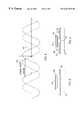
- FIG. 4is a graphical representation of a transmission signal phase shift produced by the circuit of FIG. 3 .
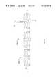
- FIG. 5is a schematic of a switched-line phase shifter in accordance with the present invention using four delay lines per stage.
- FIG. 6is a top plan view of a micro electro mechanical switch of the present invention.
- FIG. 7is a cross section of the switch in FIG. 6 taken along the section line 7 — 7 .
- FIG. 8is a cross section of the switch in FIG. 6 taken along the section line 8 — 8 .
- FIG. 9is a cross section of the switch in FIG. 6 taken along the section line 9 — 9 .
- the present inventioncomprises a phased array antenna phase shifter with one or more stages, having three or more delay lines per stage and utilizing switched-line selection of the delay lines at each stage.
- the preferred embodimentutilizes micro electro mechanical system (MEMS) technology for the switches and delay line networks within each stage, the MEMS switches used to select the desired delay line within each stage.
- MEMSmicro electro mechanical system
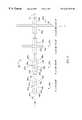
- a preferred embodiment shown in FIG. 3comprises a phase shifter 30 with four serially coupled time delay stages 32 a- 32 d.
- Phase shifter 30accepts a transmission signal on input line 40 .
- This transmission signalis generally the base carrier frequency of the antenna. Transmission of this signal by the antenna without phase shift at the radiating elements would result in a transmission beam down the antenna boresight.
- the phase shifters 30impart phase shifts in the transmission signal at each of the radiating elements.
- Input line 40is coupled to a first time delay stage 32 a of phase shifter 30 , with three delay lines 34 a- 34 c available within the stage to carry transmission signal from input line 40 .
- Each of three delay lines 34 a- 34 chave different lengths, thereby imparting different time delays to the transmission signal.
- the time delayis equivalent to the time it takes the transmission signal to transit one of three delay lines 34 a- 34 c. The longer the delay line, the greater the time delay.
- the phase of the transmission signalis shifted in proportion to the time delay.
- One of the three delay lines 34 a- 34 c in the first time delay stage 32 ais activated by closing two of six switches 36 a- 36 f to connect the selected transmission into the overall phase sifter 30 .
- Input switches 36 a- 36 cinterface between the phase shifter's input line 40 and the inputs to delay lines 34 a- 34 c, respectively, while output switches 36 d- 36 f interface between outputs of delay lines 34 a- 34 c, respectively, and the line 42 that connects the first stage 32 a and the second stage 32 b.
- one of three delay lines 34 a- 34 cis activated by closing the switches at its input and output.
- the remaining time delay stages 32 b, 32 c, 32 dare constructed and function in a manner similar to the first stage 32 a, having the same number of switches and delay lines.
- the delay lines in the first stage 32 aimpart respective phase shifts of 0°, 4.44° and 8.88°.
- the time that it takes the transmission signal to pass through the 4.44° delay line 34 cequals the time delay necessary to impart a 4.44° phase shift on the transmission signal.
- Transmission signal 44is passed through the first time delay stage 32 a along one of three delay line 34 a- 34 c closing the respective input switch 36 a- 36 c and closing the respective output switch 36 d- 36 f.
- the transmission signal 44now possessing the phase shift from first time delay stage 32 a, is coupled to the second time delay stage 32 b along line 42 .
- second time delay stage 32 badditional phase shift can be imparted on transmission signal 44 in the same manner a first time delay stage 32 a by closing the respective input and output switches within the second stage 32 b.
- the signalis coupled to third time delay stage 32 c where additional phase shift can be imparted by closing the appropriate switches in the same manner as the two previous time delay stages 32 a, 32 b.
- the signalis finally coupled from third time delay stage 32 c to fourth time delay stage 32 d where additional phase shift can be imparted.
- the transmission signal 44now having the accumulated phase shift of all time delay stages 32 a- 32 d, is coupled to radiating element 12 .
- the preferred embodiment of the present invention as embodied in FIG. 3,can shift transmission signal with a resolution of 4.44°, shifting transmission signal in increments of 4.44° through the 360° signal cycle. For instance, if a 4.44° phase shift in the transmission signal is desired, switch 36 c and switch 36 f are closed in first time delay stage 32 a and the appropriate switches within time delay stages 32 b, 32 c, 32 d are closed to impart 0° phase shift. After passing through phase shifter 30 , transmission signal will experience a 4.44° phase shift.
- switch 36 a and switch 36 d in first time delay stage 32 aare closed to activate 8.88° phase shift delay line 34 a
- switch 46 b and switch 46 b in second time delay stage 32 bare closed to activate 0° phase shift delay line 48 b
- switch 52 c and switch 52 f in third time delay stage 32 care closed to activate 39.96° phase shift delay line 54
- switch 56 c and switch 56 f in fourth time delay stage 32 dare closed to activate 239.76° delay line 58 .
- FIG. 4illustrates the transmission signal prior to phase shift 60 compared to the transmission signal after experiencing a phase shift of approximately 288.6° 62 .
- phase shifter 30has four stages 32 a- 32 d with 6 switches per stage for a total of 24 switches.
- 24 switchesare implemented in six stages 22 a- 22 f with four switches per stage. Accordingly, in a prior phase shifter 20 a transmission signal would pass through six stages and 12 switches experiencing loss and distortion at each switch.
- a transmission signalneed only encounter four stages and eight switches in passing through the phase shifter. This reduction in the number of stages results in a reduction in signal loss and distortion.
- the present inventionrealizes a greater beam steering resolution when using the same number of switches and delay lines.
- the phase shift resolution of prior art 20 shown in FIG. 2is 5.625° or 64 states through the 360° signal cycle.
- Present invention 30using the same number of switches and delay lines, has a phase shifting resolution of 4.44° or 81 states through the 360° signal cycle. This increased resolution is a result of a greater percentage of delay lines that can be dedicated to phase shifting. In the prior art 20 , half the delay lines were dedicated to zero phase shift. In the present invention 30 , only one third of the delay lines are dedicated to zero phase shift, leaving two-thirds of the delay lines to impart phase shift. This increase in the number of delay lines dedicated to phase shifting results in an increase in phase shifting resolution.
- the number of stagescan be increased.
- the preferred embodiment in FIG. 3utilizes four stages but the improvements over the prior art will be realized regardless of the number of stages. For instance, using prior art binary implementation with nine stages, results in a total of 36 switches, and 512 different phase shifting states. Using the present invention base-3 phase shifter and also using 36 switches results in six stages, and 729 states. Again, with the same number of switches, the resolution is increased while the number of stages is decreased. However, any increase in the number of switches and delay lines can result in significant increase in cost. Thus, a trade-off must be made between phase shifter resolution and phase shifter cost.
- FIG. 5shows the present invention with four delay lines per stage using the same number of switches and transmission lines as FIG. 3, but implemented with three stages 68 a-c.
- the transmission signalonly encounters six switches during transmission further reducing insertion loss and distortion.
- the optimal combination of resolution with insertion loss and distortion reductionis realized with the base-3 phase shifter.
- the physical implementation of the delay linesis similar to the delay lines as drawn in FIG. 3 and FIG. 5 .
- the delay linescan be implemented in either microstrip or coplanar waveguide forms (both planar technologies).
- the delay linescan be folded somewhat for compactness but not so close as to cause interference between the various delay lines.
- the switching network in the present inventioncan be implemented using PIN diode switches or FET switches.
- the preferred embodiment of the present inventionuses monolithically integrated switch and delay line circuit and fabrication method using MEMS technology.
- MEMS switches as described hereinare discussed in Yao and Chang, “A Surface Micromachined Miniature Switch For Telecommunication Applications with Signal Frequencies from DC up to 4 Ghz,” In Tech. Digest (1995) , pp. 384-387 and in U.S. Pat. No. 5,578,976 to Yao, which is assigned to the same assignee as the present application.
- U.S. Pat. No. 5,578,976 to Yaoalso discloses and discusses the design trade-offs in utilizing MEMS technology and the fabrication process for MEMS switches.
- the switchesare fabricated on substrate 72 using generally known micro fabrication techniques, such as masking, etching, depositation, and lift-off. Substrate 72 is then encapsulated in an IC package. Alternatively, the present invention can be packaged using a hybrid approach.
- Switch 70is attached to substrate 72 by an anchor structure 74 , which may be formed as a mesa on the substrate 72 .
- a bottom electrode 76typically connected to ground, and a signal line 78 generally comprise microstrips of a metal not easily oxidized, such as gold, for example, deposited on substrate 72 .
- Signal line 78includes a gap 79 that is opened and closed by operation of the switch as indicated by arrow 71 to activate the selected delay line.
- the actuating part of the switch 70comprises a cantilevered arm 80 , typically formed of an insulating material, such as silicon dioxide or silicon nitride.
- the cantilever arm 80forms a suspended folded-cantilever beam structure attached at one end to anchor structure 74 that extends over and above bottom electrode 76 and signal line 78 on substrate 72 .
- An electrical contact 82is positioned on the bottom side of the cantilevered arm 80 so as to face the top of substrate 72 over and above gap 19 and signal line 78 .
- a top electrode 84typically comprising a metal such as aluminum or gold, for example, are formed atop cantilever arm 80 .
- Top electrode 84starts above anchor structure 74 and extends along the top cantilever arm 80 to end at positions above the bottom electrode 76 .
- Cantilever arm 80 and top electrode 84are broadened above bottom electrode 76 to form a capacitor structure 86 .
- capacitor structure 86may be formed to include a grid of holes 88 extending through top electrode 84 and cantilever arm 80 .
- the holestypically having dimensions 1-110 ⁇ m, for example, reduce structural mass of cantilever arm 80 and the squeeze film dampening effect of air during actuation of switch 70 , as indicated by arrow 71 .
- each switch 70is normally in the “Off” position as shown in FIG. 7 .
- signal line 78is an open circuit due to gap 79 and the separation of electrical contact 82 from signal line 78 .
- Switch 70is closed to the “On” position by applying a voltage to the top electrode 84 .
- electrostatic forcesattract capacitor structure 86 (and cantilever arm 80 ) toward bottom electrode 76 .
- Actuation of cantilever arm 80 toward bottom electrode 76causes contact 82 to come into contact with signal line 78 , thereby closing gap 79 .
- This structureprovides a very low insertion loss, approximately 0.1 dB at a 4 Ghz signal frequency, and a very high isolation, approximately ⁇ 50 dB as a switching speed of approximately 1 MHZ and consumes only about 1.4 ⁇ W to switch from the off-state (open circuit) to the on-state (closed circuit) with a closure time on the order of 30 ⁇ s.
Landscapes
- Engineering & Computer Science (AREA)
- Power Engineering (AREA)
- Microelectronics & Electronic Packaging (AREA)
- Variable-Direction Aerials And Aerial Arrays (AREA)
Abstract
Description
Claims (9)
Priority Applications (1)
| Application Number | Priority Date | Filing Date | Title |
|---|---|---|---|
| US09/302,533US6281838B1 (en) | 1999-04-30 | 1999-04-30 | Base-3 switched-line phase shifter using micro electro mechanical (MEMS) technology |
Applications Claiming Priority (1)
| Application Number | Priority Date | Filing Date | Title |
|---|---|---|---|
| US09/302,533US6281838B1 (en) | 1999-04-30 | 1999-04-30 | Base-3 switched-line phase shifter using micro electro mechanical (MEMS) technology |
Publications (1)
| Publication Number | Publication Date |
|---|---|
| US6281838B1true US6281838B1 (en) | 2001-08-28 |
Family
ID=23168148
Family Applications (1)
| Application Number | Title | Priority Date | Filing Date |
|---|---|---|---|
| US09/302,533Expired - LifetimeUS6281838B1 (en) | 1999-04-30 | 1999-04-30 | Base-3 switched-line phase shifter using micro electro mechanical (MEMS) technology |
Country Status (1)
| Country | Link |
|---|---|
| US (1) | US6281838B1 (en) |
Cited By (49)
| Publication number | Priority date | Publication date | Assignee | Title |
|---|---|---|---|---|
| US20020186108A1 (en)* | 2001-04-02 | 2002-12-12 | Paul Hallbjorner | Micro electromechanical switches |
| US6650291B1 (en) | 2002-05-08 | 2003-11-18 | Rockwell Collins, Inc. | Multiband phased array antenna utilizing a unit cell |
| US6686885B1 (en)* | 2002-08-09 | 2004-02-03 | Northrop Grumman Corporation | Phased array antenna for space based radar |
| WO2004021504A1 (en)* | 2002-08-24 | 2004-03-11 | Robert Bosch Gmbh | Co-planar constant-attenuation phase modifier |
| US6741207B1 (en)* | 2000-06-30 | 2004-05-25 | Raytheon Company | Multi-bit phase shifters using MEM RF switches |
| US20040246073A1 (en)* | 2001-10-23 | 2004-12-09 | Shu-Ang Zhou | Multi-bit time delay adjuster unit for high rf applications and method |
| US20050002471A1 (en)* | 2003-07-01 | 2005-01-06 | Tramm Fred C. | Systems and methods for low loss monolithic extremely high frequency quadra-phase shift key modulation |
| US20050040874A1 (en)* | 2003-04-02 | 2005-02-24 | Allison Robert C. | Micro electro-mechanical system (mems) phase shifter |
| US20050237127A1 (en)* | 2002-06-05 | 2005-10-27 | Koninklijke Phillips Electrics N.V. | Electronic device and method of matching the impedance thereof |
| US6963117B2 (en)* | 2002-06-04 | 2005-11-08 | Electronics And Telecommunications Research Institute | Microelectromechanical device using resistive electromechanical contact |
| US20050270122A1 (en)* | 2004-03-31 | 2005-12-08 | Hyman Daniel J | Electronically controlled hybrid digital and analog phase shifter |
| US6985365B2 (en)* | 2001-09-28 | 2006-01-10 | Hewlett-Packard Development Company, L.P. | Topology for flexible and precise signal timing adjustment |
| EP1635418A1 (en)* | 2004-09-09 | 2006-03-15 | Sony Ericsson Mobile Communications AB | Phase shifter device including MEMS switches and delay lines and portable communication device using the same |
| WO2006027113A1 (en)* | 2004-09-09 | 2006-03-16 | Sony Ericsson Mobile Communication Ab | Phase shifter device including mems switches and delay lines and portable communication device using the same |
| US7068220B2 (en) | 2003-09-29 | 2006-06-27 | Rockwell Scientific Licensing, Llc | Low loss RF phase shifter with flip-chip mounted MEMS interconnection |
| US20060145921A1 (en)* | 2004-12-30 | 2006-07-06 | Microsoft Corporation | Electronically steerable sector antenna |
| US20060171357A1 (en)* | 2005-01-28 | 2006-08-03 | Microsoft Corporation | Control of a multi-sectored antenna system to improve channel efficiency |
| WO2007084071A1 (en)* | 2006-01-18 | 2007-07-26 | Åstc Aerospace Ab | Micromachined continuous time delay phase shifter |
| US7359679B2 (en) | 2005-01-28 | 2008-04-15 | Microsoft Corporation | Multi-access system and method using multi-sectored antenna |
| US20110006859A1 (en)* | 2009-07-09 | 2011-01-13 | Terry Cisco | Tunable compact time delay circuit assembly |
| WO2011034511A1 (en) | 2009-09-15 | 2011-03-24 | Mehmet Unlu | Simultaneous phase and amplitude control using triple stub topology and its implementation using rf mems technology |
| US7917255B1 (en) | 2007-09-18 | 2011-03-29 | Rockwell Colllins, Inc. | System and method for on-board adaptive characterization of aircraft turbulence susceptibility as a function of radar observables |
| EP1763151A3 (en)* | 2005-09-12 | 2013-05-29 | Delphi Delco Electronics Europe GmbH | Antenna diversity device for reception in vehicles |
| US8635765B2 (en) | 2011-06-15 | 2014-01-28 | International Business Machines Corporation | Method of forming micro-electrical-mechanical structure (MEMS) |
| EP2988371A1 (en)* | 2014-08-20 | 2016-02-24 | Huawei Technologies Co., Ltd. | Phase control method, array antenna, and system |
| US20170187086A1 (en)* | 2015-12-29 | 2017-06-29 | Synergy Microwave Corporation | Microwave mems phase shifter |
| US9712228B2 (en) | 2014-11-06 | 2017-07-18 | Ubiqomm Llc | Beam forming and pointing in a network of unmanned aerial vehicles (UAVs) for broadband access |
| RU2635875C2 (en)* | 2015-04-17 | 2017-11-16 | Акционерное общество "Федеральный научно-производственный центр "Нижегородский научно-исследовательский институт радиотехники" | Method for generating and processing of radar modified phase-shift signals |
| US9853712B2 (en)* | 2014-02-17 | 2017-12-26 | Ubiqomm Llc | Broadband access system via drone/UAV platforms |
| US9853713B2 (en) | 2016-05-06 | 2017-12-26 | Ubiqomm Llc | Unmanned aerial vehicle (UAV) beam pointing and data rate optimization for high throughput broadband access |
| US9853715B2 (en)* | 2014-02-17 | 2017-12-26 | Ubiqomm Llc | Broadband access system via drone/UAV platforms |
| US9859972B2 (en) | 2014-02-17 | 2018-01-02 | Ubiqomm Llc | Broadband access to mobile platforms using drone/UAV background |
| EP3336965A1 (en)* | 2016-12-16 | 2018-06-20 | Industrial Technology Research Institute | Space-fed active phased antenna array |
| US10033349B2 (en)* | 2016-02-05 | 2018-07-24 | Psemi Corporation | Low loss multi-state phase shifter |
| US10103803B2 (en) | 2015-05-13 | 2018-10-16 | Bridgewest Finance Llc | Ground terminal and gateway beam pointing toward an unmanned aerial vehicle (UAV) for network access |
| US10153829B2 (en) | 2015-05-13 | 2018-12-11 | Bridgewest Finance Llc | Ground terminal and UAV beam pointing in an unmanned aerial vehicle (UAV) for network access |
| US10181893B2 (en) | 2014-10-16 | 2019-01-15 | Bridgewest Finance Llc | Unmanned aerial vehicle (UAV) beam forming and pointing toward ground coverage area cells for broadband access |
| US10313686B2 (en) | 2016-09-20 | 2019-06-04 | Gopro, Inc. | Apparatus and methods for compressing video content using adaptive projection selection |
| US10325742B2 (en) | 2015-12-29 | 2019-06-18 | Synergy Microwave Corporation | High performance switch for microwave MEMS |
| US10326200B2 (en)* | 2017-10-18 | 2019-06-18 | General Electric Company | High impedance RF MEMS transmission devices and method of making the same |
| US10530323B2 (en)* | 2017-06-22 | 2020-01-07 | Huawei Technologies Co., Ltd. | Methods and apparatus of adjusting delays of signals |
| US10594030B2 (en)* | 2017-02-01 | 2020-03-17 | General Electric Company | True time delay module and beam former having plural delay lines selectively connected by plural switching elements including one or more intermediate switching element |
| KR20200057091A (en)* | 2017-10-13 | 2020-05-25 | 제네럴 일렉트릭 컴퍼니 | Real-time delay beamformer and its operation method |
| US10763827B1 (en) | 2019-08-29 | 2020-09-01 | Nxp B.V. | Delay line with controllable phase-shifting cells |
| US10763594B1 (en)* | 2019-02-11 | 2020-09-01 | Wistron Corp. | Antenna system |
| US10784066B2 (en) | 2017-03-10 | 2020-09-22 | Synergy Microwave Corporation | Microelectromechanical switch with metamaterial contacts |
| US12166254B2 (en)* | 2021-01-26 | 2024-12-10 | Beijing Boe Technology Development Co., Ltd. | Phase shifter with at least one phase shifting unit having film bridges and connection electrodes for connecting adjacent signal line segments |
| US12206376B2 (en) | 2017-01-24 | 2025-01-21 | Psemi Corporation | Glitch mitigation in switched reactance phase shifters |
| CN119363086A (en)* | 2024-10-31 | 2025-01-24 | 西安电子科技大学 | A channel selection switch, a 90-degree terahertz phase shifter and a phased array radar |
Citations (7)
| Publication number | Priority date | Publication date | Assignee | Title |
|---|---|---|---|---|
| US2407169A (en)* | 1941-05-26 | 1946-09-03 | Hazeltine Research Inc | System for locating radiated-signal reflectors |
| US3781722A (en)* | 1973-03-12 | 1973-12-25 | Rca Corp | Digitally variable delay time system |
| US4649393A (en) | 1984-02-17 | 1987-03-10 | The United States Of America As Represented By The Secretary Of The Army | Phased array antennas with binary phase shifters |
| US5424696A (en)* | 1992-05-08 | 1995-06-13 | Mitsubishi Denki Kabushiki Kaisha | Switched line phase shifter |
| US5578976A (en) | 1995-06-22 | 1996-11-26 | Rockwell International Corporation | Micro electromechanical RF switch |
| US5646568A (en)* | 1995-02-28 | 1997-07-08 | Ando Electric Co., Ltd. | Delay circuit |
| US6091311A (en)* | 1997-08-21 | 2000-07-18 | The United States Of America As Represented By The Secretary Of The Navy | Selectable path stripline/slotline digital phase shifter |
- 1999
- 1999-04-30USUS09/302,533patent/US6281838B1/ennot_activeExpired - Lifetime
Patent Citations (7)
| Publication number | Priority date | Publication date | Assignee | Title |
|---|---|---|---|---|
| US2407169A (en)* | 1941-05-26 | 1946-09-03 | Hazeltine Research Inc | System for locating radiated-signal reflectors |
| US3781722A (en)* | 1973-03-12 | 1973-12-25 | Rca Corp | Digitally variable delay time system |
| US4649393A (en) | 1984-02-17 | 1987-03-10 | The United States Of America As Represented By The Secretary Of The Army | Phased array antennas with binary phase shifters |
| US5424696A (en)* | 1992-05-08 | 1995-06-13 | Mitsubishi Denki Kabushiki Kaisha | Switched line phase shifter |
| US5646568A (en)* | 1995-02-28 | 1997-07-08 | Ando Electric Co., Ltd. | Delay circuit |
| US5578976A (en) | 1995-06-22 | 1996-11-26 | Rockwell International Corporation | Micro electromechanical RF switch |
| US6091311A (en)* | 1997-08-21 | 2000-07-18 | The United States Of America As Represented By The Secretary Of The Navy | Selectable path stripline/slotline digital phase shifter |
Non-Patent Citations (2)
| Title |
|---|
| M.I. Skolnik, "Radar Handbook"; McGraw-Hill Book Company; New York, 1980 (second edition); pp. 286-288.* |
| Skolnik, "Phased Array Radar Antennas", Radar Handbook, Second Edition, pp. 7.63-7.68, (1990); McGraw-Hill; New York. |
Cited By (74)
| Publication number | Priority date | Publication date | Assignee | Title |
|---|---|---|---|---|
| US6741207B1 (en)* | 2000-06-30 | 2004-05-25 | Raytheon Company | Multi-bit phase shifters using MEM RF switches |
| US20020186108A1 (en)* | 2001-04-02 | 2002-12-12 | Paul Hallbjorner | Micro electromechanical switches |
| US6985365B2 (en)* | 2001-09-28 | 2006-01-10 | Hewlett-Packard Development Company, L.P. | Topology for flexible and precise signal timing adjustment |
| US7053732B2 (en)* | 2001-10-23 | 2006-05-30 | Telefonaktiebolaget Lm Ericsson (Publ) | Multi-bit time delay adjuster unit for high RF applications and method |
| US20040246073A1 (en)* | 2001-10-23 | 2004-12-09 | Shu-Ang Zhou | Multi-bit time delay adjuster unit for high rf applications and method |
| US6650291B1 (en) | 2002-05-08 | 2003-11-18 | Rockwell Collins, Inc. | Multiband phased array antenna utilizing a unit cell |
| US6963117B2 (en)* | 2002-06-04 | 2005-11-08 | Electronics And Telecommunications Research Institute | Microelectromechanical device using resistive electromechanical contact |
| US20050237127A1 (en)* | 2002-06-05 | 2005-10-27 | Koninklijke Phillips Electrics N.V. | Electronic device and method of matching the impedance thereof |
| US20090015346A1 (en)* | 2002-06-05 | 2009-01-15 | Van Delden Martinus Hermanus W | Electronic device and method of matching the impedance thereof |
| US7586387B2 (en)* | 2002-06-05 | 2009-09-08 | Nxp B.V. | Electronic device and method of matching the impedance thereof |
| US7893790B2 (en) | 2002-06-05 | 2011-02-22 | Nxp B.V. | Electronic device and method of matching the impedance thereof |
| US6686885B1 (en)* | 2002-08-09 | 2004-02-03 | Northrop Grumman Corporation | Phased array antenna for space based radar |
| US20050012564A1 (en)* | 2002-08-24 | 2005-01-20 | Joerg Schoebel | Co-planar constant-attenuation phase modifier |
| WO2004021504A1 (en)* | 2002-08-24 | 2004-03-11 | Robert Bosch Gmbh | Co-planar constant-attenuation phase modifier |
| US20050040874A1 (en)* | 2003-04-02 | 2005-02-24 | Allison Robert C. | Micro electro-mechanical system (mems) phase shifter |
| US6958665B2 (en) | 2003-04-02 | 2005-10-25 | Raytheon Company | Micro electro-mechanical system (MEMS) phase shifter |
| US20050002471A1 (en)* | 2003-07-01 | 2005-01-06 | Tramm Fred C. | Systems and methods for low loss monolithic extremely high frequency quadra-phase shift key modulation |
| US7068220B2 (en) | 2003-09-29 | 2006-06-27 | Rockwell Scientific Licensing, Llc | Low loss RF phase shifter with flip-chip mounted MEMS interconnection |
| US20050270122A1 (en)* | 2004-03-31 | 2005-12-08 | Hyman Daniel J | Electronically controlled hybrid digital and analog phase shifter |
| US7355492B2 (en)* | 2004-03-31 | 2008-04-08 | Xcom Wireless | Electronically controlled hybrid digital and analog phase shifter |
| WO2006027113A1 (en)* | 2004-09-09 | 2006-03-16 | Sony Ericsson Mobile Communication Ab | Phase shifter device including mems switches and delay lines and portable communication device using the same |
| EP1635418A1 (en)* | 2004-09-09 | 2006-03-15 | Sony Ericsson Mobile Communications AB | Phase shifter device including MEMS switches and delay lines and portable communication device using the same |
| US20060145921A1 (en)* | 2004-12-30 | 2006-07-06 | Microsoft Corporation | Electronically steerable sector antenna |
| US7397425B2 (en)* | 2004-12-30 | 2008-07-08 | Microsoft Corporation | Electronically steerable sector antenna |
| US7359679B2 (en) | 2005-01-28 | 2008-04-15 | Microsoft Corporation | Multi-access system and method using multi-sectored antenna |
| US20060171357A1 (en)* | 2005-01-28 | 2006-08-03 | Microsoft Corporation | Control of a multi-sectored antenna system to improve channel efficiency |
| US7359362B2 (en) | 2005-01-28 | 2008-04-15 | Microsoft Corporation | Control of a multi-sectored antenna system to improve channel efficiency |
| EP1763151A3 (en)* | 2005-09-12 | 2013-05-29 | Delphi Delco Electronics Europe GmbH | Antenna diversity device for reception in vehicles |
| WO2007084071A1 (en)* | 2006-01-18 | 2007-07-26 | Åstc Aerospace Ab | Micromachined continuous time delay phase shifter |
| US7917255B1 (en) | 2007-09-18 | 2011-03-29 | Rockwell Colllins, Inc. | System and method for on-board adaptive characterization of aircraft turbulence susceptibility as a function of radar observables |
| US8264300B2 (en)* | 2009-07-09 | 2012-09-11 | Raytheon Company | Tunable transmission line time delay circuit having conductive floating strip segments connected by switches |
| US20110006859A1 (en)* | 2009-07-09 | 2011-01-13 | Terry Cisco | Tunable compact time delay circuit assembly |
| WO2011034511A1 (en) | 2009-09-15 | 2011-03-24 | Mehmet Unlu | Simultaneous phase and amplitude control using triple stub topology and its implementation using rf mems technology |
| US8635765B2 (en) | 2011-06-15 | 2014-01-28 | International Business Machines Corporation | Method of forming micro-electrical-mechanical structure (MEMS) |
| US9786459B2 (en) | 2011-06-15 | 2017-10-10 | International Business Machines Corporation | Normally closed microelectromechanical switches (MEMS), methods of manufacture and design structures |
| US9343255B2 (en) | 2011-06-15 | 2016-05-17 | International Business Machines Corporation | Normally closed microelectromechanical switches (MEMS), methods of manufacture and design structures |
| US9859972B2 (en) | 2014-02-17 | 2018-01-02 | Ubiqomm Llc | Broadband access to mobile platforms using drone/UAV background |
| US9853715B2 (en)* | 2014-02-17 | 2017-12-26 | Ubiqomm Llc | Broadband access system via drone/UAV platforms |
| US9853712B2 (en)* | 2014-02-17 | 2017-12-26 | Ubiqomm Llc | Broadband access system via drone/UAV platforms |
| CN105450200A (en)* | 2014-08-20 | 2016-03-30 | 华为技术有限公司 | Phase control method, array antenna, and phase control system |
| EP2988371A1 (en)* | 2014-08-20 | 2016-02-24 | Huawei Technologies Co., Ltd. | Phase control method, array antenna, and system |
| US9419833B2 (en) | 2014-08-20 | 2016-08-16 | Huawei Technologies Co., Ltd. | Phase control method, array antenna, and system |
| US10181893B2 (en) | 2014-10-16 | 2019-01-15 | Bridgewest Finance Llc | Unmanned aerial vehicle (UAV) beam forming and pointing toward ground coverage area cells for broadband access |
| US9712228B2 (en) | 2014-11-06 | 2017-07-18 | Ubiqomm Llc | Beam forming and pointing in a network of unmanned aerial vehicles (UAVs) for broadband access |
| US9800320B2 (en) | 2014-11-06 | 2017-10-24 | Ubiqomm Llc | Beam forming and pointing in a network of unmanned aerial vehicles (UAVs) for broadband access |
| US9866312B2 (en) | 2014-11-06 | 2018-01-09 | Ubiqomm Llc | Beam forming and pointing in a network of unmanned aerial vehicles (UAVs) for broadband access |
| RU2635875C2 (en)* | 2015-04-17 | 2017-11-16 | Акционерное общество "Федеральный научно-производственный центр "Нижегородский научно-исследовательский институт радиотехники" | Method for generating and processing of radar modified phase-shift signals |
| US10103803B2 (en) | 2015-05-13 | 2018-10-16 | Bridgewest Finance Llc | Ground terminal and gateway beam pointing toward an unmanned aerial vehicle (UAV) for network access |
| US10153829B2 (en) | 2015-05-13 | 2018-12-11 | Bridgewest Finance Llc | Ground terminal and UAV beam pointing in an unmanned aerial vehicle (UAV) for network access |
| US10325742B2 (en) | 2015-12-29 | 2019-06-18 | Synergy Microwave Corporation | High performance switch for microwave MEMS |
| US20170187086A1 (en)* | 2015-12-29 | 2017-06-29 | Synergy Microwave Corporation | Microwave mems phase shifter |
| US10199703B2 (en)* | 2015-12-29 | 2019-02-05 | Synergy Microwave Corporation | Phase shifter comprised of plural coplanar waveguides connected by switches having cantilever beams and mechanical springs |
| JP2017126981A (en)* | 2015-12-29 | 2017-07-20 | シナジー マイクロウェーブ コーポレーションSynergy Microwave Corporation | Microwave MEMS phase shifter |
| US10033349B2 (en)* | 2016-02-05 | 2018-07-24 | Psemi Corporation | Low loss multi-state phase shifter |
| US9853713B2 (en) | 2016-05-06 | 2017-12-26 | Ubiqomm Llc | Unmanned aerial vehicle (UAV) beam pointing and data rate optimization for high throughput broadband access |
| US9980267B2 (en) | 2016-05-06 | 2018-05-22 | Bridgewest Finance Llc | Unmanned aerial vehicle (UAV) beam pointing and data rate optimization for high throughput broadband access |
| US10321461B2 (en) | 2016-05-06 | 2019-06-11 | Bridgewest Finance Llc | Unmanned aerial vehicle (UAV) beam pointing and data rate optimization for high throughput broadband access |
| US10313686B2 (en) | 2016-09-20 | 2019-06-04 | Gopro, Inc. | Apparatus and methods for compressing video content using adaptive projection selection |
| US10757423B2 (en) | 2016-09-20 | 2020-08-25 | Gopro, Inc. | Apparatus and methods for compressing video content using adaptive projection selection |
| EP3336965A1 (en)* | 2016-12-16 | 2018-06-20 | Industrial Technology Research Institute | Space-fed active phased antenna array |
| US12206376B2 (en) | 2017-01-24 | 2025-01-21 | Psemi Corporation | Glitch mitigation in switched reactance phase shifters |
| US10594030B2 (en)* | 2017-02-01 | 2020-03-17 | General Electric Company | True time delay module and beam former having plural delay lines selectively connected by plural switching elements including one or more intermediate switching element |
| US10784066B2 (en) | 2017-03-10 | 2020-09-22 | Synergy Microwave Corporation | Microelectromechanical switch with metamaterial contacts |
| US10530323B2 (en)* | 2017-06-22 | 2020-01-07 | Huawei Technologies Co., Ltd. | Methods and apparatus of adjusting delays of signals |
| KR102514959B1 (en)* | 2017-10-13 | 2023-03-27 | 제네럴 일렉트릭 컴퍼니 | Real-time delayed beamformer and its operating method |
| JP2020537440A (en)* | 2017-10-13 | 2020-12-17 | ゼネラル・エレクトリック・カンパニイ | Real time delay beam former and how it works |
| EP3695528A4 (en)* | 2017-10-13 | 2021-07-21 | General Electric Company | BEAM FORMER WITH REAL-TIME DELAY AND OPERATING PROCEDURES |
| KR20200057091A (en)* | 2017-10-13 | 2020-05-25 | 제네럴 일렉트릭 컴퍼니 | Real-time delay beamformer and its operation method |
| CN111226347A (en)* | 2017-10-18 | 2020-06-02 | 通用电气公司 | High impedance RF MEMS transmission device and method of manufacturing the same |
| US10326200B2 (en)* | 2017-10-18 | 2019-06-18 | General Electric Company | High impedance RF MEMS transmission devices and method of making the same |
| US10763594B1 (en)* | 2019-02-11 | 2020-09-01 | Wistron Corp. | Antenna system |
| US10763827B1 (en) | 2019-08-29 | 2020-09-01 | Nxp B.V. | Delay line with controllable phase-shifting cells |
| US12166254B2 (en)* | 2021-01-26 | 2024-12-10 | Beijing Boe Technology Development Co., Ltd. | Phase shifter with at least one phase shifting unit having film bridges and connection electrodes for connecting adjacent signal line segments |
| CN119363086A (en)* | 2024-10-31 | 2025-01-24 | 西安电子科技大学 | A channel selection switch, a 90-degree terahertz phase shifter and a phased array radar |
Similar Documents
| Publication | Publication Date | Title |
|---|---|---|
| US6281838B1 (en) | Base-3 switched-line phase shifter using micro electro mechanical (MEMS) technology | |
| JP7025838B2 (en) | Phase shifter and phased array | |
| US7068220B2 (en) | Low loss RF phase shifter with flip-chip mounted MEMS interconnection | |
| US6624720B1 (en) | Micro electro-mechanical system (MEMS) transfer switch for wideband device | |
| Brown | RF-MEMS switches for reconfigurable integrated circuits | |
| US6016092A (en) | Miniature electromagnetic microwave switches and switch arrays | |
| EP0840394B1 (en) | Ultrabroadband, adaptive phased array antenna systems using microelectromechanical electromagnetic components | |
| WO2001013457A1 (en) | Electrical switches | |
| US6535091B2 (en) | Microelectronic mechanical systems (MEMS) switch and method of fabrication | |
| CA2374131C (en) | Multi-bit phase shifters using mem rf switches | |
| US6133807A (en) | High-frequency switch and integrated high-frequency switch array | |
| US7898371B2 (en) | Electromechanical switch with partially rigidified electrode | |
| US7477884B2 (en) | Tri-state RF switch | |
| WO2002079079A1 (en) | Micro electromechanical switches | |
| WO2002045203A1 (en) | Fluidic self-assembly of active antenna | |
| JPH0795647B2 (en) | Improved miniature microwave and millimeter wave tunable circuit | |
| US7157993B2 (en) | 1:N MEM switch module | |
| EP0892419B1 (en) | Micro electro-mechanical system (MEMS) switch | |
| Suzuki et al. | A micromachined RF microswitch applicable to phased-array antennas | |
| EP1573769B1 (en) | Microelectromechanical rf switch | |
| US6191754B1 (en) | Antenna system using time delays with mercury wetted switches | |
| US6750999B1 (en) | Reconfigurable quasi-optical unit cells | |
| WO2000077543A1 (en) | Reconfigurable quasi-optical unit cells | |
| JPH0748603B2 (en) | Semiconductor phase shifter | |
| WO2002069023A2 (en) | Variable time delay microwave transmission line |
Legal Events
| Date | Code | Title | Description |
|---|---|---|---|
| AS | Assignment | Owner name:ROCKWELL SCIENCE CENTER, LLC, CALIFORNIA Free format text:ASSIGNMENT OF ASSIGNORS INTEREST;ASSIGNOR:HONG, JOHN H.;REEL/FRAME:009931/0344 Effective date:19990423 | |
| STCF | Information on status: patent grant | Free format text:PATENTED CASE | |
| REMI | Maintenance fee reminder mailed | ||
| FPAY | Fee payment | Year of fee payment:4 | |
| SULP | Surcharge for late payment | ||
| AS | Assignment | Owner name:INNOVATIVE TECHNOLOGY LICENSING, LLC, CALIFORNIA Free format text:CHANGE OF NAME;ASSIGNOR:ROCKWELL TECHNOLOGIES, LLC;REEL/FRAME:018160/0240 Effective date:20010628 Owner name:ROCKWELL TECHNOLOGIES, LLC, CALIFORNIA Free format text:ASSIGNMENT OF ASSIGNORS INTEREST;ASSIGNOR:ROCKWELL SCIENCE CENTER, LLC;REEL/FRAME:018160/0122 Effective date:20000330 Owner name:ROCKWELL SCIENTIFIC LICENSING, LLC, CALIFORNIA Free format text:CHANGE OF NAME;ASSIGNOR:INNOVATIVE TECHNOLOGY LICENSING, LLC;REEL/FRAME:018160/0250 Effective date:20030919 | |
| AS | Assignment | Owner name:TELEDYNE LICENSING, LLC, CALIFORNIA Free format text:CHANGE OF NAME;ASSIGNOR:ROCKWELL SCIENTIFIC LICENSING, LLC;REEL/FRAME:018573/0649 Effective date:20060918 | |
| FPAY | Fee payment | Year of fee payment:8 | |
| AS | Assignment | Owner name:TELEDYNE SCIENTIFIC & IMAGING, LLC, CALIFORNIA Free format text:MERGER;ASSIGNOR:TELEDYNE LICENSING, LLC;REEL/FRAME:027830/0206 Effective date:20111221 | |
| FPAY | Fee payment | Year of fee payment:12 |