US6281590B1 - Circuit and method for providing interconnections among individual integrated circuit chips in a multi-chip module - Google Patents
Circuit and method for providing interconnections among individual integrated circuit chips in a multi-chip moduleDownload PDFInfo
- Publication number
- US6281590B1 US6281590B1US08/838,536US83853697AUS6281590B1US 6281590 B1US6281590 B1US 6281590B1US 83853697 AUS83853697 AUS 83853697AUS 6281590 B1US6281590 B1US 6281590B1
- Authority
- US
- United States
- Prior art keywords
- chip
- separate
- circuit
- mcm
- circuit portion
- Prior art date
- Legal status (The legal status is an assumption and is not a legal conclusion. Google has not performed a legal analysis and makes no representation as to the accuracy of the status listed.)
- Expired - Lifetime, expires
Links
Images
Classifications
- H—ELECTRICITY
- H01—ELECTRIC ELEMENTS
- H01L—SEMICONDUCTOR DEVICES NOT COVERED BY CLASS H10
- H01L23/00—Details of semiconductor or other solid state devices
- H01L23/48—Arrangements for conducting electric current to or from the solid state body in operation, e.g. leads, terminal arrangements ; Selection of materials therefor
- H01L23/50—Arrangements for conducting electric current to or from the solid state body in operation, e.g. leads, terminal arrangements ; Selection of materials therefor for integrated circuit devices, e.g. power bus, number of leads
- H—ELECTRICITY
- H01—ELECTRIC ELEMENTS
- H01L—SEMICONDUCTOR DEVICES NOT COVERED BY CLASS H10
- H01L23/00—Details of semiconductor or other solid state devices
- H01L23/52—Arrangements for conducting electric current within the device in operation from one component to another, i.e. interconnections, e.g. wires, lead frames
- H01L23/538—Arrangements for conducting electric current within the device in operation from one component to another, i.e. interconnections, e.g. wires, lead frames the interconnection structure between a plurality of semiconductor chips being formed on, or in, insulating substrates
- H01L23/5386—Geometry or layout of the interconnection structure
- H—ELECTRICITY
- H01—ELECTRIC ELEMENTS
- H01L—SEMICONDUCTOR DEVICES NOT COVERED BY CLASS H10
- H01L25/00—Assemblies consisting of a plurality of semiconductor or other solid state devices
- H01L25/03—Assemblies consisting of a plurality of semiconductor or other solid state devices all the devices being of a type provided for in a single subclass of subclasses H10B, H10D, H10F, H10H, H10K or H10N, e.g. assemblies of rectifier diodes
- H01L25/04—Assemblies consisting of a plurality of semiconductor or other solid state devices all the devices being of a type provided for in a single subclass of subclasses H10B, H10D, H10F, H10H, H10K or H10N, e.g. assemblies of rectifier diodes the devices not having separate containers
- H01L25/065—Assemblies consisting of a plurality of semiconductor or other solid state devices all the devices being of a type provided for in a single subclass of subclasses H10B, H10D, H10F, H10H, H10K or H10N, e.g. assemblies of rectifier diodes the devices not having separate containers the devices being of a type provided for in group H10D89/00
- H01L25/0655—Assemblies consisting of a plurality of semiconductor or other solid state devices all the devices being of a type provided for in a single subclass of subclasses H10B, H10D, H10F, H10H, H10K or H10N, e.g. assemblies of rectifier diodes the devices not having separate containers the devices being of a type provided for in group H10D89/00 the devices being arranged next to each other
- H—ELECTRICITY
- H01—ELECTRIC ELEMENTS
- H01L—SEMICONDUCTOR DEVICES NOT COVERED BY CLASS H10
- H01L2924/00—Indexing scheme for arrangements or methods for connecting or disconnecting semiconductor or solid-state bodies as covered by H01L24/00
- H01L2924/0001—Technical content checked by a classifier
- H01L2924/0002—Not covered by any one of groups H01L24/00, H01L24/00 and H01L2224/00
Definitions
- the present inventionis directed, in general, to integrated circuits and, more specifically, to a circuit and method for providing interconnections among individual integrated circuit (“IC”) chips in a multi-chip module (“MCM”).
- ICintegrated circuit
- MCMmulti-chip module
- Integrated circuitsare the tiny “chips,” usually less than 0.5′′ on a side, of silicon (or other similar material) on which is patterned the transistors and interconnections that make modem electronic systems do what they do; compute, amplify, etc.
- IC fabrication processesMany advances in IC fabrication processes have brought about dramatic increases in the number of transistors that can be fabricated on each chip, thereby increasing the capabilities, as well as decreasing the size of ICs and, thus, the size of devices using ICs. Whereas the actual size of a typical IC is much less than the size of a conventional IC package, novel IC packaging designs that can significantly reduce the size of electronic devices are being explored.
- device packagingbecomes a major limitation on system speed.
- IC packagesconsist of the same basic elements: the IC, a lead frame, wire bonds, and an encapsulant.
- the lead frameis connected to the IC using a very thin wire bonded to both the chip and the lead frame.
- the encapsulant or moldingusually made from plastic, forms a package that encloses the IC, wire bonds, and part of the lead frame, thereby protecting the IC from the ambient environment.
- An electronic systemis typically constructed from multiple packaged IC devices, which are electrically- and physically-coupled to a printing circuit board (“PCB”) by leads that form a portion of the lead frame and which extend from the IC package; the PCB including metallic traces for interconnecting the multiple ICs.
- a relatively new approach to packagingis to place more than one IC in the same package; the multiple IC package is called a Multi-Chip Module (“MCM”), or a “hybrid” package.
- MCMMulti-Chip Module
- MCM packagesare similar to conventional single-chip package designs. MCM packages, however, house more than one IC by mounting conventional chips on a common substrate, which has metallic paths formed thereon that interconnect the individual chips. A conventional lead frame is connected to terminals on the substrate using a very thin wire, and the substrate and lead frame are then enclosed by an encapsulant to form a protective package.
- MCMsmay play an important role in furthering that objective by eliminating a level of packaging for many components, facilitating the integration of multiple analog and digital technologies in a single module, reducing electromagnetic interference (“EMI”) problems, and increasing the input/output (“I/O”) capabilities per chip.
- EMIelectromagnetic interference
- I/Oinput/output
- chip-to-chip wiring within a MCMis cheaper and faster than PCB wiring and reduces the board area needed for a device.
- the capabilities of ICs designed for conventional single chip packagesis reduced due to a desire to reduce the package size, which necessarily requires reducing the number of package leads.
- an ICmay process data internally using a plural-conductor (i.e., “parallel”) bus, the data may be serialized such that it can be communicated to another IC through only one lead.
- MCMplural-conductor
- a principle advantage of MCMsis the capability to integrate many ICs in one package, that advantage is partially diminished if it is necessary to design ICs specifically for use in MCMs, rather than using ICs designed for conventional single-chip packages.
- the MCMincludes: (1) a substrate for supporting a plurality of separate integrated circuit (IC) chips thereon, (2) first and second separate IC chips mounted on the substrate, the first separate IC chip including first and second circuit portions coupled together by at least one signal conductor, and (3) interconnecting means that directly couples at least one signal conductor of the first separate IC chip to the second separate IC chip, the interconnecting means bypassing the second circuit portion of the first separate IC chip.
- ICintegrated circuit
- the present inventiontherefore introduces the broad concept of bypassing circuit portions associated with existing IC chips, when used in an MCM, by providing an interconnecting means that directly couples signal conductors within one IC to another IC within the MCM, rather than using the conventional bonding pads used when an IC is separately-packaged.
- an interconnecting meansthat directly couples signal conductors within one IC to another IC within the MCM, rather than using the conventional bonding pads used when an IC is separately-packaged.
- the interconnecting meansdirectly couples at least one signal conductor of one IC to a conventional bonding pad of a second IC.
- the second IC chipalso includes first and second circuit portions coupled together by at least one signal conductor, and the interconnecting means directly couples at least one signal conductor of the first IC chip to at least one signal conductor of the second IC chip, thereby completely bypassing the conventional bonding pads of both the first and second IC chips.
- the internal signal conductors of the ICsare directly coupled together to form a trans-IC bus that spans the MCM.
- the interconnecting meansmay selectively-bypass conventional bonding pads and/or circuit portions associated with conventional and existing IC chips. In this manner, conventional and existing IC chips may be suitably employed in conventional single-IC packages, as well as MCMs, without modification thereto.
- the circuit portions of one or both ICs which are bypassedmay be decoupled from a source of electrical power. While not necessary to the broad scope of the present invention, disabling the power to one or more of the circuit portions decreases overall power consumption by the MCM.
- a first circuit portion of each of the IC chipsis a clock driver circuit for providing a clock signal to a second circuit portion of each of the IC chips, the interconnecting means bypassing the clock driver of one of the IC chips whereby the second circuit portion of that IC chip receives the clock signal from the clock driver of the other IC chip.
- a first IC chipincludes a plural-conductor bus and a circuit portion that includes a multiplexing circuit and an output buffer, the interconnecting means directly coupling to the plural-conductor bus to thereby bypass the multiplexing circuit and output buffer of the first IC chip.
- a second IC chipincludes a plural-conductor bus and a circuit portion that includes an input buffer and a demultiplexing circuit, the interconnecting means directly coupling to the plural-conductor bus to thereby bypass the input buffer and the demultiplexing circuit of the second IC chip.
- the related embodimentsprovide a means of bypassing the circuits necessary to serialize data communications between the ICs when the ICs are separately-packaged; the interconnecting means providing a trans-IC plural-conductor bus that spans the MCM, whereby the transmission efficiency of data between the separate ICs may be improved when employed in an MCM.
- FIG. 1illustrates an exemplary interconnection of separately-packaged integrated circuits (“IC”s) on a printed circuit board (“PCB”); and
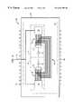
- FIG. 2illustrates an exemplary multi-chip module (MCM) including an exemplary interconnection of individual ICs according to the principles of the present invention.
- MCMmulti-chip module
- ICs 110 , 120are generally illustrated as including exemplary ICs 111 and 121 , respectively, which are coupled to lead frames having a plurality of leads, generally designated as 130 , which are enclosed by protective packages, generally designated as 140 .; those skilled in the art are familiar with the techniques of coupling a lead frame to “bonding pads” (not shown) on an IC.
- Exemplary ICs 111 and 121include signal processing circuitry 112 and 122 (or “first circuit portions”), respectively, which may be analog or digital, or a hybrid thereof. In order to share data between ICs, exemplary ICs 111 and 121 further include plural-conductor IC buses 113 and 123 , respectively; those skilled in the art are familiar with the use of plural-conductor, or “parallel,” buses to share data between electrical circuits.
- exemplary ICs 111 and 121further include serial input/output (“I/O”) “ports” (or “second circuit portions”) coupled to the plural-conductor IC buses 113 , 123 .
- the serial port of exemplary IC 111is generally illustrated as an output port and includes a multiplexer 114 and an output buffer 115 ;
- the serial port of exemplary IC 121is generally illustrated as an input port and includes an input buffer 125 and a demultiplexer 124 .
- the output buffer 115 of exemplary IC 111is coupled, via a bonding pad (not shown), to lead 130 - 6 of conventionally-packaged IC 110 , and the input buffer 125 of exemplary IC 121 is coupled, via a bonding pad (not shown), to lead 130 - 7 of conventionally-packaged IC 120 ; the leads 130 - 6 and 130 - 7 are interconnected by a metallic path 101 on PCB 100 , whereby data can be communicated from exemplary IC 111 to exemplary IC 121 . Because of the parallel to serial conversion of the data to be transmitted between exemplary ICs 111 and 121 , there may be a loss in the efficiency of data transmission. The loss in transmission efficiency, however, is often considered an acceptable trade-off for a reduced package size, which is made possible by using a single lead (e.g., leads 130 - 6 , 130 - 7 ) on each IC for data I/O.
- Electrical poweris provided to exemplary conventionally-packaged ICs 10 and 120 by coupling a voltage source 150 to leads 130 - 1 , 130 - 2 , and a ground reference to leads 1303 , 130 - 4 , respectively.
- the electrical poweris coupled to signal processing circuitry 112 , multiplexer 114 and output buffer 115 by a power bus 116 on exemplary IC 111 ; and to signal processing circuitry 122 , input buffer 125 and demultiplexer 124 by a power bus 126 on exemplary IC 121 .
- MCM 200includes a substrate 210 for supporting a plurality of individual IC chips, such as exemplary ICs 111 , 121 mounted on the substrate; the substrate 210 having metallic paths formed thereon that interconnect the individual ICs.
- a conventional lead frame(not shown) is connected to bonding pads (not shown) on the substrate 210 using a very thin wire, and the substrate 210 and lead frame are then enclosed by an encapsulant to form a protective package 220 having a plurality of leads, generally designated as 230 , extending therefrom.
- the present inventionintroduces a circuit and method for integrating exemplary ICs 111 and 121 into exemplary MCM 200 , whereby the efficiency of data communications between the ICs is improved and the total power dissipation is reduced.
- exemplary ICs 111 , 121are integrated onto a common substrate 210 , there is no need to serialize the data associated with plural-conductor buses 113 and 123 , as illustrated in FIG. 1; i.e., internal to exemplary MCM 200 , there is no need to be concerned with reducing the number of signal paths because there are no package leads interposed between the exemplary ICs 111 , 121 .
- exemplary MCM 200further includes a plural-conductor interconnecting bus 230 (or “interconnecting means”) that couples the plural-conductor IC bus 113 of exemplary IC 111 to the plural-conductor IC bus 123 of exemplary IC 121 , thereby bypassing the multiplexing circuits and buffers of exemplary ICs 111 and 121 and eliminating signal latency associated therewith.
- a plural-conductor interconnecting bus 230(or “interconnecting means”) that couples the plural-conductor IC bus 113 of exemplary IC 111 to the plural-conductor IC bus 123 of exemplary IC 121 , thereby bypassing the multiplexing circuits and buffers of exemplary ICs 111 and 121 and eliminating signal latency associated therewith.
- the plural-conductor IC bus 113is partially comprised of metallic paths formed on substrate 210 and partially comprised of wire leads that couple individual bus conductors of plural-conductor IC buses 123 , 121 to corresponding metallic paths formed on substrate 210 ; alternatively, the plural-conductor interconnecting bus 230 may be solely comprised of wire leads that directly couple individual bus conductors of plural-conductor IC bus 113 to corresponding individual bus conductors of plural-conductor IC bus 123 .
- the present inventiontherefore introduces the broad concept of bypassing, for example, multiplexing circuits (e.g., multiplexer 114 and demultiplexer 124 ) and buffers (e.g., output buffer 115 and input buffer 125 ) associated with existing serial ports on IC chips by providing a plural-conductor (parallel) interconnecting bus to span the plural-conductor IC buses directly. Signal latency (delay) associated with the multiplexing circuits and the buffers are avoided, thereby increasing the overall signal processing speed of the MCM.
- multiplexing circuitse.g., multiplexer 114 and demultiplexer 124
- bufferse.g., output buffer 115 and input buffer 125
- the principles of the present inventionare not limited, however, to only bypassing multiplexing and buffer circuits; the principles of the present invention may be applied to bypass any circuit portion of an IC, when used in a MCM, whereby the performance of multiple interconnected ICs may be enhanced.
- one or more ICs to be used in an MCMinclude clock driver circuits (i.e., “first circuit portions”) that provide a clock signal to second circuit portions within each IC, the clock driver circuits of all but one of the ICs may be bypassed, whereby the second circuit portions of all of the ICs receive a clock signal from the clock driver circuit one of the ICs.
- first circuit portionsthat provide a clock signal to second circuit portions within each IC
- the clock driver circuits of all but one of the ICsmay be bypassed, whereby the second circuit portions of all of the ICs receive a clock signal from the clock driver circuit one of the ICs.
- the plural-conductor interconnecting bus 230has a number of conductors equal to the plural-conductor IC bus 113 of the IC 111 and the plural-conductor IC bus 123 of the IC 121 .
- the conductors of the IC busesare coupled together to form a single trans-IC bus that spans the MCM.
- the present inventioncontemplates a multi-conductor interconnecting bus that directly couples less than all of the conductors of the IC buses, still bypassing the multiplexing circuits and the buffers.
- the conductors of plural-conductor interconnecting bus 230may be shielded or unshielded conductors; alternatively, the interconnecting means may use twisted-pairs of conductors. Because the transmission rate for data over the plural-conductor interconnecting bus 230 is not required to be as high as the transmission rate for the prior art serial bus, it may not be necessary to shield the conductors. Some applications, however, may find shielded conductors to be advantageous. Therefore, the broad scope of the present invention is not limited to unshielded conductors.
- the multiplexing circuits and buffers of exemplary ICs 111 and 121are decoupled from the voltage source 150 .
- the plural-conductor interconnecting bus 230bypasses the multiplexing circuits and buffers, those circuits are not needed and, thus, are preferably disconnected from power buses 116 and 126 to eliminate power consumption thereby.
- Those skilled in the artare familiar with various methods for disabling circuits or portions of circuits in an IC. While not necessary to the broad scope of the present invention, disabling the power to one or more of the multiplexing circuits and buffers decreases overall power dissipation by the MCM.
Landscapes
- Engineering & Computer Science (AREA)
- Physics & Mathematics (AREA)
- Microelectronics & Electronic Packaging (AREA)
- Power Engineering (AREA)
- Condensed Matter Physics & Semiconductors (AREA)
- General Physics & Mathematics (AREA)
- Computer Hardware Design (AREA)
- Geometry (AREA)
- Semiconductor Integrated Circuits (AREA)
- Combinations Of Printed Boards (AREA)
Abstract
Description
Claims (9)
Priority Applications (8)
| Application Number | Priority Date | Filing Date | Title |
|---|---|---|---|
| US08/838,536US6281590B1 (en) | 1997-04-09 | 1997-04-09 | Circuit and method for providing interconnections among individual integrated circuit chips in a multi-chip module |
| TW087103290ATW418516B (en) | 1997-04-09 | 1998-03-06 | Circuit and method for providing interconnections among individual integrated circuit chips in a multi-chip module |
| SG1998000535ASG78287A1 (en) | 1997-04-09 | 1998-03-10 | Circuit and method for providing interconnections among individual integrated circuit chips in a multi-chip module |
| EP98302516AEP0871222B1 (en) | 1997-04-09 | 1998-03-31 | Circuit for providing interconnections among individual integrated circuit chips in a multi-chip module |
| DE69839861TDE69839861D1 (en) | 1997-04-09 | 1998-03-31 | Circuit for wiring individual integrated circuits in a multi-chip module |
| CNB98106356XACN1134065C (en) | 1997-04-09 | 1998-04-08 | Circuit and method for providing interconnections among individual integrated circuit chips in multi-chip module |
| JP11419098AJP3405520B2 (en) | 1997-04-09 | 1998-04-09 | Multi-chip module |
| US09/873,551US6465336B2 (en) | 1997-04-09 | 2001-06-04 | Circuit and method for providing interconnections among individual integrated circuit chips in a multi-chip module |
Applications Claiming Priority (1)
| Application Number | Priority Date | Filing Date | Title |
|---|---|---|---|
| US08/838,536US6281590B1 (en) | 1997-04-09 | 1997-04-09 | Circuit and method for providing interconnections among individual integrated circuit chips in a multi-chip module |
Related Child Applications (1)
| Application Number | Title | Priority Date | Filing Date |
|---|---|---|---|
| US09/873,551DivisionUS6465336B2 (en) | 1997-04-09 | 2001-06-04 | Circuit and method for providing interconnections among individual integrated circuit chips in a multi-chip module |
Publications (1)
| Publication Number | Publication Date |
|---|---|
| US6281590B1true US6281590B1 (en) | 2001-08-28 |
Family
ID=25277352
Family Applications (2)
| Application Number | Title | Priority Date | Filing Date |
|---|---|---|---|
| US08/838,536Expired - LifetimeUS6281590B1 (en) | 1997-04-09 | 1997-04-09 | Circuit and method for providing interconnections among individual integrated circuit chips in a multi-chip module |
| US09/873,551Expired - LifetimeUS6465336B2 (en) | 1997-04-09 | 2001-06-04 | Circuit and method for providing interconnections among individual integrated circuit chips in a multi-chip module |
Family Applications After (1)
| Application Number | Title | Priority Date | Filing Date |
|---|---|---|---|
| US09/873,551Expired - LifetimeUS6465336B2 (en) | 1997-04-09 | 2001-06-04 | Circuit and method for providing interconnections among individual integrated circuit chips in a multi-chip module |
Country Status (7)
| Country | Link |
|---|---|
| US (2) | US6281590B1 (en) |
| EP (1) | EP0871222B1 (en) |
| JP (1) | JP3405520B2 (en) |
| CN (1) | CN1134065C (en) |
| DE (1) | DE69839861D1 (en) |
| SG (1) | SG78287A1 (en) |
| TW (1) | TW418516B (en) |
Cited By (15)
| Publication number | Priority date | Publication date | Assignee | Title |
|---|---|---|---|---|
| US20050224942A1 (en)* | 2004-03-26 | 2005-10-13 | Fan Ho | Semiconductor device with a plurality of ground planes |
| US20060231927A1 (en)* | 2003-05-15 | 2006-10-19 | Kumamoto Technology & Industry Foundation | Semiconductor chip mounting body and manufacturing method thereof |
| US20090014897A1 (en)* | 2003-05-15 | 2009-01-15 | Kumamoto Technology & Industry Foundation | Semiconductor chip package and method of manufacturing the same |
| CN100464413C (en)* | 2004-12-24 | 2009-02-25 | 北京中星微电子有限公司 | Circuit and chip for inter-changing chip pin function |
| US20090147431A1 (en)* | 2007-12-07 | 2009-06-11 | Metamems Llc | Assembling stacked substrates that can form cylindrical inductors and adjustable transformers |
| US20090146890A1 (en)* | 2007-12-07 | 2009-06-11 | Metamems Llc | Using coulomb forces to form 3-d reconfigurable structures |
| US20090147432A1 (en)* | 2007-12-07 | 2009-06-11 | Metamems Llc | Forming large planar structures from substrates using edge coulomb forces |
| US20090149038A1 (en)* | 2007-12-07 | 2009-06-11 | Metamems Llc | Forming edge metallic contacts and using coulomb forces to improve ohmic contact |
| US20090148932A1 (en)* | 2007-12-07 | 2009-06-11 | Metamems Llc | Using coulomb forces to study charateristics of fluids and biological samples |
| US20090145631A1 (en)* | 2007-12-07 | 2009-06-11 | Metamems Llc | Reconfigurable system that exchanges substrates using coulomb forces to optimize a parameter |
| US20090145229A1 (en)* | 2007-12-07 | 2009-06-11 | Metamems Llc | Decelerometer formed by levitating a substrate into equilibrium |
| US20090147433A1 (en)* | 2007-12-07 | 2009-06-11 | Metamems Llc | Levitating substrate being charged by a non-volatile device and powered by a charged capacitor or bonding wire |
| US20090147437A1 (en)* | 2007-12-07 | 2009-06-11 | Metamems Llc | Coulomb island and faraday shield used to create adjustable coulomb forces |
| US7863651B2 (en) | 2007-12-07 | 2011-01-04 | METAMEMS Corp. | Using multiple coulomb islands to reduce voltage stress |
| US10748852B1 (en) | 2019-10-25 | 2020-08-18 | Marvell International Ltd. | Multi-chip module (MCM) with chip-to-chip connection redundancy and method |
Families Citing this family (20)
| Publication number | Priority date | Publication date | Assignee | Title |
|---|---|---|---|---|
| DE19912441A1 (en)* | 1999-03-19 | 2000-09-21 | Elfo Ag Sachseln Sachseln | Multi-chip module |
| US6681286B2 (en)* | 2000-01-25 | 2004-01-20 | Via Technologies, Inc. | Control chipset having dual-definition pins for reducing circuit layout of memory slot |
| DE10019812B4 (en)* | 2000-04-20 | 2008-01-17 | Infineon Technologies Ag | circuitry |
| US6727533B2 (en) | 2000-11-29 | 2004-04-27 | Fujitsu Limited | Semiconductor apparatus having a large-size bus connection |
| WO2003065453A1 (en)* | 2002-01-31 | 2003-08-07 | Micronas Gmbh | Receptacle for a programmable, electronic processing device |
| US7750446B2 (en) | 2002-04-29 | 2010-07-06 | Interconnect Portfolio Llc | IC package structures having separate circuit interconnection structures and assemblies constructed thereof |
| AU2003223783A1 (en)* | 2002-04-29 | 2003-11-17 | Silicon Pipe, Inc. | Direct-connect signaling system |
| KR20040017175A (en) | 2002-08-20 | 2004-02-26 | 삼성전자주식회사 | Apparatus and method for controlling stepmotor |
| US7342310B2 (en)* | 2004-05-07 | 2008-03-11 | Avago Technologies General Ip Pte Ltd | Multi-chip package with high-speed serial communications between semiconductor die |
| CN101111754B (en)* | 2005-02-04 | 2011-09-21 | 阿尔斯通技术有限公司 | Device, method and measuring and transmitting unit for measuring on rotating parts of rotating machines |
| EP1958172B1 (en)* | 2005-12-09 | 2014-11-12 | Tego Inc. | Multiple radio frequency network node rfid tag |
| US9361568B2 (en) | 2005-12-09 | 2016-06-07 | Tego, Inc. | Radio frequency identification tag with hardened memory system |
| US9418263B2 (en) | 2005-12-09 | 2016-08-16 | Tego, Inc. | Operating systems for an RFID tag |
| US9430732B2 (en) | 2014-05-08 | 2016-08-30 | Tego, Inc. | Three-dimension RFID tag with opening through structure |
| US8988223B2 (en) | 2005-12-09 | 2015-03-24 | Tego Inc. | RFID drive management facility |
| US9542577B2 (en) | 2005-12-09 | 2017-01-10 | Tego, Inc. | Information RFID tagging facilities |
| US8947233B2 (en) | 2005-12-09 | 2015-02-03 | Tego Inc. | Methods and systems of a multiple radio frequency network node RFID tag |
| US9117128B2 (en) | 2005-12-09 | 2015-08-25 | Tego, Inc. | External access to memory on an RFID tag |
| US7394272B2 (en)* | 2006-01-11 | 2008-07-01 | Faraday Technology Corp. | Built-in self test for system in package |
| US9953193B2 (en) | 2014-09-30 | 2018-04-24 | Tego, Inc. | Operating systems for an RFID tag |
Citations (7)
| Publication number | Priority date | Publication date | Assignee | Title |
|---|---|---|---|---|
| JPS6189658A (en) | 1984-10-09 | 1986-05-07 | Fujitsu Ltd | Semiconductor device with multi-chip configuration |
| JPH0216791A (en) | 1988-07-04 | 1990-01-19 | Nec Corp | Hybrid integrated circuit device |
| US5325268A (en) | 1993-01-28 | 1994-06-28 | National Semiconductor Corporation | Interconnector for a multi-chip module or package |
| US5512765A (en)* | 1994-02-03 | 1996-04-30 | National Semiconductor Corporation | Extendable circuit architecture |
| US5581767A (en)* | 1993-06-16 | 1996-12-03 | Nippon Sheet Glass Co., Ltd. | Bus structure for multiprocessor system having separated processor section and control/memory section |
| US5602494A (en)* | 1995-03-09 | 1997-02-11 | Honeywell Inc. | Bi-directional programmable I/O cell |
| US5760478A (en)* | 1996-08-20 | 1998-06-02 | International Business Machines Corporation | Clock skew minimization system and method for integrated circuits |
Family Cites Families (1)
| Publication number | Priority date | Publication date | Assignee | Title |
|---|---|---|---|---|
| US5455525A (en)* | 1993-12-06 | 1995-10-03 | Intelligent Logic Systems, Inc. | Hierarchically-structured programmable logic array and system for interconnecting logic elements in the logic array |
- 1997
- 1997-04-09USUS08/838,536patent/US6281590B1/ennot_activeExpired - Lifetime
- 1998
- 1998-03-06TWTW087103290Apatent/TW418516B/ennot_activeIP Right Cessation
- 1998-03-10SGSG1998000535Apatent/SG78287A1/enunknown
- 1998-03-31DEDE69839861Tpatent/DE69839861D1/ennot_activeExpired - Lifetime
- 1998-03-31EPEP98302516Apatent/EP0871222B1/ennot_activeExpired - Lifetime
- 1998-04-08CNCNB98106356XApatent/CN1134065C/ennot_activeExpired - Lifetime
- 1998-04-09JPJP11419098Apatent/JP3405520B2/ennot_activeExpired - Lifetime
- 2001
- 2001-06-04USUS09/873,551patent/US6465336B2/ennot_activeExpired - Lifetime
Patent Citations (7)
| Publication number | Priority date | Publication date | Assignee | Title |
|---|---|---|---|---|
| JPS6189658A (en) | 1984-10-09 | 1986-05-07 | Fujitsu Ltd | Semiconductor device with multi-chip configuration |
| JPH0216791A (en) | 1988-07-04 | 1990-01-19 | Nec Corp | Hybrid integrated circuit device |
| US5325268A (en) | 1993-01-28 | 1994-06-28 | National Semiconductor Corporation | Interconnector for a multi-chip module or package |
| US5581767A (en)* | 1993-06-16 | 1996-12-03 | Nippon Sheet Glass Co., Ltd. | Bus structure for multiprocessor system having separated processor section and control/memory section |
| US5512765A (en)* | 1994-02-03 | 1996-04-30 | National Semiconductor Corporation | Extendable circuit architecture |
| US5602494A (en)* | 1995-03-09 | 1997-02-11 | Honeywell Inc. | Bi-directional programmable I/O cell |
| US5760478A (en)* | 1996-08-20 | 1998-06-02 | International Business Machines Corporation | Clock skew minimization system and method for integrated circuits |
Cited By (31)
| Publication number | Priority date | Publication date | Assignee | Title |
|---|---|---|---|---|
| US20060231927A1 (en)* | 2003-05-15 | 2006-10-19 | Kumamoto Technology & Industry Foundation | Semiconductor chip mounting body and manufacturing method thereof |
| US20090014897A1 (en)* | 2003-05-15 | 2009-01-15 | Kumamoto Technology & Industry Foundation | Semiconductor chip package and method of manufacturing the same |
| US20050224942A1 (en)* | 2004-03-26 | 2005-10-13 | Fan Ho | Semiconductor device with a plurality of ground planes |
| US20090108393A1 (en)* | 2004-03-26 | 2009-04-30 | Fan Ho | Semiconductor Device With a Plurality of Ground Planes |
| US7808092B2 (en) | 2004-03-26 | 2010-10-05 | Rambus Inc. | Semiconductor device with a plurality of ground planes |
| CN100464413C (en)* | 2004-12-24 | 2009-02-25 | 北京中星微电子有限公司 | Circuit and chip for inter-changing chip pin function |
| US20100097776A1 (en)* | 2007-12-07 | 2010-04-22 | Lctank Llc | Assembling Stacked Substrates That Can Form 3-D Structures |
| US20100258951A1 (en)* | 2007-12-07 | 2010-10-14 | METAMEMS Corp. | Assembling substrates that can form 3-d structures |
| US20090149038A1 (en)* | 2007-12-07 | 2009-06-11 | Metamems Llc | Forming edge metallic contacts and using coulomb forces to improve ohmic contact |
| US20090148932A1 (en)* | 2007-12-07 | 2009-06-11 | Metamems Llc | Using coulomb forces to study charateristics of fluids and biological samples |
| US20090145631A1 (en)* | 2007-12-07 | 2009-06-11 | Metamems Llc | Reconfigurable system that exchanges substrates using coulomb forces to optimize a parameter |
| US20090145229A1 (en)* | 2007-12-07 | 2009-06-11 | Metamems Llc | Decelerometer formed by levitating a substrate into equilibrium |
| US20090147433A1 (en)* | 2007-12-07 | 2009-06-11 | Metamems Llc | Levitating substrate being charged by a non-volatile device and powered by a charged capacitor or bonding wire |
| US20090147437A1 (en)* | 2007-12-07 | 2009-06-11 | Metamems Llc | Coulomb island and faraday shield used to create adjustable coulomb forces |
| US20090146890A1 (en)* | 2007-12-07 | 2009-06-11 | Metamems Llc | Using coulomb forces to form 3-d reconfigurable structures |
| US7728427B2 (en) | 2007-12-07 | 2010-06-01 | Lctank Llc | Assembling stacked substrates that can form cylindrical inductors and adjustable transformers |
| US20090147431A1 (en)* | 2007-12-07 | 2009-06-11 | Metamems Llc | Assembling stacked substrates that can form cylindrical inductors and adjustable transformers |
| US7811854B2 (en) | 2007-12-07 | 2010-10-12 | METAMEMS Corp. | Assembling stacked substrates that can form 3-D structures |
| US7812336B2 (en) | 2007-12-07 | 2010-10-12 | METAMEMS Corp. | Levitating substrate being charged by a non-volatile device and powered by a charged capacitor or bonding wire |
| US20090147432A1 (en)* | 2007-12-07 | 2009-06-11 | Metamems Llc | Forming large planar structures from substrates using edge coulomb forces |
| US7863651B2 (en) | 2007-12-07 | 2011-01-04 | METAMEMS Corp. | Using multiple coulomb islands to reduce voltage stress |
| US20110006394A1 (en)* | 2007-12-07 | 2011-01-13 | METAMES Corp. | Connect and capacitor substrates in a multilayered substrate structure coupled by surface coulomb forces |
| US7946174B2 (en) | 2007-12-07 | 2011-05-24 | METAMEMS Corp. | Decelerometer formed by levitating a substrate into equilibrium |
| US7965489B2 (en) | 2007-12-07 | 2011-06-21 | METAMEMS Corp. | Using coulomb forces to form 3-D reconfigurable antenna structures |
| US7993968B2 (en) | 2007-12-07 | 2011-08-09 | METAMEMS Corp. | Assembling substrates that can form 3-D structures |
| US8003973B2 (en) | 2007-12-07 | 2011-08-23 | METAMEMS Corp. | Connect and capacitor substrates in a multilayered substrate structure coupled by surface coulomb forces |
| US8008070B2 (en) | 2007-12-07 | 2011-08-30 | METAMEMS Corp. | Using coulomb forces to study charateristics of fluids and biological samples |
| US8018009B2 (en) | 2007-12-07 | 2011-09-13 | METAMEMS Corp. | Forming large planar structures from substrates using edge Coulomb forces |
| US8159809B2 (en) | 2007-12-07 | 2012-04-17 | METAMEMS Corp. | Reconfigurable system that exchanges substrates using coulomb forces to optimize a parameter |
| US8531848B2 (en) | 2007-12-07 | 2013-09-10 | METAMEMS Corp. | Coulomb island and Faraday shield used to create adjustable Coulomb forces |
| US10748852B1 (en) | 2019-10-25 | 2020-08-18 | Marvell International Ltd. | Multi-chip module (MCM) with chip-to-chip connection redundancy and method |
Also Published As
| Publication number | Publication date |
|---|---|
| CN1134065C (en) | 2004-01-07 |
| SG78287A1 (en) | 2001-02-20 |
| TW418516B (en) | 2001-01-11 |
| CN1198016A (en) | 1998-11-04 |
| JPH10289976A (en) | 1998-10-27 |
| EP0871222A2 (en) | 1998-10-14 |
| US6465336B2 (en) | 2002-10-15 |
| JP3405520B2 (en) | 2003-05-12 |
| EP0871222A3 (en) | 1999-04-21 |
| DE69839861D1 (en) | 2008-09-25 |
| US20010030361A1 (en) | 2001-10-18 |
| EP0871222B1 (en) | 2008-08-13 |
Similar Documents
| Publication | Publication Date | Title |
|---|---|---|
| US6281590B1 (en) | Circuit and method for providing interconnections among individual integrated circuit chips in a multi-chip module | |
| US6752539B2 (en) | Apparatus and system for providing optical bus interprocessor interconnection | |
| US6266797B1 (en) | Data transfer network on a computer chip using a re-configurable path multiple ring topology | |
| US6667560B2 (en) | Board on chip ball grid array | |
| JPH08504060A (en) | Module for an IC microprocessor, including an IC memory stack structurally combined with the IC microprocessor | |
| WO1999032910A1 (en) | Method and apparatus providing optical input/output through the back side of an integrated circuit die | |
| US5319243A (en) | Electronic assembly with first and second substrates | |
| JP2004061299A (en) | Semiconductor device | |
| KR20040002701A (en) | Electronic circuit apparatus and integrated circuit device | |
| EP2482474B1 (en) | Apparatus for communicating another device | |
| EP0041844A2 (en) | Semiconductor integrated circuit devices | |
| US8138787B2 (en) | Apparatus and method for input/output module that optimizes frequency performance in a circuit | |
| JP2861686B2 (en) | Multi-chip module | |
| JP3449099B2 (en) | Semiconductor device | |
| JPS6252954A (en) | semiconductor equipment | |
| JPS6199362A (en) | semiconductor equipment | |
| US6184749B1 (en) | Layout for pull-up/pull-down devices of off-chip driver | |
| JP3093991B2 (en) | Switchable multi-chip module complementary MOS input / output buffer | |
| JPH06310656A (en) | Semiconductor integrated circuit | |
| KR100363057B1 (en) | Semiconductor device | |
| JP2763691B2 (en) | Electronic circuit device | |
| JPH11340415A (en) | Multiple device integrated circuit package with feedthrough connection | |
| WO2023019155A1 (en) | Integrated circuit interconnect techniques | |
| JPH03261152A (en) | Semiconductor integrated circuit device | |
| JPS61102773A (en) | integrated circuit device |
Legal Events
| Date | Code | Title | Description |
|---|---|---|---|
| AS | Assignment | Owner name:LUCENT TECHNOLOGIES, INC., NEW JERSEY Free format text:ASSIGNMENT OF ASSIGNORS INTEREST;ASSIGNORS:GABARA, THADDEUS J.;TAI, KING L.;REEL/FRAME:008505/0826 Effective date:19970407 | |
| STCF | Information on status: patent grant | Free format text:PATENTED CASE | |
| FEPP | Fee payment procedure | Free format text:PAYOR NUMBER ASSIGNED (ORIGINAL EVENT CODE: ASPN); ENTITY STATUS OF PATENT OWNER: LARGE ENTITY Free format text:PAYER NUMBER DE-ASSIGNED (ORIGINAL EVENT CODE: RMPN); ENTITY STATUS OF PATENT OWNER: LARGE ENTITY | |
| FPAY | Fee payment | Year of fee payment:4 | |
| FPAY | Fee payment | Year of fee payment:8 | |
| FPAY | Fee payment | Year of fee payment:12 | |
| AS | Assignment | Owner name:DEUTSCHE BANK AG NEW YORK BRANCH, AS COLLATERAL AG Free format text:PATENT SECURITY AGREEMENT;ASSIGNORS:LSI CORPORATION;AGERE SYSTEMS LLC;REEL/FRAME:032856/0031 Effective date:20140506 | |
| AS | Assignment | Owner name:AVAGO TECHNOLOGIES GENERAL IP (SINGAPORE) PTE. LTD Free format text:ASSIGNMENT OF ASSIGNORS INTEREST;ASSIGNOR:AGERE SYSTEMS LLC;REEL/FRAME:035365/0634 Effective date:20140804 | |
| AS | Assignment | Owner name:AGERE SYSTEMS LLC, PENNSYLVANIA Free format text:TERMINATION AND RELEASE OF SECURITY INTEREST IN PATENT RIGHTS (RELEASES RF 032856-0031);ASSIGNOR:DEUTSCHE BANK AG NEW YORK BRANCH, AS COLLATERAL AGENT;REEL/FRAME:037684/0039 Effective date:20160201 Owner name:LSI CORPORATION, CALIFORNIA Free format text:TERMINATION AND RELEASE OF SECURITY INTEREST IN PATENT RIGHTS (RELEASES RF 032856-0031);ASSIGNOR:DEUTSCHE BANK AG NEW YORK BRANCH, AS COLLATERAL AGENT;REEL/FRAME:037684/0039 Effective date:20160201 | |
| AS | Assignment | Owner name:BANK OF AMERICA, N.A., AS COLLATERAL AGENT, NORTH CAROLINA Free format text:PATENT SECURITY AGREEMENT;ASSIGNOR:AVAGO TECHNOLOGIES GENERAL IP (SINGAPORE) PTE. LTD.;REEL/FRAME:037808/0001 Effective date:20160201 Owner name:BANK OF AMERICA, N.A., AS COLLATERAL AGENT, NORTH Free format text:PATENT SECURITY AGREEMENT;ASSIGNOR:AVAGO TECHNOLOGIES GENERAL IP (SINGAPORE) PTE. LTD.;REEL/FRAME:037808/0001 Effective date:20160201 | |
| AS | Assignment | Owner name:AVAGO TECHNOLOGIES GENERAL IP (SINGAPORE) PTE. LTD., SINGAPORE Free format text:TERMINATION AND RELEASE OF SECURITY INTEREST IN PATENTS;ASSIGNOR:BANK OF AMERICA, N.A., AS COLLATERAL AGENT;REEL/FRAME:041710/0001 Effective date:20170119 Owner name:AVAGO TECHNOLOGIES GENERAL IP (SINGAPORE) PTE. LTD Free format text:TERMINATION AND RELEASE OF SECURITY INTEREST IN PATENTS;ASSIGNOR:BANK OF AMERICA, N.A., AS COLLATERAL AGENT;REEL/FRAME:041710/0001 Effective date:20170119 | |
| AS | Assignment | Owner name:BELL SEMICONDUCTOR, LLC, ILLINOIS Free format text:ASSIGNMENT OF ASSIGNORS INTEREST;ASSIGNORS:AVAGO TECHNOLOGIES GENERAL IP (SINGAPORE) PTE. LTD.;BROADCOM CORPORATION;REEL/FRAME:044886/0766 Effective date:20171208 | |
| AS | Assignment | Owner name:CORTLAND CAPITAL MARKET SERVICES LLC, AS COLLATERA Free format text:SECURITY INTEREST;ASSIGNORS:HILCO PATENT ACQUISITION 56, LLC;BELL SEMICONDUCTOR, LLC;BELL NORTHERN RESEARCH, LLC;REEL/FRAME:045216/0020 Effective date:20180124 | |
| AS | Assignment | Owner name:BELL NORTHERN RESEARCH, LLC, ILLINOIS Free format text:RELEASE BY SECURED PARTY;ASSIGNOR:CORTLAND CAPITAL MARKET SERVICES LLC;REEL/FRAME:059723/0382 Effective date:20220401 Owner name:BELL SEMICONDUCTOR, LLC, ILLINOIS Free format text:RELEASE BY SECURED PARTY;ASSIGNOR:CORTLAND CAPITAL MARKET SERVICES LLC;REEL/FRAME:059723/0382 Effective date:20220401 Owner name:HILCO PATENT ACQUISITION 56, LLC, ILLINOIS Free format text:RELEASE BY SECURED PARTY;ASSIGNOR:CORTLAND CAPITAL MARKET SERVICES LLC;REEL/FRAME:059723/0382 Effective date:20220401 |