US6281547B1 - Power transistor cells provided with reliable trenched source contacts connected to narrower source manufactured without a source mask - Google Patents
Power transistor cells provided with reliable trenched source contacts connected to narrower source manufactured without a source maskDownload PDFInfo
- Publication number
- US6281547B1 US6281547B1US08/853,150US85315097AUS6281547B1US 6281547 B1US6281547 B1US 6281547B1US 85315097 AUS85315097 AUS 85315097AUS 6281547 B1US6281547 B1US 6281547B1
- Authority
- US
- United States
- Prior art keywords
- source
- region
- contact
- trench
- transistor cell
- Prior art date
- Legal status (The legal status is an assumption and is not a legal conclusion. Google has not performed a legal analysis and makes no representation as to the accuracy of the status listed.)
- Expired - Lifetime
Links
- 210000000746body regionAnatomy0.000claimsabstractdescription42
- 239000000758substrateSubstances0.000claimsabstractdescription35
- 229910021420polycrystalline siliconInorganic materials0.000claimsabstractdescription18
- 229920005591polysiliconPolymers0.000claimsabstractdescription18
- 229910052751metalInorganic materials0.000claimsdescription13
- 239000002184metalSubstances0.000claimsdescription13
- 239000004065semiconductorSubstances0.000claimsdescription9
- 239000004020conductorSubstances0.000claimsdescription5
- 238000000034methodMethods0.000description39
- 238000004519manufacturing processMethods0.000description30
- 239000007943implantSubstances0.000description13
- 238000009792diffusion processMethods0.000description8
- 238000005530etchingMethods0.000description8
- 230000003071parasitic effectEffects0.000description6
- 238000012545processingMethods0.000description5
- 230000003647oxidationEffects0.000description4
- 238000007254oxidation reactionMethods0.000description4
- 239000005380borophosphosilicate glassSubstances0.000description3
- 230000004907fluxEffects0.000description3
- 239000012535impuritySubstances0.000description3
- 238000010884ion-beam techniqueMethods0.000description3
- 229910052796boronInorganic materials0.000description2
- 230000006378damageEffects0.000description2
- 150000002500ionsChemical class0.000description2
- 238000012986modificationMethods0.000description2
- 230000004048modificationEffects0.000description2
- ZOXJGFHDIHLPTG-UHFFFAOYSA-NBoronChemical compound[B]ZOXJGFHDIHLPTG-UHFFFAOYSA-N0.000description1
- 208000032368Device malfunctionDiseases0.000description1
- OAICVXFJPJFONN-UHFFFAOYSA-NPhosphorusChemical compound[P]OAICVXFJPJFONN-UHFFFAOYSA-N0.000description1
- 239000008186active pharmaceutical agentSubstances0.000description1
- 229910052785arsenicInorganic materials0.000description1
- RQNWIZPPADIBDY-UHFFFAOYSA-Narsenic atomChemical compound[As]RQNWIZPPADIBDY-UHFFFAOYSA-N0.000description1
- 238000010420art techniqueMethods0.000description1
- -1boron ionsChemical class0.000description1
- 230000015556catabolic processEffects0.000description1
- 238000007796conventional methodMethods0.000description1
- 238000000280densificationMethods0.000description1
- 238000000151depositionMethods0.000description1
- 238000005137deposition processMethods0.000description1
- 238000013461designMethods0.000description1
- 238000001514detection methodMethods0.000description1
- 239000002019doping agentSubstances0.000description1
- 238000002513implantationMethods0.000description1
- 238000009413insulationMethods0.000description1
- 238000001465metallisationMethods0.000description1
- 229910052698phosphorusInorganic materials0.000description1
- 239000011574phosphorusSubstances0.000description1
- 230000002265preventionEffects0.000description1
- 229910052710siliconInorganic materials0.000description1
- 239000010703siliconSubstances0.000description1
- 238000009279wet oxidation reactionMethods0.000description1
Images


Classifications
- H—ELECTRICITY
- H10—SEMICONDUCTOR DEVICES; ELECTRIC SOLID-STATE DEVICES NOT OTHERWISE PROVIDED FOR
- H10D—INORGANIC ELECTRIC SEMICONDUCTOR DEVICES
- H10D30/00—Field-effect transistors [FET]
- H10D30/60—Insulated-gate field-effect transistors [IGFET]
- H10D30/64—Double-diffused metal-oxide semiconductor [DMOS] FETs
- H10D30/66—Vertical DMOS [VDMOS] FETs
- H10D30/668—Vertical DMOS [VDMOS] FETs having trench gate electrodes, e.g. UMOS transistors
- H—ELECTRICITY
- H10—SEMICONDUCTOR DEVICES; ELECTRIC SOLID-STATE DEVICES NOT OTHERWISE PROVIDED FOR
- H10D—INORGANIC ELECTRIC SEMICONDUCTOR DEVICES
- H10D64/00—Electrodes of devices having potential barriers
- H10D64/111—Field plates
- H10D64/117—Recessed field plates, e.g. trench field plates or buried field plates
- H—ELECTRICITY
- H10—SEMICONDUCTOR DEVICES; ELECTRIC SOLID-STATE DEVICES NOT OTHERWISE PROVIDED FOR
- H10D—INORGANIC ELECTRIC SEMICONDUCTOR DEVICES
- H10D62/00—Semiconductor bodies, or regions thereof, of devices having potential barriers
- H10D62/10—Shapes, relative sizes or dispositions of the regions of the semiconductor bodies; Shapes of the semiconductor bodies
- H10D62/113—Isolations within a component, i.e. internal isolations
- H10D62/115—Dielectric isolations, e.g. air gaps
- H—ELECTRICITY
- H10—SEMICONDUCTOR DEVICES; ELECTRIC SOLID-STATE DEVICES NOT OTHERWISE PROVIDED FOR
- H10D—INORGANIC ELECTRIC SEMICONDUCTOR DEVICES
- H10D62/00—Semiconductor bodies, or regions thereof, of devices having potential barriers
- H10D62/10—Shapes, relative sizes or dispositions of the regions of the semiconductor bodies; Shapes of the semiconductor bodies
- H10D62/124—Shapes, relative sizes or dispositions of the regions of semiconductor bodies or of junctions between the regions
- H10D62/126—Top-view geometrical layouts of the regions or the junctions
- H10D62/127—Top-view geometrical layouts of the regions or the junctions of cellular field-effect devices, e.g. multicellular DMOS transistors or IGBTs
- H—ELECTRICITY
- H10—SEMICONDUCTOR DEVICES; ELECTRIC SOLID-STATE DEVICES NOT OTHERWISE PROVIDED FOR
- H10D—INORGANIC ELECTRIC SEMICONDUCTOR DEVICES
- H10D64/00—Electrodes of devices having potential barriers
- H10D64/111—Field plates
- H—ELECTRICITY
- H10—SEMICONDUCTOR DEVICES; ELECTRIC SOLID-STATE DEVICES NOT OTHERWISE PROVIDED FOR
- H10D—INORGANIC ELECTRIC SEMICONDUCTOR DEVICES
- H10D64/00—Electrodes of devices having potential barriers
- H10D64/20—Electrodes characterised by their shapes, relative sizes or dispositions
- H10D64/23—Electrodes carrying the current to be rectified, amplified, oscillated or switched, e.g. sources, drains, anodes or cathodes
- H10D64/251—Source or drain electrodes for field-effect devices
- H10D64/252—Source or drain electrodes for field-effect devices for vertical or pseudo-vertical devices
Definitions
- This inventionrelates generally to the structure and fabrication process of trenched DMOS power transistors. More particularly, this invention relates to a novel and improved structure and process for fabricating a trenched DMOS power transistors manufactured without requiring a source mask and provided with specially configured trench edge source extension to shortened source regions wherein the risk of turning-on a parasitic bipolar transistor in the DMOS transistor is reduced and more reliable source contacts are provided.
- the narrowed source regionsAs the width of the source regions are shortened to provide a special advantage of preventing an incidental turning on of the parasitic PN junctions, the narrowed source regions however generate a different technical difficulty that reliable source contacts cannot be conveniently formed due to the very small areas above the source regions with shortened width. The advantages provided by the narrower source regions cannot be practically realized due to the difficulties created by this limitation.
- a typical prior art technique to prevent parasitic transistors from turning onis to provide “electrical short” or low resistance connection between the adjoining source and the base regions thus preventing the forward biasing above a threshold level of a P-N junction between them.
- the distance between the short and the furthest part of the P-N junctionwhich generally is the width of the source region, should be minimized.
- Conventional method of device manufacturetypically produce semiconductor devices with a source region which have width ranging from few micrometers to ten micrometers. Such widths are generally not satisfactory for the purpose of preventing the parasitic P-N junctions from being incidental turned on.
- the width of the source regionscannot be reduced beyond certain limits. These limits are imposed due to the precision limitations of mask alignment.
- the potential misalignment of source contact mask for opening contact windows above the narrow source regionsimpose a requirement that the contact windows have to be larger in size to assure direct contact with the narrow source region under a worst misalignment situation.
- a large contact windowraise another concern that the source contact metal may incidentally contact the trench gates causing a short thus leading to a device malfunction. Due to these concerns, the source regions are required to maintain certain minimum width to compensate for potential errors caused by contact mask misalignment.
- a very stringent requirement on alignmentis imposed on the trench etching windows.
- the source regions and the trench gatesare not self aligned, it is very difficult to precisely align the source regions relative to the trench gates. For this reason, the source regions cannot be made with further reduced size in order to accommodate trench mask misalignment errors. Thus, according to the conventional manufacture method, the width of the source regions cannot be reduced beyond certain limitations.
- the method of fabrication and the device structure of the MOSFET transistor as that disclosed by Baliga et al.cause another difficulty.
- the shortened source regionallows very limited areas for the source contact.
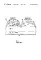
- special arrangementsare made to provide tunnel junction as low resistance contact between the source region and the source contact as that shown in FIG. 1 .
- a P+ region 58is provided to complete an electrical short between the P-base 56 and a N+ source region 66 .
- the electrical shortconsists of three components.
- a first componentis a junction 82 between the P region 58 and the N+ source 66 where a tunnel junction 82 is formed because each of these regions are heavily doped, e.g., each region are doped with 10 19 dopant atoms per cubic centimeter of silicon.
- the tunnel junction 82constitutes a low resistance connection between the N+ source region 66 and the P+ region 58 during normal device operation.
- the second component of the electrical shortis provided at a location E includes a the junction 84 between the P-base 56 and the P+ region 58 .
- the junction 84constitutes a low resistance path between the P-base 56 and the P+ region 58 because the holes can freely pass from the P-base 56 to the P+ region 58 .
- the third component of the electrical short at the location Eincludes the P+ region 58 , in the vicinity of location E, between the tunnel junction 82 and the junction 84 . This is because the region 58 is highly doped and thus constitutes a low resistance path between the junctions 82 and 84 . All these three low resistance paths collectively provide a low resistance path between the P-base 56 and the source region 66 .
- the device structure of providing an electrical short by combining three components of low resistance pathsis very complicate and therefore difficult to control the quality of the electrical paths with predictable resistance. Very accurate control of many parameters during the fabrication process are required in order to assure good quality low resistance electrical paths are achieved for this kind of device structure.
- the device as disclosed by Baliga et al.may appear advantageous in theory but practically, such a device may be too complicate for actual implementation.
- the resistance between the source metal and the N+ sourceis high, especially when the drain to source voltage V DS is small. Such a device may become difficult to switch for a low on-resistance power MOSFET device.
- shortened source regionscan be manufactured on the semiconductor while direct and reliable source contact can also be formed with simplified manufacture processes such that power transistors of increased ruggedness can be manufactured with reliable performance without unduly incurring increased production costs.
- Another object of the present inventionis to provide an improved trenched DMOS structure and fabrication process by employing specially configured trench mask with trenches opened in the body regions for carrying out a source implant over the trench mask to form trench edge source-extension for forming source contact metal thereon whereby a reliable source can be conveniently manufactured without being limited by the narrow width of the source regions.
- Another object of the present inventionis to provide an improved trenched DMOS structure and fabrication process by employing specially configured trench mask for opening trenches in the body regions and for carrying out a source implant over the trench mask to trench edge source-extension for forming source contact metal thereon whereby a reliable source can be conveniently manufactured without increasing any increase in manufacture costs or applying more complicated processing steps.
- Another object of the present inventionis to provide an improved trenched DMOS structure and fabrication process by employing specially configured trench mask for opening trenches in the body regions and for carrying out a source implant over the trench mask to trench edge source-extension for forming source contact metal thereon whereby a reliable source can be conveniently manufactured without requiring a separate source mask to achieve cost savings in manufacturing the DMOS transistors.
- this inventiondiscloses a preferred embodiment which is DMOS transistor on a substrate with specially configured source contacts formed in the trenches in the p-body regions extending over the p-body to touch the source regions.
- This improved DMOS transistor with novel cell structureis manufactured by an improved method to provide better source contacts formed in the trenches.
- the method of manufacturing this improved DMOS transistoris form a DMOS transistor on a substrate with specially configured trench mask to provide trenches filled with polysilicon disposed in a center portion of the DMOS cells such that the DMOS cells which are made with very short source width can be provided with good and reliable source contacts.
- the methodincludes the steps of: (a) forming an epi-layer of a first conductivity type as a drain region on the substrate and then growing an initial oxide layer over the epi-layer; (b) applying an active layer for etching the initial oxide layer to define an active area; (c) performing a blank body implant with impurities of a second conductivity type followed by a body-diffusion process at an elevated temperature thus forming a body layer; (d) applying a trench mask including a plurality of specially configured source contact trenches; (e) performing a source implant with impurities of a first conductivity type followed by a source diffusion at an elevated temperature thus forming a plurality of source regions and trench edge source-extension; (f) etching a plurality of trenches and source contact trenches in the substrate; and (e) removing the trench mask followed by carrying out steps to form a gate and the trenched source contacts in each of the trenches.
- this inventiondiscloses a DMOS transistor cell, supported on a substrate of a first conductivity type.
- the DMOS transistor cellincludes a body region of a second conductivity type disposed in the substrate defining a central portion of the cell.
- This DMOS transistor cellfurther includes a trench gate filled with polysilicon therein surrounding the body region and defining a boundary of the cell.
- This DMOS transistor cellfurther includes a source of the first conductivity type defined by a narrow strip of source region disposed in the body region along an edge thereof adjacent to the trench gate.
- This transistor cellfurther includes a source contact defined by a trench-edge source-extension surrounding the cross-shaped trenches filled with polysilicon disposed in the body region wherein said source-extension extending laterally between the narrow strip of source region and in electric contact thereto for providing area for electrically connecting to a source contact to be formed thereon whereby the source contact can be more conveniently manufactured provided with reliable good contact with the narrow strip of source region.
- FIG. 1is a cross-sectional view of a prior art structure of a trenched semiconductor transistor with a shortened source and a structure to form the three-component source contacts;
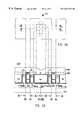
- FIGS. 2A to 2 Care cross-sectional views of a trenched DMOS transistor of the present invention with trenched-source contact specially opened in the body regions;
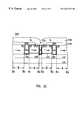
- FIG. 2Dis a top view of the trenched DMOS transistor which is manufactured according the process flow depicted in FIGS. 3A to 3 G below;
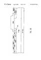
- FIGS. 3A to 3 Gare cross sectional views to show the processing steps for manufacturing a trenched DMOS transistor according to the present invention wherein a novel source contact trenches are opened in the body regions to provide trenched source contact.
- FIGS. 2Ais a top view and FIGS. 2B and 2C are cross sectional views along A-A′ and B-B′ respectively of a DMOS transistor 100 according to the present invention.
- the DMOS transistor 100is formed on a N+ substrate 105 supporting a N epi-layer 110 thereon.
- the N-epi layer 110 together with the substrate 105constitutes a common drain region for the DMOS transistor 100 .
- the DMOS transistor 100includes a plurality of transistor cells 104 each surrounded by gates 125 formed in a trench.
- the DMOS transistor cell 104includes a p-body region 120 disposed above the N-epi layer 110 .
- the DMOS transistor cell 104further includes a source region 115 .
- a novel structural feature included in the DMOS cell 104is a trenched source contact 125 ′ formed in the middle portion of the p-body 120 extending laterally across the p-body thus contacting the source region 115 along the edges of the transistor cell 104 .
- the trenched source contacts 125are formed in a trench filled with polysilicon therein. As shown in these drawings, the source contact trenches are formed to laterally extend across the p-body region to directly touch the n-source regions which are formed with very narrow width. The polysilicon filling the source contact trenches thus provide electrical connections to the source regions near the edges of the transistor cell 104 .
- a layer of metal contact 150is thenformed thereon to provide direct electric connection through opening in a BPSG layer 145 to the source regions 115 through these trenched source contacts 125 ′.
- the DMOS transistor cell 104 as shown in FIGS. 2A to 2 Care manufactured with very narrow source regions 115 .
- the problems of the prior artare resolved. With these trench edge source extension 115 ′, the difficulties caused by the limitations of insufficient areas provided for source contacts as the device patented by Baliga et al., i.e., U.S. Pat. No. 4,567,641, are eliminated.
- the specially configured trench edge source extension 115 ′ formed around the trenches 125 ′provides a further advantage that the cell structure of this novel configuration can be manufactured with almost identical processing steps as that applied in a typical conventional manufacture process.
- the only difference for manufacturing this novel cell structureis to apply a specially configured trench mask. Therefore, there is no increase in production costs, nor does it complicate the manufacture processes as that described below.
- the present inventiondiscloses a DMOS transistor cell 104 supported on a substrate 105 of a first conductivity type.
- the DMOS transistor cellincludes a body region 120 of a second conductivity type disposed in the substrate defining a central portion of the cell.
- This DMOS transistor cellfurther includes a trench gate 125 filled with polysilicon therein surrounding the body region 120 and defining a boundary of the cell.
- This DMOS transistor cell 104further includes a source 115 of the first conductivity type defined by a narrow strip of source region 115 disposed in the body region 120 along an edge thereof adjacent to the trench gate 125 ′.
- This transistor cell 104further includes a source contact 125 ′ defined by a cross-shaped trench filled with polysilicon disposed in the body region 120 surrounded by a trench edge source extension 115 ′ extending laterally between the narrow strip of source region 115 and in electric contact thereto for providing area for electrically connecting to a source contact 150 to be formed thereon whereby the source contact 125 ′ can be more conveniently manufactured provided with reliable good contact with the narrow strip of source region 115 .
- this inventionalso discloses power transistor cell 104 supported on a semiconductor substrate 105 .
- This power transistor cellincludes a body region 120 disposed in the substrate 105 defining a central portion of the cell 104 .
- This power transistor cellfurther includes a trench gate 125 filled with conductive material therein surrounding the body region 120 and defining a boundary of the cell 104 .
- This power transistor cellfurther includes a source region 115 disposed in the body region 120 adjacent to the trench gate 125 ′.
- This power transistor cell 104further includes a source contact 125 ′ defined by a source contact trench filled with a conductive material therein surrounded by a trench edge source extension 115 ′ disposed in the body region 120 and in electrical contact with the source region 115 for providing a more reliable source connection thereto.
- the power transistor cell 104further includes an insulating layer covering the transistor cell 104 wherein a contact window is defined above the source contact trench 125 ′ with contact metal 150 filled therein for contacting the trench edge source extension 115 ′ surrounding the source contact trench 125 ′ and connected to the source region 115 therefrom.
- the source region 115having a width ranging from 0.2 to 0.8 ⁇ m and the source contact trench 125 ′ having a trench width ranging from 0.5 to 2.0 ⁇ m whereby a transistor cell of narrow source is provided with improved ruggedness while maintaining reliable source contact connected by the trench edge source extension 115 ′ disposed around the source contact trench 125 ′ extended thereto.
- FIG. 2Dis a top view of the trenched DMOS transistor cell 104 as described above and which is manufactured according the process flow depicted in FIGS. 3A to 3 G below.
- the DMOS cell 104is supported on a substrate 105 of a first conductivity type, a N-type substrate.
- the DMOS transistor cell 104includes a body region 120 of a second conductivity type, e.g., a p-type body, disposed in the substrate defining a central portion of the cell 104 .
- the DMOS transistor cell 104further includes a trench gate 125 filled with polysilicon therein surrounding the body region 120 and defining a boundary of the cell 104 .
- the DMOS transistor cellfurther includes a source of the first conductivity type, e.g., a N-type source region 115 , defined by a narrow strip of source region 115 disposed in the body region along an edge thereof adjacent to the trench gate 125 .
- the DMOS transistor cell 104further includes a source contact 125 ′ defined by a cross-shaped trench 125 ′ filled with polysilicon disposed in the body region 120 surrounded by a trench edge source extension 115 ′ extending laterally between the narrow strip of source region 115 and in electric contact thereto for providing area for electrically connecting to a metal source contact 150 to be formed thereon whereby the metal source contact 150 can be more conveniently manufactured provided with reliable good contact with the narrow strip of source region 115 .
- the shaded areasare to show that the source region 115 is implanted without requiring a source mask.
- a trench maskis used to carry out the source implant first followed by a diffusion operation. Then the trench mask is utilized to open the trenches for the gate 125 and the cross-shaped source contact trench 125 ′.
- the shaded areas along the trenchesillustrate that there is a narrow strip of N-type region diffused from a N-implant in forming the source region 115 applying the trench mask.
- the processing stepsbegins by first growing a N epitaxial layer 110 with a resistivity ranging from 0.1 to 1.0 ohm-cm on top of a N+ substrate 105 .
- the substratehas a resistivity of 0.001 to 0.007 ohm-cm.
- the thickness and the resistivity of the epitaxial layer 110depend on the device requirements for the on-resistance and breakdown voltage. In a preferred embodiment, the thickness of the epi-layer 110 is about three to twenty microns (3-20 ⁇ m).
- An initial oxidation processis performed to grow an oxide layer 106 ranging from 5,000 to 10,000 ⁇ and active mask is employed to remove the initial oxide layer 106 to define the active regions.
- a blank p-boy implantis carried out with boron ions at 30-100 Kev with an ion beam of 2 ⁇ 10 13 to 2 ⁇ 10 14 /cm 2 flux density to form the p-body region 120 .
- a p-body diffusion processis then carried out at an elevated temperature of 1,000-1,200° C. for ten minutes to three hours to increase the depth of the p-body region 120 to 1.0-2.0 ⁇ .
- An oxide layer 112with a thickness ranging from 1000 to 4000 angstroms, is deposited on the top surface as the trench mask to form the trench gate 125 and the trench source contact 125 ′ as that shown FIGS. 2A to 2 C.
- a N+ implant to form the N+ region 115is carried out.
- the N+ implantationis carried out with an arsenic or phosphorus ion beam at an energy of 40-100 Kev and ion flux density of 5 ⁇ 10 15 to 1 ⁇ 10 16 /cm 2 .
- the N+ source regions 115 and a trench-edge source extension 115 ′ surrounding the trenches opened in the body regionsare driven into desired junction depth ranging from 0.2 to 1.0 ⁇ by a diffusion process at a temperature of 900-1000° C. for 10 minutes to two hours. Therefore, the source regions 115 and the trench-edge source extension 115 ′ are formed without employing a source mask. Cost savings are achieved by the novel fabrication process of this invention when less masks are employed in manufacturing the MOSFET device.
- a trench etch processis performed. It is to be noted that the trench mask 112 is specially configured to provide openings for etching the source-contact trenches 125 ′ to form a plurality of source-contact trenched-connections therein which will be further described below.
- a trench etch processwhich is a dry an-isotropic etch process, is applied to form trenches of 1.0 to 2.0 microns in width and 1.0 to 2.0 micron in depth.
- a sacrification oxidation processis applied which can be either a dry or wet oxidation process conducted at a temperature of 900-1100° C.
- a gate oxide layer 122is then formed by a gate oxidation process which can be a wet or dry oxidation process carried out at a temperature of 800 to 1100° C. to form a layer of thickness in the range of 200 to 1,000 ⁇ .
- a poly deposition processis performed to deposit a poly layer 125 and 125 ′ ranging from 1.5 to 3.0 ⁇ in thickness.
- a planarization etchis performed to form a planar surface by etching a top layer to 0.2-0.5 ⁇ from the deposited poly.
- a POCL 3 doping processis carried out at 950° C. to make the poly layer 125 have a sheet resistance of 20-40 ohm/cm 2 .
- a polysilicon etchis carried out to dry etch the polysilicon layer 125 , including the specially configured source-contact trenched connection 125 ′, till the top surface is removed with the end-point detection to terminate the etch process when the polysilicon layer above the trench is removed.
- a BPSG or PSGis deposited to form a layer 145 of approximately 5000-15,000 ⁇ in thickness.
- a BPSG flow or BSG densification processis performed at 900-950° C. for thirty minutes to one hour.
- a contact mask(not shown) is applied to perform a dry etch process to define the contacts windows in order to be ready for making source and gate contacts.
- a blank boron implant with an ion beam of 20-50 Kev and ion flux of 10 15 to 1 ⁇ 10 16 /cm 2is carried out to form the p+ regions 130 for providing a low-resistance body contact of the DMOS cell.
- a metal deposition processis carried out to form an overlaying metal layer.
- the final DMOS transistor 100is completed by applying a metal mask to pattern the source contact 150 , the gate contact, the field plate and the channel stop (CS).
- a source-contact trenched connections 125 ′are formed in each cell as that shown FIGS. 2A to 2 C wherein each of these DMOS cells can be made with source regions having very short width while good and reliable contacts are provided with specially configured source contact trenched connections 125 ′.
- this inventiondiscloses a method for fabricating a DMOS transistor 100 on a substrate 105 with specially configured trench mask to provide trenches filled with conductive polysilicon disposed in a center portion of the DMOS cells surrounded by a trench-edge source extension 115 ′ such that the DMOS cells which are made with very short source width can be provided with good and reliable source contacts.
- the methodincludes the steps of: (a) forming an epi-layer 110 of a first conductivity type as a drain region on the substrate and then growing an initial oxide layer over the epi-layer; (b) applying an active layer for etching the initial oxide layer to define an active area; (c) performing a blank body implant with impurities of a second conductivity type followed by a body-diffusion process at an elevated temperature thus forming a body layer 120 ; (d) applying a trench mask including a specially configured source contact trench to first carrying out a source implant followed by a source diffusion to form a source region and a trench-edge source extension without requiring a source mask; and (e) applying the trench mask or etching a plurality of gate trenches and source contact trenches in the substrate wherein the source contact trenches extending laterally in the body layer.
- the method for fabricating the transistorfurther includes a step of: (f) removing the trench mask followed by carrying out steps to form a gate in each of the trenches and a source contact in each of the source contact trenches.
- the step (e) of applying a trench mask for etching a plurality of gate trenches and source contact trenches in the substratefurther includes a step of applying the trench mask to etch a plurality of gates trenches and source contact trenches leaving a narrow strip of source implant region along the trenches.
- the step (f) of carrying out steps to form a gate in each of the trenches and a source contact in each of the source contact trenchesis a step of depositing a polysilicon in each of the gate trenches and the source contact trenches.
- the methodfurther includes a step (g) forming an insulation layer covering the transistor followed by applying a contact mask for opening a source contact window above the source contact for forming a source contact therein by filling a conductive material in the source contact window thus contacting the source regions through an interconnection of the source contact in the source contact trenches laterally extending to the source regions.
- an improved trenched DMOS transistoris disclosed by simply applying a specially configured trench mask provided with openings above the body regions to form specially shaped trenches and source contacts with a trench edge source extension whereby reliable source contacts are conveniently formed.
- a specially configured trench maskprovided with openings above the body regions to form specially shaped trenches and source contacts with a trench edge source extension whereby reliable source contacts are conveniently formed.
Landscapes
- Insulated Gate Type Field-Effect Transistor (AREA)
- Metal-Oxide And Bipolar Metal-Oxide Semiconductor Integrated Circuits (AREA)
Abstract
Description
Claims (10)
Priority Applications (1)
| Application Number | Priority Date | Filing Date | Title |
|---|---|---|---|
| US08/853,150US6281547B1 (en) | 1997-05-08 | 1997-05-08 | Power transistor cells provided with reliable trenched source contacts connected to narrower source manufactured without a source mask |
Applications Claiming Priority (1)
| Application Number | Priority Date | Filing Date | Title |
|---|---|---|---|
| US08/853,150US6281547B1 (en) | 1997-05-08 | 1997-05-08 | Power transistor cells provided with reliable trenched source contacts connected to narrower source manufactured without a source mask |
Publications (1)
| Publication Number | Publication Date |
|---|---|
| US6281547B1true US6281547B1 (en) | 2001-08-28 |
Family
ID=25315209
Family Applications (1)
| Application Number | Title | Priority Date | Filing Date |
|---|---|---|---|
| US08/853,150Expired - LifetimeUS6281547B1 (en) | 1997-05-08 | 1997-05-08 | Power transistor cells provided with reliable trenched source contacts connected to narrower source manufactured without a source mask |
Country Status (1)
| Country | Link |
|---|---|
| US (1) | US6281547B1 (en) |
Cited By (56)
| Publication number | Priority date | Publication date | Assignee | Title |
|---|---|---|---|---|
| US6445036B1 (en)* | 1999-08-23 | 2002-09-03 | Nec Corporation | Semiconductor device having trench-structured rectangular unit cells |
| US6476442B1 (en)* | 1996-05-15 | 2002-11-05 | Siliconix Incorporated | Pseudo-Schottky diode |
| US6525375B1 (en)* | 1999-10-19 | 2003-02-25 | Denso Corporation | Semiconductor device having trench filled up with gate electrode |
| US6597043B1 (en)* | 2001-11-13 | 2003-07-22 | National Semiconductor Corporation | Narrow high performance MOSFET device design |
| US20030197239A1 (en)* | 2002-04-18 | 2003-10-23 | Oleg Siniaguine | Clock distribution networks and conductive lines in semiconductor integrated circuits |
| WO2003085722A3 (en)* | 2002-03-29 | 2003-11-27 | Fairchild Semiconductor | Field effect transistor having a lateral depletion structure |
| US6670673B2 (en) | 2001-04-18 | 2003-12-30 | Denso Corporation | Semiconductor device and method for manufacturing semiconductor device |
| US6710403B2 (en)* | 2002-07-30 | 2004-03-23 | Fairchild Semiconductor Corporation | Dual trench power MOSFET |
| US20040132252A1 (en)* | 2001-01-30 | 2004-07-08 | Merchant Bruce D. | Method of forming a field effect transistor having a lateral depletion structure |
| US20040145015A1 (en)* | 1997-11-14 | 2004-07-29 | Fairchild Semiconductor Corporation | Field effect transistor and method of its manufacture |
| US6777756B2 (en)* | 2001-03-26 | 2004-08-17 | Kabushiki Kaisha Toshiba | Semiconductor device |
| US20060011990A1 (en)* | 2004-07-15 | 2006-01-19 | International Business Machines Corporation | Method for fabricating strained semiconductor structures and strained semiconductor structures formed thereby |
| US6991977B2 (en) | 2001-10-17 | 2006-01-31 | Fairchild Semiconductor Corporation | Method for forming a semiconductor structure with improved smaller forward voltage loss and higher blocking capability |
| US7265415B2 (en) | 2004-10-08 | 2007-09-04 | Fairchild Semiconductor Corporation | MOS-gated transistor with reduced miller capacitance |
| US7265416B2 (en) | 2002-02-23 | 2007-09-04 | Fairchild Korea Semiconductor Ltd. | High breakdown voltage low on-resistance lateral DMOS transistor |
| US7291894B2 (en) | 2002-07-18 | 2007-11-06 | Fairchild Semiconductor Corporation | Vertical charge control semiconductor device with low output capacitance |
| US7301203B2 (en) | 2003-11-28 | 2007-11-27 | Fairchild Korea Semiconductor Ltd. | Superjunction semiconductor device |
| US7319256B1 (en) | 2006-06-19 | 2008-01-15 | Fairchild Semiconductor Corporation | Shielded gate trench FET with the shield and gate electrodes being connected together |
| US7345342B2 (en) | 2001-01-30 | 2008-03-18 | Fairchild Semiconductor Corporation | Power semiconductor devices and methods of manufacture |
| US7352036B2 (en) | 2004-08-03 | 2008-04-01 | Fairchild Semiconductor Corporation | Semiconductor power device having a top-side drain using a sinker trench |
| CN100382333C (en)* | 2004-09-09 | 2008-04-16 | 敦南科技股份有限公司 | Power semiconductor device with improved strength |
| US7368777B2 (en) | 2003-12-30 | 2008-05-06 | Fairchild Semiconductor Corporation | Accumulation device with charge balance structure and method of forming the same |
| US7385248B2 (en) | 2005-08-09 | 2008-06-10 | Fairchild Semiconductor Corporation | Shielded gate field effect transistor with improved inter-poly dielectric |
| US7429523B2 (en) | 2001-10-17 | 2008-09-30 | Fairchild Semiconductor Corporation | Method of forming schottky diode with charge balance structure |
| US7504306B2 (en) | 2005-04-06 | 2009-03-17 | Fairchild Semiconductor Corporation | Method of forming trench gate field effect transistor with recessed mesas |
| US20090185404A1 (en)* | 2007-09-26 | 2009-07-23 | Lakota Technologies, Inc. | Regenerative Building Block and Diode Bridge Rectifier and Methods |
| US7576388B1 (en) | 2002-10-03 | 2009-08-18 | Fairchild Semiconductor Corporation | Trench-gate LDMOS structures |
| US7582519B2 (en) | 2002-11-05 | 2009-09-01 | Fairchild Semiconductor Corporation | Method of forming a trench structure having one or more diodes embedded therein adjacent a PN junction |
| US20090267111A1 (en)* | 2007-09-26 | 2009-10-29 | Lakota Technologies, Inc. | MOSFET with Integrated Field Effect Rectifier |
| WO2009134812A1 (en) | 2008-04-28 | 2009-11-05 | Lakota Technologies, Inc. | Mosfet with integrated field effect rectifier |
| US7625793B2 (en) | 1999-12-20 | 2009-12-01 | Fairchild Semiconductor Corporation | Power MOS device with improved gate charge performance |
| US7638841B2 (en) | 2003-05-20 | 2009-12-29 | Fairchild Semiconductor Corporation | Power semiconductor devices and methods of manufacture |
| KR100952577B1 (en) | 2003-01-14 | 2010-04-12 | 매그나칩 반도체 유한회사 | ISD protective circuit with cross finger structure |
| US7713822B2 (en) | 2006-03-24 | 2010-05-11 | Fairchild Semiconductor Corporation | Method of forming high density trench FET with integrated Schottky diode |
| US7745289B2 (en) | 2000-08-16 | 2010-06-29 | Fairchild Semiconductor Corporation | Method of forming a FET having ultra-low on-resistance and low gate charge |
| US7772668B2 (en) | 2007-12-26 | 2010-08-10 | Fairchild Semiconductor Corporation | Shielded gate trench FET with multiple channels |
| US20100271851A1 (en)* | 2007-09-26 | 2010-10-28 | Lakota Technologies Inc. | Self-bootstrapping field effect diode structures and methods |
| US20100308402A1 (en)* | 2009-06-08 | 2010-12-09 | Suku Kim | 3d channel architecture for semiconductor devices |
| US20110051305A1 (en)* | 2007-09-26 | 2011-03-03 | Lakota Technologies Inc. | Series Current Limiter Device |
| US20110254084A1 (en)* | 2010-03-02 | 2011-10-20 | Vishay-Siliconix | Structures and methods of fabricating dual gate devices |
| US8319290B2 (en) | 2010-06-18 | 2012-11-27 | Fairchild Semiconductor Corporation | Trench MOS barrier schottky rectifier with a planar surface using CMP techniques |
| CN103219241A (en)* | 2012-01-19 | 2013-07-24 | 立新半导体有限公司 | Method of preparing groove discrete semiconductor device |
| US8673700B2 (en) | 2011-04-27 | 2014-03-18 | Fairchild Semiconductor Corporation | Superjunction structures for power devices and methods of manufacture |
| US8772868B2 (en) | 2011-04-27 | 2014-07-08 | Fairchild Semiconductor Corporation | Superjunction structures for power devices and methods of manufacture |
| US8786010B2 (en) | 2011-04-27 | 2014-07-22 | Fairchild Semiconductor Corporation | Superjunction structures for power devices and methods of manufacture |
| US8836028B2 (en) | 2011-04-27 | 2014-09-16 | Fairchild Semiconductor Corporation | Superjunction structures for power devices and methods of manufacture |
| US8872278B2 (en) | 2011-10-25 | 2014-10-28 | Fairchild Semiconductor Corporation | Integrated gate runner and field implant termination for trench devices |
| US8928077B2 (en) | 2007-09-21 | 2015-01-06 | Fairchild Semiconductor Corporation | Superjunction structures for power devices |
| US20160233308A1 (en)* | 2013-08-07 | 2016-08-11 | Infineon Technologies Ag | Semiconductor device and method for producing same |
| US9419129B2 (en) | 2009-10-21 | 2016-08-16 | Vishay-Siliconix | Split gate semiconductor device with curved gate oxide profile |
| US9425305B2 (en) | 2009-10-20 | 2016-08-23 | Vishay-Siliconix | Structures of and methods of fabricating split gate MIS devices |
| US9431481B2 (en) | 2008-09-19 | 2016-08-30 | Fairchild Semiconductor Corporation | Superjunction structures for power devices and methods of manufacture |
| US10234486B2 (en) | 2014-08-19 | 2019-03-19 | Vishay/Siliconix | Vertical sense devices in vertical trench MOSFET |
| US11114559B2 (en) | 2011-05-18 | 2021-09-07 | Vishay-Siliconix, LLC | Semiconductor device having reduced gate charges and superior figure of merit |
| US11217541B2 (en) | 2019-05-08 | 2022-01-04 | Vishay-Siliconix, LLC | Transistors with electrically active chip seal ring and methods of manufacture |
| US11218144B2 (en) | 2019-09-12 | 2022-01-04 | Vishay-Siliconix, LLC | Semiconductor device with multiple independent gates |
Citations (5)
| Publication number | Priority date | Publication date | Assignee | Title |
|---|---|---|---|---|
| US5173435A (en)* | 1987-11-11 | 1992-12-22 | Mitsubishi Denki Kabushiki Kaisha | Insulated gate bipolar transistor |
| US5414290A (en)* | 1993-05-07 | 1995-05-09 | Abb Management Ag | IGBT with self-aligning cathode pattern and method for producing it |
| US5721148A (en)* | 1995-12-07 | 1998-02-24 | Fuji Electric Co. | Method for manufacturing MOS type semiconductor device |
| US5831288A (en)* | 1996-06-06 | 1998-11-03 | Cree Research, Inc. | Silicon carbide metal-insulator semiconductor field effect transistor |
| US5895951A (en)* | 1996-04-05 | 1999-04-20 | Megamos Corporation | MOSFET structure and fabrication process implemented by forming deep and narrow doping regions through doping trenches |
- 1997
- 1997-05-08USUS08/853,150patent/US6281547B1/ennot_activeExpired - Lifetime
Patent Citations (5)
| Publication number | Priority date | Publication date | Assignee | Title |
|---|---|---|---|---|
| US5173435A (en)* | 1987-11-11 | 1992-12-22 | Mitsubishi Denki Kabushiki Kaisha | Insulated gate bipolar transistor |
| US5414290A (en)* | 1993-05-07 | 1995-05-09 | Abb Management Ag | IGBT with self-aligning cathode pattern and method for producing it |
| US5721148A (en)* | 1995-12-07 | 1998-02-24 | Fuji Electric Co. | Method for manufacturing MOS type semiconductor device |
| US5895951A (en)* | 1996-04-05 | 1999-04-20 | Megamos Corporation | MOSFET structure and fabrication process implemented by forming deep and narrow doping regions through doping trenches |
| US5831288A (en)* | 1996-06-06 | 1998-11-03 | Cree Research, Inc. | Silicon carbide metal-insulator semiconductor field effect transistor |
Cited By (126)
| Publication number | Priority date | Publication date | Assignee | Title |
|---|---|---|---|---|
| US6476442B1 (en)* | 1996-05-15 | 2002-11-05 | Siliconix Incorporated | Pseudo-Schottky diode |
| US20100264487A1 (en)* | 1997-11-14 | 2010-10-21 | Brian Sze-Ki Mo | Method of Manufacturing a Trench Transistor Having a Heavy Body Region |
| US20040145015A1 (en)* | 1997-11-14 | 2004-07-29 | Fairchild Semiconductor Corporation | Field effect transistor and method of its manufacture |
| US7696571B2 (en) | 1997-11-14 | 2010-04-13 | Fairchild Semiconductor Corporation | Method of manufacturing a trench transistor having a heavy body region |
| US20090134458A1 (en)* | 1997-11-14 | 2009-05-28 | Brian Sze-Ki Mo | Method of Manufacturing a Trench Transistor Having a Heavy Body Region |
| US20100112767A1 (en)* | 1997-11-14 | 2010-05-06 | Brian Sze-Ki Mo | Method of Manufacturing a Trench Transistor Having a Heavy Body Region |
| US7511339B2 (en) | 1997-11-14 | 2009-03-31 | Fairchild Semiconductor Corporation | Field effect transistor and method of its manufacture |
| US7736978B2 (en) | 1997-11-14 | 2010-06-15 | Fairchild Semiconductor Corporation | Method of manufacturing a trench transistor having a heavy body region |
| US8044463B2 (en) | 1997-11-14 | 2011-10-25 | Fairchild Semiconductor Corporation | Method of manufacturing a trench transistor having a heavy body region |
| US8476133B2 (en) | 1997-11-14 | 2013-07-02 | Fairchild Semiconductor Corporation | Method of manufacture and structure for a trench transistor having a heavy body region |
| US20070042551A1 (en)* | 1997-11-14 | 2007-02-22 | Mo Brian S | Method of manufacturing a trench transistor having a heavy body region |
| US6445036B1 (en)* | 1999-08-23 | 2002-09-03 | Nec Corporation | Semiconductor device having trench-structured rectangular unit cells |
| US6525375B1 (en)* | 1999-10-19 | 2003-02-25 | Denso Corporation | Semiconductor device having trench filled up with gate electrode |
| US6696323B2 (en) | 1999-10-19 | 2004-02-24 | Denso Corporation | Method of manufacturing semiconductor device having trench filled up with gate electrode |
| US7625793B2 (en) | 1999-12-20 | 2009-12-01 | Fairchild Semiconductor Corporation | Power MOS device with improved gate charge performance |
| US8710584B2 (en) | 2000-08-16 | 2014-04-29 | Fairchild Semiconductor Corporation | FET device having ultra-low on-resistance and low gate charge |
| US7745289B2 (en) | 2000-08-16 | 2010-06-29 | Fairchild Semiconductor Corporation | Method of forming a FET having ultra-low on-resistance and low gate charge |
| US8101484B2 (en) | 2000-08-16 | 2012-01-24 | Fairchild Semiconductor Corporation | Method of forming a FET having ultra-low on-resistance and low gate charge |
| US20040132252A1 (en)* | 2001-01-30 | 2004-07-08 | Merchant Bruce D. | Method of forming a field effect transistor having a lateral depletion structure |
| US9368587B2 (en) | 2001-01-30 | 2016-06-14 | Fairchild Semiconductor Corporation | Accumulation-mode field effect transistor with improved current capability |
| US6818513B2 (en) | 2001-01-30 | 2004-11-16 | Fairchild Semiconductor Corporation | Method of forming a field effect transistor having a lateral depletion structure |
| US7345342B2 (en) | 2001-01-30 | 2008-03-18 | Fairchild Semiconductor Corporation | Power semiconductor devices and methods of manufacture |
| US8829641B2 (en) | 2001-01-30 | 2014-09-09 | Fairchild Semiconductor Corporation | Method of forming a dual-trench field effect transistor |
| US6777756B2 (en)* | 2001-03-26 | 2004-08-17 | Kabushiki Kaisha Toshiba | Semiconductor device |
| US20040089896A1 (en)* | 2001-04-18 | 2004-05-13 | Jun Sakakibara | Semiconductor device having high breakdown voltage without increased on resistance |
| US6670673B2 (en) | 2001-04-18 | 2003-12-30 | Denso Corporation | Semiconductor device and method for manufacturing semiconductor device |
| US6867456B2 (en) | 2001-04-18 | 2005-03-15 | Denso Corporation | Semiconductor device having high breakdown voltage without increased on resistance |
| US7429523B2 (en) | 2001-10-17 | 2008-09-30 | Fairchild Semiconductor Corporation | Method of forming schottky diode with charge balance structure |
| US6991977B2 (en) | 2001-10-17 | 2006-01-31 | Fairchild Semiconductor Corporation | Method for forming a semiconductor structure with improved smaller forward voltage loss and higher blocking capability |
| US6597043B1 (en)* | 2001-11-13 | 2003-07-22 | National Semiconductor Corporation | Narrow high performance MOSFET device design |
| US6709936B1 (en) | 2001-11-13 | 2004-03-23 | National Semiconductor Corporation | Narrow high performance MOSFET device design |
| US7265416B2 (en) | 2002-02-23 | 2007-09-04 | Fairchild Korea Semiconductor Ltd. | High breakdown voltage low on-resistance lateral DMOS transistor |
| US7605040B2 (en) | 2002-02-23 | 2009-10-20 | Fairchild Korea Semiconductor Ltd. | Method of forming high breakdown voltage low on-resistance lateral DMOS transistor |
| WO2003085722A3 (en)* | 2002-03-29 | 2003-11-27 | Fairchild Semiconductor | Field effect transistor having a lateral depletion structure |
| US7173327B2 (en) | 2002-04-18 | 2007-02-06 | Tru-Si Technologies, Inc. | Clock distribution networks and conductive lines in semiconductor integrated circuits |
| US20070069377A1 (en)* | 2002-04-18 | 2007-03-29 | Oleg Siniaguine | Clock distribution networks and conductive lines in semiconductor integrated circuits |
| US20050051887A1 (en)* | 2002-04-18 | 2005-03-10 | Oleg Siniaguine | Clock distribution networks and conductive lines in semiconductor integrated circuits |
| US20030197239A1 (en)* | 2002-04-18 | 2003-10-23 | Oleg Siniaguine | Clock distribution networks and conductive lines in semiconductor integrated circuits |
| US20050207238A1 (en)* | 2002-04-18 | 2005-09-22 | Oleg Siniaguine | Clock distribution networks and conductive lines in semiconductor integrated circuits |
| US7977744B2 (en) | 2002-07-18 | 2011-07-12 | Fairchild Semiconductor Corporation | Field effect transistor with trench filled with insulating material and strips of semi-insulating material along trench sidewalls |
| US7291894B2 (en) | 2002-07-18 | 2007-11-06 | Fairchild Semiconductor Corporation | Vertical charge control semiconductor device with low output capacitance |
| US6710403B2 (en)* | 2002-07-30 | 2004-03-23 | Fairchild Semiconductor Corporation | Dual trench power MOSFET |
| US8198677B2 (en) | 2002-10-03 | 2012-06-12 | Fairchild Semiconductor Corporation | Trench-gate LDMOS structures |
| US7576388B1 (en) | 2002-10-03 | 2009-08-18 | Fairchild Semiconductor Corporation | Trench-gate LDMOS structures |
| US7582519B2 (en) | 2002-11-05 | 2009-09-01 | Fairchild Semiconductor Corporation | Method of forming a trench structure having one or more diodes embedded therein adjacent a PN junction |
| KR100952577B1 (en) | 2003-01-14 | 2010-04-12 | 매그나칩 반도체 유한회사 | ISD protective circuit with cross finger structure |
| US7982265B2 (en) | 2003-05-20 | 2011-07-19 | Fairchild Semiconductor Corporation | Trenched shield gate power semiconductor devices and methods of manufacture |
| US8889511B2 (en) | 2003-05-20 | 2014-11-18 | Fairchild Semiconductor Corporation | Methods of manufacturing power semiconductor devices with trenched shielded split gate transistor |
| US7638841B2 (en) | 2003-05-20 | 2009-12-29 | Fairchild Semiconductor Corporation | Power semiconductor devices and methods of manufacture |
| US7652326B2 (en) | 2003-05-20 | 2010-01-26 | Fairchild Semiconductor Corporation | Power semiconductor devices and methods of manufacture |
| US8143123B2 (en) | 2003-05-20 | 2012-03-27 | Fairchild Semiconductor Corporation | Methods of forming inter-poly dielectric (IPD) layers in power semiconductor devices |
| US8936985B2 (en) | 2003-05-20 | 2015-01-20 | Fairchild Semiconductor Corporation | Methods related to power semiconductor devices with thick bottom oxide layers |
| US8350317B2 (en) | 2003-05-20 | 2013-01-08 | Fairchild Semiconductor Corporation | Power semiconductor devices and methods of manufacture |
| US8013387B2 (en) | 2003-05-20 | 2011-09-06 | Fairchild Semiconductor Corporation | Power semiconductor devices with shield and gate contacts and methods of manufacture |
| US8129245B2 (en) | 2003-05-20 | 2012-03-06 | Fairchild Semiconductor Corporation | Methods of manufacturing power semiconductor devices with shield and gate contacts |
| US8013391B2 (en) | 2003-05-20 | 2011-09-06 | Fairchild Semiconductor Corporation | Power semiconductor devices with trenched shielded split gate transistor and methods of manufacture |
| US7855415B2 (en) | 2003-05-20 | 2010-12-21 | Fairchild Semiconductor Corporation | Power semiconductor devices having termination structures and methods of manufacture |
| US8143124B2 (en) | 2003-05-20 | 2012-03-27 | Fairchild Semiconductor Corporation | Methods of making power semiconductor devices with thick bottom oxide layer |
| US8786045B2 (en) | 2003-05-20 | 2014-07-22 | Fairchild Semiconductor Corporation | Power semiconductor devices having termination structures |
| US7655981B2 (en) | 2003-11-28 | 2010-02-02 | Fairchild Korea Semiconductor Ltd. | Superjunction semiconductor device |
| US7301203B2 (en) | 2003-11-28 | 2007-11-27 | Fairchild Korea Semiconductor Ltd. | Superjunction semiconductor device |
| US7368777B2 (en) | 2003-12-30 | 2008-05-06 | Fairchild Semiconductor Corporation | Accumulation device with charge balance structure and method of forming the same |
| US7936008B2 (en) | 2003-12-30 | 2011-05-03 | Fairchild Semiconductor Corporation | Structure and method for forming accumulation-mode field effect transistor with improved current capability |
| US8518777B2 (en) | 2003-12-30 | 2013-08-27 | Fairchild Semiconductor Corporation | Method for forming accumulation-mode field effect transistor with improved current capability |
| US20060011990A1 (en)* | 2004-07-15 | 2006-01-19 | International Business Machines Corporation | Method for fabricating strained semiconductor structures and strained semiconductor structures formed thereby |
| US7102201B2 (en)* | 2004-07-15 | 2006-09-05 | International Business Machines Corporation | Strained semiconductor device structures |
| US7732876B2 (en) | 2004-08-03 | 2010-06-08 | Fairchild Semiconductor Corporation | Power transistor with trench sinker for contacting the backside |
| US7352036B2 (en) | 2004-08-03 | 2008-04-01 | Fairchild Semiconductor Corporation | Semiconductor power device having a top-side drain using a sinker trench |
| US8148233B2 (en) | 2004-08-03 | 2012-04-03 | Fairchild Semiconductor Corporation | Semiconductor power device having a top-side drain using a sinker trench |
| US8026558B2 (en) | 2004-08-03 | 2011-09-27 | Fairchild Semiconductor Corporation | Semiconductor power device having a top-side drain using a sinker trench |
| CN100382333C (en)* | 2004-09-09 | 2008-04-16 | 敦南科技股份有限公司 | Power semiconductor device with improved strength |
| US7534683B2 (en) | 2004-10-08 | 2009-05-19 | Fairchild Semiconductor Corporation | Method of making a MOS-gated transistor with reduced miller capacitance |
| US7265415B2 (en) | 2004-10-08 | 2007-09-04 | Fairchild Semiconductor Corporation | MOS-gated transistor with reduced miller capacitance |
| US7504306B2 (en) | 2005-04-06 | 2009-03-17 | Fairchild Semiconductor Corporation | Method of forming trench gate field effect transistor with recessed mesas |
| US8680611B2 (en) | 2005-04-06 | 2014-03-25 | Fairchild Semiconductor Corporation | Field effect transistor and schottky diode structures |
| US8084327B2 (en) | 2005-04-06 | 2011-12-27 | Fairchild Semiconductor Corporation | Method for forming trench gate field effect transistor with recessed mesas using spacers |
| US7598144B2 (en) | 2005-08-09 | 2009-10-06 | Fairchild Semiconductor Corporation | Method for forming inter-poly dielectric in shielded gate field effect transistor |
| US7385248B2 (en) | 2005-08-09 | 2008-06-10 | Fairchild Semiconductor Corporation | Shielded gate field effect transistor with improved inter-poly dielectric |
| US7713822B2 (en) | 2006-03-24 | 2010-05-11 | Fairchild Semiconductor Corporation | Method of forming high density trench FET with integrated Schottky diode |
| US7319256B1 (en) | 2006-06-19 | 2008-01-15 | Fairchild Semiconductor Corporation | Shielded gate trench FET with the shield and gate electrodes being connected together |
| US7859047B2 (en) | 2006-06-19 | 2010-12-28 | Fairchild Semiconductor Corporation | Shielded gate trench FET with the shield and gate electrodes connected together in non-active region |
| US7473603B2 (en) | 2006-06-19 | 2009-01-06 | Fairchild Semiconductor Corporation | Method for forming a shielded gate trench FET with the shield and gate electrodes being connected together |
| US8928077B2 (en) | 2007-09-21 | 2015-01-06 | Fairchild Semiconductor Corporation | Superjunction structures for power devices |
| US9595596B2 (en) | 2007-09-21 | 2017-03-14 | Fairchild Semiconductor Corporation | Superjunction structures for power devices |
| US20100271851A1 (en)* | 2007-09-26 | 2010-10-28 | Lakota Technologies Inc. | Self-bootstrapping field effect diode structures and methods |
| US20090185404A1 (en)* | 2007-09-26 | 2009-07-23 | Lakota Technologies, Inc. | Regenerative Building Block and Diode Bridge Rectifier and Methods |
| US8421118B2 (en) | 2007-09-26 | 2013-04-16 | Stmicroelectronics N.V. | Regenerative building block and diode bridge rectifier and methods |
| US20090267111A1 (en)* | 2007-09-26 | 2009-10-29 | Lakota Technologies, Inc. | MOSFET with Integrated Field Effect Rectifier |
| US9048308B2 (en) | 2007-09-26 | 2015-06-02 | Stmicroelectronics International N.V. | Regenerative building block and diode bridge rectifier and methods |
| US9029921B2 (en) | 2007-09-26 | 2015-05-12 | Stmicroelectronics International N.V. | Self-bootstrapping field effect diode structures and methods |
| US8598620B2 (en) | 2007-09-26 | 2013-12-03 | Stmicroelectronics N.V. | MOSFET with integrated field effect rectifier |
| US8633521B2 (en) | 2007-09-26 | 2014-01-21 | Stmicroelectronics N.V. | Self-bootstrapping field effect diode structures and methods |
| US8643055B2 (en) | 2007-09-26 | 2014-02-04 | Stmicroelectronics N.V. | Series current limiter device |
| US9012954B2 (en) | 2007-09-26 | 2015-04-21 | STMicroelectronics International B.V. | Adjustable field effect rectifier |
| US20110051305A1 (en)* | 2007-09-26 | 2011-03-03 | Lakota Technologies Inc. | Series Current Limiter Device |
| US20100258866A1 (en)* | 2007-12-26 | 2010-10-14 | James Pan | Method for Forming Shielded Gate Trench FET with Multiple Channels |
| US9224853B2 (en) | 2007-12-26 | 2015-12-29 | Fairchild Semiconductor Corporation | Shielded gate trench FET with multiple channels |
| US7772668B2 (en) | 2007-12-26 | 2010-08-10 | Fairchild Semiconductor Corporation | Shielded gate trench FET with multiple channels |
| EP2274770A4 (en)* | 2008-04-28 | 2012-12-26 | St Microelectronics Nv | INTEGRATED FIELD EFFECT RECTIFIER MOSFET |
| WO2009134812A1 (en) | 2008-04-28 | 2009-11-05 | Lakota Technologies, Inc. | Mosfet with integrated field effect rectifier |
| US9431481B2 (en) | 2008-09-19 | 2016-08-30 | Fairchild Semiconductor Corporation | Superjunction structures for power devices and methods of manufacture |
| US20100308402A1 (en)* | 2009-06-08 | 2010-12-09 | Suku Kim | 3d channel architecture for semiconductor devices |
| US8072027B2 (en) | 2009-06-08 | 2011-12-06 | Fairchild Semiconductor Corporation | 3D channel architecture for semiconductor devices |
| US9425305B2 (en) | 2009-10-20 | 2016-08-23 | Vishay-Siliconix | Structures of and methods of fabricating split gate MIS devices |
| US9893168B2 (en) | 2009-10-21 | 2018-02-13 | Vishay-Siliconix | Split gate semiconductor device with curved gate oxide profile |
| US9419129B2 (en) | 2009-10-21 | 2016-08-16 | Vishay-Siliconix | Split gate semiconductor device with curved gate oxide profile |
| US9577089B2 (en)* | 2010-03-02 | 2017-02-21 | Vishay-Siliconix | Structures and methods of fabricating dual gate devices |
| US20110254084A1 (en)* | 2010-03-02 | 2011-10-20 | Vishay-Siliconix | Structures and methods of fabricating dual gate devices |
| US10453953B2 (en)* | 2010-03-02 | 2019-10-22 | Vishay-Siliconix | Structures and methods of fabricating dual gate devices |
| US20170104096A1 (en)* | 2010-03-02 | 2017-04-13 | Vishay-Siliconix | Structures and methods of fabricating dual gate devices |
| US8319290B2 (en) | 2010-06-18 | 2012-11-27 | Fairchild Semiconductor Corporation | Trench MOS barrier schottky rectifier with a planar surface using CMP techniques |
| US8432000B2 (en) | 2010-06-18 | 2013-04-30 | Fairchild Semiconductor Corporation | Trench MOS barrier schottky rectifier with a planar surface using CMP techniques |
| US8772868B2 (en) | 2011-04-27 | 2014-07-08 | Fairchild Semiconductor Corporation | Superjunction structures for power devices and methods of manufacture |
| US8673700B2 (en) | 2011-04-27 | 2014-03-18 | Fairchild Semiconductor Corporation | Superjunction structures for power devices and methods of manufacture |
| US8786010B2 (en) | 2011-04-27 | 2014-07-22 | Fairchild Semiconductor Corporation | Superjunction structures for power devices and methods of manufacture |
| US8836028B2 (en) | 2011-04-27 | 2014-09-16 | Fairchild Semiconductor Corporation | Superjunction structures for power devices and methods of manufacture |
| US11114559B2 (en) | 2011-05-18 | 2021-09-07 | Vishay-Siliconix, LLC | Semiconductor device having reduced gate charges and superior figure of merit |
| US8872278B2 (en) | 2011-10-25 | 2014-10-28 | Fairchild Semiconductor Corporation | Integrated gate runner and field implant termination for trench devices |
| CN103219241A (en)* | 2012-01-19 | 2013-07-24 | 立新半导体有限公司 | Method of preparing groove discrete semiconductor device |
| US20160233308A1 (en)* | 2013-08-07 | 2016-08-11 | Infineon Technologies Ag | Semiconductor device and method for producing same |
| US9917160B2 (en)* | 2013-08-07 | 2018-03-13 | Infineon Technologies Ag | Semiconductor device having a polycrystalline silicon IGFET |
| US10444262B2 (en) | 2014-08-19 | 2019-10-15 | Vishay-Siliconix | Vertical sense devices in vertical trench MOSFET |
| US10234486B2 (en) | 2014-08-19 | 2019-03-19 | Vishay/Siliconix | Vertical sense devices in vertical trench MOSFET |
| US10527654B2 (en) | 2014-08-19 | 2020-01-07 | Vishay SIliconix, LLC | Vertical sense devices in vertical trench MOSFET |
| US11217541B2 (en) | 2019-05-08 | 2022-01-04 | Vishay-Siliconix, LLC | Transistors with electrically active chip seal ring and methods of manufacture |
| US11218144B2 (en) | 2019-09-12 | 2022-01-04 | Vishay-Siliconix, LLC | Semiconductor device with multiple independent gates |
Similar Documents
| Publication | Publication Date | Title |
|---|---|---|
| US6281547B1 (en) | Power transistor cells provided with reliable trenched source contacts connected to narrower source manufactured without a source mask | |
| US5877528A (en) | Structure to provide effective channel-stop in termination areas for trenched power transistors | |
| US10608092B2 (en) | Semiconductor power devices manufactured with self-aligned processes and more reliable electrical contacts | |
| US5895951A (en) | MOSFET structure and fabrication process implemented by forming deep and narrow doping regions through doping trenches | |
| US5763915A (en) | DMOS transistors having trenched gate oxide | |
| US6872611B2 (en) | Method of manufacturing transistor | |
| US6534367B2 (en) | Trench-gate semiconductor devices and their manufacture | |
| US6498071B2 (en) | Manufacture of trench-gate semiconductor devices | |
| JP2662217B2 (en) | Vertical gate semiconductor device and method of manufacturing the same | |
| US6586800B2 (en) | Trench-gate semiconductor devices | |
| CN108400161B (en) | Semiconductor power devices fabricated by self-aligned process and more reliable electrical contacts | |
| US6660591B2 (en) | Trench-gate semiconductor devices having a channel-accommodating region and their methods of manufacture | |
| JP3915180B2 (en) | Trench type MOS semiconductor device and manufacturing method thereof | |
| JP2007281515A (en) | Trench type DMOS transistor manufactured with a relatively small number of masking steps and having a thick oxide layer in the terminal region and method for manufacturing the same | |
| US6979861B2 (en) | Power device having reduced reverse bias leakage current | |
| JP2002110978A (en) | Power semiconductor device | |
| US6048759A (en) | Gate/drain capacitance reduction for double gate-oxide DMOS without degrading avalanche breakdown | |
| US5668026A (en) | DMOS fabrication process implemented with reduced number of masks | |
| US5986304A (en) | Punch-through prevention in trenched DMOS with poly-silicon layer covering trench corners | |
| KR100538603B1 (en) | Manufacture of trench-gate semiconductor devices | |
| US6104060A (en) | Cost savings for manufacturing planar MOSFET devices achieved by implementing an improved device structure and fabrication process eliminating passivation layer and/or field plate | |
| US20230268421A1 (en) | Method for auto-aligned manufacturing of a trench-gate mos transistor, and shielded-gate mos transistor | |
| US20010023957A1 (en) | Trench-gate semiconductor devices | |
| KR102062050B1 (en) | Combined gate trench and contact etch process and related structure | |
| KR100204033B1 (en) | High-voltage device and manufacturing method thereof |
Legal Events
| Date | Code | Title | Description |
|---|---|---|---|
| AS | Assignment | Owner name:MEGAMOS CORPORATION, CALIFORNIA Free format text:ASSIGNMENT OF ASSIGNORS INTEREST;ASSIGNORS:SO, KOON CHONG;HSHIEH, FWU-IUAN;REEL/FRAME:008551/0409 Effective date:19970419 | |
| STCF | Information on status: patent grant | Free format text:PATENTED CASE | |
| AS | Assignment | Owner name:SILICON SERVICES CONSORTIUM, INC., TEXAS Free format text:ASSIGNMENT OF ASSIGNORS INTEREST;ASSIGNOR:MEGAMOS CORPORATION;REEL/FRAME:013821/0311 Effective date:20000118 | |
| FPAY | Fee payment | Year of fee payment:4 | |
| AS | Assignment | Owner name:CERLAN TECHNOLOGY VENTURES, LLC, CALIFORNIA Free format text:ASSIGNMENT OF ASSIGNORS INTEREST;ASSIGNOR:SILICON SERVICE CONSORTIUM, INC.;REEL/FRAME:016004/0193 Effective date:20050127 Owner name:ALPHA AND OMEGA SEMICONDUCTOR, LTD., BERMUDA Free format text:ASSIGNMENT OF ASSIGNORS INTEREST;ASSIGNOR:CERIAN TECHNOLOGY VENTURES, LLC;REEL/FRAME:016004/0215 Effective date:20050126 | |
| AS | Assignment | Owner name:ALPHA AND OMEGA SEMICONDUCTOR, LTD., BERMUDA Free format text:ASSIGNMENT OF ASSIGNORS INTEREST;ASSIGNOR:CERIAN TECHNOLOGY VENTURES, LLC;REEL/FRAME:016580/0956 Effective date:20050603 | |
| FEPP | Fee payment procedure | Free format text:PAT HOLDER NO LONGER CLAIMS SMALL ENTITY STATUS, ENTITY STATUS SET TO UNDISCOUNTED (ORIGINAL EVENT CODE: STOL); ENTITY STATUS OF PATENT OWNER: LARGE ENTITY | |
| REFU | Refund | Free format text:REFUND - PAYMENT OF MAINTENANCE FEE, 8TH YR, SMALL ENTITY (ORIGINAL EVENT CODE: R2552); ENTITY STATUS OF PATENT OWNER: LARGE ENTITY | |
| FPAY | Fee payment | Year of fee payment:8 | |
| FPAY | Fee payment | Year of fee payment:12 | |
| SULP | Surcharge for late payment | Year of fee payment:11 |