US6278504B1 - Thin film transistor for liquid crystal display device having a semiconductor layer's width smaller than a width of the gate, drain and source electrodes - Google Patents
Thin film transistor for liquid crystal display device having a semiconductor layer's width smaller than a width of the gate, drain and source electrodesDownload PDFInfo
- Publication number
- US6278504B1 US6278504B1US08/787,463US78746397AUS6278504B1US 6278504 B1US6278504 B1US 6278504B1US 78746397 AUS78746397 AUS 78746397AUS 6278504 B1US6278504 B1US 6278504B1
- Authority
- US
- United States
- Prior art keywords
- semiconductor layer
- thin film
- film transistor
- gate electrode
- liquid crystal
- Prior art date
- Legal status (The legal status is an assumption and is not a legal conclusion. Google has not performed a legal analysis and makes no representation as to the accuracy of the status listed.)
- Expired - Lifetime
Links
Images


Classifications
- G—PHYSICS
- G02—OPTICS
- G02F—OPTICAL DEVICES OR ARRANGEMENTS FOR THE CONTROL OF LIGHT BY MODIFICATION OF THE OPTICAL PROPERTIES OF THE MEDIA OF THE ELEMENTS INVOLVED THEREIN; NON-LINEAR OPTICS; FREQUENCY-CHANGING OF LIGHT; OPTICAL LOGIC ELEMENTS; OPTICAL ANALOGUE/DIGITAL CONVERTERS
- G02F1/00—Devices or arrangements for the control of the intensity, colour, phase, polarisation or direction of light arriving from an independent light source, e.g. switching, gating or modulating; Non-linear optics
- G02F1/01—Devices or arrangements for the control of the intensity, colour, phase, polarisation or direction of light arriving from an independent light source, e.g. switching, gating or modulating; Non-linear optics for the control of the intensity, phase, polarisation or colour
- G02F1/13—Devices or arrangements for the control of the intensity, colour, phase, polarisation or direction of light arriving from an independent light source, e.g. switching, gating or modulating; Non-linear optics for the control of the intensity, phase, polarisation or colour based on liquid crystals, e.g. single liquid crystal display cells
- G02F1/133—Constructional arrangements; Operation of liquid crystal cells; Circuit arrangements
- G02F1/136—Liquid crystal cells structurally associated with a semi-conducting layer or substrate, e.g. cells forming part of an integrated circuit
- G02F1/1362—Active matrix addressed cells
- G02F1/1368—Active matrix addressed cells in which the switching element is a three-electrode device
Definitions
- the present inventionrelates to a thin film transistor for liquid crystal display device having a structure for suppressing the deterioration of characteristics caused by a light such as a back light and the like and a liquid crystal display device provided with the thin film transistor.
- FIG. 5shows an example of constitution of an equivalent circuit of an active matrix liquid crystal display device using a thin film transistor as a switch element.
- a circuitis arranged such that a multiplicity of scan electrode wires G 1 , G 2 , . . . , G n and a multiplicity of signal electrode wires S 1 , S 2 , . . . , S m are wired in a matrix state and each of the scan electrode wires G is connected to a scan circuit 1 and each of the signal electrode wires S is connected to a signal supply circuit 2 , respectively, thin film transistors (switch elements) 3 are disposed to the vicinities of the portions where the respective wires intersect and a capacitance unit 4 serving as a capacitor and a liquid crystal element 5 are connected to the drain of each of the thin film transistors 3 .
- the scan electrode wires G 1 , G 2 , . . . , G nare sequentially scanned to thereby turn of all the thin film transistors 3 on one scan electrode wire at the same time and a signal charge is accumulated from the signal supply circuit 2 to the capacitance units 4 which correspond to liquid crystal elements 5 to be displayed among the capacitance units 4 connected to the turned-on thin film transistors 3 through the signal electrode wires S 1 , S 2 , . . . , S m in synchronism with the above scan.
- the liquid crystal elements 5are controlled by a control signal and displayed. That is, the above drive permits the respective liquid crystal elements 5 to be driven statically even if they driven by external drive circuits 1 , 2 on time sharing basis.
- FIG. 6 and FIG. 7show an example of structure in which the portions such as the scan electrode wires G, the signal electrode wires and the like are actually disposed on a substrate in the conventional active matrix liquid crystal display device shown by the equivalent circuit in FIG. 5 .
- the scan electrode wires G and the signal electrode wires Sare wired on a transparent substrate 6 such as a glass or the like in a matrix state through insulation layers 9 disposed to the portions where the scan electrode wires G intersect the signal electrode wires S each other. Further, the thin film transistors are 3 disposed to the vicinities of the portions where the scan electrode wires G intersect the signal electrode wires S.
- the thin film transistor 3 shown in FIG. 6 and FIG. 7has a most ordinary arrangement, it includes the insulation layer 9 disposed on a gate electrode 8 provided by being drawn from the scan electrode wire G, a semiconductor layer 10 composed of amorphous silicon (a-Si), polysilicon or the like and disposed on the insulation layer 9 , an etching stopper layer 7 disposed on the semiconductor layer 10 , and further a drain electrode 11 and a source electrode 12 each composed of a conductor such as aluminum or the like and disposed so as to confront each other.
- the semiconductor layer 10is arranged as a channel portion where a carrier moves and the thin film transistor 3 shown in FIG. 7 is formed to a structure generally called an etch stopper type.
- the drain electrode 11is connected to a pixel electrode 15 formed on the substrate 6 through a contact hole 13 drilled to the insulation layer 9 as well as the source electrode 12 is connected to the signal electrode wire S.
- Ohmic contact layers 11 a , 12 aare formed under the drain electrode 11 and the source electrode 12 on the semiconductor layer 10 side thereof to establish an electric contact with the semiconductor layer 10 serving as the channel portion.
- the active matrix liquid crystal display deviceis arranged such that a passivation layer 16 is disposed on the insulation layer 9 , the drain electrode 11 , the source electrode 12 and the like so as to cover them, an oriented film 17 is formed on the passivation layer 16 , a transparent confronting substrate 19 including an oriented film 18 is disposed above the oriented film 17 shown in FIG. 7 and further a liquid crystal 20 is sealed between the oriented films 17 , 18 . Therefore, the pixel electrode 15 can control the orientation of the molecules of the liquid crystal by applying an electric field thereto.
- numeral 22 in FIG. 7denotes a black mask disposed to the confronting substrate 19 on the bottom surface side thereof so that it covers and conceals the portion other than the region where the pixel electrode 15 controls the orientation of the liquid crystal.
- the liquid crystal display device having the above structureis usually arranged such that a polarization plate and a back light are disposed on the back side of the transparent substrate 6 as well as a polarization plate is also disposed on the back side of the confronting substrate 19 to permit a user to recognize a bright state and a dark state depending upon whether the orientation controlled liquid crystal 20 obstructs or pass the polarized state of a light emitted from the back light.
- a light incident on the transparent substrate 6 from an oblique directionreaches the semiconductor layer 10 between the drain electrode 11 and the source electrode 12 as shown by the arrow L 1 of FIG. 7, a charge is made to the semiconductor layer 10 by being excited by the light and a photoelectric current flows.
- This phenomenonmeans that a leak current flows when the thin film transistor is driven regardless of that the circuit is turned off. Since the flow of the leak current increases an off-current when the liquid crystal is driven, there is a possibility that the light permeable characteristics of the liquid crystal are adversely affected by it.
- the photoelectric currentis suppressed by increasing the length of the conductor bus of the photoelectric current at the side portion in the structure of the example.
- FIG. 8Bthere is proposed a structure in which a source electrode 36 and an L-shaped drain electrode 37 are disposed on a gate electrode 35 in confrontation with each other, the structure being arranged such that both an etching stopper layer 38 and a semiconductor film thereunder are formed to an inverted-C-shape and the etching stopper layer 38 is formed to such a width as to permit both the ends of the source electrode 36 and the drain electrode 37 to reach the half portions of the projections 38 a of the etching stopper layer 38 .
- a photoelectric currentis suppressed by increasing the length of the conductor bus of the photoelectric current at the side portion of the semiconductor layer also in the structure of this example.
- An object of the present invention made taking the above circumstances into considerationis to provide a thin film transistor for liquid crystal display device arranged such that a light is difficult to be incident on the portion of a semiconductor layer from a back light and the like so as to suppress a leak current in the semiconductor layer to thereby lower the off-current of the thin film transistor and even if the light is incident on the semiconductor layer, the leak current is made difficult to flow to thereby lower the off-current and a liquid crystal display device including the thin film transistor.
- the present inventionprovides a thin film transistor for liquid crystal display device which includes a gate electrode formed on a transparent substrate, an insulation layer formed to cover the upper surface of the transparent substrate and the gate electrode, a semiconductor layer formed on the insulating layer in confrontation with the gate electrode, an etching stopper layer formed on the semiconductor layer and a source electrode and a drain electrode disposed adjacent to each other in confrontation on both the sides of the semiconductor layer over the etching stopper layer.
- the semiconductor layer and the insulation layerare arranged such that the gate electrode is formed to such a size as to conceal the semiconductor layer from the transparent substrate side and the line width of the source electrode and the drain electrode is made larger than the width of the semiconductor layer along the same direction as the line width.
- the gate electrodecan securely shield a light which tends to be incident on the semiconductor layer through the substrate, so that the occurrence of a photoelectric current in the semiconductor layer caused by the light incident from the substrate side can be prevented.
- the semiconductor layerdoes not partially project to the sides of the source electrode and the drain electrode, even if an light is incident on the semiconductor layer from the etching stopper layer side, no photoelectric current flows to the side portion of the semiconductor layer. Therefore, no unnecessary photoelectric current is caused to the semiconductor layer and the off-current of the thin film transistor is made lower than that of a conventional structure, thus a ratio of on-current and off-current, that is, an on/off ratio is enhanced.
- the semiconductor layerneed not be formed to an H-shape or a fallen-C-shape in the present invention, the size of the semiconductor layer need not be made larger than necessary. Therefore, since the region where the orientation of a liquid crystal is not controlled need not be made larger than necessary, an numerical aperture is not lowered as a liquid crystal display device.
- ohmic contact layersare formed to the source electrode and the drain electrode on the semiconductor layer sides thereof to make an electric contact with the semiconductor layer.
- a liquid crystal display devicewhich comprises a thin film transistor array substrate including the above thin film transistor, a confronting substrate disposed to confront the thin film transistor array substrate, a liquid crystal sealed between the confronting substrate and the thin film transistor array substrate, a black mask disposed to a portion of the confronting substrate on the thin film transistor array substrate side thereof and a back light for causing a light to be incident on the confronting substrate side through the transparent substrate.
- liquid crystal display deviceWith the liquid crystal display device arranged as described above, an off-current can be lowered when the thin film transistor is driven, a liquid crystal display device having a high on/off ratio can be provided as well as a liquid crystal display device having a high numerical aperture and a bright display can be obtained.
- no light from the back lightis incident on the semiconductor layer from the substrate side as well as even if a reflected light is incident on the semiconductor layer through the black mask, since a photoelectric current is difficult to flow in the semiconductor layer, there can be obtained a liquid crystal display device by which an on/off ratio is enhanced as compared with that of the conventional structure.
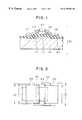
- FIG. 1is a cross sectional view showing a first embodiment of a thin film transistor array substrate including a thin film transistor according to the present invention
- FIG. 2is a schematic plan view of the substrate shown in FIG. 1;
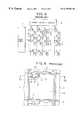
- FIG. 3is a cross sectional view showing an example in which the structure shown in FIG. 1 is applied to a liquid crystal display device;
- FIG. 4is a view showing an example of dimensions when the structure according to the present invention is applied to the thin film transistor array substrate;
- FIG. 5is a circuit diagram showing an example an equivalent circuit of a conventional active matrix liquid crystal display device
- FIG. 6is a plan view showing a portion of an example of a liquid crystal display device including the circuit shown in FIG. 5;
- FIG. 7is a cross sectional view taken along the line VII—VII of FIG. 6;
- FIG. 8Ais a plan view showing an example of a conventional thin film transistor proposed for the purpose of reducing the effect of a photoelectric current
- FIG. 8Bis a plan view showing a second example of the conventional thin film transistor proposed for the same object.
- FIG. 1shows a first embodiment of a thin film transistor according to the present invention.
- a thin film transistor 40 of the embodimentis arranged such that a rectangular gate electrode 42 is formed on a transparent substrate 41 such as a glass (for example, #7059 glass having a refractive index of 1.530 made by Corning Inc.) etc. and an insulation layer 43 (for example, a silicon nitride film exhibiting a refractive index of about 1.85) is formed to cover the upper surface of the substrate 41 and the gate electrode 42 .
- the gate electrode 42is formed of a light shielding conductor metal material such as Al, Cr or the like.
- a semiconductor layer 46composed of amorphous silicon or the like and having a width slightly smaller than that of the gate electrode 42 shown in FIG.
- the gate electrode 42is made larger than the rectangular semiconductor layer 46 in both longitudinal and lateral widths as shown in FIG. 2 and formed to a size capable of covering and concealing the semiconductor layer 46 from the substrate 41 side as well as the line width of the source electrode 49 and the drain electrode 50 (the width denoted by a symbol D in FIG.
- the width in the direction perpendicular to the direction in which a current flowsis made larger than the width d 1 of the semiconductor layer 46 along the same direction.
- the width d 1 of the semiconductor layer 46is formed smaller than the line width D of the source electrode 49 and the drain electrode 50 and the semiconductor layer 46 is formed in such a manner that both the ends of the source electrode 49 and the drain electrode 50 along the line width direction thereof are not connected to each other but the central potions of the source electrode 49 and the drain electrode 50 along the line width direction thereof are connected to each other.
- the width d 2 of the etching stopper layer 44 along the same direction as the above line width directionis made larger than the line width of the source electrode 49 and the drain electrode 50 and smaller than the width d 3 of the gate electrode 42 along the same direction.
- the thin film transistor 40 having the structure of the embodimentis provided by being assembled to a liquid crystal display device in place of the thin film transistor array substrate of the liquid crystal display device shown in FIG. 5 -FIG. 7 and used to drive a liquid crystal likewise the conventional thin film transistor.
- a black mask 53is disposed to a confronting substrate 52 which is disposed in confrontation with the substrate 41 on the on the substrate 41 side thereof, so that it shields the region corresponding to the portion such as the gate electrode 42 , the semiconductor layer 46 , the source electrode 49 , the drain electrode 50 and the like which is different from the region where the orientation of the liquid crystal is controlled.
- a display and a non-displaycan be effected in such a manner that an electric field is applied to the molecules of the liquid crystal by applying a charge to a specific pixel electrode 15 by a specific thin film transistor 40 by imposing a signal to a necessary scan electrode wire G and signal electrode wire.
- the gate electrode 42is formed to the size for covering and concealing the semiconductor layer 46 from the substrate 41 side, even if lights linearly travel upward from the lower side of the substrate 41 as shown by the arrows L 3 in FIG. 3, since the lights are shielded by the light shielding gate electrode 42 , they do not reach the semiconductor layer 46 . Further, even if a light is obliquely incident from the peripheral portion of the gate electrode 42 as shown by the arrow L 4 in FIG. 3, since the light is shielded by the gate electrode 42 , there is few possibility that the light shown by L 4 reaches the semiconductor layer 46 .
- FIG. 4shows an example of the dimension of the respective portions of the thin film transistor having the structure shown in FIG. 1 when it is embodied.
- the structure according to the present inventioncan be realized to an actual thin film transistor array substrate by setting the lateral width of a gate electrode 42′ to 17 ⁇ m, the line width of a right drain electrode 50′ and a left source electrode 49′to 6 ⁇ m, the interval therebetween to 3.0 ⁇ m, the lateral width of the etching stopper layer 44′ to 6 ⁇ m, the width of the source electrode 49′ and the drain electrode 50′ covering the etching stopper layer 44′ to 1.5 ⁇ m, the lateral width of semiconductor layer 46′ to 9 ⁇ m and the longitudinal width thereof to 3 ⁇ m.
Landscapes
- Physics & Mathematics (AREA)
- Nonlinear Science (AREA)
- Engineering & Computer Science (AREA)
- Microelectronics & Electronic Packaging (AREA)
- Mathematical Physics (AREA)
- Chemical & Material Sciences (AREA)
- Crystallography & Structural Chemistry (AREA)
- General Physics & Mathematics (AREA)
- Optics & Photonics (AREA)
- Liquid Crystal (AREA)
- Thin Film Transistor (AREA)
Abstract
Description
Claims (14)
Applications Claiming Priority (2)
| Application Number | Priority Date | Filing Date | Title |
|---|---|---|---|
| JP8-011237 | 1996-01-25 | ||
| JP1123796AJPH09203908A (en) | 1996-01-25 | 1996-01-25 | Thin-film transistor for liquid crystal display device and liquid crystal display device |
Publications (1)
| Publication Number | Publication Date |
|---|---|
| US6278504B1true US6278504B1 (en) | 2001-08-21 |
Family
ID=11772337
Family Applications (1)
| Application Number | Title | Priority Date | Filing Date |
|---|---|---|---|
| US08/787,463Expired - LifetimeUS6278504B1 (en) | 1996-01-25 | 1997-01-22 | Thin film transistor for liquid crystal display device having a semiconductor layer's width smaller than a width of the gate, drain and source electrodes |
Country Status (3)
| Country | Link |
|---|---|
| US (1) | US6278504B1 (en) |
| JP (1) | JPH09203908A (en) |
| KR (1) | KR100359796B1 (en) |
Cited By (24)
| Publication number | Priority date | Publication date | Assignee | Title |
|---|---|---|---|---|
| US20020063841A1 (en)* | 2000-09-08 | 2002-05-30 | Semiconductor Energy Laboratory Co., Ltd. | Liquid crystal display device |
| US20020113930A1 (en)* | 2000-11-02 | 2002-08-22 | Semiconductor Energy Laboratory Co., Ltd. | Liquid crystal display device |
| US6618110B2 (en)* | 2000-08-08 | 2003-09-09 | Lg.Philips Lcd Co., Ltd. | Liquid crystal display and fabricating method thereof |
| US6917392B2 (en)* | 1999-12-22 | 2005-07-12 | Nec Lcd Technologies, Ltd. | Liquid crystal display apparatus of a lateral direction electric field drive type |
| US20060250558A1 (en)* | 2003-02-04 | 2006-11-09 | Plastic Logic Limited | Transistor-controlled display devices |
| US20060273318A1 (en)* | 2005-06-01 | 2006-12-07 | Au Optronics Corp. | Displaying device with photocurrent-reducing structure and method of manufacturing the same |
| US20080129910A1 (en)* | 2002-08-30 | 2008-06-05 | Akiyoshi Fujii | Thin film transistor, liquid crystal display apparatus, manufacturing method of thin film transistor, and manufacturing method of liquid crystal display apparatus |
| CN100449715C (en)* | 2006-01-23 | 2009-01-07 | 友达光电股份有限公司 | Thin film transistor and method of manufacturing the same |
| US20100315570A1 (en)* | 2009-06-11 | 2010-12-16 | Mathew Dinesh C | Portable computer display structures |
| US20110096449A1 (en)* | 2009-10-26 | 2011-04-28 | Mi-Sun Lee | Substrate for a Display Device and Method of Manufacturing the Same |
| US20110103041A1 (en)* | 2009-11-03 | 2011-05-05 | Mathew Dinesh C | Portable computer housing with integral display |
| US20110109829A1 (en)* | 2009-11-10 | 2011-05-12 | Mathew Dinesh C | Methods for fabricating display structures |
| WO2012058536A1 (en)* | 2010-10-29 | 2012-05-03 | Apple Inc. | Camera lens structures and display structures for electronic devices |
| US8467177B2 (en) | 2010-10-29 | 2013-06-18 | Apple Inc. | Displays with polarizer windows and opaque masking layers for electronic devices |
| US8614443B2 (en) | 2011-02-17 | 2013-12-24 | Samsung Display Co., Ltd. | Display apparatus and method of manufacturing the same |
| WO2016082234A1 (en)* | 2014-11-24 | 2016-06-02 | 深圳市华星光电技术有限公司 | Thin film transistor, display device and manufacturing method for thin film transistor |
| CN106066552A (en)* | 2008-11-28 | 2016-11-02 | 株式会社半导体能源研究所 | Liquid crystal display device |
| US10204973B2 (en) | 2014-01-15 | 2019-02-12 | Joled Inc. | Display device and thin-film transistors substrate |
| US20220020841A1 (en)* | 2008-09-19 | 2022-01-20 | Semiconductor Energy Laboratory Co., Ltd. | Semiconductor device |
| US11632448B2 (en) | 2019-12-03 | 2023-04-18 | Apple Inc. | Handheld electronic device |
| US11637919B2 (en) | 2019-12-03 | 2023-04-25 | Apple Inc. | Handheld electronic device |
| US11955559B2 (en) | 2016-04-25 | 2024-04-09 | Sakai Display Products Corporation | Thin film transistor, display device, and thin film transistor manufacturing method |
| US12003657B2 (en) | 2021-03-02 | 2024-06-04 | Apple Inc. | Handheld electronic device |
| US12267449B2 (en) | 2022-03-03 | 2025-04-01 | Apple Inc. | Handheld electronic device |
Families Citing this family (9)
| Publication number | Priority date | Publication date | Assignee | Title |
|---|---|---|---|---|
| JP2001343669A (en)* | 2000-06-02 | 2001-12-14 | Hitachi Ltd | Liquid crystal display |
| KR100508000B1 (en)* | 2002-08-27 | 2005-08-17 | 엘지.필립스 엘시디 주식회사 | The substrate for LCD and method for fabricating the same |
| JP4507540B2 (en)* | 2003-09-12 | 2010-07-21 | カシオ計算機株式会社 | Thin film transistor |
| KR100683664B1 (en)* | 2004-01-06 | 2007-02-15 | 삼성에스디아이 주식회사 | Thin film transistor, method of manufacturing thin film transistor and flat panel display device having same |
| KR101248003B1 (en)* | 2006-05-09 | 2013-03-27 | 엘지디스플레이 주식회사 | The substrate for LCD and method for fabricating of the same |
| JP5442228B2 (en)* | 2008-08-07 | 2014-03-12 | 株式会社ジャパンディスプレイ | Display device and manufacturing method of display device |
| JP2010113253A (en)* | 2008-11-07 | 2010-05-20 | Hitachi Displays Ltd | Display device and method of manufacturing the same |
| WO2011027649A1 (en)* | 2009-09-02 | 2011-03-10 | Semiconductor Energy Laboratory Co., Ltd. | Semiconductor device including a transistor, and manufacturing method of semiconductor device |
| CN109244085A (en)* | 2018-09-27 | 2019-01-18 | 惠科股份有限公司 | Array substrate and display panel |
Citations (9)
| Publication number | Priority date | Publication date | Assignee | Title |
|---|---|---|---|---|
| US5187551A (en)* | 1988-04-30 | 1993-02-16 | Sharp Kabushiki Kaisha | Thin film semiconductor device and liquid crystal display apparatus thereof for preventing irradiated light from reaching the semiconductor layers |
| JPH05293823A (en) | 1992-04-21 | 1993-11-09 | Nippon Electric Glass Co Ltd | Bmc formed body |
| US5286659A (en)* | 1990-12-28 | 1994-02-15 | Sharp Kabushiki Kaisha | Method for producing an active matrix substrate |
| US5471330A (en)* | 1993-07-29 | 1995-11-28 | Honeywell Inc. | Polysilicon pixel electrode |
| US5473168A (en)* | 1993-04-30 | 1995-12-05 | Sharp Kabushiki Kaisha | Thin film transistor |
| US5474941A (en)* | 1990-12-28 | 1995-12-12 | Sharp Kabushiki Kaisha | Method for producing an active matrix substrate |
| US5614731A (en)* | 1993-03-15 | 1997-03-25 | Kabushiki Kaisha Toshiba | Thin-film transistor element having a structure promoting reduction of light-induced leakage current |
| US5712494A (en)* | 1995-03-22 | 1998-01-27 | Kabushiki Kaisha Toshiba | Thin film field effect transistor having an extension portion acting as a light shield and back gate |
| US5929958A (en)* | 1995-03-17 | 1999-07-27 | Hitachi, Ltd. | Liquid crystal display device with wide viewing angle characteristics |
Family Cites Families (2)
| Publication number | Priority date | Publication date | Assignee | Title |
|---|---|---|---|---|
| US5327001A (en)* | 1987-09-09 | 1994-07-05 | Casio Computer Co., Ltd. | Thin film transistor array having single light shield layer over transistors and gate and drain lines |
| JPH02199842A (en)* | 1989-01-27 | 1990-08-08 | Nec Corp | Manufacture of thin-film field-effect transistor element |
- 1996
- 1996-01-25JPJP1123796Apatent/JPH09203908A/enactivePending
- 1997
- 1997-01-22KRKR1019970001794Apatent/KR100359796B1/ennot_activeExpired - Lifetime
- 1997-01-22USUS08/787,463patent/US6278504B1/ennot_activeExpired - Lifetime
Patent Citations (9)
| Publication number | Priority date | Publication date | Assignee | Title |
|---|---|---|---|---|
| US5187551A (en)* | 1988-04-30 | 1993-02-16 | Sharp Kabushiki Kaisha | Thin film semiconductor device and liquid crystal display apparatus thereof for preventing irradiated light from reaching the semiconductor layers |
| US5286659A (en)* | 1990-12-28 | 1994-02-15 | Sharp Kabushiki Kaisha | Method for producing an active matrix substrate |
| US5474941A (en)* | 1990-12-28 | 1995-12-12 | Sharp Kabushiki Kaisha | Method for producing an active matrix substrate |
| JPH05293823A (en) | 1992-04-21 | 1993-11-09 | Nippon Electric Glass Co Ltd | Bmc formed body |
| US5614731A (en)* | 1993-03-15 | 1997-03-25 | Kabushiki Kaisha Toshiba | Thin-film transistor element having a structure promoting reduction of light-induced leakage current |
| US5473168A (en)* | 1993-04-30 | 1995-12-05 | Sharp Kabushiki Kaisha | Thin film transistor |
| US5471330A (en)* | 1993-07-29 | 1995-11-28 | Honeywell Inc. | Polysilicon pixel electrode |
| US5929958A (en)* | 1995-03-17 | 1999-07-27 | Hitachi, Ltd. | Liquid crystal display device with wide viewing angle characteristics |
| US5712494A (en)* | 1995-03-22 | 1998-01-27 | Kabushiki Kaisha Toshiba | Thin film field effect transistor having an extension portion acting as a light shield and back gate |
Cited By (71)
| Publication number | Priority date | Publication date | Assignee | Title |
|---|---|---|---|---|
| US6917392B2 (en)* | 1999-12-22 | 2005-07-12 | Nec Lcd Technologies, Ltd. | Liquid crystal display apparatus of a lateral direction electric field drive type |
| US6864928B2 (en) | 2000-08-08 | 2005-03-08 | Lg.Philips Lcd Co., Ltd. | Liquid crystal display having a drain electrode with a plurality of protrusions and a fabrication method thereof |
| US6618110B2 (en)* | 2000-08-08 | 2003-09-09 | Lg.Philips Lcd Co., Ltd. | Liquid crystal display and fabricating method thereof |
| US20040027506A1 (en)* | 2000-08-08 | 2004-02-12 | Lg. Philips Lcd Co., Ltd. | Liquid crystal display and fabricating method thereof |
| US7248320B2 (en) | 2000-09-08 | 2007-07-24 | Semiconductor Energy Laboratory Co., Ltd. | Liquid crystal display device |
| US8587741B2 (en) | 2000-09-08 | 2013-11-19 | Semiconductor Energy Laboratory Co., Ltd. | Liquid crystal display device |
| US6734924B2 (en)* | 2000-09-08 | 2004-05-11 | Semiconductor Energy Laboratory Co., Ltd. | Liquid crystal display device |
| US8102480B2 (en) | 2000-09-08 | 2012-01-24 | Semiconductor Energy Laboratory Co., Ltd. | Liquid crystal display device |
| US20020063841A1 (en)* | 2000-09-08 | 2002-05-30 | Semiconductor Energy Laboratory Co., Ltd. | Liquid crystal display device |
| US20100039574A1 (en)* | 2000-09-08 | 2010-02-18 | Semiconductor Energy Laboratory Co., Ltd. | Liquid Crystal Display Device |
| US9798204B2 (en) | 2000-09-08 | 2017-10-24 | Semiconductor Energy Laboratory Co., Ltd. | Liquid crystal display device |
| US7609332B2 (en) | 2000-09-08 | 2009-10-27 | Semiconductor Energy Laboratory Co., Ltd. | Liquid crystal display device |
| US20040160540A1 (en)* | 2000-09-08 | 2004-08-19 | Semiconductor Energy Laboratory Co., Ltd. | Liquid crystal display device |
| US7554642B2 (en) | 2000-11-02 | 2009-06-30 | Semiconductor Energy Laboratory Co., Ltd. | Liquid crystal display device having particular configuration of pixel electrodes |
| US7446840B2 (en) | 2000-11-02 | 2008-11-04 | Semiconductor Energy Laboratory Co., Ltd. | Liquid crystal display device having particular configuration of pixel electrodes |
| US20080117375A1 (en)* | 2000-11-02 | 2008-05-22 | Semiconductor Energy Laboratory Co., Ltd. | Liquid crystal display device |
| US8059246B2 (en) | 2000-11-02 | 2011-11-15 | Semiconductor Energy Laboratory Co., Ltd. | Liquid crystal display device having particular pixel electrodes configuration |
| US7167226B2 (en) | 2000-11-02 | 2007-01-23 | Semiconductor Energy Laboratory Co., Ltd. | Liquid crystal display device having particular configuration of pixel electrodes |
| US20090268111A1 (en)* | 2000-11-02 | 2009-10-29 | Semiconductor Energy Laboratory Co., Ltd. | Liquid Crystal Display Device |
| US20020113930A1 (en)* | 2000-11-02 | 2002-08-22 | Semiconductor Energy Laboratory Co., Ltd. | Liquid crystal display device |
| US20050099566A1 (en)* | 2000-11-02 | 2005-05-12 | Semiconductor Energy Laboratory Co., Ltd. | Liquid crystal display device |
| US20080129910A1 (en)* | 2002-08-30 | 2008-06-05 | Akiyoshi Fujii | Thin film transistor, liquid crystal display apparatus, manufacturing method of thin film transistor, and manufacturing method of liquid crystal display apparatus |
| US20060250558A1 (en)* | 2003-02-04 | 2006-11-09 | Plastic Logic Limited | Transistor-controlled display devices |
| US8400576B2 (en)* | 2003-02-04 | 2013-03-19 | Plastic Logic Limited | Transistor-controlled display devices |
| US8581259B2 (en)* | 2005-06-01 | 2013-11-12 | Au Optronics Corp. | Displaying device with photocurrent-reducing structure and method of manufacturing the same |
| US20060273318A1 (en)* | 2005-06-01 | 2006-12-07 | Au Optronics Corp. | Displaying device with photocurrent-reducing structure and method of manufacturing the same |
| CN100449715C (en)* | 2006-01-23 | 2009-01-07 | 友达光电股份有限公司 | Thin film transistor and method of manufacturing the same |
| US12250855B2 (en)* | 2008-09-19 | 2025-03-11 | Semiconductor Energy Laboratory Co., Ltd. | Semiconductor device |
| US20220020841A1 (en)* | 2008-09-19 | 2022-01-20 | Semiconductor Energy Laboratory Co., Ltd. | Semiconductor device |
| US10424674B2 (en) | 2008-11-28 | 2019-09-24 | Semiconductor Energy Laboratory Co., Ltd. | Liquid crystal display device |
| US11869978B2 (en) | 2008-11-28 | 2024-01-09 | Semiconductor Energy Laboratory Co., Ltd. | Liquid crystal display device |
| US10008608B2 (en) | 2008-11-28 | 2018-06-26 | Semiconductor Energy Laboratory Co., Ltd. | Liquid crystal display device |
| CN106066552A (en)* | 2008-11-28 | 2016-11-02 | 株式会社半导体能源研究所 | Liquid crystal display device |
| US10985282B2 (en) | 2008-11-28 | 2021-04-20 | Semiconductor Energy Laboratory Co., Ltd. | Liquid crystal display device |
| US20100315570A1 (en)* | 2009-06-11 | 2010-12-16 | Mathew Dinesh C | Portable computer display structures |
| US12189424B2 (en) | 2009-06-11 | 2025-01-07 | Apple Inc. | Portable computer display structures |
| US10353432B2 (en) | 2009-06-11 | 2019-07-16 | Apple Inc. | Portable computer display structures |
| US8711304B2 (en) | 2009-06-11 | 2014-04-29 | Apple Inc. | Portable computer display structures |
| US11740658B2 (en) | 2009-06-11 | 2023-08-29 | Apple Inc. | Portable computer display structures |
| US8395722B2 (en) | 2009-06-11 | 2013-03-12 | Apple Inc. | Portable computer display structures |
| US8456586B2 (en) | 2009-06-11 | 2013-06-04 | Apple Inc. | Portable computer display structures |
| US8866989B2 (en) | 2009-06-11 | 2014-10-21 | Apple Inc. | Portable computer display structures |
| US11003213B2 (en) | 2009-06-11 | 2021-05-11 | Apple Inc. | Portable computer display structures |
| US8854564B2 (en) | 2009-10-26 | 2014-10-07 | Samsung Display Co., Ltd. | Substrate for a display device and method of manufacturing the same |
| US8520158B2 (en)* | 2009-10-26 | 2013-08-27 | Samsung Display Co., Ltd. | Substrate for a display device and method of manufacturing the same |
| US20110096449A1 (en)* | 2009-10-26 | 2011-04-28 | Mi-Sun Lee | Substrate for a Display Device and Method of Manufacturing the Same |
| US8408780B2 (en) | 2009-11-03 | 2013-04-02 | Apple Inc. | Portable computer housing with integral display |
| US20110103041A1 (en)* | 2009-11-03 | 2011-05-05 | Mathew Dinesh C | Portable computer housing with integral display |
| US9575354B2 (en) | 2009-11-10 | 2017-02-21 | Apple Inc. | Methods for fabricating display structures |
| US8743309B2 (en) | 2009-11-10 | 2014-06-03 | Apple Inc. | Methods for fabricating display structures |
| US20110109829A1 (en)* | 2009-11-10 | 2011-05-12 | Mathew Dinesh C | Methods for fabricating display structures |
| US8767141B2 (en) | 2009-11-10 | 2014-07-01 | Apple Inc. | Methods for fabricating display structures |
| US9069525B2 (en) | 2009-11-10 | 2015-06-30 | Apple Inc. | Methods for fabricating display structures |
| US10261540B2 (en) | 2009-11-10 | 2019-04-16 | Apple Inc. | Methods for fabricating display structures |
| US10983390B2 (en) | 2009-11-10 | 2021-04-20 | Apple Inc. | Methods for fabricating display structures |
| US8467177B2 (en) | 2010-10-29 | 2013-06-18 | Apple Inc. | Displays with polarizer windows and opaque masking layers for electronic devices |
| US10571957B2 (en) | 2010-10-29 | 2020-02-25 | Apple Inc. | Displays with polarizer windows and opaque masking layers for electronic devices |
| US9372505B2 (en) | 2010-10-29 | 2016-06-21 | Apple Inc. | Displays with polarizer windows and opaque masking layers for electronic devices |
| US9143668B2 (en) | 2010-10-29 | 2015-09-22 | Apple Inc. | Camera lens structures and display structures for electronic devices |
| US11188118B2 (en) | 2010-10-29 | 2021-11-30 | Apple Inc. | Displays with polarizer windows and opaque masking layers for electronic devices |
| WO2012058536A1 (en)* | 2010-10-29 | 2012-05-03 | Apple Inc. | Camera lens structures and display structures for electronic devices |
| US10009525B2 (en) | 2010-10-29 | 2018-06-26 | Apple Inc. | Camera lens structures and display structures for electronic devices |
| US8614443B2 (en) | 2011-02-17 | 2013-12-24 | Samsung Display Co., Ltd. | Display apparatus and method of manufacturing the same |
| US10204973B2 (en) | 2014-01-15 | 2019-02-12 | Joled Inc. | Display device and thin-film transistors substrate |
| US10084013B2 (en) | 2014-11-24 | 2018-09-25 | Shenzhen China Star Optoelectronics Technology Co., Ltd | Thin-film transistor, display device, and method for manufacturing thin-film transistor |
| WO2016082234A1 (en)* | 2014-11-24 | 2016-06-02 | 深圳市华星光电技术有限公司 | Thin film transistor, display device and manufacturing method for thin film transistor |
| US11955559B2 (en) | 2016-04-25 | 2024-04-09 | Sakai Display Products Corporation | Thin film transistor, display device, and thin film transistor manufacturing method |
| US11637919B2 (en) | 2019-12-03 | 2023-04-25 | Apple Inc. | Handheld electronic device |
| US11632448B2 (en) | 2019-12-03 | 2023-04-18 | Apple Inc. | Handheld electronic device |
| US12003657B2 (en) | 2021-03-02 | 2024-06-04 | Apple Inc. | Handheld electronic device |
| US12267449B2 (en) | 2022-03-03 | 2025-04-01 | Apple Inc. | Handheld electronic device |
Also Published As
| Publication number | Publication date |
|---|---|
| JPH09203908A (en) | 1997-08-05 |
| KR970059803A (en) | 1997-08-12 |
| KR100359796B1 (en) | 2003-01-15 |
Similar Documents
| Publication | Publication Date | Title |
|---|---|---|
| US6278504B1 (en) | Thin film transistor for liquid crystal display device having a semiconductor layer's width smaller than a width of the gate, drain and source electrodes | |
| US7023502B2 (en) | Semiconductor device having light-shielded thin film transistor | |
| KR0156766B1 (en) | Thin film transistor and display device using the same | |
| US5835168A (en) | Active matrix liquid crystal having capacitance electrodes connected to pixel electrodes | |
| KR100635940B1 (en) | Vertically Aligned Liquid Crystal Display | |
| KR100878379B1 (en) | Liquid crystal display | |
| US5598012A (en) | Thin-film transistor with wide gate electrode and liquid crystal display incorporating same | |
| EP0186036A2 (en) | Liquid crystal display device | |
| KR100611840B1 (en) | Liquid crystal device, active matrix substrate, display device, and electronic equipment | |
| US6064091A (en) | Thin film transistors having an active region composed of intrinsic and amorphous semiconducting layers | |
| US7123323B2 (en) | Liquid crystal display device with conductive light shielding film and contact holes | |
| KR100474529B1 (en) | Reflective liquid crystal display device and its manufacturing method | |
| US6326641B1 (en) | Liquid crystal display device having a high aperture ratio | |
| US7268839B2 (en) | Array substrate comprising an island shaped drain electrode enclosed by the source electrode and liquid crystal display device including the same | |
| US6611311B1 (en) | Active-matrix display screen | |
| EP1279997B1 (en) | Liquid crystal display device | |
| JP3750303B2 (en) | Liquid crystal display | |
| KR19990007458A (en) | Thin Film Transistors for Liquid Crystal Displays | |
| JP2777545B2 (en) | Active matrix liquid crystal display | |
| JP3156179B2 (en) | Liquid crystal display device | |
| JPH09325360A (en) | Liquid crystal display | |
| JP2677248B2 (en) | Active matrix liquid crystal display panel | |
| JPH07333655A (en) | Active matrix type display device | |
| JPH09244044A (en) | Liquid crystal display | |
| JPH11183932A (en) | Active matrix liquid crystal display |
Legal Events
| Date | Code | Title | Description |
|---|---|---|---|
| AS | Assignment | Owner name:FRONTEC INCORPORATED, JAPAN Free format text:ASSIGNMENT OF ASSIGNORS INTEREST;ASSIGNOR:SUNG, CHAE GEE;REEL/FRAME:008554/0410 Effective date:19970512 | |
| AS | Assignment | Owner name:LG. PHILIPS LCD CO., LTD., KOREA, REPUBLIC OF Free format text:ASSIGNMENT OF ASSIGNORS INTEREST;ASSIGNOR:FRONTEC INCORPORATED;REEL/FRAME:011390/0346 Effective date:20001201 | |
| STCF | Information on status: patent grant | Free format text:PATENTED CASE | |
| FEPP | Fee payment procedure | Free format text:PAYOR NUMBER ASSIGNED (ORIGINAL EVENT CODE: ASPN); ENTITY STATUS OF PATENT OWNER: LARGE ENTITY | |
| FPAY | Fee payment | Year of fee payment:4 | |
| AS | Assignment | Owner name:LG DISPLAY CO., LTD., KOREA, REPUBLIC OF Free format text:CHANGE OF NAME;ASSIGNOR:LG PHILIPS CO., LTD.;REEL/FRAME:020976/0785 Effective date:20080229 Owner name:LG DISPLAY CO., LTD.,KOREA, REPUBLIC OF Free format text:CHANGE OF NAME;ASSIGNOR:LG PHILIPS CO., LTD.;REEL/FRAME:020976/0785 Effective date:20080229 | |
| FPAY | Fee payment | Year of fee payment:8 | |
| FEPP | Fee payment procedure | Free format text:PAYER NUMBER DE-ASSIGNED (ORIGINAL EVENT CODE: RMPN); ENTITY STATUS OF PATENT OWNER: LARGE ENTITY Free format text:PAYOR NUMBER ASSIGNED (ORIGINAL EVENT CODE: ASPN); ENTITY STATUS OF PATENT OWNER: LARGE ENTITY | |
| FPAY | Fee payment | Year of fee payment:12 |