US6277728B1 - Multilevel interconnect structure with low-k dielectric and method of fabricating the structure - Google Patents
Multilevel interconnect structure with low-k dielectric and method of fabricating the structureDownload PDFInfo
- Publication number
- US6277728B1 US6277728B1US09/375,561US37556199AUS6277728B1US 6277728 B1US6277728 B1US 6277728B1US 37556199 AUS37556199 AUS 37556199AUS 6277728 B1US6277728 B1US 6277728B1
- Authority
- US
- United States
- Prior art keywords
- copper
- layer
- photoresist
- metal
- depositing
- Prior art date
- Legal status (The legal status is an assumption and is not a legal conclusion. Google has not performed a legal analysis and makes no representation as to the accuracy of the status listed.)
- Expired - Lifetime
Links
Images


Classifications
- H—ELECTRICITY
- H01—ELECTRIC ELEMENTS
- H01L—SEMICONDUCTOR DEVICES NOT COVERED BY CLASS H10
- H01L21/00—Processes or apparatus adapted for the manufacture or treatment of semiconductor or solid state devices or of parts thereof
- H01L21/70—Manufacture or treatment of devices consisting of a plurality of solid state components formed in or on a common substrate or of parts thereof; Manufacture of integrated circuit devices or of parts thereof
- H01L21/71—Manufacture of specific parts of devices defined in group H01L21/70
- H01L21/768—Applying interconnections to be used for carrying current between separate components within a device comprising conductors and dielectrics
- H01L21/76801—Applying interconnections to be used for carrying current between separate components within a device comprising conductors and dielectrics characterised by the formation and the after-treatment of the dielectrics, e.g. smoothing
- H01L21/7682—Applying interconnections to be used for carrying current between separate components within a device comprising conductors and dielectrics characterised by the formation and the after-treatment of the dielectrics, e.g. smoothing the dielectric comprising air gaps
- H—ELECTRICITY
- H01—ELECTRIC ELEMENTS
- H01L—SEMICONDUCTOR DEVICES NOT COVERED BY CLASS H10
- H01L23/00—Details of semiconductor or other solid state devices
- H01L23/48—Arrangements for conducting electric current to or from the solid state body in operation, e.g. leads, terminal arrangements ; Selection of materials therefor
- H01L23/482—Arrangements for conducting electric current to or from the solid state body in operation, e.g. leads, terminal arrangements ; Selection of materials therefor consisting of lead-in layers inseparably applied to the semiconductor body (electrodes)
- H01L23/485—Arrangements for conducting electric current to or from the solid state body in operation, e.g. leads, terminal arrangements ; Selection of materials therefor consisting of lead-in layers inseparably applied to the semiconductor body (electrodes) consisting of layered constructions comprising conductive layers and insulating layers, e.g. planar contacts
- H—ELECTRICITY
- H01—ELECTRIC ELEMENTS
- H01L—SEMICONDUCTOR DEVICES NOT COVERED BY CLASS H10
- H01L2924/00—Indexing scheme for arrangements or methods for connecting or disconnecting semiconductor or solid-state bodies as covered by H01L24/00
- H01L2924/0001—Technical content checked by a classifier
- H01L2924/0002—Not covered by any one of groups H01L24/00, H01L24/00 and H01L2224/00
Definitions
- the present inventionrelates to a semiconductor multilevel interconnect structures exhibiting a low RC time delay and which take less time to fabricate. More particularly, the present invention relates to a semiconductor multilevel interconnect structure made of metals having a low resistivity and insulators having a low dielectric constant k, and to a method of fabricating the multilevel interconnect structure with a low-k dielectric.
- the metalWhen a metal is used to form the interconnect layers of conductors, the metal is usually deposited on the semiconductor by sputtering, chemical vapor deposition (CVD), or evaporation.
- the CVD processforms a non-volatile solid film on a substrate by the reaction of vapor phase chemicals that contain the desired constituents.
- the metals that are commonly used for the interconnect layersare aluminum and its alloys, although other conductive metals and materials can also be used, with copper being a recent preference,
- the metal layersare typically deposited over dielectric materials, such as silicon dioxide. Parallel plate capacitive effects can be observed with a conductive interconnect structure.
- Togo et al.“A Gate-side Air-gap Structure (GAS) to Reduce the Parasitic Capacitance in MOSFETs”, 1996 Symposium on VLSI Technology, Digest of Technical Papers, pp. 38-39.
- Togo et aloutlines a transistor structure in which the sidewalls of the gate structure are surrounded by an air gap.
- a silicon nitride sidewallis first fabricated that surrounds the gate.
- a layer of silicon dioxideis formed around the silicon nitride sidewall.
- the silicon nitride sidewallis removed by a wet etching process to form an air gap between the gate structure and the silicon dioxide.
- Anand et aloutlines a metal interconnect structure in which layers of a gas are formed between thin layers of silicon dioxide.
- the thin layers of silicon dioxidehave metal interconnect layers deposited on them.
- the processbegins when layers of carbon are formed on a surface and trenches are formed for future interconnections.
- An interconnect metal layeris formed in the carbon trenches and a thin layer of silicon dioxide is sputter-deposited. Oxygen is then furnace ashed into the carbon layer through diffusion and the oxygen reacts with the carbon to form carbon dioxide. This process is repeated to form the interconnect structure of the device under fabrication.
- Togo et alclaims to reduce the capacitance associated with the interconnect layers by reducing the dielectric constant of the materials between the interconnect layers, Togo et al only provides a low dielectric material (air) around the gate contact of a transistor. Also, Togo et al does not disclose an interconnect structure that has reduced resistivity.
- Anand et alclaims to reduce the capacitance associated with the interconnect layers by reducing the dielectric constant of the materials between the interconnect layers, Anand et al adds complexity to the semiconductor fabrication process because carbon is used in the process, which is not typically used in the manufacture of semiconductor devices. The method of Anand et al does not disclose an interconnect structure that has reduced resistivity.
- the needexists for a semiconductor interconnect structure with reduced capacitance and reduced resistivity, thereby decreasing the RC time delay associated with the interconnect layers.
- the needalso exists for a method of fabricating such a structure using standard fabrication steps in conjunction with commercially available processing equipment.
- the power dissipationis approximately represented by:
- fthe clock frequency
- clock distributioncan account for up to 40% of the total power dissipation in high-performance wireless computing and communication systems.
- the deposition time of dielectric films in a multilevel interconnect structureis minimized by reducing the number of dielectric deposition cycles.
- the number of dielectric deposition cyclesis reduced to one.
- the multilevel interconnect structureis built using sacrificial photoresist layers, followed by a single dielectric layer deposition cycle.
- the present inventionis directed to a multilevel interconnect semiconductor structure having a low-k dielectric outer coating and to a method of fabricating the structure.
- the interconnect structureis fabricated using typical fabrication steps, materials, and machines.
- the methodin its broadest form, comprises the steps of depositing a layer of photoresist on a substrate assembly, etching the photoresist to form openings, depositing a metal layer on the photoresist layer so as to fill the openings, and removing the photoresist layer by, for example, ashing in an oxygen plasma.
- An upper level conductive metal layeris supported by the metal which filled the openings formed in the photoresist to form a multilevel metallized interconnect structure.
- the upper level of the interconnect structureis then coated with a low-k dielectric film.
- the conductive layerspreferably comprise copper, and the single dielectric deposition is preferably in the form of a layer of an aerogel or xerogel.
- the present inventionrepresents significant advantages over the prior art. Because the air (gas) spaces between the conductive interconnect layers are formed by removing layers of photoresist, no extra material need be introduced into the semiconductor manufacturing process. Also, because the conductive interconnect layers are surrounded by air, the plate capacitance of the interconnect structure is reduced. Furthermore, because a low resistive material such as copper is used for the conductive interconnect layers, the layers may be electroplated or electroless plated at low temperatures.
- Reducing the dielectric constant of the inter-level dielectricimproves interconnect signal delay and reduces AC power consumption. Also, the total process time just for the deposition of dielectrics at multiple levels can exceed 200 hours. Therefore, reducing the time for the deposition of dielectric layers is a significant advantage.
- FIG. 1is a cross-sectional view of a substrate assembly on which a layer of photoresist has been deposited, masked, hardened, and etched;
- FIG. 2is a cross-sectional view of the substrate assembly of FIG. 1 on which a bilayer adhesion promoter/diffusion barrier has been deposited on the etched photoresist layer;
- FIG. 3is a cross-sectional view of the substrate assembly of FIG. 2 on which a metal layer has been deposited on the bilayer adhesion promoter/diffusion barrier;
- FIG. 4is a cross-sectional view of the substrate assembly of FIG. 3 following removal of excess metal from the metal layer to form metal plugs;
- FIG. 5is a cross-sectional view of the substrate assembly of FIG. 4 on which a photoresist layer has been deposited, masked, hardened, and etched on the promoter layer and metal plug;
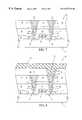
- FIG. 6is a cross-sectional view of the substrate assembly of FIG. 5 on which a bilayer adhesion promoter/diffusion barrier and a first metal layer have been deposited on the etched photoresist layer;
- FIG. 7is a cross-sectional view of the substrate assembly of FIG. 6 following the removal of excess metal from the first metal layer;
- FIG. 8is a cross sectional view of the substrate assembly of FIG. 7 following the addition of a photoresist layer, a bilayer adhesion promoter/diffusion barrier, a metal plug, and a second metal layer onto the etched photoresist layer and the first metal layer;
- FIG. 9is a cross-sectional view of the substrate assembly of FIG. 8 following the removal of the photoresist layers to form gaps between the bilayers of adhesion promoter/diffusion barrier and the underlying substrate assembly;
- FIG. 10is a cross-sectional view of another embodiment of a substrate assembly on which a layer of photoresist has been deposited, masked, hardened, and etched;
- FIG. 11is a cross-sectional view of the substrate assembly of FIG. 10 on which a bilayer adhesion promoter/diffusion barrier has been deposited on the layer of photoresist and on which a metal layer has been deposited on the bilayer;
- FIG. 12is a cross-sectional view of the substrate assembly of FIG. 11 following removal of excess metal from the metal layer to form metal plugs and then coated with a low-k dielectric film.
- a bilayer adhesion promoter/diffusion barriermeans that the bilayer functions to enhance adhesion of the metal layer to the structure and to minimize the diffusion of metal from the metal layer into dielectric material.
- the present inventionrelates to the provision of an interconnect structure which has an improved RC response for high speed signal transmission and which is relatively easy to construct:
- methods of depositing aerogels, xerogels and other spin-coated dielectric materials used as interconnect dielectronicsoften require complicated, extensive processing.
- the low-density SiO 2 xerogel films which are often used to insulate an interconnect structureare prepared by a sol-gel process which offers the precise control of microstructure (pore size, pore volume, and surface area).
- a typical processinvolves a spin coating (20 sec), aging/washing (24 hours), surface modification (12 hours), and drying/thermal treatment (2 hours).
- the deposition time of dielectric filmsis minimized by reducing the number of dielectric deposition cycles.
- the number of dielectric deposition cyclesis reduced to one.
- the multilayer metallizationis built using sacrificial photoresist layers, followed by a single dielectric deposition cycle.
- the resultant interconnect structurehas good high speed signal transmission properties because of lowered RC effects.
- Low-k dielectric materialsincluding fluorine-doped SiO 2 , polymers and aerogels which could be used as an interconnect insulator are shown in the following Table. As shown, low-k dielectrics have a dielectric constant less than [or equal to] 4.5.
- aerogelspossess the lowest dielectric constant. Aerogels and also xerogels have a dielectric constant of between 1.1 and 2.0, and also the highest thermal stability (900° C.). Therefore, aerogels and xerogels are preferred for use in accordance with the present invention in ULSI technology. It should also be noted that air has the lowest dielectric constant of 1.0.
- a suitable dielectric material for use in the present inventionhas a dielectric constant of from about 1 to about 2.5.
- a preferred dielectric constant rangeis from about 1 to about 2.0.
- Other properties of suitable low k-materialare no or low moisture absorption, thermal stability, and mechanical stability to be compatible with chem-mechanical planarization process.
- the materialshould be compatible with low & high temperature chip pull off, such that it contains no residues that may outgas during later process at high temperature or at pull off.
- the materialalso preferably has a glass transition (Tg) temperature of >350° C., a high breakdown field strength of >5MV/cm, and a low leakage current of ⁇ 1nA @ use voltage.
- the assembly 30includes a substrate layer 32 , which is the lowest layer of semiconductor material on a wafer and additional layers or structures formed thereon.
- a Local Oxidation of Silicon (LOCOS) processis performed on the substrate layer 32 to provide a layer of gate oxide 33 and device separating field oxide regions 34 formed of, for example, SiO 2 .
- a polysilicon layer 36is deposited and etched to provide a contact area, typically for the gate terminal G of a transistor.
- An isolation insulating spacer 37may be formed along the sides of layer 36 using conventional techniques. Impurities are diffused into the substrate 34 through suitable masks to form diffusion areas 38 .
- the diffusion areas 38provide the source S and drain D terminals of the transistor.
- Silicide layers 40are formed on the diffusion areas 38 .
- the silicide layers 40are formed by depositing a refractory metal such as titanium, platinum, palladium, cobalt, or tungsten on polysilicon. The metal/silicon alloy is then sintered to form the silicide layers 40 .
- the substrate assembly 30is then ready for metallization.
- a first layer of photoresist 42is deposited on the substrate assembly 30 and is masked, hardened, and etched to define openings 43 for contact plugs.
- the photoresist layer 42is hardened by baking the substrate assembly 30 at a temperature typically below 100 ° C.
- FIG. 2shows the substrate assembly 30 of FIG. 1 after a bilayer adhesion promoter/diffusion barrier 44 is deposited by, for example, sputtering onto the surface of the etched photoresist layer 42 . Ionized sputtering is preferred to provide effective coverage of the sidewalls of deep openings. A chemical vapor deposition (CVD) process may also be used to deposit the bilayer adhesion promoter/diffusion barrier 44 .
- CVDchemical vapor deposition
- the bilayer adhesion promoter/diffusion barrier 44can be, among other substances, titanium/copper, chromium/copper, titanium nitride/copper, tantalum/copper, W/copper or WN/copper. Typical thickness is 10 to 20 nm for the adhesive layer and 20 to 30 nm for the copper to be used as a plating base.
- the bilayercan be deposited as two layers.
- the bilayercan be simultaneously deposited from two different sources, e,g., two targets would be used in an ionized sputtering process, or two gas sources could be used in a CVD process.
- adhesion promotor/diffusion barrier 44may be eliminated if a CVD process is used as discussed below for deposition of conducting metal such as copper and aluminum alloys. This step may also be eliminated when deposition techniques such as high-rate magnetron sputtering or evaporation are employed to produce a conducting metal layer as described below.
- a metal layer 46is formed, for example, by plating on the bilayer adhesion promoter/diffusion barrier 44 .
- the metal layer 46is preferably cooper, which can be electroplated or electroless plated on the substrate assembly 30 at a process temperature around 30° C.
- a thick copper film(0.5 to 1.0 micron thick) preferably is deposited.
- the metal layer 46may also be deposited using a CVD process. As noted, if the metal layer 46 is deposited by a CVD process or by high-rate magnetron sputtering or by evaporation, the bilayer adhesion promotor/diffusion barrier 44 may optionally be eliminated.
- the excess metal from the metal layer 46 and the excess bilayer adhesion promoter/diffusion barrier 44are next removed through mechanical abrasion, for example, by chemical mechanical polishing (CMP), to form metal plugs 48 , as shown in FIG. 4 .
- CMPchemical mechanical polishing
- the substrate assembly 30is planar after the removal of the excess metal.
- the remaining portions of the bilayer adhesion promoter/barrier 44define receptacles 45 , in which the metal plugs 48 are located.
- a second photoresist layer 50is next deposited onto the bilayer adhesion promoter/barrier 44 and the metal plugs 48 as shown in FIG. 5 .
- the photoresist layer 50is masked, hardened, and etched to define openings 51 for a metal layer which is aligned with the plugs 48 .
- FIG. 6shows a bilayer adhesion promoter/barrier 52 deposited on the etched photoresist layer 50 and metal plugs 48 and a second metal layer 54 plated on the bilayer adhesion promoter/barrier 52 .
- a portion of the metalfills the openings 51 forming contacts 53 .
- the second metal layer 54is deposited, for example, by electroplating using a plating base. Alternately, a plating base is not needed when metal layer 54 is deposited by CVD, high-rate magnetron sputtering, or evaporation, as was noted above for metal layer 46 .
- excess metal from the second metal layer 54 and excess bilayer adhesion promoter/barrier 52are next removed by mechanical abrasion, such as chemical mechanical polishing (CMP).
- CMPchemical mechanical polishing
- FIG. 8illustrates the substrate assembly 30 of FIG. 7 after (i) photoresist layer 62 is deposited, hardened and etched, (ii) a bilayer adhesion promoter/diffusion barrier 64 is deposited and CMP planarized, and (iii) a third metal layer 70 is deposited onto the substrate assembly 30 .
- the substrate assembly 30 in FIG. 8has been mechanically polished to remove the excess metal layer 70 and the remaining portions of the bilayer adhesion promoter/diffusion barrier 64 to form metal plug 66 in receptacle 68 .
- the third metal layer 70forms contact 72 .
- the surface 54is in contact with another metal plug and receptacle or other assembly component which is not shown in the cross-sectional view of FIG. 8 .
- the steps of applying a patterned photoresist layer, a bilayer adhesion promotor/diffusion barrier 52 (sometimes optional as noted above), and another metal layer, as described with reference to FIGS. 5 to 8 ,can be repeated to build up more metal layers, as needed.
- FIG. 9shows a resulting substrate assembly 30 of FIG. 8 with the first metal layer 48 , the second metal layer 54 and the third metal layer 70 formed.
- the photoresist layers 42 , 50 and 62are next removed by, for example, ashing in oxygen plasma to form air gaps 56 .
- the metal layers 54 and 70are supported by columns 60 and 74 formed by the combination of the metal plugs 48 and the contacts 53 and 72 .
- the air gaps 56have a dielectric constant of 1, thereby reducing the residual capacitance of the resulting interconnected structure.
- the overall RC time constant of the resulting interconnected structureis reduced.
- a suitable bilayer adhesion promoter/diffusion barriermay deposited over the entire structure in one step by, for example, sputtering. Ionized sputtering is preferred to provide effective coverage of the sidewalls of deep openings. Also, a chemical vapor deposition (CVD) process or electroless' plating may be used to deposit the bilayer adhesion promoter/diffusion barrier.
- CVDchemical vapor deposition
- the multilevel metallized interconnect structure of FIG. 9is then coated with a low-k dielectric film 94 in one step.
- This one stepmay be a sol-gel method, a CVD, a spin-on process, or a vapor deposition process.
- the low-k dielectric film 94is planarized.
- preferred materials for film 94are those listed in the table above having a low dielectric constant, preferably between about 1 and about 2.5 and most preferably between about 1 and about 2, with aerogels and xerogels being particularly prefered.
- FIGS. 10 to 12Another embodiment of the invention is shown in FIGS. 10 to 12 . In this embodiment the invention is applied to creating upper levels of interconnects which may be used for long signal interconnections and clock distribution.
- FIG. 10there is shown a cross-sectional view of a typical substrate assembly 80 having upper levels of interconnected metal which are used for long signal interconnections and clock distribution.
- the assembly 80includes a lower insulation layer 82 of SiO 2 which is applied to the upper surface of a fabricated circuit and which has metal contacts 84 , 86 formed therein.
- Metal contacts 84 , 86may, if desired, be formed using the techniques described above with reference to FIGS. 1-9 for underlying metal interconnect layers. Alternatively, conventional metal interconnect layers may reside below contacts 84 , 86 . Diffusion barrier layers 87 , 89 are deposited on the surface of insulation layer 82 and the lower planar metal contacts 84 , 86 . For example, a layer 89 of Si 3N 4 is applied over the lower oxide insulator 82 of SiO 2 , and a layer 87 of TiN is applied over the lower metal contacts 84 , 86 .
- a first layer of photoresist 88is deposited on the substrate assembly 80 and is masked, hardened, and etched to define openings 90 for contact plugs.
- FIG. 11shows the substrate assembly 80 of FIG. 10 after a bilayer adhesion promoter/diffusion barrier 91 is deposited by, for example, sputtering onto the surface of the etched photoresist layer 88 .
- a metal layer 92is also formed, for example, by plating on the bilayer adhesion promoter/diffusion barrier 91 .
- the metal layer 92is preferably cooper, which can be electroplated or electroless plated on the substrate assembly 80 at a process temperature around 30° C.
- a thick copper film(0.5 to 1.0 micron thick) preferably is deposited.
- the metal layer 46may also be deposited using a chemical vapor deposition (CVD) process.
- CVDchemical vapor deposition
- the bilayer adhesion promoter/diffusion barrier 91may be omitted or optionally used, with a CVD metal layer process or if the metal is deposited by high-rate magnetron sputtering or if evaboration is used.
- the excess metal from the metal layer 92 and the excess bilayer adhesion promoter/diffusion barrier 91are removed through mechanical abrasion, for example, by chemical mechanical polishing (CMP), to form metal plugs 93 , 94 .
- the substrate assembly 80is planar after the removal of the excess metal.
- the remaining portions of the bilayer adhesion promoter/diffusion barrier 91define receptacles, in which the metal plugs 93 , 94 are located.
- the steps of applying a patterned photoresist layer, a bilayer adhesion promoter/diffusion barrier and another metal layer, as described with reference to FIGS. 5 to 8can be repeated to build up more layers of metals as needed. When all metal layers are applied the photoresist layers are removed by ashing.
- the multilevel metallized interconnect structure(FIG. 12) is coated with a low-k dielectric film 95 in one step.
- This one stepmay be a sol-gel method, a CVD process, a spin-on process, or a vapor deposition process. If needed, the low-k dielectric film 95 is planarized. This method allows the capacitance of long, high-speed lines, where it is most critical, to be significantly reduced through the use of a low-k dielectric.
- the significant advantages of fabricating a multilevel interconnect structure with a coating of low-k dielectric in accordance with the present inventionare that the time for depositing the dielectric is substantially reduced.
- the use of low-k dielectrics in contact with interconnection and clock linesreduce RC signal delays and power dissipation.
- the present inventionmay be employed to fabricate an interconnect structure for use in any type of integrated circuit device including, but not limited to, microprocessors, logic devices, DSP and memory circuits, such as DRAMS, SRAMS, SDRAMS, etc.
Landscapes
- Engineering & Computer Science (AREA)
- Physics & Mathematics (AREA)
- Condensed Matter Physics & Semiconductors (AREA)
- General Physics & Mathematics (AREA)
- Computer Hardware Design (AREA)
- Microelectronics & Electronic Packaging (AREA)
- Power Engineering (AREA)
- Manufacturing & Machinery (AREA)
- Internal Circuitry In Semiconductor Integrated Circuit Devices (AREA)
Abstract
Description


| TABLE* | ||
| MATERIAL | DIELECTRIC | |
| METHOD | CONSTANT | DEPOSITION |
| Undoped plasma SiO2** | 3.9-4.5 | |
| CVD, . . . | ||
| Fluorine doped SiO2 | ˜3.5 | CVD |
| Flowable Oxide | ˜3.5 | Spin-on |
| Spin-on glass | 2.8-3.0 | Spin-on |
| Porous SiO2 | <2.0 | Spin-on |
| Polyimide | 3.0-3.7 | Spin-on |
| Polyimide siloxane | 2.6-2.7 | Spin-on |
| Polysilsesquioxane (Si polymer) | 2.7-3.0 | Spin-on |
| Benzocyclobutene (BCB) | 2.5-2.7 | Spin-on |
| Parylene N | 2.6-2.7 | CVD |
| Fluorinated Polyimide | ˜2.5 | Spin-on |
| Poly(Olefins) | 2.4-2.6 | Spin-on |
| Parylene F | 2.3-2.4 | CVD |
| Poly-Naphthalene | ˜2.3 | CVD |
| Amorphous teflon | 1.9-2.1 | Spin-on |
| Polymer foams | <2-3.0 | Spin-on |
| Aerogels | 1.1-2.0 | Spin-on |
| Air | 1.0 | |
| *H. Rathore and D. Nguyen, “Advanced Metallization and Low-k Dielectrics for ULSI Interconnect”, 1998 VLSI Technology Short Course, June 8, 1998, Honolulu, Hawaii, which document is incorporated herein by reference. | ||
| **(e.g., PECVD SiO2 SiH4-based or TEOS based, HDP, BPSG, PPSG, . . .) | ||
Claims (24)
Priority Applications (4)
| Application Number | Priority Date | Filing Date | Title |
|---|---|---|---|
| US09/375,561US6277728B1 (en) | 1997-06-13 | 1999-08-17 | Multilevel interconnect structure with low-k dielectric and method of fabricating the structure |
| US09/685,855US6720655B1 (en) | 1997-06-13 | 2000-10-11 | Multilevel interconnect structure with low-k dielectric |
| US10/098,406US20020149110A1 (en) | 1997-06-13 | 2002-03-18 | Multilevel interconnect structure with low-k dielectric and method of fabricating the structure |
| US10/768,019US7138718B2 (en) | 1997-06-13 | 2004-02-02 | Multilevel interconnect structure with low-k dielectric |
Applications Claiming Priority (2)
| Application Number | Priority Date | Filing Date | Title |
|---|---|---|---|
| US08/874,389US6037248A (en) | 1997-06-13 | 1997-06-13 | Method of fabricating integrated circuit wiring with low RC time delay |
| US09/375,561US6277728B1 (en) | 1997-06-13 | 1999-08-17 | Multilevel interconnect structure with low-k dielectric and method of fabricating the structure |
Related Parent Applications (1)
| Application Number | Title | Priority Date | Filing Date |
|---|---|---|---|
| US08/874,389Continuation-In-PartUS6037248A (en) | 1997-06-13 | 1997-06-13 | Method of fabricating integrated circuit wiring with low RC time delay |
Related Child Applications (1)
| Application Number | Title | Priority Date | Filing Date |
|---|---|---|---|
| US09/685,855DivisionUS6720655B1 (en) | 1997-06-13 | 2000-10-11 | Multilevel interconnect structure with low-k dielectric |
Publications (1)
| Publication Number | Publication Date |
|---|---|
| US6277728B1true US6277728B1 (en) | 2001-08-21 |
Family
ID=32045071
Family Applications (4)
| Application Number | Title | Priority Date | Filing Date |
|---|---|---|---|
| US09/375,561Expired - LifetimeUS6277728B1 (en) | 1997-06-13 | 1999-08-17 | Multilevel interconnect structure with low-k dielectric and method of fabricating the structure |
| US09/685,855Expired - Fee RelatedUS6720655B1 (en) | 1997-06-13 | 2000-10-11 | Multilevel interconnect structure with low-k dielectric |
| US10/098,406AbandonedUS20020149110A1 (en) | 1997-06-13 | 2002-03-18 | Multilevel interconnect structure with low-k dielectric and method of fabricating the structure |
| US10/768,019Expired - Fee RelatedUS7138718B2 (en) | 1997-06-13 | 2004-02-02 | Multilevel interconnect structure with low-k dielectric |
Family Applications After (3)
| Application Number | Title | Priority Date | Filing Date |
|---|---|---|---|
| US09/685,855Expired - Fee RelatedUS6720655B1 (en) | 1997-06-13 | 2000-10-11 | Multilevel interconnect structure with low-k dielectric |
| US10/098,406AbandonedUS20020149110A1 (en) | 1997-06-13 | 2002-03-18 | Multilevel interconnect structure with low-k dielectric and method of fabricating the structure |
| US10/768,019Expired - Fee RelatedUS7138718B2 (en) | 1997-06-13 | 2004-02-02 | Multilevel interconnect structure with low-k dielectric |
Country Status (1)
| Country | Link |
|---|---|
| US (4) | US6277728B1 (en) |
Cited By (43)
| Publication number | Priority date | Publication date | Assignee | Title |
|---|---|---|---|---|
| US6365508B1 (en)* | 2000-07-18 | 2002-04-02 | Chartered Semiconductor Manufacturing Ltd. | Process without post-etch cleaning-converting polymer and by-products into an inert layer |
| US6455413B1 (en)* | 2001-06-27 | 2002-09-24 | Advanced Micro Devices, Inc. | Pre-fill CMP and electroplating method for integrated circuits |
| US6462416B1 (en)* | 2001-07-13 | 2002-10-08 | Advanced Micro Devices, Inc. | Gradated barrier layer in integrated circuit interconnects |
| US6472322B2 (en)* | 2000-08-29 | 2002-10-29 | Micron Technology, Inc. | Method of forming a metal to polysilicon contact in oxygen environment |
| US20020177287A1 (en)* | 2000-01-21 | 2002-11-28 | Lucent Technologies Inc. | Capacitor for integration with copper damascene processes and a method of manufacture therefore |
| US6518171B1 (en)* | 2001-09-27 | 2003-02-11 | Intel Corporation | Dual damascene process using a low k interlayer for forming vias and trenches |
| US20030178729A1 (en)* | 2002-03-25 | 2003-09-25 | Micron Technology, Inc. | Films deposited at glancing incidence for multilevel metallization |
| US20030181018A1 (en)* | 2002-03-25 | 2003-09-25 | Micron Technology, Inc. | Low k interconnect dielectric using surface transformation |
| US20030181066A1 (en)* | 2000-07-10 | 2003-09-25 | Mikhail Baklanov | Method to produce a porous oxygen-silicon layer |
| US6635948B2 (en) | 2001-12-05 | 2003-10-21 | Micron Technology, Inc. | Semiconductor device with electrically coupled spiral inductors |
| US6635967B2 (en)* | 2001-01-09 | 2003-10-21 | United Microelectronics Corp. | Air gap semiconductor structure and method of manufacture |
| DE10228344A1 (en)* | 2002-06-25 | 2004-01-15 | Infineon Technologies Ag | Process for the production of microstructures and arrangement of microstructures |
| US6693355B1 (en) | 2003-05-27 | 2004-02-17 | Motorola, Inc. | Method of manufacturing a semiconductor device with an air gap formed using a photosensitive material |
| US6713835B1 (en)* | 2003-05-22 | 2004-03-30 | International Business Machines Corporation | Method for manufacturing a multi-level interconnect structure |
| US20040119154A1 (en)* | 2002-12-20 | 2004-06-24 | Michael Briere | Flip chip fet device |
| US20040125577A1 (en)* | 2002-12-27 | 2004-07-01 | Patrizio Vinciarelli | Low loss, high density array interconnection |
| US6765294B1 (en)* | 1999-01-22 | 2004-07-20 | Nec Electronics Corporation | Semiconductor device including dual-damascene structure and method for manufacturing the same |
| US20040265746A1 (en)* | 2003-06-26 | 2004-12-30 | Yates Donald L | Semiconductor processing patterning methods and constructions |
| US20050012201A1 (en)* | 2003-06-02 | 2005-01-20 | Tokyo Electron Limited | Method and system for using ion implantation for treating a low-k dielectric film |
| US20050035455A1 (en)* | 2003-08-14 | 2005-02-17 | Chenming Hu | Device with low-k dielectric in close proximity thereto and its method of fabrication |
| US20050048775A1 (en)* | 2001-07-19 | 2005-03-03 | Hilke Donohue | Depositing a tantalum film |
| US20050054216A1 (en)* | 2003-09-05 | 2005-03-10 | Daley Jon P. | Methods of forming patterned photoresist layers over semiconductor substrates |
| US20050085058A1 (en)* | 2003-10-20 | 2005-04-21 | Derderian Garo J. | Methods of forming conductive metal silicides by reaction of metal with silicon |
| US20050085071A1 (en)* | 2003-10-20 | 2005-04-21 | Cem Basceri | Methods of forming conductive metal silicides by reaction of metal with silicon |
| US20050087516A1 (en)* | 2003-07-23 | 2005-04-28 | Tokyo Electron Limited | Method for using ion implantation to treat the sidewalls of a feature in a low-k dielectric film |
| US20050227487A1 (en)* | 2004-04-08 | 2005-10-13 | Sandhu Gurtej S | Methods of forming a reaction product and methods of forming a conductive metal silicide by reaction of metal with silicon |
| US20050287816A1 (en)* | 2004-06-28 | 2005-12-29 | Blalock Guy T | Methods of forming patterned photoresist layers over semiconductor substrates |
| US6984892B2 (en)* | 2001-03-28 | 2006-01-10 | Lam Research Corporation | Semiconductor structure implementing low-K dielectric materials and supporting stubs |
| US20060006538A1 (en)* | 2004-07-02 | 2006-01-12 | Lsi Logic Corporation | Extreme low-K interconnect structure and method |
| US20060035457A1 (en)* | 2004-08-10 | 2006-02-16 | Carter Richard J | Interconnection capacitance reduction |
| US20060046473A1 (en)* | 2004-09-01 | 2006-03-02 | Cem Basceri | Methods of forming conductive contacts to source/drain regions and methods of forming local interconnects |
| US20060138708A1 (en)* | 2002-01-17 | 2006-06-29 | Micron Technology, Inc. | Cellular materials formed using surface transformation |
| US20060148269A1 (en)* | 2004-02-27 | 2006-07-06 | Micron Technology, Inc. | Semiconductor devices and methods for depositing a dielectric film |
| US7109934B2 (en) | 2002-03-13 | 2006-09-19 | Celis Semiconductor Corp. | Rectifier utilizing a grounded antenna |
| US7142577B2 (en) | 2001-05-16 | 2006-11-28 | Micron Technology, Inc. | Method of forming mirrors by surface transformation of empty spaces in solid state materials and structures thereon |
| US7164188B2 (en) | 2000-12-13 | 2007-01-16 | Micron Technology, Inc. | Buried conductor patterns formed by surface transformation of empty spaces in solid state materials |
| US20080166874A1 (en)* | 2007-01-05 | 2008-07-10 | International Business Machines Corporation | Formation of vertical devices by electroplating |
| US7659203B2 (en) | 2005-03-18 | 2010-02-09 | Applied Materials, Inc. | Electroless deposition process on a silicon contact |
| WO2015040253A1 (en)* | 2013-09-23 | 2015-03-26 | Abengoa Solar New Technologies , S,A. | Method for preparing a dielectric barrier layer of silicon oxide (siox) and a layer prepared in this manner |
| WO2015090378A1 (en)* | 2013-12-18 | 2015-06-25 | Mapper Lithography Ip Bv | Modulation device and lithography system comprising such device |
| US9748173B1 (en) | 2016-07-06 | 2017-08-29 | International Business Machines Corporation | Hybrid interconnects and method of forming the same |
| US20210082839A1 (en)* | 2018-08-23 | 2021-03-18 | United Microelectronics Corp. | Method of manufacturing die seal ring |
| CN113394165A (en)* | 2021-05-21 | 2021-09-14 | 上海朕芯微电子科技有限公司 | Semiconductor device and preparation method thereof |
Families Citing this family (10)
| Publication number | Priority date | Publication date | Assignee | Title |
|---|---|---|---|---|
| US6251770B1 (en)* | 1999-06-30 | 2001-06-26 | Lam Research Corp. | Dual-damascene dielectric structures and methods for making the same |
| US7115973B1 (en)* | 2001-03-08 | 2006-10-03 | National Semiconductor Corporation | Dual-sided semiconductor device with a resistive element that requires little silicon surface area |
| JP3495034B1 (en)* | 2002-09-20 | 2004-02-09 | 沖電気工業株式会社 | Method for manufacturing semiconductor device |
| US6777777B1 (en)* | 2003-05-28 | 2004-08-17 | Newport Fab, Llc | High density composite MIM capacitor with flexible routing in semiconductor dies |
| US8399349B2 (en) | 2006-04-18 | 2013-03-19 | Air Products And Chemicals, Inc. | Materials and methods of forming controlled void |
| US7858513B2 (en)* | 2007-06-18 | 2010-12-28 | Organicid, Inc. | Fabrication of self-aligned via holes in polymer thin films |
| US20100109085A1 (en)* | 2008-11-05 | 2010-05-06 | Seagate Technology Llc | Memory device design |
| US8022547B2 (en)* | 2008-11-18 | 2011-09-20 | Seagate Technology Llc | Non-volatile memory cells including small volume electrical contact regions |
| US8232618B2 (en)* | 2010-08-11 | 2012-07-31 | International Business Machines Corporation | Semiconductor structure having a contact-level air gap within the interlayer dielectrics above a semiconductor device and a method of forming the semiconductor structure using a self-assembly approach |
| US9029260B2 (en)* | 2011-06-16 | 2015-05-12 | Taiwan Semiconductor Manufacturing Company, Ltd. | Gap filling method for dual damascene process |
Citations (3)
| Publication number | Priority date | Publication date | Assignee | Title |
|---|---|---|---|---|
| US5461003A (en)* | 1994-05-27 | 1995-10-24 | Texas Instruments Incorporated | Multilevel interconnect structure with air gaps formed between metal leads |
| US6060383A (en)* | 1998-08-10 | 2000-05-09 | Nogami; Takeshi | Method for making multilayered coaxial interconnect structure |
| US6078088A (en)* | 1999-01-05 | 2000-06-20 | Advanced Micro Devices, Inc. | Low dielectric semiconductor device with rigid lined interconnection system |
Family Cites Families (23)
| Publication number | Priority date | Publication date | Assignee | Title |
|---|---|---|---|---|
| US4918032A (en)* | 1988-04-13 | 1990-04-17 | General Motors Corporation | Method for fabricating three-dimensional microstructures and a high-sensitivity integrated vibration sensor using such microstructures |
| US4933743A (en)* | 1989-03-11 | 1990-06-12 | Fairchild Semiconductor Corporation | High performance interconnect system for an integrated circuit |
| JP2856778B2 (en)* | 1989-09-07 | 1999-02-10 | 株式会社東芝 | Wiring structure of semiconductor device |
| US5018256A (en)* | 1990-06-29 | 1991-05-28 | Texas Instruments Incorporated | Architecture and process for integrating DMD with control circuit substrates |
| US5385426A (en)* | 1993-03-05 | 1995-01-31 | Omann; James S. | Apparatus, method and use for reduced shingles |
| US5438022A (en)* | 1993-12-14 | 1995-08-01 | At&T Global Information Solutions Company | Method for using low dielectric constant material in integrated circuit fabrication |
| TW256013B (en) | 1994-03-18 | 1995-09-01 | Hitachi Seisakusyo Kk | Installation board |
| US6090701A (en)* | 1994-06-21 | 2000-07-18 | Kabushiki Kaisha Toshiba | Method for production of semiconductor device |
| EP0706215A3 (en)* | 1994-09-15 | 1996-11-20 | Texas Instruments Inc | Improvements in or relating to semiconductor devices and their manufacture |
| KR0144085B1 (en)* | 1994-12-05 | 1998-08-17 | 김주용 | Metal wiring formation method of semiconductor device |
| JP3465411B2 (en)* | 1995-05-30 | 2003-11-10 | ソニー株式会社 | Interlayer insulating film of semiconductor device |
| JPH09172072A (en)* | 1995-12-18 | 1997-06-30 | Nec Corp | Semiconductor device and manufacturing method thereof |
| US5757079A (en) | 1995-12-21 | 1998-05-26 | International Business Machines Corporation | Method for repairing defective electrical connections on multi-layer thin film (MLTF) electronic packages and the resulting MLTF structure |
| US6057224A (en)* | 1996-03-29 | 2000-05-02 | Vlsi Technology, Inc. | Methods for making semiconductor devices having air dielectric interconnect structures |
| US5783864A (en)* | 1996-06-05 | 1998-07-21 | Advanced Micro Devices, Inc. | Multilevel interconnect structure of an integrated circuit having air gaps and pillars separating levels of interconnect |
| US5744865A (en)* | 1996-10-22 | 1998-04-28 | Texas Instruments Incorporated | Highly thermally conductive interconnect structure for intergrated circuits |
| US6541709B1 (en) | 1996-11-01 | 2003-04-01 | International Business Machines Corporation | Inherently robust repair process for thin film circuitry using uv laser |
| US6040628A (en)* | 1996-12-19 | 2000-03-21 | Intel Corporation | Interconnect structure using a combination of hard dielectric and polymer as interlayer dielectrics |
| US5913147A (en)* | 1997-01-21 | 1999-06-15 | Advanced Micro Devices, Inc. | Method for fabricating copper-aluminum metallization |
| US5950102A (en)* | 1997-02-03 | 1999-09-07 | Industrial Technology Research Institute | Method for fabricating air-insulated multilevel metal interconnections for integrated circuits |
| US6605197B1 (en)* | 1997-05-13 | 2003-08-12 | Applied Materials, Inc. | Method of sputtering copper to fill trenches and vias |
| JP3486867B2 (en)* | 1998-05-20 | 2004-01-13 | 沖電気工業株式会社 | Semiconductor device |
| US6277726B1 (en)* | 1998-12-09 | 2001-08-21 | National Semiconductor Corporation | Method for decreasing contact resistance of an electrode positioned inside a misaligned via for multilevel interconnects |
- 1999
- 1999-08-17USUS09/375,561patent/US6277728B1/ennot_activeExpired - Lifetime
- 2000
- 2000-10-11USUS09/685,855patent/US6720655B1/ennot_activeExpired - Fee Related
- 2002
- 2002-03-18USUS10/098,406patent/US20020149110A1/ennot_activeAbandoned
- 2004
- 2004-02-02USUS10/768,019patent/US7138718B2/ennot_activeExpired - Fee Related
Patent Citations (3)
| Publication number | Priority date | Publication date | Assignee | Title |
|---|---|---|---|---|
| US5461003A (en)* | 1994-05-27 | 1995-10-24 | Texas Instruments Incorporated | Multilevel interconnect structure with air gaps formed between metal leads |
| US6060383A (en)* | 1998-08-10 | 2000-05-09 | Nogami; Takeshi | Method for making multilayered coaxial interconnect structure |
| US6078088A (en)* | 1999-01-05 | 2000-06-20 | Advanced Micro Devices, Inc. | Low dielectric semiconductor device with rigid lined interconnection system |
Non-Patent Citations (5)
| Title |
|---|
| Anand et al.; "NURA: A Feasible, Gas-Dielectric Interconnect Process"; 1996 Symposium on VLSI Technology Digest of Technical Papers; pp. 82 and 83. |
| Bohr; "Interconnect Scaling-The Real Limiter to High Performance ULSI"; IEDM 95, pp. 241-244. |
| Hong et al.; "The effect of sol viscosity on the sol-gel derived low density SiO2 xerogel film for intermetal dielectric application"; Thin Solid Films 332 (1998); pp. 449-454. |
| Maliniak; "DAC attacks designer issues"; Electronic Design, vol. 43, No. 12, ISSN: 0013-4872, Jun. 12, 1995; 17 pages. |
| Togo et al.; "A Gate-side Air-gap Structure (GAS) to Reduce the Parasitic Capacitance in MOSFETs"; 1996 Symposium on VLSI Technology Digest of Technical Papers; pp. 38 and 39. |
Cited By (105)
| Publication number | Priority date | Publication date | Assignee | Title |
|---|---|---|---|---|
| US6765294B1 (en)* | 1999-01-22 | 2004-07-20 | Nec Electronics Corporation | Semiconductor device including dual-damascene structure and method for manufacturing the same |
| US7135733B2 (en)* | 2000-01-21 | 2006-11-14 | Agere Systems Inc. | Capacitor for integration with copper damascene processes and a method of manufacture therefore |
| US20020177287A1 (en)* | 2000-01-21 | 2002-11-28 | Lucent Technologies Inc. | Capacitor for integration with copper damascene processes and a method of manufacture therefore |
| US20030181066A1 (en)* | 2000-07-10 | 2003-09-25 | Mikhail Baklanov | Method to produce a porous oxygen-silicon layer |
| US6365508B1 (en)* | 2000-07-18 | 2002-04-02 | Chartered Semiconductor Manufacturing Ltd. | Process without post-etch cleaning-converting polymer and by-products into an inert layer |
| US6677632B2 (en) | 2000-08-29 | 2004-01-13 | Micron Technology, Inc. | Method of forming a metal to polysilicon contact in oxygen environment |
| US6472322B2 (en)* | 2000-08-29 | 2002-10-29 | Micron Technology, Inc. | Method of forming a metal to polysilicon contact in oxygen environment |
| US6787465B2 (en) | 2000-08-29 | 2004-09-07 | Micron Technology, Inc. | Method of forming a metal to polysilicon contact in oxygen environment |
| US20030057467A1 (en)* | 2000-08-29 | 2003-03-27 | Werner Juengling | Method of forming a metal to polysilicon contact in oxygen environment |
| US20040127022A1 (en)* | 2000-08-29 | 2004-07-01 | Werner Juengling | Metal to polysilicon contact in oxygen environment |
| US7262473B2 (en) | 2000-08-29 | 2007-08-28 | Micron Technology, Inc. | Metal to polysilicon contact in oxygen environment |
| US7164188B2 (en) | 2000-12-13 | 2007-01-16 | Micron Technology, Inc. | Buried conductor patterns formed by surface transformation of empty spaces in solid state materials |
| US6635967B2 (en)* | 2001-01-09 | 2003-10-21 | United Microelectronics Corp. | Air gap semiconductor structure and method of manufacture |
| US6984892B2 (en)* | 2001-03-28 | 2006-01-10 | Lam Research Corporation | Semiconductor structure implementing low-K dielectric materials and supporting stubs |
| US7260125B2 (en) | 2001-05-16 | 2007-08-21 | Micron Technology, Inc. | Method of forming mirrors by surface transformation of empty spaces in solid state materials |
| US7512170B2 (en) | 2001-05-16 | 2009-03-31 | Micron Technology, Inc. | Method of forming mirrors by surface transformation of empty spaces in solid state materials |
| US7142577B2 (en) | 2001-05-16 | 2006-11-28 | Micron Technology, Inc. | Method of forming mirrors by surface transformation of empty spaces in solid state materials and structures thereon |
| US6455413B1 (en)* | 2001-06-27 | 2002-09-24 | Advanced Micro Devices, Inc. | Pre-fill CMP and electroplating method for integrated circuits |
| US6462416B1 (en)* | 2001-07-13 | 2002-10-08 | Advanced Micro Devices, Inc. | Gradated barrier layer in integrated circuit interconnects |
| US20050048775A1 (en)* | 2001-07-19 | 2005-03-03 | Hilke Donohue | Depositing a tantalum film |
| US7129161B2 (en) | 2001-07-19 | 2006-10-31 | Trikon Holdings Limited | Depositing a tantalum film |
| US6518171B1 (en)* | 2001-09-27 | 2003-02-11 | Intel Corporation | Dual damascene process using a low k interlayer for forming vias and trenches |
| US7030725B2 (en) | 2001-12-05 | 2006-04-18 | Micron Technology, Inc. | Semiconductor device with electrically coupled spiral inductors |
| US7023316B2 (en) | 2001-12-05 | 2006-04-04 | Micron Technology, Inc. | Semiconductor device with electrically coupled spiral inductors |
| US20050099260A1 (en)* | 2001-12-05 | 2005-05-12 | Micron Technology, Inc., A Corporation Of Delaware | Semiconductor device with electrically coupled spiral inductors |
| US6635948B2 (en) | 2001-12-05 | 2003-10-21 | Micron Technology, Inc. | Semiconductor device with electrically coupled spiral inductors |
| US20040127036A1 (en)* | 2001-12-05 | 2004-07-01 | Micron Technology, Inc., A Corporation Of Delaware | Semiconductor device with electrically coupled spiral inductors |
| US20060138708A1 (en)* | 2002-01-17 | 2006-06-29 | Micron Technology, Inc. | Cellular materials formed using surface transformation |
| US7964124B2 (en) | 2002-01-17 | 2011-06-21 | Micron Technology, Inc. | Method of forming cellular material |
| US7109934B2 (en) | 2002-03-13 | 2006-09-19 | Celis Semiconductor Corp. | Rectifier utilizing a grounded antenna |
| US20050029501A1 (en)* | 2002-03-25 | 2005-02-10 | Micron Technology, Inc. | Low k interconnect dielectric using surface transformation |
| US7550824B2 (en) | 2002-03-25 | 2009-06-23 | Micron Technology, Inc. | Low k interconnect dielectric using surface transformation |
| US7109563B2 (en) | 2002-03-25 | 2006-09-19 | Micron Technology, Inc. | Films deposited at glancing incidence for multilevel metallization |
| US7132348B2 (en) | 2002-03-25 | 2006-11-07 | Micron Technology, Inc. | Low k interconnect dielectric using surface transformation |
| US7485942B2 (en) | 2002-03-25 | 2009-02-03 | Micron Technology, Inc. | Films deposited at glancing incidence for multilevel metallization |
| US20040266220A1 (en)* | 2002-03-25 | 2004-12-30 | Micron Technology, Inc. | Films deposited at glancing incidence for multilevel metallization |
| US20060208335A1 (en)* | 2002-03-25 | 2006-09-21 | Micron Technology, Inc. | Films deposited at glancing incidence for multilevel metallization |
| US20030181018A1 (en)* | 2002-03-25 | 2003-09-25 | Micron Technology, Inc. | Low k interconnect dielectric using surface transformation |
| US20030178729A1 (en)* | 2002-03-25 | 2003-09-25 | Micron Technology, Inc. | Films deposited at glancing incidence for multilevel metallization |
| US6777770B2 (en) | 2002-03-25 | 2004-08-17 | Micron Technology, Inc. | Films deposited at glancing incidence for multilevel metallization |
| DE10228344A1 (en)* | 2002-06-25 | 2004-01-15 | Infineon Technologies Ag | Process for the production of microstructures and arrangement of microstructures |
| US20040033652A1 (en)* | 2002-06-25 | 2004-02-19 | Zvonimir Gabric | Method for fabricating microstructures and arrangement of microstructures |
| DE10228344B4 (en)* | 2002-06-25 | 2007-02-08 | Infineon Technologies Ag | Process for the production of microstructures and arrangement of microstructures |
| US20050054184A1 (en)* | 2002-06-25 | 2005-03-10 | Zvonimir Gabric | Method for fabricating microstructures and arrangement of microstructures |
| US6825098B2 (en) | 2002-06-25 | 2004-11-30 | Infineon Technologies Ag | Method for fabricating microstructures and arrangement of microstructures |
| US7023063B2 (en) | 2002-06-25 | 2006-04-04 | Infineon Technologies Ag | Arrangement of microstructures |
| US7166898B2 (en) | 2002-12-20 | 2007-01-23 | Picor Corporation | Flip chip FET device |
| US6969909B2 (en) | 2002-12-20 | 2005-11-29 | Vlt, Inc. | Flip chip FET device |
| US20050269647A1 (en)* | 2002-12-20 | 2005-12-08 | Vlt Corporation, A Texas Corporation | Flip chip FET device |
| US20040119154A1 (en)* | 2002-12-20 | 2004-06-24 | Michael Briere | Flip chip fet device |
| US20040125577A1 (en)* | 2002-12-27 | 2004-07-01 | Patrizio Vinciarelli | Low loss, high density array interconnection |
| US7038917B2 (en) | 2002-12-27 | 2006-05-02 | Vlt, Inc. | Low loss, high density array interconnection |
| US6713835B1 (en)* | 2003-05-22 | 2004-03-30 | International Business Machines Corporation | Method for manufacturing a multi-level interconnect structure |
| US6693355B1 (en) | 2003-05-27 | 2004-02-17 | Motorola, Inc. | Method of manufacturing a semiconductor device with an air gap formed using a photosensitive material |
| US20050012201A1 (en)* | 2003-06-02 | 2005-01-20 | Tokyo Electron Limited | Method and system for using ion implantation for treating a low-k dielectric film |
| US8372760B2 (en) | 2003-06-02 | 2013-02-12 | Tokyo Electron Limited | Method and system for using ion implantation for treating a low-k dielectric film |
| US20040265746A1 (en)* | 2003-06-26 | 2004-12-30 | Yates Donald L | Semiconductor processing patterning methods and constructions |
| US7384727B2 (en) | 2003-06-26 | 2008-06-10 | Micron Technology, Inc. | Semiconductor processing patterning methods |
| US7183183B2 (en)* | 2003-07-23 | 2007-02-27 | Tokyo Electron Limited | Method for using ion implantation to treat the sidewalls of a feature in a low-k dielectric film |
| US20050087516A1 (en)* | 2003-07-23 | 2005-04-28 | Tokyo Electron Limited | Method for using ion implantation to treat the sidewalls of a feature in a low-k dielectric film |
| US20050035455A1 (en)* | 2003-08-14 | 2005-02-17 | Chenming Hu | Device with low-k dielectric in close proximity thereto and its method of fabrication |
| US7115532B2 (en) | 2003-09-05 | 2006-10-03 | Micron Technolgoy, Inc. | Methods of forming patterned photoresist layers over semiconductor substrates |
| US8334221B2 (en) | 2003-09-05 | 2012-12-18 | Micron Technology, Inc. | Methods of forming patterned photoresist layers over semiconductor substrates |
| US7985698B2 (en) | 2003-09-05 | 2011-07-26 | Micron Technology, Inc. | Methods of forming patterned photoresist layers over semiconductor substrates |
| US20060252277A1 (en)* | 2003-09-05 | 2006-11-09 | Daley Jon P | Methods of forming patterned photoresist layers over semiconductor substrates |
| US20050054216A1 (en)* | 2003-09-05 | 2005-03-10 | Daley Jon P. | Methods of forming patterned photoresist layers over semiconductor substrates |
| US7358188B2 (en) | 2003-10-20 | 2008-04-15 | Micron Technology, Inc. | Method of forming conductive metal silicides by reaction of metal with silicon |
| US20050085071A1 (en)* | 2003-10-20 | 2005-04-21 | Cem Basceri | Methods of forming conductive metal silicides by reaction of metal with silicon |
| US7026243B2 (en) | 2003-10-20 | 2006-04-11 | Micron Technology, Inc. | Methods of forming conductive material silicides by reaction of metal with silicon |
| US20050085058A1 (en)* | 2003-10-20 | 2005-04-21 | Derderian Garo J. | Methods of forming conductive metal silicides by reaction of metal with silicon |
| US6969677B2 (en) | 2003-10-20 | 2005-11-29 | Micron Technology, Inc. | Methods of forming conductive metal silicides by reaction of metal with silicon |
| US7411254B2 (en) | 2003-10-20 | 2008-08-12 | Micron Technology, Inc. | Semiconductor substrate |
| US20060027836A1 (en)* | 2003-10-20 | 2006-02-09 | Derderian Garo J | Semiconductor substrate |
| US20070059930A1 (en)* | 2003-10-20 | 2007-03-15 | Micron Technology, Inc. | Method of forming conductive metal silicides by reaction of metal with silicon |
| US20060148269A1 (en)* | 2004-02-27 | 2006-07-06 | Micron Technology, Inc. | Semiconductor devices and methods for depositing a dielectric film |
| US20060258154A1 (en)* | 2004-04-08 | 2006-11-16 | Sandhu Gurtej S | Methods of forming a reaction product and methods of forming a conductive metal silicide by reaction of metal with silicon |
| US7291555B2 (en) | 2004-04-08 | 2007-11-06 | Micron Technology, Inc. | Methods of forming a reaction product and methods of forming a conductive metal silicide by reaction of metal with silicon |
| US7153769B2 (en) | 2004-04-08 | 2006-12-26 | Micron Technology, Inc. | Methods of forming a reaction product and methods of forming a conductive metal silicide by reaction of metal with silicon |
| US20050227487A1 (en)* | 2004-04-08 | 2005-10-13 | Sandhu Gurtej S | Methods of forming a reaction product and methods of forming a conductive metal silicide by reaction of metal with silicon |
| US20050287816A1 (en)* | 2004-06-28 | 2005-12-29 | Blalock Guy T | Methods of forming patterned photoresist layers over semiconductor substrates |
| US7119031B2 (en) | 2004-06-28 | 2006-10-10 | Micron Technology, Inc. | Methods of forming patterned photoresist layers over semiconductor substrates |
| US20060006538A1 (en)* | 2004-07-02 | 2006-01-12 | Lsi Logic Corporation | Extreme low-K interconnect structure and method |
| US20060035457A1 (en)* | 2004-08-10 | 2006-02-16 | Carter Richard J | Interconnection capacitance reduction |
| US7572710B2 (en) | 2004-09-01 | 2009-08-11 | Micron Technology, Inc. | Methods of forming conductive contacts to source/drain regions and methods of forming local interconnects |
| US8084142B2 (en) | 2004-09-01 | 2011-12-27 | Micron Technology, Inc. | Methods of forming conductive contacts to source/drain regions and methods of forming local interconnects |
| US7241705B2 (en) | 2004-09-01 | 2007-07-10 | Micron Technology, Inc. | Methods of forming conductive contacts to source/drain regions and methods of forming local interconnects |
| US8409933B2 (en) | 2004-09-01 | 2013-04-02 | Micron Technology, Inc. | Methods of forming conductive contacts to source/drain regions and methods of forming local interconnects |
| US20070015359A1 (en)* | 2004-09-01 | 2007-01-18 | Cem Basceri | Methods of forming conductive contacts to source/drain regions and methods of forming local interconnects |
| US20070015358A1 (en)* | 2004-09-01 | 2007-01-18 | Cem Basceri | Methods of forming conductive contacts to source/drain regions and methods of forming local interconnects |
| US7923308B2 (en) | 2004-09-01 | 2011-04-12 | Micron Technology, Inc. | Methods of forming conductive contacts to source/drain regions and methods of forming local interconnects |
| US20060246697A1 (en)* | 2004-09-01 | 2006-11-02 | Cem Basceri | Methods of forming conductive contacts to source/drain regions and methods of forming local interconnects |
| US20060046473A1 (en)* | 2004-09-01 | 2006-03-02 | Cem Basceri | Methods of forming conductive contacts to source/drain regions and methods of forming local interconnects |
| US8308858B2 (en) | 2005-03-18 | 2012-11-13 | Applied Materials, Inc. | Electroless deposition process on a silicon contact |
| US20100107927A1 (en)* | 2005-03-18 | 2010-05-06 | Stewart Michael P | Electroless deposition process on a silicon contact |
| US7659203B2 (en) | 2005-03-18 | 2010-02-09 | Applied Materials, Inc. | Electroless deposition process on a silicon contact |
| US8247905B2 (en) | 2007-01-05 | 2012-08-21 | International Business Machines Corporation | Formation of vertical devices by electroplating |
| US20080166874A1 (en)* | 2007-01-05 | 2008-07-10 | International Business Machines Corporation | Formation of vertical devices by electroplating |
| US7608538B2 (en)* | 2007-01-05 | 2009-10-27 | International Business Machines Corporation | Formation of vertical devices by electroplating |
| WO2015040253A1 (en)* | 2013-09-23 | 2015-03-26 | Abengoa Solar New Technologies , S,A. | Method for preparing a dielectric barrier layer of silicon oxide (siox) and a layer prepared in this manner |
| WO2015090378A1 (en)* | 2013-12-18 | 2015-06-25 | Mapper Lithography Ip Bv | Modulation device and lithography system comprising such device |
| US9748173B1 (en) | 2016-07-06 | 2017-08-29 | International Business Machines Corporation | Hybrid interconnects and method of forming the same |
| US10446491B2 (en) | 2016-07-06 | 2019-10-15 | International Business Machines Corporation | Hybrid interconnects and method of forming the same |
| US20210082839A1 (en)* | 2018-08-23 | 2021-03-18 | United Microelectronics Corp. | Method of manufacturing die seal ring |
| US11664333B2 (en)* | 2018-08-23 | 2023-05-30 | United Microelectronics Corp. | Method of manufacturing die seal ring |
| CN113394165A (en)* | 2021-05-21 | 2021-09-14 | 上海朕芯微电子科技有限公司 | Semiconductor device and preparation method thereof |
Also Published As
| Publication number | Publication date |
|---|---|
| US20020149110A1 (en) | 2002-10-17 |
| US20040150109A1 (en) | 2004-08-05 |
| US6720655B1 (en) | 2004-04-13 |
| US7138718B2 (en) | 2006-11-21 |
Similar Documents
| Publication | Publication Date | Title |
|---|---|---|
| US6277728B1 (en) | Multilevel interconnect structure with low-k dielectric and method of fabricating the structure | |
| US7091611B2 (en) | Multilevel copper interconnects with low-k dielectrics and air gaps | |
| US5858869A (en) | Method for fabricating intermetal dielectric insulation using anisotropic plasma oxides and low dielectric constant polymers | |
| KR100497580B1 (en) | Interconnect structures containing stress adjustment cap layer | |
| KR100422597B1 (en) | Method of forming semiconductor device with capacitor and metal-interconnection in damascene process | |
| KR100372467B1 (en) | Semiconductor device forming method and integrated circuit structure forming method | |
| US5818111A (en) | Low capacitance interconnect structures in integrated circuits using a stack of low dielectric materials | |
| EP1415344B1 (en) | Semiconductor structure implementing sacrificial material and methods for making and implementing the same | |
| US20080232025A1 (en) | Mim capacitor and method of making same | |
| US20020024117A1 (en) | Dielectric layer liner for an integrated circuit structure | |
| JP3193335B2 (en) | Method for manufacturing semiconductor device | |
| US5814558A (en) | Interconnect capacitance between metal leads | |
| KR20040015789A (en) | Locally increasing sidewall density by ion implantation | |
| US6436850B1 (en) | Method of degassing low k dielectric for metal deposition | |
| KR20010019643A (en) | Method for manufacturing multilevel metal interconnections having low dielectric constant insulator | |
| US6894364B2 (en) | Capacitor in an interconnect system and method of manufacturing thereof | |
| JP2003303880A (en) | Wiring structure using insulating film structure between laminated layers and manufacturing method therefor | |
| US20030113974A1 (en) | Stacked metal-insulator-metal capacitor structures in between interconnection layers | |
| US20090072402A1 (en) | Semiconductor device and method of fabricating the same | |
| KR100327577B1 (en) | Formation method of isolation coating layer with low k | |
| KR100265051B1 (en) | Manufacturing method of semiconductor device | |
| KR20020056637A (en) | method for forming metal line of semiconductor device | |
| US6750544B1 (en) | Metallization system for use in a semiconductor component | |
| KR0155857B1 (en) | Semiconductor apparatus having multilayer interconnection and forming method thereof | |
| KR20020018610A (en) | Dual damascene contact for integrated devices |
Legal Events
| Date | Code | Title | Description |
|---|---|---|---|
| AS | Assignment | Owner name:MICRON TECHNOLOGY, IOWA Free format text:ASSIGNMENT OF ASSIGNORS INTEREST;ASSIGNORS:AHN, KIE;FORBES, LEONARD;REEL/FRAME:010183/0414 Effective date:19990803 | |
| STCF | Information on status: patent grant | Free format text:PATENTED CASE | |
| FPAY | Fee payment | Year of fee payment:4 | |
| FEPP | Fee payment procedure | Free format text:PAYER NUMBER DE-ASSIGNED (ORIGINAL EVENT CODE: RMPN); ENTITY STATUS OF PATENT OWNER: LARGE ENTITY Free format text:PAYOR NUMBER ASSIGNED (ORIGINAL EVENT CODE: ASPN); ENTITY STATUS OF PATENT OWNER: LARGE ENTITY | |
| FPAY | Fee payment | Year of fee payment:8 | |
| FPAY | Fee payment | Year of fee payment:12 | |
| AS | Assignment | Owner name:U.S. BANK NATIONAL ASSOCIATION, AS COLLATERAL AGENT, CALIFORNIA Free format text:SECURITY INTEREST;ASSIGNOR:MICRON TECHNOLOGY, INC.;REEL/FRAME:038669/0001 Effective date:20160426 Owner name:U.S. BANK NATIONAL ASSOCIATION, AS COLLATERAL AGEN Free format text:SECURITY INTEREST;ASSIGNOR:MICRON TECHNOLOGY, INC.;REEL/FRAME:038669/0001 Effective date:20160426 | |
| AS | Assignment | Owner name:MORGAN STANLEY SENIOR FUNDING, INC., AS COLLATERAL AGENT, MARYLAND Free format text:PATENT SECURITY AGREEMENT;ASSIGNOR:MICRON TECHNOLOGY, INC.;REEL/FRAME:038954/0001 Effective date:20160426 Owner name:MORGAN STANLEY SENIOR FUNDING, INC., AS COLLATERAL Free format text:PATENT SECURITY AGREEMENT;ASSIGNOR:MICRON TECHNOLOGY, INC.;REEL/FRAME:038954/0001 Effective date:20160426 | |
| AS | Assignment | Owner name:U.S. BANK NATIONAL ASSOCIATION, AS COLLATERAL AGENT, CALIFORNIA Free format text:CORRECTIVE ASSIGNMENT TO CORRECT THE REPLACE ERRONEOUSLY FILED PATENT #7358718 WITH THE CORRECT PATENT #7358178 PREVIOUSLY RECORDED ON REEL 038669 FRAME 0001. ASSIGNOR(S) HEREBY CONFIRMS THE SECURITY INTEREST;ASSIGNOR:MICRON TECHNOLOGY, INC.;REEL/FRAME:043079/0001 Effective date:20160426 Owner name:U.S. BANK NATIONAL ASSOCIATION, AS COLLATERAL AGEN Free format text:CORRECTIVE ASSIGNMENT TO CORRECT THE REPLACE ERRONEOUSLY FILED PATENT #7358718 WITH THE CORRECT PATENT #7358178 PREVIOUSLY RECORDED ON REEL 038669 FRAME 0001. ASSIGNOR(S) HEREBY CONFIRMS THE SECURITY INTEREST;ASSIGNOR:MICRON TECHNOLOGY, INC.;REEL/FRAME:043079/0001 Effective date:20160426 | |
| AS | Assignment | Owner name:MICRON TECHNOLOGY, INC., IDAHO Free format text:RELEASE BY SECURED PARTY;ASSIGNOR:U.S. BANK NATIONAL ASSOCIATION, AS COLLATERAL AGENT;REEL/FRAME:047243/0001 Effective date:20180629 | |
| AS | Assignment | Owner name:MICRON TECHNOLOGY, INC., IDAHO Free format text:RELEASE BY SECURED PARTY;ASSIGNOR:MORGAN STANLEY SENIOR FUNDING, INC., AS COLLATERAL AGENT;REEL/FRAME:050937/0001 Effective date:20190731 |