US6277318B1 - Method for fabrication of patterned carbon nanotube films - Google Patents
Method for fabrication of patterned carbon nanotube filmsDownload PDFInfo
- Publication number
- US6277318B1 US6277318B1US09/376,457US37645799AUS6277318B1US 6277318 B1US6277318 B1US 6277318B1US 37645799 AUS37645799 AUS 37645799AUS 6277318 B1US6277318 B1US 6277318B1
- Authority
- US
- United States
- Prior art keywords
- nanotubes
- patterned
- substrate
- carbon
- group
- Prior art date
- Legal status (The legal status is an assumption and is not a legal conclusion. Google has not performed a legal analysis and makes no representation as to the accuracy of the status listed.)
- Expired - Lifetime
Links
Images

Classifications
- C—CHEMISTRY; METALLURGY
- C01—INORGANIC CHEMISTRY
- C01B—NON-METALLIC ELEMENTS; COMPOUNDS THEREOF; METALLOIDS OR COMPOUNDS THEREOF NOT COVERED BY SUBCLASS C01C
- C01B32/00—Carbon; Compounds thereof
- C01B32/05—Preparation or purification of carbon not covered by groups C01B32/15, C01B32/20, C01B32/25, C01B32/30
- H—ELECTRICITY
- H01—ELECTRIC ELEMENTS
- H01J—ELECTRIC DISCHARGE TUBES OR DISCHARGE LAMPS
- H01J9/00—Apparatus or processes specially adapted for the manufacture, installation, removal, maintenance of electric discharge tubes, discharge lamps, or parts thereof; Recovery of material from discharge tubes or lamps
- H01J9/02—Manufacture of electrodes or electrode systems
- H01J9/022—Manufacture of electrodes or electrode systems of cold cathodes
- H01J9/025—Manufacture of electrodes or electrode systems of cold cathodes of field emission cathodes
- B—PERFORMING OPERATIONS; TRANSPORTING
- B82—NANOTECHNOLOGY
- B82B—NANOSTRUCTURES FORMED BY MANIPULATION OF INDIVIDUAL ATOMS, MOLECULES, OR LIMITED COLLECTIONS OF ATOMS OR MOLECULES AS DISCRETE UNITS; MANUFACTURE OR TREATMENT THEREOF
- B82B3/00—Manufacture or treatment of nanostructures by manipulation of individual atoms or molecules, or limited collections of atoms or molecules as discrete units
- B—PERFORMING OPERATIONS; TRANSPORTING
- B82—NANOTECHNOLOGY
- B82Y—SPECIFIC USES OR APPLICATIONS OF NANOSTRUCTURES; MEASUREMENT OR ANALYSIS OF NANOSTRUCTURES; MANUFACTURE OR TREATMENT OF NANOSTRUCTURES
- B82Y30/00—Nanotechnology for materials or surface science, e.g. nanocomposites
- C—CHEMISTRY; METALLURGY
- C01—INORGANIC CHEMISTRY
- C01B—NON-METALLIC ELEMENTS; COMPOUNDS THEREOF; METALLOIDS OR COMPOUNDS THEREOF NOT COVERED BY SUBCLASS C01C
- C01B32/00—Carbon; Compounds thereof
- C01B32/15—Nano-sized carbon materials
- C01B32/158—Carbon nanotubes
- C01B32/16—Preparation
- B—PERFORMING OPERATIONS; TRANSPORTING
- B82—NANOTECHNOLOGY
- B82Y—SPECIFIC USES OR APPLICATIONS OF NANOSTRUCTURES; MEASUREMENT OR ANALYSIS OF NANOSTRUCTURES; MANUFACTURE OR TREATMENT OF NANOSTRUCTURES
- B82Y40/00—Manufacture or treatment of nanostructures
- C—CHEMISTRY; METALLURGY
- C01—INORGANIC CHEMISTRY
- C01B—NON-METALLIC ELEMENTS; COMPOUNDS THEREOF; METALLOIDS OR COMPOUNDS THEREOF NOT COVERED BY SUBCLASS C01C
- C01B2202/00—Structure or properties of carbon nanotubes
- C01B2202/02—Single-walled nanotubes
- Y—GENERAL TAGGING OF NEW TECHNOLOGICAL DEVELOPMENTS; GENERAL TAGGING OF CROSS-SECTIONAL TECHNOLOGIES SPANNING OVER SEVERAL SECTIONS OF THE IPC; TECHNICAL SUBJECTS COVERED BY FORMER USPC CROSS-REFERENCE ART COLLECTIONS [XRACs] AND DIGESTS
- Y10—TECHNICAL SUBJECTS COVERED BY FORMER USPC
- Y10S—TECHNICAL SUBJECTS COVERED BY FORMER USPC CROSS-REFERENCE ART COLLECTIONS [XRACs] AND DIGESTS
- Y10S977/00—Nanotechnology
- Y10S977/70—Nanostructure
- Y10S977/734—Fullerenes, i.e. graphene-based structures, such as nanohorns, nanococoons, nanoscrolls or fullerene-like structures, e.g. WS2 or MoS2 chalcogenide nanotubes, planar C3N4, etc.
- Y10S977/742—Carbon nanotubes, CNTs
- Y—GENERAL TAGGING OF NEW TECHNOLOGICAL DEVELOPMENTS; GENERAL TAGGING OF CROSS-SECTIONAL TECHNOLOGIES SPANNING OVER SEVERAL SECTIONS OF THE IPC; TECHNICAL SUBJECTS COVERED BY FORMER USPC CROSS-REFERENCE ART COLLECTIONS [XRACs] AND DIGESTS
- Y10—TECHNICAL SUBJECTS COVERED BY FORMER USPC
- Y10S—TECHNICAL SUBJECTS COVERED BY FORMER USPC CROSS-REFERENCE ART COLLECTIONS [XRACs] AND DIGESTS
- Y10S977/00—Nanotechnology
- Y10S977/84—Manufacture, treatment, or detection of nanostructure
- Y10S977/842—Manufacture, treatment, or detection of nanostructure for carbon nanotubes or fullerenes
- Y10S977/844—Growth by vaporization or dissociation of carbon source using a high-energy heat source, e.g. electric arc, laser, plasma, e-beam
- Y—GENERAL TAGGING OF NEW TECHNOLOGICAL DEVELOPMENTS; GENERAL TAGGING OF CROSS-SECTIONAL TECHNOLOGIES SPANNING OVER SEVERAL SECTIONS OF THE IPC; TECHNICAL SUBJECTS COVERED BY FORMER USPC CROSS-REFERENCE ART COLLECTIONS [XRACs] AND DIGESTS
- Y10—TECHNICAL SUBJECTS COVERED BY FORMER USPC
- Y10T—TECHNICAL SUBJECTS COVERED BY FORMER US CLASSIFICATION
- Y10T428/00—Stock material or miscellaneous articles
- Y10T428/24—Structurally defined web or sheet [e.g., overall dimension, etc.]
- Y10T428/24802—Discontinuous or differential coating, impregnation or bond [e.g., artwork, printing, retouched photograph, etc.]
- Y10T428/24893—Discontinuous or differential coating, impregnation or bond [e.g., artwork, printing, retouched photograph, etc.] including particulate material
Definitions
- the inventionrelates to devices comprising carbon nanotube films.
- Carbon nanotubeshave interesting electronic properties and offer potential for use in electronic devices and in interconnect applications. Carbon nanotubes also feature high aspect ratios (>1000) and atomically sharp tips which make them ideal candidates for electron field emitters. To realize these potential applications, there is a need to process nanotubes into useful forms such as thin films, and, advantageously, patterned thin films.
- Carbon nanotubesare currently being produced by a variety of different techniques such as arc-discharge, laser ablation and chemical vapor deposition (CVD).
- CVDchemical vapor deposition
- S. IijimaNature, Vol. 354, p. 56 (1991); T. W. Ebbesen and P. M. Ajayan, Nature, Vol. 358, p. 220 (1992); and B. I. Yakobson and R. E. Smalley, American Scientists, Vol. 85, p. 324 (1997).
- the as-deposited materialhowever, is usually in the form of loose powders, porous mats, or films with poor adhesion.
- nanotube filmstend to exhibit poor adhesion, even to the point of being easily removed by contact or by air flow (e.g., an air duster).
- Patterned nanotube filmshave been reported by Fan et al., Science, Vol. 283, p. 512 (1999), and Xu et al., Appl. Phys. Lett., Vol. 74, p. 2549 (1999). These references describe use of direct deposition techniques such as CVD, in which substrates are selectively patterned with catalyst metals and then nanotubes are grown in the patterned areas. These techniques, however, produce films with poor adhesion. The techniques also expose the substrates to a reactive and high-temperature deposition environment, which is both inconvenient and harmful to actual device structures. In addition, the techniques are limited to the patterned growth of multi-wall carbon nanotubes (MWNTs), because CVD typically produce MWNTs on catalytic substrates.
- MWNTsmulti-wall carbon nanotubes
- the inventionprovides a method for fabricating adherent, patterned carbon nanotube films.
- Adherentindicates that the adhesion strength of the film exceeds scale 2 A or 2 B according to ASTM tape testing method D3359-97.
- a substrateis patterned with a carbide-forming material, a carbon-dissolving material, or a low melting point metal (i.e., about 700° C. or less).
- Carbon nanotubesare then deposited onto the patterned substrate, e.g., by spraying or suspension casting.
- the nanotubeshave relatively poor adhesion to either the substrate material or the patterned material at this stage.
- the substrateis then annealed, typically in vacuum, at a temperature dependent on the particular patterning material, e.g., a temperature at which carbide formation occurs, at which carbon dissolution occurs, or at which the low melting point metal melts.
- the annealingthereby provides an adherent nanotube film over the patterned areas, while the nanotubes deposited onto the non-patterned areas are easily removed, e.g., by blowing, rubbing, brushing, or ultrasonication in a solvent such as methanol.
- This processprovides an adherent nanotube film in a desired pattern.
- the patterned filmsare useful for a variety of devices, including vacuum microelectronic devices such as flat panel displays, as well as other structures, e.g., nanotube interconnects.
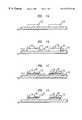
- FIGS. 1A-1Dillustrate the process of the invention.
- FIG. 2is an optical micrograph of a patterned nanotube film fabricated according to the invention.
- FIGS. 3A and 3Breflect Raman spectroscopy data indicating the patterned nature of nanotube films fabricated according to the invention.
- the inventionprovides a process for fabricating patterned, adherent carbon nanotube films.
- One embodiment of the processis shown in FIGS. 1A-1D.
- Related discussion of adherent nanotube filmscan be found in U.S. patent application Ser. No. 09/296,572 (our reference Bower 1-1-37), the disclosure of which is hereby incorporated by reference.
- a flat substrate 10is first provided.
- the substrate 10should be substantially non-reactive with carbon, e.g., not carbide-forming or carbon-dissolving, and should also have a relatively high melting point, typically at least 1000° C.
- Examplesinclude SiO 2 (including Si wafers having an oxidized surface layer), indium tin oxide (ITO), Al 2 O 3 , Cu, and Pt.
- a material 12is deposited onto the substrate 10 in a pattern desired for the nanotube film.
- the patterning material 12is selected from (a) carbon-dissolving materials, (b) carbide-forming materials, and (c) low melting point (about 700° C. or less) metals.
- Carbon-dissolving materialsare known in the art, as reflected, for example in T. B. Massalski, Binary Alloy Phase Diagrams, Vol. I, ASM International, and include elements such as Ni, Fe, Co, and Mn.
- Carbide-forming elementsare similarly known in the art, as reflected in Massalski, supra, and include elements such as Si, Mo, Ti, Ta, W, Nb, Zr, V, Cr, and Hf.
- Typical low melting point metalsinclude Al, Sn, Cd, Zn, and Bi.
- the thickness of the patterning material 12is typically 10 to 100 nm.
- the patterning materialis deposited by any suitable technique, e.g., sputtering, evaporation, or chemical vapor deposition. Conventional lithographic processes are generally used to provide the desired pattern.
- Carbon nanotubes 14are then deposited onto the patterned substrate 10 , as reflected in FIG. 1 B.
- the nanotubesare typically deposited by suspension casting or spray coating.
- Suspension castingis generally performed by placing the substrate into a nanotube suspension made up of nanotubes and a solvent such as methanol, and allowing the solvent to evaporate.
- Spray coatingis performed by spraying such a suspension onto the substrate (which is typically heated) using an air gun, and allowing the solvent to evaporate. Both methods tend to provide relatively uniform thin films of randomly oriented nanotubes.
- the substrate 10is then annealed, generally in vacuum (10 ⁇ 6 torr or less).
- the temperature of the annealis selected based on the patterning material 12 . Specifically, the temperature is chosen to promote carbon dissolution, carbide formation, or melting of the patterning material 12 .
- the annealis generally performed 30 minutes to 24 hours, depending on the particular patterning material. By inducing carbon dissolution, carbide formation or melting at the areas where the nanotubes 14 contact the patterning material 12 , an area 16 of enhanced adherence between the nanotubes 14 and patterning material 12 is created.
- a carbideis formed by reaction of the material and at least a portion of the nanotubes.
- a metal-carbon solid solutionis formed by reaction of the material and at least a portion of the nanotubes. And for low melting point metals, at least a portion of the nanotubes become physically embedded in a molten metal layer and then held in place upon cooling. reflected in FIG. 1D, the nanotubes deposited directly on the substrate 10 material are removed after annealing. Because the nanotubes have relatively poor adherence to the substrate 10 material, removal is relatively easy. Removal is capable of being performed by blowing, rubbing, or brushing the surface of the substrate 10 , or by ultrasonication in a solvent such as methanol. It is possible to combine these techniques. Typically, the substrate is ultrasonicated without blowing, rubbing, or brushing. Ultrasonication, when performed without any other removal technique, is generally performed for 0.5 to 24 hours.
- the thickness of the resultant adherent, patterned nanotube filmis generally 100 to 1000 nm.
- the adhesion strength of the resultant patterned nanotube filmsis sufficient to exceed the 2 A or 2 B scale in the ASTM tape test D3359-97.
- the patterned nanotube filmsare useful in a variety of applications, including vacuum microelectronic devices such as flat panel displays, as well as novel applications such as interconnects in silicon-based devices.
- a silicon substrate with an oxidized surfacewas provided.
- Al pads having an area of 100 ⁇ 70 ⁇ m and a thickness of 50 nmwere patterned onto the substrate surface by thermal evaporation, using a shadow mask.
- Single wall carbon nanotubeswere obtained.
- the nanotubeshad been fabricated by laser ablation with bundle diameters of 10 to 30 nm and lengths of 2 to 10 ⁇ m, and were then purified using an ultrasonically assisted filtration technique (see, e.g., K. B. Shelimov et al., “Purification of Single Wall Nanotubes by Ultrasonically Assisted Filtration,” Chem. Phys. Lett., Vol. 282, p. 429 (1998)).
- the nanotubeswere deposited onto the patterned substrate by spraying.
- the substratewas then vacuum annealed at 700° C. for 30 minutes (the melting point of Al is about 660° C.), and ultrasonicated in for two hours.
- the resulting patterned nanotube filmis shown in FIG. 2, with coated pads 20 , and uncoated substrate surface 22 .
- a silicon substrate with an oxidized surfacewas provided.
- Fe pads having an area of 70 ⁇ 70 ⁇ m and a thickness of 20 nmwere patterned onto the substrate surface by sputtering, using a shadow mask.
- Single wall carbon nanotubeswere obtained as in Example 1.
- the nanotubeswere deposited onto the patterned substrate by spraying.
- the substratewas then vacuum annealed at 800° C. for 30 minutes, and ultrasonicated in methanol for 2 hours.
Landscapes
- Chemical & Material Sciences (AREA)
- Engineering & Computer Science (AREA)
- Nanotechnology (AREA)
- Materials Engineering (AREA)
- Crystallography & Structural Chemistry (AREA)
- Organic Chemistry (AREA)
- Manufacturing & Machinery (AREA)
- Physics & Mathematics (AREA)
- Condensed Matter Physics & Semiconductors (AREA)
- General Physics & Mathematics (AREA)
- Inorganic Chemistry (AREA)
- Composite Materials (AREA)
- Carbon And Carbon Compounds (AREA)
- Other Surface Treatments For Metallic Materials (AREA)
- Cold Cathode And The Manufacture (AREA)
Abstract
Description
Claims (9)
Priority Applications (6)
| Application Number | Priority Date | Filing Date | Title |
|---|---|---|---|
| US09/376,457US6277318B1 (en) | 1999-08-18 | 1999-08-18 | Method for fabrication of patterned carbon nanotube films |
| CA002315132ACA2315132C (en) | 1999-08-18 | 2000-08-04 | Method for fabrication of patterned carbon nanotube films |
| EP00306690AEP1096533B1 (en) | 1999-08-18 | 2000-08-07 | Method for fabrication of patterned carbon nanotube films |
| DE60026240TDE60026240T2 (en) | 1999-08-18 | 2000-08-07 | Manufacturing method of a patterned carbon nanotube layer |
| JP2000247135AJP3442039B2 (en) | 1999-08-18 | 2000-08-17 | Fabrication method of patterned carbon nanotube thin film |
| KR1020000047469AKR100730496B1 (en) | 1999-08-18 | 2000-08-17 | Method for fabrication of patterned carbon nanotube films |
Applications Claiming Priority (1)
| Application Number | Priority Date | Filing Date | Title |
|---|---|---|---|
| US09/376,457US6277318B1 (en) | 1999-08-18 | 1999-08-18 | Method for fabrication of patterned carbon nanotube films |
Publications (1)
| Publication Number | Publication Date |
|---|---|
| US6277318B1true US6277318B1 (en) | 2001-08-21 |
Family
ID=23485110
Family Applications (1)
| Application Number | Title | Priority Date | Filing Date |
|---|---|---|---|
| US09/376,457Expired - LifetimeUS6277318B1 (en) | 1999-08-18 | 1999-08-18 | Method for fabrication of patterned carbon nanotube films |
Country Status (6)
| Country | Link |
|---|---|
| US (1) | US6277318B1 (en) |
| EP (1) | EP1096533B1 (en) |
| JP (1) | JP3442039B2 (en) |
| KR (1) | KR100730496B1 (en) |
| CA (1) | CA2315132C (en) |
| DE (1) | DE60026240T2 (en) |
Cited By (190)
| Publication number | Priority date | Publication date | Assignee | Title |
|---|---|---|---|---|
| US20010004471A1 (en)* | 1999-12-17 | 2001-06-21 | Nec Corporation | Method of processing a nanotube |
| US20020074932A1 (en)* | 2000-06-21 | 2002-06-20 | Bouchard Robert Joseph | Process for improving the emission of electron field emitters |
| US6420092B1 (en)* | 1999-07-14 | 2002-07-16 | Cheng-Jer Yang | Low dielectric constant nanotube |
| US6422450B1 (en)* | 1999-03-01 | 2002-07-23 | University Of North Carolina, The Chapel | Nanotube-based high energy material and method |
| US6436221B1 (en)* | 2001-02-07 | 2002-08-20 | Industrial Technology Research Institute | Method of improving field emission efficiency for fabricating carbon nanotube field emitters |
| US20020140336A1 (en)* | 2001-03-27 | 2002-10-03 | Stoner Brian R. | Coated electrode with enhanced electron emission and ignition characteristics |
| US20030001141A1 (en)* | 2001-04-26 | 2003-01-02 | Yi Sun | Method for dissolving nanostructural materials |
| US6504292B1 (en)* | 1999-07-15 | 2003-01-07 | Agere Systems Inc. | Field emitting device comprising metallized nanostructures and method for making the same |
| US20030021966A1 (en)* | 2001-07-25 | 2003-01-30 | Segal Brent M. | Electromechanical memory array using nanotube ribbons and method for making same |
| US20030046809A1 (en)* | 2001-09-11 | 2003-03-13 | Egon Mergenthaler | Method of connecting a device to a support, and pad for establishing a connection between a device and a support |
| US6544463B1 (en)* | 1999-07-26 | 2003-04-08 | The Trustees Of The University Of Pennsylvania | Hybrid materials and methods for producing the same |
| US20030092207A1 (en)* | 2001-10-19 | 2003-05-15 | Zvi Yaniv | Activation effect on carbon nanotubes |
| US20030121887A1 (en)* | 2001-03-22 | 2003-07-03 | Garvey James F. | Multi-component substances and processes for preparation thereof |
| DE10161312A1 (en)* | 2001-12-13 | 2003-07-10 | Infineon Technologies Ag | Method for producing a layer arrangement and layer arrangement |
| US6605894B2 (en)* | 2000-12-05 | 2003-08-12 | Electronics And Telecommunications Research Institute | Field emission devices using carbon nanotubes and method thereof |
| US6613198B2 (en) | 2001-04-18 | 2003-09-02 | James F. Garvey | Pulsed arc molecular beam process |
| US20030180472A1 (en)* | 2002-03-25 | 2003-09-25 | Otto Zhou | Method for assembling nano objects |
| US6630772B1 (en)* | 1998-09-21 | 2003-10-07 | Agere Systems Inc. | Device comprising carbon nanotube field emitter structure and process for forming device |
| US20030211029A1 (en)* | 2002-03-25 | 2003-11-13 | Mitsubishi Gas Chemical Company, Inc. | Aligned carbon nanotube films and a process for producing them |
| US20040011291A1 (en)* | 2000-10-27 | 2004-01-22 | Marc Delaunay | Electron cyclotron resonance plasma deposition process and device for single-wall carbon nanotubes and nanotubes thus obtained |
| US20040028183A1 (en)* | 2000-10-06 | 2004-02-12 | Jianping Lu | Method and apparatus for controlling electron beam current |
| US6706402B2 (en) | 2001-07-25 | 2004-03-16 | Nantero, Inc. | Nanotube films and articles |
| US20040055892A1 (en)* | 2001-11-30 | 2004-03-25 | University Of North Carolina At Chapel Hill | Deposition method for nanostructure materials |
| US20040101468A1 (en)* | 2002-11-21 | 2004-05-27 | Liang Liu | Carbon nanotube array and method for forming same |
| US20040101469A1 (en)* | 2002-08-09 | 2004-05-27 | Nanolnk, Inc. | Apparatus, materials, and methods for fabrication and catalysis |
| US20040114721A1 (en)* | 2000-10-06 | 2004-06-17 | Applied Nanotechnologies, Inc. | Devices and methods for producing multiple x-ray beams from multiple locations |
| US20040136896A1 (en)* | 2002-12-21 | 2004-07-15 | Liang Liu | Carbon annotate-based device and method for making carbon nanotube based device |
| WO2004065657A1 (en)* | 2003-01-13 | 2004-08-05 | Nantero, Inc. | Methods of making carbon nanotube films, layers, fabrics, ribbons, elements and articles |
| US6784028B2 (en) | 2001-12-28 | 2004-08-31 | Nantero, Inc. | Methods of making electromechanical three-trace junction devices |
| US20040169281A1 (en)* | 2003-02-27 | 2004-09-02 | Applied Materials, Inc. | Ultra low k plasma CVD nanotube/spin-on dielectrics with improved properties for advanced nanoelectronic device fabrication |
| US20040174110A1 (en)* | 2001-06-18 | 2004-09-09 | Fuminori Ito | Field emission type cold cathode and method of manufacturing the cold cathode |
| US20040173378A1 (en)* | 2002-12-09 | 2004-09-09 | University Of North Carolina At Chapel Hill | Methods for assembly and sorting of nanostructure-containing materials and related articles |
| US20040184981A1 (en)* | 2003-03-19 | 2004-09-23 | Liang Liu | Carbon nanotube array and method for forming same |
| US6812635B2 (en) | 2001-12-28 | 2004-11-02 | Electronics And Telecommunications Research Institute | Cathode for field emission device |
| US20040233147A1 (en)* | 2003-05-20 | 2004-11-25 | Genshiro Kawachi | Light emission type display apparatus |
| US20040241896A1 (en)* | 2003-03-21 | 2004-12-02 | The University Of North Carolina At Chapel Hill | Methods and apparatus for patterned deposition of nanostructure-containing materials by self-assembly and related articles |
| US6836424B2 (en) | 2001-07-25 | 2004-12-28 | Nantero, Inc. | Hybrid circuit having nanotube electromechanical memory |
| US6835591B2 (en) | 2001-07-25 | 2004-12-28 | Nantero, Inc. | Methods of nanotube films and articles |
| US6850595B2 (en) | 2000-10-06 | 2005-02-01 | The University Of North Carolina At Chapel Hill | X-ray generating mechanism using electron field emission cathode |
| US20050026531A1 (en)* | 2003-07-31 | 2005-02-03 | Semiconductor Energy Laboratory Co., Ltd. | Method for manufacturing ultrafine carbon fiber and field emission element |
| US20050034668A1 (en)* | 2001-03-22 | 2005-02-17 | Garvey James F. | Multi-component substances and apparatus for preparation thereof |
| US6858197B1 (en) | 2002-03-13 | 2005-02-22 | The United States Of America As Represented By The Administrator Of The National Aeronautics And Space Administration | Controlled patterning and growth of single wall and multi-wall carbon nanotubes |
| US20050058590A1 (en)* | 2003-09-08 | 2005-03-17 | Nantero, Inc. | Spin-coatable liquid for formation of high purity nanotube films |
| US20050065741A1 (en)* | 2003-05-14 | 2005-03-24 | Nantero, Inc. | Sensor platform using a non-horizontally oriented nanotube element |
| US6876724B2 (en) | 2000-10-06 | 2005-04-05 | The University Of North Carolina - Chapel Hill | Large-area individually addressable multi-beam x-ray system and method of forming same |
| US6911682B2 (en) | 2001-12-28 | 2005-06-28 | Nantero, Inc. | Electromechanical three-trace junction devices |
| US20050164583A1 (en)* | 1999-11-26 | 2005-07-28 | Geohegan David B. | Condensed phase conversion and growth of nanorods and other materials instead of from vapor |
| US20050176336A1 (en)* | 2004-02-05 | 2005-08-11 | Lee Sang-Hyun | Method of manufacturing field emitter |
| US20050214195A1 (en)* | 2004-03-27 | 2005-09-29 | Jung Hee T | Method for manufacturing a carbon nanotube multilayer pattern using photolithography and dry etching |
| US20050226361A1 (en)* | 2000-10-06 | 2005-10-13 | The University Of North Carolina At Chapel Hill | Computed tomography scanning system and method using a field emission x-ray source |
| US20050231091A1 (en)* | 2001-06-15 | 2005-10-20 | Bouchard Robert J | Process for improving the emission of electron field emitters |
| US20050238810A1 (en)* | 2004-04-26 | 2005-10-27 | Mainstream Engineering Corp. | Nanotube/metal substrate composites and methods for producing such composites |
| US6967013B2 (en) | 2001-03-14 | 2005-11-22 | Mitsubishi Gas Chemical Company, Inc. | Process for producing aligned carbon nanotube films |
| US20050269554A1 (en)* | 2004-06-03 | 2005-12-08 | Nantero, Inc. | Applicator liquid containing ethyl lactate for preparation of nanotube films |
| US20050269553A1 (en)* | 2003-09-08 | 2005-12-08 | Nantero, Inc. | Spin-coatable liquid for use in electronic fabrication processes |
| US20050271808A1 (en)* | 2004-03-25 | 2005-12-08 | Nomadics, Inc. | Process and apparatus for layer by layer assembly of reinforced composite materials |
| US20050269559A1 (en)* | 2004-06-02 | 2005-12-08 | Xintek, Inc. | Field emission ion source based on nanostructure-containing material |
| US20060008047A1 (en)* | 2000-10-06 | 2006-01-12 | The University Of North Carolina At Chapel Hill | Computed tomography system for imaging of human and small animal |
| US20060055303A1 (en)* | 2003-12-24 | 2006-03-16 | Jie Liu | Method of synthesizing small-diameter carbon nanotubes with electron field emission properties |
| US20060096950A1 (en)* | 2003-12-18 | 2006-05-11 | Nano-Proprietary, Inc. | Bead blast activation of carbon nanotube cathode |
| US20060123628A1 (en)* | 2002-02-05 | 2006-06-15 | Fuji Xerox Co., Ltd. | Method of manufacturing a carbon nanotube device |
| US7067237B2 (en) | 2003-06-28 | 2006-06-27 | Samsung Electronics Co., Ltd. | Method for forming pattern of one-dimensional nanostructure |
| US20060181854A1 (en)* | 2002-04-23 | 2006-08-17 | Freedman Philip D | Patterned structure, method of making and use |
| US20060193093A1 (en)* | 2004-11-02 | 2006-08-31 | Nantero, Inc. | Nanotube ESD protective devices and corresponding nonvolatile and volatile nanotube switches |
| US7120047B2 (en) | 2001-07-25 | 2006-10-10 | Segal Brent M | Device selection circuitry constructed with nanotube technology |
| US20060260785A1 (en)* | 2005-05-13 | 2006-11-23 | Delta Electronics, Inc. | Heat sink |
| US20060281256A1 (en)* | 2005-06-08 | 2006-12-14 | Carter Richard J | Self-aligned cell integration scheme |
| US7157848B2 (en) | 2003-06-06 | 2007-01-02 | Electrovac Fabrikation Elektrotechnischer Spezialartikel Gmbh | Field emission backlight for liquid crystal television |
| US20070004191A1 (en)* | 2005-06-30 | 2007-01-04 | Lsi Logic Corporation | Novel techniques for precision pattern transfer of carbon nanotubes from photo mask to wafers |
| US20070014148A1 (en)* | 2004-05-10 | 2007-01-18 | The University Of North Carolina At Chapel Hill | Methods and systems for attaching a magnetic nanowire to an object and apparatuses formed therefrom |
| US7176505B2 (en) | 2001-12-28 | 2007-02-13 | Nantero, Inc. | Electromechanical three-trace junction devices |
| US20070053489A1 (en)* | 2005-04-25 | 2007-03-08 | The University Of North Carolina At Chapel Hill | X-ray imaging systems and methods using temporal digital signal processing for reducing noise and for obtaining multiple images simultaneously |
| RU2296046C1 (en)* | 2005-10-25 | 2007-03-27 | Институт физики твердого тела РАН | Method of treatment of the carbonic nanotubes |
| US7202596B2 (en) | 2003-06-06 | 2007-04-10 | Electrovac Ag | Electron emitter and process of fabrication |
| US7220971B1 (en) | 2004-12-29 | 2007-05-22 | The University Of North Carolina At Chapel Hill | Multi-pixel electron microbeam irradiator systems and methods for selectively irradiating predetermined locations |
| US20070144431A1 (en)* | 2005-10-14 | 2007-06-28 | Hon Hai Precision Industry Co., Ltd. | Apparatus for forming carbon nanotube film |
| US20070158768A1 (en)* | 2006-01-06 | 2007-07-12 | Honeywell International, Inc. | Electrical contacts formed of carbon nanotubes |
| US7252749B2 (en) | 2001-11-30 | 2007-08-07 | The University Of North Carolina At Chapel Hill | Deposition method for nanostructure materials |
| US7274078B2 (en) | 2001-07-25 | 2007-09-25 | Nantero, Inc. | Devices having vertically-disposed nanofabric articles and methods of making the same |
| US20070222353A1 (en)* | 2004-07-16 | 2007-09-27 | The Trustees Of Boston College | Device and method for achieving enhanced field emission utilizing nanostructures grown on a conductive substrate |
| US20070243717A1 (en)* | 2004-11-29 | 2007-10-18 | Francisco Santiago | Carbon nanotube apparatus and method of carbon nanotube modification |
| US7304357B2 (en) | 2001-07-25 | 2007-12-04 | Nantero, Inc. | Devices having horizontally-disposed nanofabric articles and methods of making the same |
| US20070278925A1 (en)* | 2004-09-10 | 2007-12-06 | Nano-Proprietary, Inc. | Enhanced electron field emission from carbon nanotubes without activation |
| US20070292622A1 (en)* | 2005-08-04 | 2007-12-20 | Rowley Lawrence A | Solvent containing carbon nanotube aqueous dispersions |
| US20080012461A1 (en)* | 2004-11-09 | 2008-01-17 | Nano-Proprietary, Inc. | Carbon nanotube cold cathode |
| US7335395B2 (en)* | 2002-04-23 | 2008-02-26 | Nantero, Inc. | Methods of using pre-formed nanotubes to make carbon nanotube films, layers, fabrics, ribbons, elements and articles |
| US20080069420A1 (en)* | 2006-05-19 | 2008-03-20 | Jian Zhang | Methods, systems, and computer porgram products for binary multiplexing x-ray radiography |
| US20080079027A1 (en)* | 2004-06-09 | 2008-04-03 | Nantero, Inc. | Field effect devices having a gate controlled via a nanotube switching element |
| RU2321536C1 (en)* | 2006-07-05 | 2008-04-10 | Институт физики твердого тела РАН | Device for increase of sorption ability of carbon nanotubes |
| US20080111110A1 (en)* | 2002-06-14 | 2008-05-15 | Hyperion Catalysis International, Inc. | Electroconductive Carbon Fibril-based Inks and Coatings |
| US20080131705A1 (en)* | 2006-12-01 | 2008-06-05 | International Business Machines Corporation | Method and system for nanostructure placement using imprint lithography |
| US20080142850A1 (en)* | 2005-05-09 | 2008-06-19 | Nantero, Inc. | Memory elements and cross point switches and arrays of same using nonvolatile nanotube blocks |
| US20080157257A1 (en)* | 2005-05-09 | 2008-07-03 | Nantero, Inc. | Nonvolatile nanotube diodes and nonvolatile nanotube blocks and systems using same and methods of making same |
| US20080157127A1 (en)* | 2005-05-09 | 2008-07-03 | Nantero, Inc. | Nonvolatile nanotube diodes and nonvolatile nanotube blocks and systems using same and methods of making same |
| US20080157126A1 (en)* | 2005-05-09 | 2008-07-03 | Nantero, Inc. | Nonvolatile nanotube diodes and nonvolatile nanotube blocks and systems using same and methods of making same |
| KR100844504B1 (en) | 2007-03-14 | 2008-07-08 | 한국표준과학연구원 | How to control the direction of carbon nanotubes by applying direct friction from the outside |
| US20080170429A1 (en)* | 2005-05-09 | 2008-07-17 | Nantero, Inc. | Nonvolatile nanotube diodes and nonvolatile nanotube blocks and systems using same and methods of making same |
| US20080212361A1 (en)* | 2005-05-09 | 2008-09-04 | Nantero, Inc. | Nonvolatile nanotube diodes and nonvolatile nanotube blocks and systems using same and methods of making same |
| US20080231413A1 (en)* | 2004-09-21 | 2008-09-25 | Nantero, Inc. | Resistive elements using carbon nanotubes |
| US20080238882A1 (en)* | 2007-02-21 | 2008-10-02 | Ramesh Sivarajan | Symmetric touch screen system with carbon nanotube-based transparent conductive electrode pairs |
| US20080251877A1 (en)* | 2007-04-12 | 2008-10-16 | Kanti Jain | Methods for fabricating complex micro and nanoscale structures and electronic devices and components made by the same |
| US20080280038A1 (en)* | 2003-01-13 | 2008-11-13 | Nantero, Inc. | Methods of using thin metal layers to make carbon nanotube films, layers, fabrics, ribbons, elements and articles |
| US20080292899A1 (en)* | 2005-09-07 | 2008-11-27 | E&F Corporation | Titanium Alloy Composite Material, Method of Producing the Titanium Alloy Composite Material, Titanium Clad Material Using the Titanium Alloy Composite Material, and Method of Producing the Titanium Clad Material |
| US20090023098A1 (en)* | 2007-07-16 | 2009-01-22 | Kanti Jain | Method for fabricating dual damascene profiles using sub pixel-voting lithography and devices made by same |
| US20090051032A1 (en)* | 2003-09-08 | 2009-02-26 | Segal Brent M | Patterned nanoscopic articles and methods of making the same |
| US20090061161A1 (en)* | 2007-08-27 | 2009-03-05 | Lynn Sheehan | Laser patterning of a cross-linked polymer |
| US20090086923A1 (en)* | 2007-09-28 | 2009-04-02 | Davis Robert C | X-ray radiation window with carbon nanotube frame |
| US20090099016A1 (en)* | 2005-12-19 | 2009-04-16 | Advanced Technology Materials, Inc. | Production of carbon nanotubes |
| US20090115305A1 (en)* | 2007-05-22 | 2009-05-07 | Nantero, Inc. | Triodes using nanofabric articles and methods of making the same |
| US20090140167A1 (en)* | 2005-09-06 | 2009-06-04 | Natero, Inc. | Nanotube fabric-based sensor systems and methods of making same |
| US7556746B2 (en) | 2004-06-03 | 2009-07-07 | Nantero, Inc. | Method of making an applicator liquid for electronics fabrication process |
| US20090173964A1 (en)* | 2001-07-25 | 2009-07-09 | Nantero, Inc. | Method of forming a carbon nanotube-based contact to semiconductor |
| US7560136B2 (en) | 2003-01-13 | 2009-07-14 | Nantero, Inc. | Methods of using thin metal layers to make carbon nanotube films, layers, fabrics, ribbons, elements and articles |
| US20090184389A1 (en)* | 2005-05-09 | 2009-07-23 | Bertin Claude L | Nonvolatile Nanotube Diodes and Nonvolatile Nanotube Blocks and Systems Using Same and Methods of Making Same |
| US7566478B2 (en) | 2001-07-25 | 2009-07-28 | Nantero, Inc. | Methods of making carbon nanotube films, layers, fabrics, ribbons, elements and articles |
| US20090194839A1 (en)* | 2005-11-15 | 2009-08-06 | Bertin Claude L | Nonvolatile nanotube diodes and nonvolatile nanotube blocks and systems using same and methods of making same |
| US20090202644A1 (en)* | 2005-04-06 | 2009-08-13 | Drexel University | Functional nanoparticle filled carbon nanotubes and methods of their production |
| EP2096659A1 (en) | 2008-02-29 | 2009-09-02 | Korea University Industry & Academy Cooperation Foundation | Electron emission source, electric device using the same, and method of manufacturing the electron emission source |
| US20090239042A1 (en)* | 2008-03-21 | 2009-09-24 | Kanti Jain | Material Assisted Laser Ablation |
| US7598127B2 (en) | 2005-05-12 | 2009-10-06 | Nantero, Inc. | Nanotube fuse structure |
| US20090311489A1 (en)* | 2007-08-27 | 2009-12-17 | Lynn Sheehan | Laser patterning of a carbon nanotube layer |
| US20100001267A1 (en)* | 2008-06-20 | 2010-01-07 | Nantero, Inc. | Nram arrays with nanotube blocks, nanotube traces, and nanotube planes and methods of making same |
| RU2379228C1 (en)* | 2008-09-24 | 2010-01-20 | Учреждение Российской академии наук Институт физики твердого тела РАН | Method of filling carbon nanotubes with hydrogen |
| US7666382B2 (en) | 2004-12-16 | 2010-02-23 | Nantero, Inc. | Aqueous carbon nanotube applicator liquids and methods for producing applicator liquids thereof |
| US7704547B1 (en) | 2004-12-07 | 2010-04-27 | The United States Of America As Represented By The Administrator Of The National Aeronautics And Space Administration (Nasa) | Carbon nanotube growth density control |
| US7718223B1 (en)* | 2004-12-07 | 2010-05-18 | The United States Of America As Represented By The Administrator Of The National Aeronautics And Space Administration (Nasa) | Control of carbon nanotube density and tower height in an array |
| US20100129654A1 (en)* | 2005-12-16 | 2010-05-27 | Tsinghua University | Carbon nanotube yarn and method for making the same |
| US20100143848A1 (en)* | 2008-12-09 | 2010-06-10 | Kanti Jain | Patterning methods for stretchable structures |
| US20100147657A1 (en)* | 2004-11-02 | 2010-06-17 | Nantero, Inc. | Nanotube esd protective devices and corresponding nonvolatile and volatile nanotube switches |
| US7781862B2 (en) | 2005-05-09 | 2010-08-24 | Nantero, Inc. | Two-terminal nanotube devices and systems and methods of making same |
| US20100239064A1 (en)* | 2005-04-25 | 2010-09-23 | Unc-Chapel Hill | Methods, systems, and computer program products for multiplexing computed tomography |
| US20100267205A1 (en)* | 2005-09-06 | 2010-10-21 | Lockheed Martin Corporation | Carbon nanotubes for the selective transfer of heat from electronics |
| US7858185B2 (en) | 2003-09-08 | 2010-12-28 | Nantero, Inc. | High purity nanotube fabrics and films |
| US20100327247A1 (en)* | 2005-09-06 | 2010-12-30 | Nantero, Inc. | Method and system of using nanotube fabrics as joule heating elements for memories and other applications |
| US20100329413A1 (en)* | 2009-01-16 | 2010-12-30 | Zhou Otto Z | Compact microbeam radiation therapy systems and methods for cancer treatment and research |
| US20110027497A1 (en)* | 2009-07-31 | 2011-02-03 | Nantero, Inc. | Anisotropic nanotube fabric layers and films and methods of forming same |
| US20110034008A1 (en)* | 2009-08-07 | 2011-02-10 | Nantero, Inc. | Method for forming a textured surface on a semiconductor substrate using a nanofabric layer |
| US7915637B2 (en) | 2008-11-19 | 2011-03-29 | Nantero, Inc. | Switching materials comprising mixed nanoscopic particles and carbon nanotubes and method of making and using the same |
| US20110136662A1 (en)* | 2009-12-04 | 2011-06-09 | Chen C C | Catalytic seeding control method |
| US20110147715A1 (en)* | 2008-06-16 | 2011-06-23 | Purdue Research Foundation | Medium Scale Carbon Nanotube Thin Film Integrated Circuits on Flexible Plastic Substrates |
| US20110156009A1 (en)* | 2009-12-31 | 2011-06-30 | Manning H Montgomery | Compact electrical switching devices with nanotube elements, and methods of making same |
| US20110163290A1 (en)* | 2009-10-23 | 2011-07-07 | Nantero, Inc. | Methods for passivating a carbonic nanolayer |
| US7983394B2 (en) | 2009-12-17 | 2011-07-19 | Moxtek, Inc. | Multiple wavelength X-ray source |
| US20110203632A1 (en)* | 2010-02-22 | 2011-08-25 | Rahul Sen | Photovoltaic devices using semiconducting nanotube layers |
| US8110883B2 (en) | 2007-03-12 | 2012-02-07 | Nantero Inc. | Electromagnetic and thermal sensors using carbon nanotubes and methods of making same |
| US8247971B1 (en) | 2009-03-19 | 2012-08-21 | Moxtek, Inc. | Resistively heated small planar filament |
| US8351239B2 (en) | 2009-10-23 | 2013-01-08 | Nantero Inc. | Dynamic sense current supply circuit and associated method for reading and characterizing a resistive memory array |
| US8358739B2 (en) | 2010-09-03 | 2013-01-22 | The University Of North Carolina At Chapel Hill | Systems and methods for temporal multiplexing X-ray imaging |
| US8420978B2 (en) | 2007-01-18 | 2013-04-16 | The Board Of Trustees Of The University Of Illinois | High throughput, low cost dual-mode patterning method for large area substrates |
| US8471238B2 (en) | 2004-09-16 | 2013-06-25 | Nantero Inc. | Light emitters using nanotubes and methods of making same |
| US8498381B2 (en) | 2010-10-07 | 2013-07-30 | Moxtek, Inc. | Polymer layer on X-ray window |
| US8526574B2 (en) | 2010-09-24 | 2013-09-03 | Moxtek, Inc. | Capacitor AC power coupling across high DC voltage differential |
| US8574673B2 (en) | 2009-07-31 | 2013-11-05 | Nantero Inc. | Anisotropic nanotube fabric layers and films and methods of forming same |
| US8580586B2 (en) | 2005-05-09 | 2013-11-12 | Nantero Inc. | Memory arrays using nanotube articles with reprogrammable resistance |
| US8736138B2 (en) | 2007-09-28 | 2014-05-27 | Brigham Young University | Carbon nanotube MEMS assembly |
| US8750458B1 (en) | 2011-02-17 | 2014-06-10 | Moxtek, Inc. | Cold electron number amplifier |
| US8761344B2 (en) | 2011-12-29 | 2014-06-24 | Moxtek, Inc. | Small x-ray tube with electron beam control optics |
| US8792619B2 (en) | 2011-03-30 | 2014-07-29 | Moxtek, Inc. | X-ray tube with semiconductor coating |
| US8804910B1 (en) | 2011-01-24 | 2014-08-12 | Moxtek, Inc. | Reduced power consumption X-ray source |
| US8809230B2 (en) | 2010-08-02 | 2014-08-19 | Lawrence Livermore National Security, Llc | Porous substrates filled with nanomaterials |
| US8817950B2 (en) | 2011-12-22 | 2014-08-26 | Moxtek, Inc. | X-ray tube to power supply connector |
| US8895950B2 (en) | 2009-10-23 | 2014-11-25 | Nantero Inc. | Methods for passivating a carbonic nanolayer |
| US8929515B2 (en) | 2011-02-23 | 2015-01-06 | Moxtek, Inc. | Multiple-size support for X-ray window |
| US8937575B2 (en) | 2009-07-31 | 2015-01-20 | Nantero Inc. | Microstrip antenna elements and arrays comprising a shaped nanotube fabric layer and integrated two terminal nanotube select devices |
| US8941094B2 (en) | 2010-09-02 | 2015-01-27 | Nantero Inc. | Methods for adjusting the conductivity range of a nanotube fabric layer |
| US8995621B2 (en) | 2010-09-24 | 2015-03-31 | Moxtek, Inc. | Compact X-ray source |
| US9053890B2 (en) | 2013-08-02 | 2015-06-09 | University Health Network | Nanostructure field emission cathode structure and method for making |
| US9173623B2 (en) | 2013-04-19 | 2015-11-03 | Samuel Soonho Lee | X-ray tube and receiver inside mouth |
| US9299430B1 (en) | 2015-01-22 | 2016-03-29 | Nantero Inc. | Methods for reading and programming 1-R resistive change element arrays |
| US9305735B2 (en) | 2007-09-28 | 2016-04-05 | Brigham Young University | Reinforced polymer x-ray window |
| US9422651B2 (en) | 2003-01-13 | 2016-08-23 | Nantero Inc. | Methods for arranging nanoscopic elements within networks, fabrics, and films |
| US9574290B2 (en) | 2003-01-13 | 2017-02-21 | Nantero Inc. | Methods for arranging nanotube elements within nanotube fabrics and films |
| CN106463320A (en)* | 2014-02-10 | 2017-02-22 | 勒博特公司 | An electron emitter for an x-ray tube |
| US9617151B2 (en) | 2010-02-12 | 2017-04-11 | Nantero Inc. | Methods for controlling density, porosity, and/or gap size within nanotube fabric layers and films |
| US20170133610A1 (en)* | 2015-11-05 | 2017-05-11 | International Business Machines Corporation | End-bonded metal contacts on carbon nanotubes |
| US9650732B2 (en) | 2013-05-01 | 2017-05-16 | Nantero Inc. | Low defect nanotube application solutions and fabrics and methods for making same |
| US20170244040A1 (en)* | 2016-02-18 | 2017-08-24 | International Business Machines Corporation | Formation of carbon nanotube-containing devices |
| US9911743B2 (en) | 2005-05-09 | 2018-03-06 | Nantero, Inc. | Nonvolatile nanotube diodes and nonvolatile nanotube blocks and systems using same and methods of making same |
| US9934848B2 (en) | 2016-06-07 | 2018-04-03 | Nantero, Inc. | Methods for determining the resistive states of resistive change elements |
| US9941001B2 (en) | 2016-06-07 | 2018-04-10 | Nantero, Inc. | Circuits for determining the resistive states of resistive change elements |
| WO2019191801A1 (en) | 2018-04-06 | 2019-10-10 | Micro-X Limited | Large scale stable field emitter for high current applications |
| US10654718B2 (en) | 2013-09-20 | 2020-05-19 | Nantero, Inc. | Scalable nanotube fabrics and methods for making same |
| US10661304B2 (en) | 2010-03-30 | 2020-05-26 | Nantero, Inc. | Microfluidic control surfaces using ordered nanotube fabrics |
| US10835199B2 (en) | 2016-02-01 | 2020-11-17 | The University Of North Carolina At Chapel Hill | Optical geometry calibration devices, systems, and related methods for three dimensional x-ray imaging |
| US10980494B2 (en) | 2014-10-20 | 2021-04-20 | The University Of North Carolina At Chapel Hill | Systems and related methods for stationary digital chest tomosynthesis (s-DCT) imaging |
| US11570878B2 (en) | 2017-05-25 | 2023-01-31 | Micro-X Limited | Device for producing radio frequency modulated X-ray radiation |
| US11576249B2 (en) | 2018-05-25 | 2023-02-07 | Micro-X Limited | Device for applying beamforming signal processing to RF modulated X-rays |
| US11778717B2 (en) | 2020-06-30 | 2023-10-03 | VEC Imaging GmbH & Co. KG | X-ray source with multiple grids |
| CN117344282A (en)* | 2023-10-09 | 2024-01-05 | 常州六边形纳米科技有限公司 | Method for manufacturing pattern on surface of flexible carbon nano tube film |
| US12230468B2 (en) | 2022-06-30 | 2025-02-18 | Varex Imaging Corporation | X-ray system with field emitters and arc protection |
Families Citing this family (35)
| Publication number | Priority date | Publication date | Assignee | Title |
|---|---|---|---|---|
| KR100372335B1 (en)* | 1999-11-05 | 2003-02-17 | 일진나노텍 주식회사 | Synthesis method for controlling diameter of carbonnanotubes using catalytic metal fine patterns |
| US6297592B1 (en)* | 2000-08-04 | 2001-10-02 | Lucent Technologies Inc. | Microwave vacuum tube device employing grid-modulated cold cathode source having nanotube emitters |
| JP3610325B2 (en) | 2000-09-01 | 2005-01-12 | キヤノン株式会社 | Electron emitting device, electron source, and method of manufacturing image forming apparatus |
| JP3639809B2 (en) | 2000-09-01 | 2005-04-20 | キヤノン株式会社 | ELECTRON EMITTING ELEMENT, ELECTRON EMITTING DEVICE, LIGHT EMITTING DEVICE, AND IMAGE DISPLAY DEVICE |
| JP3658346B2 (en) | 2000-09-01 | 2005-06-08 | キヤノン株式会社 | Electron emitting device, electron source and image forming apparatus, and method for manufacturing electron emitting device |
| JP3639808B2 (en) | 2000-09-01 | 2005-04-20 | キヤノン株式会社 | Electron emitting device, electron source, image forming apparatus, and method of manufacturing electron emitting device |
| JP3634781B2 (en) | 2000-09-22 | 2005-03-30 | キヤノン株式会社 | Electron emission device, electron source, image forming device, and television broadcast display device |
| KR100379620B1 (en)* | 2000-11-21 | 2003-04-10 | 광주과학기술원 | Method of Manufacturing Carbon Nanotube |
| WO2002045113A1 (en)* | 2000-11-29 | 2002-06-06 | Nec Corporation | Pattern forming method for carbon nanotube, and field emission cold cathode and method of manufacturing the cold cathode |
| JP3768908B2 (en) | 2001-03-27 | 2006-04-19 | キヤノン株式会社 | Electron emitting device, electron source, image forming apparatus |
| DE10127351A1 (en)* | 2001-06-06 | 2002-12-19 | Infineon Technologies Ag | Electronic chip comprises several external contacts of which at least two are provided with a plurality of nano-tubes for purposes of contacting an external contact of another electronic chip |
| US6911767B2 (en) | 2001-06-14 | 2005-06-28 | Hyperion Catalysis International, Inc. | Field emission devices using ion bombarded carbon nanotubes |
| CA2450778A1 (en) | 2001-06-14 | 2003-10-16 | Hyperion Catalysis International, Inc. | Field emission devices using modified carbon nanotubes |
| US7341498B2 (en) | 2001-06-14 | 2008-03-11 | Hyperion Catalysis International, Inc. | Method of irradiating field emission cathode having nanotubes |
| KR100407959B1 (en)* | 2001-06-18 | 2003-12-03 | 엘지전자 주식회사 | One-directional aligned carbon nanotube micro string and its fabricating method |
| KR100374042B1 (en)* | 2001-07-11 | 2003-03-03 | 엘지전자 주식회사 | Semiconductor device fabrication method using selective excluding process of carbon nanotube having various characteristics |
| WO2004065671A1 (en)* | 2003-01-13 | 2004-08-05 | Nantero, Inc. | Carbon nanotube films, layers, fabrics, ribbons, elements and articles |
| KR100422217B1 (en)* | 2001-08-02 | 2004-03-12 | 일진나노텍 주식회사 | Method of manufacturing carbon nanotubes-thin film |
| JP3703415B2 (en) | 2001-09-07 | 2005-10-05 | キヤノン株式会社 | ELECTRON EMITTING ELEMENT, ELECTRON SOURCE, IMAGE FORMING APPARATUS, AND METHOD FOR MANUFACTURING ELECTRON EMITTING ELEMENT AND ELECTRON SOURCE |
| JP2003081618A (en)* | 2001-09-07 | 2003-03-19 | Noritake Itron Corp | Method for forming carbon nanotube film |
| JP3605105B2 (en)* | 2001-09-10 | 2004-12-22 | キヤノン株式会社 | Electron emitting element, electron source, light emitting device, image forming apparatus, and method of manufacturing each substrate |
| SE0104452D0 (en)* | 2001-12-28 | 2001-12-28 | Forskarpatent I Vaest Ab | Method for producing nanostructures in-situ, and in-situ prepared nanostructures |
| DE10217362B4 (en)* | 2002-04-18 | 2004-05-13 | Infineon Technologies Ag | Targeted deposition of nanotubes |
| JP3797299B2 (en)* | 2002-08-30 | 2006-07-12 | 石川島播磨重工業株式会社 | High voltage cathode and bonding method thereof |
| TW594824B (en)* | 2002-12-03 | 2004-06-21 | Ind Tech Res Inst | Triode structure of field-emission display and manufacturing method thereof |
| JP4379002B2 (en) | 2003-05-30 | 2009-12-09 | 富士ゼロックス株式会社 | Carbon nanotube device manufacturing method and carbon nanotube transfer body |
| WO2005061382A1 (en)* | 2003-12-24 | 2005-07-07 | Nanometrix Inc. | Continuous production of carbon nanotubes |
| US7713577B2 (en) | 2005-03-01 | 2010-05-11 | Los Alamos National Security, Llc | Preparation of graphitic articles |
| CN101188179B (en)* | 2006-11-15 | 2010-05-26 | 清华大学 | Manufacturing method of field emission electron source |
| KR100875115B1 (en) | 2007-05-10 | 2008-12-22 | 삼성에스디아이 주식회사 | Hybrid composites containing carbon nanotubes and carbide-derived carbon, electron emitters including the hybrid composites and methods for manufacturing the same, and electron emitters employing the electron emitters |
| WO2009016546A2 (en)* | 2007-07-30 | 2009-02-05 | Philips Intellectual Property & Standards Gmbh | Nanostructures and method for making them |
| KR101015309B1 (en)* | 2008-06-27 | 2011-02-15 | 광주과학기술원 | Method of Making Carbon Nanotubes |
| KR101029566B1 (en)* | 2009-12-09 | 2011-04-15 | 한국기계연구원 | Method for manufacturing nanowire transistor using metal thin film and nanowire transistor manufactured thereby |
| JP5875068B2 (en)* | 2012-03-08 | 2016-03-02 | 国立大学法人 奈良先端科学技術大学院大学 | Method for narrowing the molecular length distribution of rod-like molecules |
| WO2021080698A1 (en) | 2019-10-24 | 2021-04-29 | Lintec Of America, Inc. | Patterned nanofiber arrays assembled through patterned filtration |
Citations (3)
| Publication number | Priority date | Publication date | Assignee | Title |
|---|---|---|---|---|
| WO1998011588A1 (en) | 1996-09-13 | 1998-03-19 | The Regents Of The University Of California | Field emission electron source that comprises the combination of a binder material and bcn-based nanotubes |
| US5773921A (en)* | 1994-02-23 | 1998-06-30 | Keesmann; Till | Field emission cathode having an electrically conducting material shaped of a narrow rod or knife edge |
| US5872422A (en)* | 1995-12-20 | 1999-02-16 | Advanced Technology Materials, Inc. | Carbon fiber-based field emission devices |
- 1999
- 1999-08-18USUS09/376,457patent/US6277318B1/ennot_activeExpired - Lifetime
- 2000
- 2000-08-04CACA002315132Apatent/CA2315132C/ennot_activeExpired - Fee Related
- 2000-08-07EPEP00306690Apatent/EP1096533B1/ennot_activeExpired - Lifetime
- 2000-08-07DEDE60026240Tpatent/DE60026240T2/ennot_activeExpired - Lifetime
- 2000-08-17KRKR1020000047469Apatent/KR100730496B1/ennot_activeExpired - Fee Related
- 2000-08-17JPJP2000247135Apatent/JP3442039B2/ennot_activeExpired - Fee Related
Patent Citations (3)
| Publication number | Priority date | Publication date | Assignee | Title |
|---|---|---|---|---|
| US5773921A (en)* | 1994-02-23 | 1998-06-30 | Keesmann; Till | Field emission cathode having an electrically conducting material shaped of a narrow rod or knife edge |
| US5872422A (en)* | 1995-12-20 | 1999-02-16 | Advanced Technology Materials, Inc. | Carbon fiber-based field emission devices |
| WO1998011588A1 (en) | 1996-09-13 | 1998-03-19 | The Regents Of The University Of California | Field emission electron source that comprises the combination of a binder material and bcn-based nanotubes |
Non-Patent Citations (11)
| Title |
|---|
| Ebbesen, T. W. et al., Nature, vol. 358, p. 220 (1992). |
| Fan et al., Science, vol. 283, p. 512 (1999). |
| Fan, S. et al., "Self-Oriented Regular Arrays of Carbon Nanotubes and their Field Emission Properties", Science, vol. 283, p. 512 (1999). |
| Iijima, S., Nature, vol. 354, p. 56 (1991). |
| Massalski, T. B. Binary Alloy Phase Diagrams, vol. I, ASM International. |
| Shelimov, K. B. et al., "Purification of Single Wall Nanotubes by Ultrasonically Assisted Filtration", Chem. Phys. Lett., vol. 282, p. 429 (1998). |
| U.S. Patent application Serial No. 09/296572, filed on Apr. 22, 1999. |
| U.S. Patent application Serial No. 09/351537, filed on Jul. 12, 1999. |
| Xu et al., "A Method for Fabricating Large-Area, Patterned, carbon Nanotube Field Emitters", Appl. Phys. Lett., vol. 74, p. 2549 (1999). |
| Xu et al., Appl. Phys. Lett., vol. 74, p. 2549 (1999). |
| Yakobson, B. I. American Scientists, vol. 85, p. 324 (1997). |
Cited By (378)
| Publication number | Priority date | Publication date | Assignee | Title |
|---|---|---|---|---|
| US6630772B1 (en)* | 1998-09-21 | 2003-10-07 | Agere Systems Inc. | Device comprising carbon nanotube field emitter structure and process for forming device |
| US6422450B1 (en)* | 1999-03-01 | 2002-07-23 | University Of North Carolina, The Chapel | Nanotube-based high energy material and method |
| US6420092B1 (en)* | 1999-07-14 | 2002-07-16 | Cheng-Jer Yang | Low dielectric constant nanotube |
| US6504292B1 (en)* | 1999-07-15 | 2003-01-07 | Agere Systems Inc. | Field emitting device comprising metallized nanostructures and method for making the same |
| US7332222B2 (en) | 1999-07-26 | 2008-02-19 | The Trustees Of The University Of Pennsylvania | Hybrid materials and methods for producing the same |
| US20050164001A1 (en)* | 1999-07-26 | 2005-07-28 | Trustees Of The University Of Pennsylvania | Hybrid materials and methods for producing the same |
| US20030155692A1 (en)* | 1999-07-26 | 2003-08-21 | Luzzi David E. | Hybrid materials and methods for producing the same |
| US6544463B1 (en)* | 1999-07-26 | 2003-04-08 | The Trustees Of The University Of Pennsylvania | Hybrid materials and methods for producing the same |
| US6863857B2 (en) | 1999-07-26 | 2005-03-08 | The Trustees Of The University Of Pennsylvania | Hybrid materials and methods for producing the same |
| US20050164583A1 (en)* | 1999-11-26 | 2005-07-28 | Geohegan David B. | Condensed phase conversion and growth of nanorods and other materials instead of from vapor |
| US7815973B2 (en)* | 1999-11-26 | 2010-10-19 | Ut-Battelle, Llc | Condensed phase conversion and growth of nanorods and other materials instead of from vapor |
| US6924003B2 (en)* | 1999-12-17 | 2005-08-02 | Nec Corporation | Method of processing a nanotube using a selective solid state reaction |
| US20010004471A1 (en)* | 1999-12-17 | 2001-06-21 | Nec Corporation | Method of processing a nanotube |
| US20090104834A1 (en)* | 2000-06-21 | 2009-04-23 | Robert Joseph Bouchard | Process for improving the emission of electron field emitters |
| US20080299864A1 (en)* | 2000-06-21 | 2008-12-04 | Robert Joseph Bouchard | Process for improving the emission of electron field emitters |
| US20020074932A1 (en)* | 2000-06-21 | 2002-06-20 | Bouchard Robert Joseph | Process for improving the emission of electron field emitters |
| US8529798B2 (en) | 2000-06-21 | 2013-09-10 | E I Du Pont De Nemours And Company | Process for improving the emission of electron field emitters |
| US8070906B2 (en) | 2000-06-21 | 2011-12-06 | E. I. Du Pont De Nemours And Company | Process for improving the emission of electron field emitters |
| US7449082B2 (en) | 2000-06-21 | 2008-11-11 | E.I. Du Pont De Nemours And Company | Process for improving the emissions of electron field emitters |
| US7449081B2 (en)* | 2000-06-21 | 2008-11-11 | E. I. Du Pont De Nemours And Company | Process for improving the emission of electron field emitters |
| US7227924B2 (en) | 2000-10-06 | 2007-06-05 | The University Of North Carolina At Chapel Hill | Computed tomography scanning system and method using a field emission x-ray source |
| US6876724B2 (en) | 2000-10-06 | 2005-04-05 | The University Of North Carolina - Chapel Hill | Large-area individually addressable multi-beam x-ray system and method of forming same |
| US6850595B2 (en) | 2000-10-06 | 2005-02-01 | The University Of North Carolina At Chapel Hill | X-ray generating mechanism using electron field emission cathode |
| US20060018432A1 (en)* | 2000-10-06 | 2006-01-26 | The University Of North Carolina At Chapel Hill | Large-area individually addressable multi-beam x-ray system and method of forming same |
| US7082182B2 (en) | 2000-10-06 | 2006-07-25 | The University Of North Carolina At Chapel Hill | Computed tomography system for imaging of human and small animal |
| US20050226361A1 (en)* | 2000-10-06 | 2005-10-13 | The University Of North Carolina At Chapel Hill | Computed tomography scanning system and method using a field emission x-ray source |
| US7359484B2 (en) | 2000-10-06 | 2008-04-15 | Xintek, Inc | Devices and methods for producing multiple x-ray beams from multiple locations |
| US20040114721A1 (en)* | 2000-10-06 | 2004-06-17 | Applied Nanotechnologies, Inc. | Devices and methods for producing multiple x-ray beams from multiple locations |
| US20060008047A1 (en)* | 2000-10-06 | 2006-01-12 | The University Of North Carolina At Chapel Hill | Computed tomography system for imaging of human and small animal |
| US20070009081A1 (en)* | 2000-10-06 | 2007-01-11 | The University Of North Carolina At Chapel Hill | Computed tomography system for imaging of human and small animal |
| US6980627B2 (en) | 2000-10-06 | 2005-12-27 | Xintek, Inc. | Devices and methods for producing multiple x-ray beams from multiple locations |
| US20060274889A1 (en)* | 2000-10-06 | 2006-12-07 | University Of North Carolina At Chapel Hill | Method and apparatus for controlling electron beam current |
| US7085351B2 (en) | 2000-10-06 | 2006-08-01 | University Of North Carolina At Chapel Hill | Method and apparatus for controlling electron beam current |
| US20050281379A1 (en)* | 2000-10-06 | 2005-12-22 | Xintek, Inc. | Devices and methods for producing multiple x-ray beams from multiple locations |
| US20040028183A1 (en)* | 2000-10-06 | 2004-02-12 | Jianping Lu | Method and apparatus for controlling electron beam current |
| US20040011291A1 (en)* | 2000-10-27 | 2004-01-22 | Marc Delaunay | Electron cyclotron resonance plasma deposition process and device for single-wall carbon nanotubes and nanotubes thus obtained |
| US7303790B2 (en)* | 2000-10-27 | 2007-12-04 | Commissariat A L'energie Atomique | Electron cyclotron resonance plasma deposition process and device for single-wall carbon nanotubes and nanotubes thus obtained |
| US6605894B2 (en)* | 2000-12-05 | 2003-08-12 | Electronics And Telecommunications Research Institute | Field emission devices using carbon nanotubes and method thereof |
| US6436221B1 (en)* | 2001-02-07 | 2002-08-20 | Industrial Technology Research Institute | Method of improving field emission efficiency for fabricating carbon nanotube field emitters |
| US6967013B2 (en) | 2001-03-14 | 2005-11-22 | Mitsubishi Gas Chemical Company, Inc. | Process for producing aligned carbon nanotube films |
| US6797336B2 (en) | 2001-03-22 | 2004-09-28 | Ambp Tech Corporation | Multi-component substances and processes for preparation thereof |
| US20030121887A1 (en)* | 2001-03-22 | 2003-07-03 | Garvey James F. | Multi-component substances and processes for preparation thereof |
| US20050034668A1 (en)* | 2001-03-22 | 2005-02-17 | Garvey James F. | Multi-component substances and apparatus for preparation thereof |
| US6965199B2 (en) | 2001-03-27 | 2005-11-15 | The University Of North Carolina At Chapel Hill | Coated electrode with enhanced electron emission and ignition characteristics |
| US20020140336A1 (en)* | 2001-03-27 | 2002-10-03 | Stoner Brian R. | Coated electrode with enhanced electron emission and ignition characteristics |
| US6613198B2 (en) | 2001-04-18 | 2003-09-02 | James F. Garvey | Pulsed arc molecular beam process |
| US20030001141A1 (en)* | 2001-04-26 | 2003-01-02 | Yi Sun | Method for dissolving nanostructural materials |
| US7250569B2 (en) | 2001-04-26 | 2007-07-31 | New York University School Of Medicine | Method for dissolving nanostructural materials |
| US7276844B2 (en) | 2001-06-15 | 2007-10-02 | E. I. Du Pont De Nemours And Company | Process for improving the emission of electron field emitters |
| US20050231091A1 (en)* | 2001-06-15 | 2005-10-20 | Bouchard Robert J | Process for improving the emission of electron field emitters |
| US20040174110A1 (en)* | 2001-06-18 | 2004-09-09 | Fuminori Ito | Field emission type cold cathode and method of manufacturing the cold cathode |
| US7264978B2 (en)* | 2001-06-18 | 2007-09-04 | Nec Corporation | Field emission type cold cathode and method of manufacturing the cold cathode |
| US20100012927A1 (en)* | 2001-07-25 | 2010-01-21 | Nantero, Inc. | Devices having vertically-disposed nanofabric articles and methods of making the same |
| US7274078B2 (en) | 2001-07-25 | 2007-09-25 | Nantero, Inc. | Devices having vertically-disposed nanofabric articles and methods of making the same |
| US6835591B2 (en) | 2001-07-25 | 2004-12-28 | Nantero, Inc. | Methods of nanotube films and articles |
| US7120047B2 (en) | 2001-07-25 | 2006-10-10 | Segal Brent M | Device selection circuitry constructed with nanotube technology |
| US20090173964A1 (en)* | 2001-07-25 | 2009-07-09 | Nantero, Inc. | Method of forming a carbon nanotube-based contact to semiconductor |
| US7304357B2 (en) | 2001-07-25 | 2007-12-04 | Nantero, Inc. | Devices having horizontally-disposed nanofabric articles and methods of making the same |
| US6942921B2 (en) | 2001-07-25 | 2005-09-13 | Nantero, Inc. | Nanotube films and articles |
| US7563711B1 (en) | 2001-07-25 | 2009-07-21 | Nantero, Inc. | Method of forming a carbon nanotube-based contact to semiconductor |
| US7745810B2 (en)* | 2001-07-25 | 2010-06-29 | Nantero, Inc. | Nanotube films and articles |
| US6919592B2 (en) | 2001-07-25 | 2005-07-19 | Nantero, Inc. | Electromechanical memory array using nanotube ribbons and method for making same |
| US6836424B2 (en) | 2001-07-25 | 2004-12-28 | Nantero, Inc. | Hybrid circuit having nanotube electromechanical memory |
| US7566478B2 (en) | 2001-07-25 | 2009-07-28 | Nantero, Inc. | Methods of making carbon nanotube films, layers, fabrics, ribbons, elements and articles |
| US6706402B2 (en) | 2001-07-25 | 2004-03-16 | Nantero, Inc. | Nanotube films and articles |
| US7298016B2 (en) | 2001-07-25 | 2007-11-20 | Nantero, Inc. | Electromechanical memory array using nanotube ribbons and method for making same |
| US7335528B2 (en) | 2001-07-25 | 2008-02-26 | Nantero, Inc. | Methods of nanotube films and articles |
| US20090045473A1 (en)* | 2001-07-25 | 2009-02-19 | Nantero, Inc. | Devices having horizontally-disposed nanofabric articles and methods of making the same |
| US7264990B2 (en) | 2001-07-25 | 2007-09-04 | Nantero, Inc. | Methods of nanotubes films and articles |
| US20040214367A1 (en)* | 2001-07-25 | 2004-10-28 | Nantero, Inc. | Electromechanical memory array using nanotube ribbons and method for making same |
| US7719067B2 (en) | 2001-07-25 | 2010-05-18 | Nantero, Inc. | Devices having vertically-disposed nanofabric articles and methods of making the same |
| US7619291B2 (en) | 2001-07-25 | 2009-11-17 | Nantero, Inc. | Devices having horizontally-disposed nanofabric articles and methods of making the same |
| US7342818B2 (en) | 2001-07-25 | 2008-03-11 | Nantero, Inc. | Hybrid circuit having nanotube electromechanical memory |
| US8400053B2 (en) | 2001-07-25 | 2013-03-19 | Nantero Inc. | Carbon nanotube films, layers, fabrics, ribbons, elements and articles |
| US8101976B2 (en) | 2001-07-25 | 2012-01-24 | Nantero Inc. | Device selection circuitry constructed with nanotube ribbon technology |
| US10096363B2 (en) | 2001-07-25 | 2018-10-09 | Nantero, Inc. | Methods of forming nanotube films and articles |
| US7056758B2 (en) | 2001-07-25 | 2006-06-06 | Nantero, Inc. | Electromechanical memory array using nanotube ribbons and method for making same |
| US20030021966A1 (en)* | 2001-07-25 | 2003-01-30 | Segal Brent M. | Electromechanical memory array using nanotube ribbons and method for making same |
| US20030046809A1 (en)* | 2001-09-11 | 2003-03-13 | Egon Mergenthaler | Method of connecting a device to a support, and pad for establishing a connection between a device and a support |
| US6927982B2 (en)* | 2001-09-11 | 2005-08-09 | Infineon Technologies Ag | Method of connecting a device to a support, and pad for establishing a connection between a device and a support |
| US7195938B2 (en)* | 2001-10-19 | 2007-03-27 | Nano-Proprietary, Inc. | Activation effect on carbon nanotubes |
| US20030092207A1 (en)* | 2001-10-19 | 2003-05-15 | Zvi Yaniv | Activation effect on carbon nanotubes |
| US20070267955A1 (en)* | 2001-10-19 | 2007-11-22 | Nano-Proprietary, Inc. | Activation Effect on Carbon Nanotubes |
| US7791258B2 (en) | 2001-10-19 | 2010-09-07 | Applied Nanotech Holdings, Inc. | Activation effect on carbon nanotubes |
| US8002958B2 (en) | 2001-11-30 | 2011-08-23 | University Of North Carolina At Chapel Hill | Deposition method for nanostructure materials |
| US7252749B2 (en) | 2001-11-30 | 2007-08-07 | The University Of North Carolina At Chapel Hill | Deposition method for nanostructure materials |
| US20040055892A1 (en)* | 2001-11-30 | 2004-03-25 | University Of North Carolina At Chapel Hill | Deposition method for nanostructure materials |
| US7887689B2 (en) | 2001-11-30 | 2011-02-15 | The University Of North Carolina At Chapel Hill | Method and apparatus for attaching nanostructure-containing material onto a sharp tip of an object and related articles |
| US7455757B2 (en) | 2001-11-30 | 2008-11-25 | The University Of North Carolina At Chapel Hill | Deposition method for nanostructure materials |
| US20080099339A1 (en)* | 2001-11-30 | 2008-05-01 | Zhou Otto Z | Deposition method for nanostructure materials |
| US20080006534A1 (en)* | 2001-11-30 | 2008-01-10 | The University Of North Carolina At Chapel Hill | Deposition method for nanostructure materials |
| DE10161312A1 (en)* | 2001-12-13 | 2003-07-10 | Infineon Technologies Ag | Method for producing a layer arrangement and layer arrangement |
| US7413971B2 (en) | 2001-12-13 | 2008-08-19 | Steinhoegl Werner | Method of producing a layered arrangement and layered arrangement |
| US20050196950A1 (en)* | 2001-12-13 | 2005-09-08 | Werner Steinhogl | Method of producing layered assembly and a layered assembly |
| US6784028B2 (en) | 2001-12-28 | 2004-08-31 | Nantero, Inc. | Methods of making electromechanical three-trace junction devices |
| US7915066B2 (en) | 2001-12-28 | 2011-03-29 | Nantero, Inc. | Methods of making electromechanical three-trace junction devices |
| US6911682B2 (en) | 2001-12-28 | 2005-06-28 | Nantero, Inc. | Electromechanical three-trace junction devices |
| US6979590B2 (en)* | 2001-12-28 | 2005-12-27 | Nantero, Inc. | Methods of making electromechanical three-trace junction devices |
| US7521736B2 (en) | 2001-12-28 | 2009-04-21 | Nantero, Inc. | Electromechanical three-trace junction devices |
| US7176505B2 (en) | 2001-12-28 | 2007-02-13 | Nantero, Inc. | Electromechanical three-trace junction devices |
| US6812635B2 (en) | 2001-12-28 | 2004-11-02 | Electronics And Telecommunications Research Institute | Cathode for field emission device |
| EP1333508A3 (en)* | 2002-02-05 | 2008-04-02 | Fuji Xerox Co., Ltd. | Method of manufacturing a carbon nanotube device and carbon nanotube device |
| US7076871B2 (en)* | 2002-02-05 | 2006-07-18 | Fuji Xerox Co., Ltd. | Method of manufacturing a carbon nanotube device |
| US20060123628A1 (en)* | 2002-02-05 | 2006-06-15 | Fuji Xerox Co., Ltd. | Method of manufacturing a carbon nanotube device |
| US6858197B1 (en) | 2002-03-13 | 2005-02-22 | The United States Of America As Represented By The Administrator Of The National Aeronautics And Space Administration | Controlled patterning and growth of single wall and multi-wall carbon nanotubes |
| CN100393427C (en)* | 2002-03-25 | 2008-06-11 | 北卡罗来纳-查佩尔山大学 | Methods for Assembling Nanoobjects |
| US20080199626A1 (en)* | 2002-03-25 | 2008-08-21 | University Of North Carolina At Chapel Hill | Method for assembling nano objects |
| US7147894B2 (en)* | 2002-03-25 | 2006-12-12 | The University Of North Carolina At Chapel Hill | Method for assembling nano objects |
| US7378075B2 (en) | 2002-03-25 | 2008-05-27 | Mitsubishi Gas Chemical Company, Inc. | Aligned carbon nanotube films and a process for producing them |
| WO2003083128A3 (en)* | 2002-03-25 | 2004-04-08 | Univ North Carolina Chapel Hill | Method for assembling nano objects |
| US20030211029A1 (en)* | 2002-03-25 | 2003-11-13 | Mitsubishi Gas Chemical Company, Inc. | Aligned carbon nanotube films and a process for producing them |
| US20030180472A1 (en)* | 2002-03-25 | 2003-09-25 | Otto Zhou | Method for assembling nano objects |
| US8907323B2 (en)* | 2002-04-23 | 2014-12-09 | Philip D. Freedman | Microprocessor assembly |
| US7335395B2 (en)* | 2002-04-23 | 2008-02-26 | Nantero, Inc. | Methods of using pre-formed nanotubes to make carbon nanotube films, layers, fabrics, ribbons, elements and articles |
| US20060181854A1 (en)* | 2002-04-23 | 2006-08-17 | Freedman Philip D | Patterned structure, method of making and use |
| US7852613B2 (en)* | 2002-06-14 | 2010-12-14 | Hyperion Catalysis International, Inc. | Electroconductive carbon fibril-based inks and coatings |
| US8083970B2 (en) | 2002-06-14 | 2011-12-27 | Hyperion Catalysis International, Inc. | Electroconductive carbon fibril-based inks and coatings |
| US20080111110A1 (en)* | 2002-06-14 | 2008-05-15 | Hyperion Catalysis International, Inc. | Electroconductive Carbon Fibril-based Inks and Coatings |
| US20040101469A1 (en)* | 2002-08-09 | 2004-05-27 | Nanolnk, Inc. | Apparatus, materials, and methods for fabrication and catalysis |
| US7098056B2 (en) | 2002-08-09 | 2006-08-29 | Nanoink, Inc. | Apparatus, materials, and methods for fabrication and catalysis |
| US20040101468A1 (en)* | 2002-11-21 | 2004-05-27 | Liang Liu | Carbon nanotube array and method for forming same |
| US7288321B2 (en) | 2002-11-21 | 2007-10-30 | Tsinghua University | Carbon nanotube array and method for forming same |
| US7014743B2 (en) | 2002-12-09 | 2006-03-21 | The University Of North Carolina At Chapel Hill | Methods for assembly and sorting of nanostructure-containing materials and related articles |
| US20070007142A1 (en)* | 2002-12-09 | 2007-01-11 | Zhou Otto Z | Methods for assembly and sorting of nanostructure-containing materials and related articles |
| US20040173378A1 (en)* | 2002-12-09 | 2004-09-09 | University Of North Carolina At Chapel Hill | Methods for assembly and sorting of nanostructure-containing materials and related articles |
| US7060356B2 (en)* | 2002-12-21 | 2006-06-13 | Tsinghua Univesity | Carbon nanotube-based device and method for making carbon nanotube-based device |
| US20040136896A1 (en)* | 2002-12-21 | 2004-07-15 | Liang Liu | Carbon annotate-based device and method for making carbon nanotube based device |
| US7560136B2 (en) | 2003-01-13 | 2009-07-14 | Nantero, Inc. | Methods of using thin metal layers to make carbon nanotube films, layers, fabrics, ribbons, elements and articles |
| WO2004065657A1 (en)* | 2003-01-13 | 2004-08-05 | Nantero, Inc. | Methods of making carbon nanotube films, layers, fabrics, ribbons, elements and articles |
| US10124367B2 (en) | 2003-01-13 | 2018-11-13 | Nantero, Inc. | Methods for arranging nanoscopic elements within networks, fabrics and films |
| US9422651B2 (en) | 2003-01-13 | 2016-08-23 | Nantero Inc. | Methods for arranging nanoscopic elements within networks, fabrics, and films |
| US9574290B2 (en) | 2003-01-13 | 2017-02-21 | Nantero Inc. | Methods for arranging nanotube elements within nanotube fabrics and films |
| US20080280038A1 (en)* | 2003-01-13 | 2008-11-13 | Nantero, Inc. | Methods of using thin metal layers to make carbon nanotube films, layers, fabrics, ribbons, elements and articles |
| US6984579B2 (en)* | 2003-02-27 | 2006-01-10 | Applied Materials, Inc. | Ultra low k plasma CVD nanotube/spin-on dielectrics with improved properties for advanced nanoelectronic device fabrication |
| US20040169281A1 (en)* | 2003-02-27 | 2004-09-02 | Applied Materials, Inc. | Ultra low k plasma CVD nanotube/spin-on dielectrics with improved properties for advanced nanoelectronic device fabrication |
| US7160532B2 (en)* | 2003-03-19 | 2007-01-09 | Tsinghua University | Carbon nanotube array and method for forming same |
| US20040184981A1 (en)* | 2003-03-19 | 2004-09-23 | Liang Liu | Carbon nanotube array and method for forming same |
| US20040241896A1 (en)* | 2003-03-21 | 2004-12-02 | The University Of North Carolina At Chapel Hill | Methods and apparatus for patterned deposition of nanostructure-containing materials by self-assembly and related articles |
| US6969690B2 (en) | 2003-03-21 | 2005-11-29 | The University Of North Carolina At Chapel Hill | Methods and apparatus for patterned deposition of nanostructure-containing materials by self-assembly and related articles |
| US8357559B2 (en) | 2003-05-14 | 2013-01-22 | Nantero Inc. | Method of making sensor platform using a non-horizontally oriented nanotube element |
| US8310015B2 (en) | 2003-05-14 | 2012-11-13 | Nantero Inc. | Sensor platform using a horizontally oriented nanotube element |
| US20060125033A1 (en)* | 2003-05-14 | 2006-06-15 | Nantero, Inc. | Sensor platform using a non-horizontally oriented nanotube element |
| US20060237805A1 (en)* | 2003-05-14 | 2006-10-26 | Nantero, Inc. | Sensor platform using a horizontally oriented nanotube element |
| US7538400B2 (en) | 2003-05-14 | 2009-05-26 | Nantero, Inc. | Sensor platform using a non-horizontally oriented nanotube element |
| US7786540B2 (en) | 2003-05-14 | 2010-08-31 | Nantero, Inc. | Sensor platform using a non-horizontally oriented nanotube element |
| US20050065741A1 (en)* | 2003-05-14 | 2005-03-24 | Nantero, Inc. | Sensor platform using a non-horizontally oriented nanotube element |
| US20100022045A1 (en)* | 2003-05-14 | 2010-01-28 | Nantero, Inc. | Sensor platform using a non-horizontally oriented nanotube element |
| US7385266B2 (en) | 2003-05-14 | 2008-06-10 | Nantero, Inc. | Sensor platform using a non-horizontally oriented nanotube element |
| US7780918B2 (en) | 2003-05-14 | 2010-08-24 | Nantero, Inc. | Sensor platform using a horizontally oriented nanotube element |
| US20040233147A1 (en)* | 2003-05-20 | 2004-11-25 | Genshiro Kawachi | Light emission type display apparatus |
| US7157848B2 (en) | 2003-06-06 | 2007-01-02 | Electrovac Fabrikation Elektrotechnischer Spezialartikel Gmbh | Field emission backlight for liquid crystal television |
| US7202596B2 (en) | 2003-06-06 | 2007-04-10 | Electrovac Ag | Electron emitter and process of fabrication |
| US7067237B2 (en) | 2003-06-28 | 2006-06-27 | Samsung Electronics Co., Ltd. | Method for forming pattern of one-dimensional nanostructure |
| US20050026531A1 (en)* | 2003-07-31 | 2005-02-03 | Semiconductor Energy Laboratory Co., Ltd. | Method for manufacturing ultrafine carbon fiber and field emission element |
| US7201627B2 (en)* | 2003-07-31 | 2007-04-10 | Semiconductor Energy Laboratory, Co., Ltd. | Method for manufacturing ultrafine carbon fiber and field emission element |
| US7504051B2 (en) | 2003-09-08 | 2009-03-17 | Nantero, Inc. | Applicator liquid for use in electronic manufacturing processes |
| US20050269553A1 (en)* | 2003-09-08 | 2005-12-08 | Nantero, Inc. | Spin-coatable liquid for use in electronic fabrication processes |
| US7948082B2 (en) | 2003-09-08 | 2011-05-24 | Nantero, Inc. | Method of fabricating a patterned nanoscopic article |
| US7375369B2 (en) | 2003-09-08 | 2008-05-20 | Nantero, Inc. | Spin-coatable liquid for formation of high purity nanotube films |
| US20090051032A1 (en)* | 2003-09-08 | 2009-02-26 | Segal Brent M | Patterned nanoscopic articles and methods of making the same |
| US7858185B2 (en) | 2003-09-08 | 2010-12-28 | Nantero, Inc. | High purity nanotube fabrics and films |
| US8147722B2 (en) | 2003-09-08 | 2012-04-03 | Nantero Inc. | Spin-coatable liquid for formation of high purity nanotube films |
| US8187502B2 (en) | 2003-09-08 | 2012-05-29 | Nantero Inc. | Spin-coatable liquid for formation of high purity nanotube films |
| US20050058590A1 (en)* | 2003-09-08 | 2005-03-17 | Nantero, Inc. | Spin-coatable liquid for formation of high purity nanotube films |
| US20060096950A1 (en)* | 2003-12-18 | 2006-05-11 | Nano-Proprietary, Inc. | Bead blast activation of carbon nanotube cathode |
| US20060055303A1 (en)* | 2003-12-24 | 2006-03-16 | Jie Liu | Method of synthesizing small-diameter carbon nanotubes with electron field emission properties |
| US7618300B2 (en) | 2003-12-24 | 2009-11-17 | Duke University | Method of synthesizing small-diameter carbon nanotubes with electron field emission properties |
| US20050176336A1 (en)* | 2004-02-05 | 2005-08-11 | Lee Sang-Hyun | Method of manufacturing field emitter |
| US7507135B2 (en)* | 2004-02-05 | 2009-03-24 | Samsung Sdi Co., Ltd. | Method of manufacturing field emitter |
| US20050271808A1 (en)* | 2004-03-25 | 2005-12-08 | Nomadics, Inc. | Process and apparatus for layer by layer assembly of reinforced composite materials |
| US20050214195A1 (en)* | 2004-03-27 | 2005-09-29 | Jung Hee T | Method for manufacturing a carbon nanotube multilayer pattern using photolithography and dry etching |
| US20050238810A1 (en)* | 2004-04-26 | 2005-10-27 | Mainstream Engineering Corp. | Nanotube/metal substrate composites and methods for producing such composites |
| US20070014148A1 (en)* | 2004-05-10 | 2007-01-18 | The University Of North Carolina At Chapel Hill | Methods and systems for attaching a magnetic nanowire to an object and apparatuses formed therefrom |
| US20050269559A1 (en)* | 2004-06-02 | 2005-12-08 | Xintek, Inc. | Field emission ion source based on nanostructure-containing material |
| US7129513B2 (en) | 2004-06-02 | 2006-10-31 | Xintek, Inc. | Field emission ion source based on nanostructure-containing material |
| US7556746B2 (en) | 2004-06-03 | 2009-07-07 | Nantero, Inc. | Method of making an applicator liquid for electronics fabrication process |
| US7658869B2 (en) | 2004-06-03 | 2010-02-09 | Nantero, Inc. | Applicator liquid containing ethyl lactate for preparation of nanotube films |
| US20050269554A1 (en)* | 2004-06-03 | 2005-12-08 | Nantero, Inc. | Applicator liquid containing ethyl lactate for preparation of nanotube films |
| US7709880B2 (en) | 2004-06-09 | 2010-05-04 | Nantero, Inc. | Field effect devices having a gate controlled via a nanotube switching element |
| US20080079027A1 (en)* | 2004-06-09 | 2008-04-03 | Nantero, Inc. | Field effect devices having a gate controlled via a nanotube switching element |
| US20070222353A1 (en)* | 2004-07-16 | 2007-09-27 | The Trustees Of Boston College | Device and method for achieving enhanced field emission utilizing nanostructures grown on a conductive substrate |
| US7666051B2 (en) | 2004-07-16 | 2010-02-23 | The Trustees Of Boston College | Device and method for achieving enhanced field emission utilizing nanostructures grown on a conductive substrate |
| US7736209B2 (en) | 2004-09-10 | 2010-06-15 | Applied Nanotech Holdings, Inc. | Enhanced electron field emission from carbon nanotubes without activation |
| US20070278925A1 (en)* | 2004-09-10 | 2007-12-06 | Nano-Proprietary, Inc. | Enhanced electron field emission from carbon nanotubes without activation |
| US8471238B2 (en) | 2004-09-16 | 2013-06-25 | Nantero Inc. | Light emitters using nanotubes and methods of making same |
| US7859385B2 (en) | 2004-09-21 | 2010-12-28 | Nantero, Inc. | Resistive elements using carbon nanotubes |
| US20080231413A1 (en)* | 2004-09-21 | 2008-09-25 | Nantero, Inc. | Resistive elements using carbon nanotubes |
| US7567414B2 (en) | 2004-11-02 | 2009-07-28 | Nantero, Inc. | Nanotube ESD protective devices and corresponding nonvolatile and volatile nanotube switches |
| US20110083319A1 (en)* | 2004-11-02 | 2011-04-14 | Nantero, Inc. | Methods of making nanotube switches |
| US20100147657A1 (en)* | 2004-11-02 | 2010-06-17 | Nantero, Inc. | Nanotube esd protective devices and corresponding nonvolatile and volatile nanotube switches |
| US8631562B2 (en) | 2004-11-02 | 2014-01-21 | Nantero Inc. | Methods of making nanotube switches |
| US20060193093A1 (en)* | 2004-11-02 | 2006-08-31 | Nantero, Inc. | Nanotube ESD protective devices and corresponding nonvolatile and volatile nanotube switches |
| US20080012461A1 (en)* | 2004-11-09 | 2008-01-17 | Nano-Proprietary, Inc. | Carbon nanotube cold cathode |
| US7597867B1 (en) | 2004-11-29 | 2009-10-06 | The United States Of America As Represented By The Secretary Of The Navy | Method of carbon nanotube modification |
| US7348592B2 (en) | 2004-11-29 | 2008-03-25 | The United States Of America As Represented By The Secretary Of The Navy | Carbon nanotube apparatus and method of carbon nanotube modification |
| US20070243717A1 (en)* | 2004-11-29 | 2007-10-18 | Francisco Santiago | Carbon nanotube apparatus and method of carbon nanotube modification |
| US7745330B1 (en) | 2004-11-29 | 2010-06-29 | The United States Of America As Represented By The Secretary Of The Navy | Method of carbon nanotube modification |
| US7678707B1 (en) | 2004-11-29 | 2010-03-16 | The United States Of America As Represented By The Secretary Of The Navy | Method of carbon nanotube modification |
| US7718223B1 (en)* | 2004-12-07 | 2010-05-18 | The United States Of America As Represented By The Administrator Of The National Aeronautics And Space Administration (Nasa) | Control of carbon nanotube density and tower height in an array |
| US7704547B1 (en) | 2004-12-07 | 2010-04-27 | The United States Of America As Represented By The Administrator Of The National Aeronautics And Space Administration (Nasa) | Carbon nanotube growth density control |
| US7666382B2 (en) | 2004-12-16 | 2010-02-23 | Nantero, Inc. | Aqueous carbon nanotube applicator liquids and methods for producing applicator liquids thereof |
| US20100051880A1 (en)* | 2004-12-16 | 2010-03-04 | Ghenciu Eliodor G | Aqueous carbon nanotube applicator liquids and methods for producing applicator liquids thereof |
| US8771628B2 (en) | 2004-12-16 | 2014-07-08 | Nantero Inc. | Aqueous carbon nanotube applicator liquids and methods for producing applicator liquids thereof |
| US20070114434A1 (en)* | 2004-12-29 | 2007-05-24 | The University Of North Carolina At Chapel Hill | Multi-pixel electron microbeam irradiator systems and methods for selectively irradiating predetermined locations |
| US7220971B1 (en) | 2004-12-29 | 2007-05-22 | The University Of North Carolina At Chapel Hill | Multi-pixel electron microbeam irradiator systems and methods for selectively irradiating predetermined locations |
| US20090202644A1 (en)* | 2005-04-06 | 2009-08-13 | Drexel University | Functional nanoparticle filled carbon nanotubes and methods of their production |
| US8119021B2 (en) | 2005-04-06 | 2012-02-21 | Drexel University | Functional nanoparticle filled carbon nanotubes and methods of their production |
| US20100239064A1 (en)* | 2005-04-25 | 2010-09-23 | Unc-Chapel Hill | Methods, systems, and computer program products for multiplexing computed tomography |
| US7245692B2 (en) | 2005-04-25 | 2007-07-17 | The University Of North Carolina At Chapel Hill | X-ray imaging systems and methods using temporal digital signal processing for reducing noise and for obtaining multiple images simultaneously |
| US8155262B2 (en) | 2005-04-25 | 2012-04-10 | The University Of North Carolina At Chapel Hill | Methods, systems, and computer program products for multiplexing computed tomography |
| US20070053489A1 (en)* | 2005-04-25 | 2007-03-08 | The University Of North Carolina At Chapel Hill | X-ray imaging systems and methods using temporal digital signal processing for reducing noise and for obtaining multiple images simultaneously |
| US8809917B2 (en) | 2005-05-09 | 2014-08-19 | Nantero Inc. | Memory elements and cross point switches and arrays of same using nonvolatile nanotube blocks |
| US9911743B2 (en) | 2005-05-09 | 2018-03-06 | Nantero, Inc. | Nonvolatile nanotube diodes and nonvolatile nanotube blocks and systems using same and methods of making same |
| US8513768B2 (en) | 2005-05-09 | 2013-08-20 | Nantero Inc. | Nonvolatile nanotube diodes and nonvolatile nanotube blocks and systems using same and methods of making same |
| US8580586B2 (en) | 2005-05-09 | 2013-11-12 | Nantero Inc. | Memory arrays using nanotube articles with reprogrammable resistance |
| US10339982B2 (en) | 2005-05-09 | 2019-07-02 | Nantero, Inc. | Memory elements and cross point switches and arrays of same using nonvolatile nanotube blocks |
| US8217490B2 (en) | 2005-05-09 | 2012-07-10 | Nantero Inc. | Nonvolatile nanotube diodes and nonvolatile nanotube blocks and systems using same and methods of making same |
| US20080142850A1 (en)* | 2005-05-09 | 2008-06-19 | Nantero, Inc. | Memory elements and cross point switches and arrays of same using nonvolatile nanotube blocks |
| US20100072042A1 (en)* | 2005-05-09 | 2010-03-25 | Bertin Claude L | Memory elements and cross point switches and arrays of same using nonvolatile nanotube blocks |
| US20090184389A1 (en)* | 2005-05-09 | 2009-07-23 | Bertin Claude L | Nonvolatile Nanotube Diodes and Nonvolatile Nanotube Blocks and Systems Using Same and Methods of Making Same |
| US20080157257A1 (en)* | 2005-05-09 | 2008-07-03 | Nantero, Inc. | Nonvolatile nanotube diodes and nonvolatile nanotube blocks and systems using same and methods of making same |
| US7781862B2 (en) | 2005-05-09 | 2010-08-24 | Nantero, Inc. | Two-terminal nanotube devices and systems and methods of making same |
| US9196615B2 (en) | 2005-05-09 | 2015-11-24 | Nantero Inc. | Nonvolatile nanotube diodes and nonvolatile nanotube blocks and systems using same and methods of making same |
| US7782650B2 (en) | 2005-05-09 | 2010-08-24 | Nantero, Inc. | Nonvolatile nanotube diodes and nonvolatile nanotube blocks and systems using same and methods of making same |
| US20080157127A1 (en)* | 2005-05-09 | 2008-07-03 | Nantero, Inc. | Nonvolatile nanotube diodes and nonvolatile nanotube blocks and systems using same and methods of making same |
| US20080157126A1 (en)* | 2005-05-09 | 2008-07-03 | Nantero, Inc. | Nonvolatile nanotube diodes and nonvolatile nanotube blocks and systems using same and methods of making same |
| US8013363B2 (en) | 2005-05-09 | 2011-09-06 | Nantero, Inc. | Nonvolatile nanotube diodes and nonvolatile nanotube blocks and systems using same and methods of making same |
| US9287356B2 (en) | 2005-05-09 | 2016-03-15 | Nantero Inc. | Nonvolatile nanotube diodes and nonvolatile nanotube blocks and systems using same and methods of making same |
| US20080170429A1 (en)* | 2005-05-09 | 2008-07-17 | Nantero, Inc. | Nonvolatile nanotube diodes and nonvolatile nanotube blocks and systems using same and methods of making same |
| US7835170B2 (en) | 2005-05-09 | 2010-11-16 | Nantero, Inc. | Memory elements and cross point switches and arrays of same using nonvolatile nanotube blocks |
| US9767902B2 (en) | 2005-05-09 | 2017-09-19 | Nantero, Inc. | Non-volatile composite nanoscopic fabric NAND memory arrays and methods of making same |
| US9406349B2 (en) | 2005-05-09 | 2016-08-02 | Nantero Inc. | Memory elements and cross point switches and arrays for same using nonvolatile nanotube blocks |
| US20080212361A1 (en)* | 2005-05-09 | 2008-09-04 | Nantero, Inc. | Nonvolatile nanotube diodes and nonvolatile nanotube blocks and systems using same and methods of making same |
| US7598127B2 (en) | 2005-05-12 | 2009-10-06 | Nantero, Inc. | Nanotube fuse structure |
| US20060260785A1 (en)* | 2005-05-13 | 2006-11-23 | Delta Electronics, Inc. | Heat sink |
| US20060281256A1 (en)* | 2005-06-08 | 2006-12-14 | Carter Richard J | Self-aligned cell integration scheme |
| US7915122B2 (en) | 2005-06-08 | 2011-03-29 | Nantero, Inc. | Self-aligned cell integration scheme |
| US20070004191A1 (en)* | 2005-06-30 | 2007-01-04 | Lsi Logic Corporation | Novel techniques for precision pattern transfer of carbon nanotubes from photo mask to wafers |
| US7538040B2 (en) | 2005-06-30 | 2009-05-26 | Nantero, Inc. | Techniques for precision pattern transfer of carbon nanotubes from photo mask to wafers |
| US20070292622A1 (en)* | 2005-08-04 | 2007-12-20 | Rowley Lawrence A | Solvent containing carbon nanotube aqueous dispersions |
| US8525143B2 (en) | 2005-09-06 | 2013-09-03 | Nantero Inc. | Method and system of using nanotube fabrics as joule heating elements for memories and other applications |
| US8630091B2 (en) | 2005-09-06 | 2014-01-14 | Nantero Inc. | Carbon nanotubes for the selective transfer of heat from electronics |
| US20100267205A1 (en)* | 2005-09-06 | 2010-10-21 | Lockheed Martin Corporation | Carbon nanotubes for the selective transfer of heat from electronics |
| US7927992B2 (en) | 2005-09-06 | 2011-04-19 | Nantero, Inc. | Carbon nanotubes for the selective transfer of heat from electronics |
| US8366999B2 (en) | 2005-09-06 | 2013-02-05 | Nantero Inc. | Nanotube fabric-based sensor systems and methods of making same |
| US20090140167A1 (en)* | 2005-09-06 | 2009-06-04 | Natero, Inc. | Nanotube fabric-based sensor systems and methods of making same |
| US20100327247A1 (en)* | 2005-09-06 | 2010-12-30 | Nantero, Inc. | Method and system of using nanotube fabrics as joule heating elements for memories and other applications |
| US7892653B2 (en)* | 2005-09-07 | 2011-02-22 | E & F Corporation | Titanium alloy composite material, titanium clad material using the titanium alloy composite material, and method of producing the titanium clad material |
| US20080292899A1 (en)* | 2005-09-07 | 2008-11-27 | E&F Corporation | Titanium Alloy Composite Material, Method of Producing the Titanium Alloy Composite Material, Titanium Clad Material Using the Titanium Alloy Composite Material, and Method of Producing the Titanium Clad Material |
| US7707962B2 (en) | 2005-10-14 | 2010-05-04 | Hon Hai Precision Industry Co., Ltd. | Apparatus for forming carbon nanotube film |
| US20070144431A1 (en)* | 2005-10-14 | 2007-06-28 | Hon Hai Precision Industry Co., Ltd. | Apparatus for forming carbon nanotube film |
| RU2296046C1 (en)* | 2005-10-25 | 2007-03-27 | Институт физики твердого тела РАН | Method of treatment of the carbonic nanotubes |
| US20090194839A1 (en)* | 2005-11-15 | 2009-08-06 | Bertin Claude L | Nonvolatile nanotube diodes and nonvolatile nanotube blocks and systems using same and methods of making same |
| US8183665B2 (en) | 2005-11-15 | 2012-05-22 | Nantero Inc. | Nonvolatile nanotube diodes and nonvolatile nanotube blocks and systems using same and methods of making same |
| US20100129654A1 (en)* | 2005-12-16 | 2010-05-27 | Tsinghua University | Carbon nanotube yarn and method for making the same |
| US8562937B2 (en) | 2005-12-19 | 2013-10-22 | Nantero Inc. | Production of carbon nanotubes |
| US20090099016A1 (en)* | 2005-12-19 | 2009-04-16 | Advanced Technology Materials, Inc. | Production of carbon nanotubes |
| US20070158768A1 (en)* | 2006-01-06 | 2007-07-12 | Honeywell International, Inc. | Electrical contacts formed of carbon nanotubes |
| US20080069420A1 (en)* | 2006-05-19 | 2008-03-20 | Jian Zhang | Methods, systems, and computer porgram products for binary multiplexing x-ray radiography |
| US8189893B2 (en) | 2006-05-19 | 2012-05-29 | The University Of North Carolina At Chapel Hill | Methods, systems, and computer program products for binary multiplexing x-ray radiography |
| RU2321536C1 (en)* | 2006-07-05 | 2008-04-10 | Институт физики твердого тела РАН | Device for increase of sorption ability of carbon nanotubes |
| US20080131705A1 (en)* | 2006-12-01 | 2008-06-05 | International Business Machines Corporation | Method and system for nanostructure placement using imprint lithography |
| US8420978B2 (en) | 2007-01-18 | 2013-04-16 | The Board Of Trustees Of The University Of Illinois | High throughput, low cost dual-mode patterning method for large area substrates |
| US20080238882A1 (en)* | 2007-02-21 | 2008-10-02 | Ramesh Sivarajan | Symmetric touch screen system with carbon nanotube-based transparent conductive electrode pairs |
| US8110883B2 (en) | 2007-03-12 | 2012-02-07 | Nantero Inc. | Electromagnetic and thermal sensors using carbon nanotubes and methods of making same |
| KR100844504B1 (en) | 2007-03-14 | 2008-07-08 | 한국표준과학연구원 | How to control the direction of carbon nanotubes by applying direct friction from the outside |
| US8003300B2 (en) | 2007-04-12 | 2011-08-23 | The Board Of Trustees Of The University Of Illinois | Methods for fabricating complex micro and nanoscale structures and electronic devices and components made by the same |
| US20080251877A1 (en)* | 2007-04-12 | 2008-10-16 | Kanti Jain | Methods for fabricating complex micro and nanoscale structures and electronic devices and components made by the same |
| US8115187B2 (en) | 2007-05-22 | 2012-02-14 | Nantero, Inc. | Triodes using nanofabric articles and methods of making the same |
| US20090115305A1 (en)* | 2007-05-22 | 2009-05-07 | Nantero, Inc. | Triodes using nanofabric articles and methods of making the same |
| US8652763B2 (en) | 2007-07-16 | 2014-02-18 | The Board Of Trustees Of The University Of Illinois | Method for fabricating dual damascene profiles using sub pixel-voting lithography and devices made by same |
| US20090023098A1 (en)* | 2007-07-16 | 2009-01-22 | Kanti Jain | Method for fabricating dual damascene profiles using sub pixel-voting lithography and devices made by same |
| US20090061161A1 (en)* | 2007-08-27 | 2009-03-05 | Lynn Sheehan | Laser patterning of a cross-linked polymer |
| US8540922B2 (en) | 2007-08-27 | 2013-09-24 | Hewlett-Packard Development Company, L.P. | Laser patterning of a carbon nanotube layer |
| US20090311489A1 (en)* | 2007-08-27 | 2009-12-17 | Lynn Sheehan | Laser patterning of a carbon nanotube layer |
| US7756251B2 (en) | 2007-09-28 | 2010-07-13 | Brigham Young Univers ity | X-ray radiation window with carbon nanotube frame |
| US20090086923A1 (en)* | 2007-09-28 | 2009-04-02 | Davis Robert C | X-ray radiation window with carbon nanotube frame |
| WO2009085351A3 (en)* | 2007-09-28 | 2009-11-05 | Brigham Young University | X-ray window with carbon nanotube frame |
| US9305735B2 (en) | 2007-09-28 | 2016-04-05 | Brigham Young University | Reinforced polymer x-ray window |
| US8736138B2 (en) | 2007-09-28 | 2014-05-27 | Brigham Young University | Carbon nanotube MEMS assembly |
| US20090218930A1 (en)* | 2008-02-29 | 2009-09-03 | Korea University Industrial & Academic Collaboration Foundation | Electron emission source, electric device using the same, and method of manufacturing the electron emission source |
| EP2096659A1 (en) | 2008-02-29 | 2009-09-02 | Korea University Industry & Academy Cooperation Foundation | Electron emission source, electric device using the same, and method of manufacturing the electron emission source |
| US8513870B2 (en) | 2008-02-29 | 2013-08-20 | Korea University Industrial & Academic Cooperation Foundation | Electron emission source, electric device using the same, and method of manufacturing the electron emission source |
| US20090239042A1 (en)* | 2008-03-21 | 2009-09-24 | Kanti Jain | Material Assisted Laser Ablation |
| US8546067B2 (en) | 2008-03-21 | 2013-10-01 | The Board Of Trustees Of The University Of Illinois | Material assisted laser ablation |
| US8946683B2 (en) | 2008-06-16 | 2015-02-03 | The Board Of Trustees Of The University Of Illinois | Medium scale carbon nanotube thin film integrated circuits on flexible plastic substrates |
| US20110147715A1 (en)* | 2008-06-16 | 2011-06-23 | Purdue Research Foundation | Medium Scale Carbon Nanotube Thin Film Integrated Circuits on Flexible Plastic Substrates |
| US20100001267A1 (en)* | 2008-06-20 | 2010-01-07 | Nantero, Inc. | Nram arrays with nanotube blocks, nanotube traces, and nanotube planes and methods of making same |
| US8587989B2 (en) | 2008-06-20 | 2013-11-19 | Nantero Inc. | NRAM arrays with nanotube blocks, nanotube traces, and nanotube planes and methods of making same |
| RU2379228C1 (en)* | 2008-09-24 | 2010-01-20 | Учреждение Российской академии наук Институт физики твердого тела РАН | Method of filling carbon nanotubes with hydrogen |
| US9755170B2 (en) | 2008-11-19 | 2017-09-05 | Nantero, Inc. | Resistive materials comprising mixed nanoscopic particles and carbon nanotubes |
| US8586424B2 (en) | 2008-11-19 | 2013-11-19 | Nantero Inc. | Switching materials comprising mixed nanoscopic particles and carbon nanotubes and method of making and using the same |
| US10181569B2 (en) | 2008-11-19 | 2019-01-15 | Nantero, Inc. | Two-terminal switching devices comprising coated nanotube elements |
| US7915637B2 (en) | 2008-11-19 | 2011-03-29 | Nantero, Inc. | Switching materials comprising mixed nanoscopic particles and carbon nanotubes and method of making and using the same |
| US8969142B2 (en) | 2008-11-19 | 2015-03-03 | Nantero Inc. | Switching materials comprising mixed nanoscopic particles and carbon nanotubes and methods of making and using the same |
| US9337423B2 (en) | 2008-11-19 | 2016-05-10 | Nantero Inc. | Two-terminal switching device using a composite material of nanoscopic particles and carbon nanotubes |
| US20110183489A1 (en)* | 2008-11-19 | 2011-07-28 | Ghenciu Eliodor G | Switching materials comprising mixed nanoscopic particles and carbon nanotubes and method of making and using the same |
| US8187795B2 (en) | 2008-12-09 | 2012-05-29 | The Board Of Trustees Of The University Of Illinois | Patterning methods for stretchable structures |
| US20100143848A1 (en)* | 2008-12-09 | 2010-06-10 | Kanti Jain | Patterning methods for stretchable structures |
| US8600003B2 (en) | 2009-01-16 | 2013-12-03 | The University Of North Carolina At Chapel Hill | Compact microbeam radiation therapy systems and methods for cancer treatment and research |
| US20100329413A1 (en)* | 2009-01-16 | 2010-12-30 | Zhou Otto Z | Compact microbeam radiation therapy systems and methods for cancer treatment and research |
| US8995608B2 (en) | 2009-01-16 | 2015-03-31 | The University Of North Carolina At Chapel Hill | Compact microbeam radiation therapy systems and methods for cancer treatment and research |
| US8247971B1 (en) | 2009-03-19 | 2012-08-21 | Moxtek, Inc. | Resistively heated small planar filament |
| US8574673B2 (en) | 2009-07-31 | 2013-11-05 | Nantero Inc. | Anisotropic nanotube fabric layers and films and methods of forming same |
| US8128993B2 (en) | 2009-07-31 | 2012-03-06 | Nantero Inc. | Anisotropic nanotube fabric layers and films and methods of forming same |
| US20110027497A1 (en)* | 2009-07-31 | 2011-02-03 | Nantero, Inc. | Anisotropic nanotube fabric layers and films and methods of forming same |
| US8937575B2 (en) | 2009-07-31 | 2015-01-20 | Nantero Inc. | Microstrip antenna elements and arrays comprising a shaped nanotube fabric layer and integrated two terminal nanotube select devices |
| US20110034008A1 (en)* | 2009-08-07 | 2011-02-10 | Nantero, Inc. | Method for forming a textured surface on a semiconductor substrate using a nanofabric layer |
| US9281185B2 (en) | 2009-10-23 | 2016-03-08 | Nantero Inc. | Methods for passivating a carbonic nanolayer |
| US8351239B2 (en) | 2009-10-23 | 2013-01-08 | Nantero Inc. | Dynamic sense current supply circuit and associated method for reading and characterizing a resistive memory array |
| US10084138B2 (en) | 2009-10-23 | 2018-09-25 | Nantero, Inc. | Methods for forming nanotube fabric layers with increased density |
| US20110163290A1 (en)* | 2009-10-23 | 2011-07-07 | Nantero, Inc. | Methods for passivating a carbonic nanolayer |
| US8551806B2 (en) | 2009-10-23 | 2013-10-08 | Nantero Inc. | Methods for passivating a carbonic nanolayer |
| US8895950B2 (en) | 2009-10-23 | 2014-11-25 | Nantero Inc. | Methods for passivating a carbonic nanolayer |
| US9502675B2 (en) | 2009-10-23 | 2016-11-22 | Nantero Inc. | Methods for passivating a carbonic nanolayer |
| US20110136662A1 (en)* | 2009-12-04 | 2011-06-09 | Chen C C | Catalytic seeding control method |
| US7983394B2 (en) | 2009-12-17 | 2011-07-19 | Moxtek, Inc. | Multiple wavelength X-ray source |
| US20110156009A1 (en)* | 2009-12-31 | 2011-06-30 | Manning H Montgomery | Compact electrical switching devices with nanotube elements, and methods of making same |
| US8222704B2 (en) | 2009-12-31 | 2012-07-17 | Nantero, Inc. | Compact electrical switching devices with nanotube elements, and methods of making same |
| US10773960B2 (en) | 2010-02-12 | 2020-09-15 | Nantero, Inc. | Low porosity nanotube fabric articles |
| US9617151B2 (en) | 2010-02-12 | 2017-04-11 | Nantero Inc. | Methods for controlling density, porosity, and/or gap size within nanotube fabric layers and films |
| US20110203632A1 (en)* | 2010-02-22 | 2011-08-25 | Rahul Sen | Photovoltaic devices using semiconducting nanotube layers |
| US10661304B2 (en) | 2010-03-30 | 2020-05-26 | Nantero, Inc. | Microfluidic control surfaces using ordered nanotube fabrics |
| US8809230B2 (en) | 2010-08-02 | 2014-08-19 | Lawrence Livermore National Security, Llc | Porous substrates filled with nanomaterials |
| USRE46771E1 (en) | 2010-08-02 | 2018-04-03 | Lawrence Livermore National Security, Llc | Porous substrates filled with nanomaterials |
| US8941094B2 (en) | 2010-09-02 | 2015-01-27 | Nantero Inc. | Methods for adjusting the conductivity range of a nanotube fabric layer |
| US8358739B2 (en) | 2010-09-03 | 2013-01-22 | The University Of North Carolina At Chapel Hill | Systems and methods for temporal multiplexing X-ray imaging |
| US8995621B2 (en) | 2010-09-24 | 2015-03-31 | Moxtek, Inc. | Compact X-ray source |
| US8948345B2 (en) | 2010-09-24 | 2015-02-03 | Moxtek, Inc. | X-ray tube high voltage sensing resistor |
| US8526574B2 (en) | 2010-09-24 | 2013-09-03 | Moxtek, Inc. | Capacitor AC power coupling across high DC voltage differential |
| US8498381B2 (en) | 2010-10-07 | 2013-07-30 | Moxtek, Inc. | Polymer layer on X-ray window |
| US8804910B1 (en) | 2011-01-24 | 2014-08-12 | Moxtek, Inc. | Reduced power consumption X-ray source |
| US8750458B1 (en) | 2011-02-17 | 2014-06-10 | Moxtek, Inc. | Cold electron number amplifier |
| US8929515B2 (en) | 2011-02-23 | 2015-01-06 | Moxtek, Inc. | Multiple-size support for X-ray window |
| US8792619B2 (en) | 2011-03-30 | 2014-07-29 | Moxtek, Inc. | X-ray tube with semiconductor coating |
| US8817950B2 (en) | 2011-12-22 | 2014-08-26 | Moxtek, Inc. | X-ray tube to power supply connector |
| US8761344B2 (en) | 2011-12-29 | 2014-06-24 | Moxtek, Inc. | Small x-ray tube with electron beam control optics |
| US9173623B2 (en) | 2013-04-19 | 2015-11-03 | Samuel Soonho Lee | X-ray tube and receiver inside mouth |
| US9650732B2 (en) | 2013-05-01 | 2017-05-16 | Nantero Inc. | Low defect nanotube application solutions and fabrics and methods for making same |
| US9053890B2 (en) | 2013-08-02 | 2015-06-09 | University Health Network | Nanostructure field emission cathode structure and method for making |
| US10654718B2 (en) | 2013-09-20 | 2020-05-19 | Nantero, Inc. | Scalable nanotube fabrics and methods for making same |
| CN106463321A (en)* | 2014-02-10 | 2017-02-22 | 勒博特公司 | An x-ray device |
| CN106463321B (en)* | 2014-02-10 | 2019-06-07 | 勒博特公司 | X-ray apparatus |
| CN106463320B (en)* | 2014-02-10 | 2020-02-04 | 勒博特公司 | Electron emitter for X-ray tube |
| CN106463320A (en)* | 2014-02-10 | 2017-02-22 | 勒博特公司 | An electron emitter for an x-ray tube |
| US10980494B2 (en) | 2014-10-20 | 2021-04-20 | The University Of North Carolina At Chapel Hill | Systems and related methods for stationary digital chest tomosynthesis (s-DCT) imaging |
| US12193852B2 (en) | 2014-10-20 | 2025-01-14 | The University Of North Carolina At Chapel Hill | Systems and related methods for stationary digital chest tomosynthesis (s-DCT) imaging |
| US9715927B2 (en) | 2015-01-22 | 2017-07-25 | Nantero, Inc. | 1-R resistive change element arrays using resistive reference elements |
| US9299430B1 (en) | 2015-01-22 | 2016-03-29 | Nantero Inc. | Methods for reading and programming 1-R resistive change element arrays |
| US10319926B2 (en)* | 2015-11-05 | 2019-06-11 | International Business Machines Corporation | End-bonded metal contacts on carbon nanotubes |
| US20170133610A1 (en)* | 2015-11-05 | 2017-05-11 | International Business Machines Corporation | End-bonded metal contacts on carbon nanotubes |
| US10319927B2 (en)* | 2015-11-05 | 2019-06-11 | International Business Machines Corporation | End-bonded metal contacts on carbon nanotubes |
| US10835199B2 (en) | 2016-02-01 | 2020-11-17 | The University Of North Carolina At Chapel Hill | Optical geometry calibration devices, systems, and related methods for three dimensional x-ray imaging |
| US9859500B2 (en)* | 2016-02-18 | 2018-01-02 | International Business Machines Corporation | Formation of carbon nanotube-containing devices |
| US11127903B2 (en)* | 2016-02-18 | 2021-09-21 | International Business Machines Corporation | Formation of carbon nanotube-containing devices |
| US20190165276A1 (en)* | 2016-02-18 | 2019-05-30 | International Business Machines Corporation | Formation of carbon nanotube-containing devices |
| US20190165277A1 (en)* | 2016-02-18 | 2019-05-30 | International Business Machines Corporation | Formation of carbon nanotube-containing devices |
| US20180062081A1 (en)* | 2016-02-18 | 2018-03-01 | International Business Machines Corporation | Formation of carbon nanotube-containing devices |
| US10367146B2 (en)* | 2016-02-18 | 2019-07-30 | International Business Machines Corporation | Formation of carbon nanotube-containing devices |
| US10084139B2 (en)* | 2016-02-18 | 2018-09-25 | International Business Machines Corporation | Formation of carbon nanotube-containing devices |
| US20180019402A1 (en)* | 2016-02-18 | 2018-01-18 | International Business Machines Corporation | Formation of carbon nanotube-containing devices |
| US20180019401A1 (en)* | 2016-02-18 | 2018-01-18 | International Business Machines Corporation | Formation of carbon nanotube-containing devices |
| US10096778B2 (en)* | 2016-02-18 | 2018-10-09 | International Business Machines Corporation | Formation of carbon nanotube-containing devices |
| US20170244040A1 (en)* | 2016-02-18 | 2017-08-24 | International Business Machines Corporation | Formation of carbon nanotube-containing devices |
| US10243144B2 (en)* | 2016-02-18 | 2019-03-26 | International Business Machines Corporation | Formation of carbon nanotube-containing devices |
| US11217753B2 (en)* | 2016-02-18 | 2022-01-04 | International Business Machines Corporation | Formation of carbon nanotube-containing devices |
| US11205754B2 (en)* | 2016-02-18 | 2021-12-21 | International Business Machines Corporation | Formation of carbon nanotube-containing devices |
| US11189798B2 (en)* | 2016-02-18 | 2021-11-30 | International Business Machines Corporation | Formation of carbon nanotube-containing devices |
| US9934848B2 (en) | 2016-06-07 | 2018-04-03 | Nantero, Inc. | Methods for determining the resistive states of resistive change elements |
| US9941001B2 (en) | 2016-06-07 | 2018-04-10 | Nantero, Inc. | Circuits for determining the resistive states of resistive change elements |
| US11570878B2 (en) | 2017-05-25 | 2023-01-31 | Micro-X Limited | Device for producing radio frequency modulated X-ray radiation |
| US11955306B2 (en) | 2018-04-06 | 2024-04-09 | Micro-X Limited | Large scale stable field emitter for high current applications |
| WO2019191801A1 (en) | 2018-04-06 | 2019-10-10 | Micro-X Limited | Large scale stable field emitter for high current applications |
| US12249477B2 (en) | 2018-04-06 | 2025-03-11 | Micro-X Limited | Large scale stable field emitter for high current applications |
| US11576249B2 (en) | 2018-05-25 | 2023-02-07 | Micro-X Limited | Device for applying beamforming signal processing to RF modulated X-rays |
| US11778717B2 (en) | 2020-06-30 | 2023-10-03 | VEC Imaging GmbH & Co. KG | X-ray source with multiple grids |
| US12230468B2 (en) | 2022-06-30 | 2025-02-18 | Varex Imaging Corporation | X-ray system with field emitters and arc protection |
| CN117344282A (en)* | 2023-10-09 | 2024-01-05 | 常州六边形纳米科技有限公司 | Method for manufacturing pattern on surface of flexible carbon nano tube film |
Also Published As
| Publication number | Publication date |
|---|---|
| EP1096533A1 (en) | 2001-05-02 |
| JP3442039B2 (en) | 2003-09-02 |
| CA2315132A1 (en) | 2001-02-18 |
| CA2315132C (en) | 2004-07-27 |
| DE60026240T2 (en) | 2006-11-23 |
| JP2001130904A (en) | 2001-05-15 |
| KR20010076172A (en) | 2001-08-11 |
| DE60026240D1 (en) | 2006-04-27 |
| KR100730496B1 (en) | 2007-06-22 |
| EP1096533B1 (en) | 2006-03-01 |
Similar Documents
| Publication | Publication Date | Title |
|---|---|---|
| US6277318B1 (en) | Method for fabrication of patterned carbon nanotube films | |
| US7707962B2 (en) | Apparatus for forming carbon nanotube film | |
| US20070158768A1 (en) | Electrical contacts formed of carbon nanotubes | |
| Cantoro et al. | Catalytic chemical vapor deposition of single-wall carbon nanotubes at low temperatures | |
| Hinderling et al. | Organometallic block copolymers as catalyst precursors for templated carbon nanotube growth | |
| US6340822B1 (en) | Article comprising vertically nano-interconnected circuit devices and method for making the same | |
| US20040105807A1 (en) | Method for manufacturing carbon nanotubes | |
| US7491269B2 (en) | Method for catalytic growth of nanotubes or nanofibers comprising a NiSi alloy diffusion barrier | |
| JP3995698B2 (en) | Method for forming catalyst layer for synthesis of carbon nanotube and method for producing carbon nanotube using the same | |
| JP2002542136A (en) | Multi-walled carbon nanotube film | |
| US8821975B2 (en) | Method for making branched carbon nanotubes | |
| US20040184981A1 (en) | Carbon nanotube array and method for forming same | |
| US20070020167A1 (en) | Method of preparing catalyst for manufacturing carbon nanotubes | |
| KR100850650B1 (en) | Method for Fixing Metal Particles, Method for Producing Metal Particle-Containing Substrate Using Each Method for Fixing Method, Method for Producing Carbon Nanotube-Containing Substrate and Method for Producing Substrate of Semiconductor Crystal Rod | |
| EP1713951A2 (en) | Control of carbon nanotube diameter using cvd or pecvd growth | |
| JP2009536912A (en) | Assisted selective growth of dense and vertically aligned carbon nanotubes | |
| US7744958B2 (en) | Method for making carbon nanotube-based device | |
| JP2003286017A (en) | Transfer method of oriented carbon nanotube film | |
| JP4231228B2 (en) | Micromachine | |
| JP4684053B2 (en) | Method for producing carbon nanotube and method for fixing the same | |
| US20080203884A1 (en) | Field emission cathode and method for fabricating same | |
| Zhu et al. | Versatile transfer of aligned carbon nanotubes with polydimethylsiloxane as theintermediate | |
| WO2009016546A2 (en) | Nanostructures and method for making them | |
| JP2011132068A (en) | Method of manufacturing carbon nanotube | |
| Terrado et al. | Important parameters for the catalytic nanoparticles formation towards the growth of carbon nanotube aligned arrays |
Legal Events
| Date | Code | Title | Description |
|---|---|---|---|
| AS | Assignment | Owner name:NORTH CAROLINA, UNIVERSITY OF, NORTH CAROLINA Free format text:ASSIGNMENT OF ASSIGNORS INTEREST;ASSIGNORS:ZHOU, OTTO;BOWER, CHRISTOPHER ANDREW;REEL/FRAME:010332/0695;SIGNING DATES FROM 19991013 TO 19991022 Owner name:LUCENT TECHNOLOGIES INC., NEW JERSEY Free format text:ASSIGNMENT OF ASSIGNORS INTEREST;ASSIGNOR:ZHU, WEI;REEL/FRAME:010332/0709 Effective date:19991022 | |
| STCF | Information on status: patent grant | Free format text:PATENTED CASE | |
| AS | Assignment | Owner name:NAVY, SECRETARY OF THE UNITED STATES OF AMERICA, V Free format text:CONFIRMATORY LICENSE;ASSIGNOR:NORTH CAROLINA AT CHAPEL HILL, UNIVERSITY OF, THE;REEL/FRAME:012559/0266 Effective date:20010920 | |
| CC | Certificate of correction | ||
| FEPP | Fee payment procedure | Free format text:PAYOR NUMBER ASSIGNED (ORIGINAL EVENT CODE: ASPN); ENTITY STATUS OF PATENT OWNER: LARGE ENTITY Free format text:PAYER NUMBER DE-ASSIGNED (ORIGINAL EVENT CODE: RMPN); ENTITY STATUS OF PATENT OWNER: LARGE ENTITY | |
| FPAY | Fee payment | Year of fee payment:4 | |
| FPAY | Fee payment | Year of fee payment:8 | |
| FPAY | Fee payment | Year of fee payment:12 | |
| AS | Assignment | Owner name:DEUTSCHE BANK AG NEW YORK BRANCH, AS COLLATERAL AG Free format text:PATENT SECURITY AGREEMENT;ASSIGNORS:LSI CORPORATION;AGERE SYSTEMS LLC;REEL/FRAME:032856/0031 Effective date:20140506 | |
| AS | Assignment | Owner name:AVAGO TECHNOLOGIES GENERAL IP (SINGAPORE) PTE. LTD Free format text:ASSIGNMENT OF ASSIGNORS INTEREST;ASSIGNOR:AGERE SYSTEMS LLC;REEL/FRAME:035365/0634 Effective date:20140804 | |
| AS | Assignment | Owner name:AGERE SYSTEMS LLC, PENNSYLVANIA Free format text:TERMINATION AND RELEASE OF SECURITY INTEREST IN PATENT RIGHTS (RELEASES RF 032856-0031);ASSIGNOR:DEUTSCHE BANK AG NEW YORK BRANCH, AS COLLATERAL AGENT;REEL/FRAME:037684/0039 Effective date:20160201 Owner name:LSI CORPORATION, CALIFORNIA Free format text:TERMINATION AND RELEASE OF SECURITY INTEREST IN PATENT RIGHTS (RELEASES RF 032856-0031);ASSIGNOR:DEUTSCHE BANK AG NEW YORK BRANCH, AS COLLATERAL AGENT;REEL/FRAME:037684/0039 Effective date:20160201 | |
| AS | Assignment | Owner name:BANK OF AMERICA, N.A., AS COLLATERAL AGENT, NORTH CAROLINA Free format text:PATENT SECURITY AGREEMENT;ASSIGNOR:AVAGO TECHNOLOGIES GENERAL IP (SINGAPORE) PTE. LTD.;REEL/FRAME:037808/0001 Effective date:20160201 Owner name:BANK OF AMERICA, N.A., AS COLLATERAL AGENT, NORTH Free format text:PATENT SECURITY AGREEMENT;ASSIGNOR:AVAGO TECHNOLOGIES GENERAL IP (SINGAPORE) PTE. LTD.;REEL/FRAME:037808/0001 Effective date:20160201 | |
| AS | Assignment | Owner name:AVAGO TECHNOLOGIES GENERAL IP (SINGAPORE) PTE. LTD., SINGAPORE Free format text:TERMINATION AND RELEASE OF SECURITY INTEREST IN PATENTS;ASSIGNOR:BANK OF AMERICA, N.A., AS COLLATERAL AGENT;REEL/FRAME:041710/0001 Effective date:20170119 Owner name:AVAGO TECHNOLOGIES GENERAL IP (SINGAPORE) PTE. LTD Free format text:TERMINATION AND RELEASE OF SECURITY INTEREST IN PATENTS;ASSIGNOR:BANK OF AMERICA, N.A., AS COLLATERAL AGENT;REEL/FRAME:041710/0001 Effective date:20170119 | |
| AS | Assignment | Owner name:AVAGO TECHNOLOGIES INTERNATIONAL SALES PTE. LIMITE Free format text:ASSIGNMENT OF ASSIGNORS INTEREST;ASSIGNOR:AVAGO TECHNOLOGIES GENERAL IP (SINGAPORE) PTE. LTD.;REEL/FRAME:047022/0620 Effective date:20180509 | |
| AS | Assignment | Owner name:AVAGO TECHNOLOGIES INTERNATIONAL SALES PTE. LIMITE Free format text:CORRECTIVE ASSIGNMENT TO CORRECT THE NATURE OF CONVEYANCE AND EFFECTIVE DATE PREVIOUSLY RECORDED ON REEL 047022 FRAME 0620. ASSIGNOR(S) HEREBY CONFIRMS THE MERGER;ASSIGNOR:AVAGO TECHNOLOGIES GENERAL IP (SINGAPORE) PTE. LTD.;REEL/FRAME:047185/0643 Effective date:20180509 | |
| AS | Assignment | Owner name:AVAGO TECHNOLOGIES INTERNATIONAL SALES PTE. LIMITE Free format text:CORRECTIVE ASSIGNMENT TO CORRECT THE EFFECTIVE DATE PREVIOUSLY RECORDED ON REEL 047185 FRAME 0643. ASSIGNOR(S) HEREBY CONFIRMS THE MERGER;ASSIGNOR:AVAGO TECHNOLOGIES GENERAL IP (SINGAPORE) PTE. LTD.;REEL/FRAME:047476/0845 Effective date:20180905 | |
| AS | Assignment | Owner name:AVAGO TECHNOLOGIES INTERNATIONAL SALES PTE. LIMITE Free format text:CORRECTIVE ASSIGNMENT TO CORRECT THE EFFECTIVE DATE OF MERGER PREVIOUSLY RECORDED AT REEL: 047185 FRAME: 0643. ASSIGNOR(S) HEREBY CONFIRMS THE CORRECTIVE MERGER;ASSIGNOR:AVAGO TECHNOLOGIES GENERAL IP (SINGAPORE) PTE. LTD.;REEL/FRAME:047959/0296 Effective date:20180905 |