US6275326B1 - Control arrangement for microelectromechanical devices and systems - Google Patents
Control arrangement for microelectromechanical devices and systemsDownload PDFInfo
- Publication number
- US6275326B1 US6275326B1US09/400,719US40071999AUS6275326B1US 6275326 B1US6275326 B1US 6275326B1US 40071999 AUS40071999 AUS 40071999AUS 6275326 B1US6275326 B1US 6275326B1
- Authority
- US
- United States
- Prior art keywords
- movable
- semiconductor substrate
- movable elements
- moving
- electrode
- Prior art date
- Legal status (The legal status is an assumption and is not a legal conclusion. Google has not performed a legal analysis and makes no representation as to the accuracy of the status listed.)
- Expired - Lifetime
Links
- 239000000758substrateSubstances0.000claimsdescription26
- 239000004065semiconductorSubstances0.000claimsdescription25
- 238000001514detection methodMethods0.000description10
- 239000003990capacitorSubstances0.000description7
- 230000003287optical effectEffects0.000description5
- 230000005855radiationEffects0.000description3
- 238000003491arrayMethods0.000description2
- 238000004891communicationMethods0.000description2
- 239000000470constituentSubstances0.000description2
- 230000010365information processingEffects0.000description2
- 238000000034methodMethods0.000description2
- 238000012360testing methodMethods0.000description2
- 208000037309Hypomyelination of early myelinating structuresDiseases0.000description1
- 230000003190augmentative effectEffects0.000description1
- 230000001427coherent effectEffects0.000description1
- 238000013461designMethods0.000description1
- 238000010586diagramMethods0.000description1
- 230000000694effectsEffects0.000description1
- 238000005259measurementMethods0.000description1
- 239000013307optical fiberSubstances0.000description1
- 230000004044responseEffects0.000description1
Images


Classifications
- G—PHYSICS
- G02—OPTICS
- G02B—OPTICAL ELEMENTS, SYSTEMS OR APPARATUS
- G02B26/00—Optical devices or arrangements for the control of light using movable or deformable optical elements
- G02B26/08—Optical devices or arrangements for the control of light using movable or deformable optical elements for controlling the direction of light
- G02B26/0816—Optical devices or arrangements for the control of light using movable or deformable optical elements for controlling the direction of light by means of one or more reflecting elements
- G02B26/0833—Optical devices or arrangements for the control of light using movable or deformable optical elements for controlling the direction of light by means of one or more reflecting elements the reflecting element being a micromechanical device, e.g. a MEMS mirror, DMD
- G02B26/0841—Optical devices or arrangements for the control of light using movable or deformable optical elements for controlling the direction of light by means of one or more reflecting elements the reflecting element being a micromechanical device, e.g. a MEMS mirror, DMD the reflecting element being moved or deformed by electrostatic means
- Y—GENERAL TAGGING OF NEW TECHNOLOGICAL DEVELOPMENTS; GENERAL TAGGING OF CROSS-SECTIONAL TECHNOLOGIES SPANNING OVER SEVERAL SECTIONS OF THE IPC; TECHNICAL SUBJECTS COVERED BY FORMER USPC CROSS-REFERENCE ART COLLECTIONS [XRACs] AND DIGESTS
- Y10—TECHNICAL SUBJECTS COVERED BY FORMER USPC
- Y10S—TECHNICAL SUBJECTS COVERED BY FORMER USPC CROSS-REFERENCE ART COLLECTIONS [XRACs] AND DIGESTS
- Y10S359/00—Optical: systems and elements
- Y10S359/904—Micromirror
Definitions
- This inventionrelates generally to the field of microelectromechanical devices and systems and in particular to communication, telemetry, and information processing using microelectromechanical devices and systems.
- Microelectromechanical deviceshave become increasingly used for applications for which no comparable non-mechanical electronic device is available. Even for switching applications for optical communication, telemetry, and information processing systems, for which non-mechanical electronic devices do exist, a need for augmented capabilities is frequently met by microelectromechanical devices.
- MEMSoptical microelectromechanical devices
- constituent actuatable MEMS elementspresent an increasing problem of sensing their respective actuated positions.
- One frequently used technique for handling this probleminvolves illuminating the constituent elements with infrared radiation, typically coherent radiation, detecting the pattern of reflected radiation with a high-resolution infrared video camera, and employing a computer to calculate the respective positions from the detected pattern.
- infrared radiationtypically coherent radiation
- detecting the pattern of reflected radiationwith a high-resolution infrared video camera
- Such position detection techniquesmay be termed indirect techniques. It has become desirable to have reliable direct detection techniques.
- position detection circuitrycan have elements in common with MEMS element actuation circuitry, so long as the detection circuitry and actuation circuitry are operationally independent of each other.
- a microelectromechanical devicehaving a microelectromechanical movable element, a base with respect to which the element is movable, and means for moving the movable element with respect to the base, there is provided means independent of the moving means, but in proximity thereto, for sensing the actual position of the movable element with respect to the base.
- this sensing arrangementis densely integratable with large numbers of MEMS elements and their actuation circuits.
- each movable MEMS elementis associated with at least one sensor specifically arranged for that movable MEMS element.
- Optical cross-connect switching circuitsprovide an exemplary application of this type.
- the sensing meanscan employ any of a plurality of sensing gages, for example, strain gages, capacitive gages, piezoelectric gages, and piezoresistive gages, among others.
- sensing gagesfor example, strain gages, capacitive gages, piezoelectric gages, and piezoresistive gages, among others.
- such gagescan be employed whether the actuation movement is linear, rotary, or a combination of linear and rotary.
- MEMS strain gagesare mounted under the MEMS element.
- the amount of strainis directly proportion to the movement of the MEMS element. Without increasing the amount of area occupied by the MEMS element, a plurality of strain gages per MEMS element may be used.
- MEMS capacitance gagesare integrated with the MEMS element. Movement of the MEMS element changes the capacitance between a plate on the back of the MEMS element and a plate on the mounting base of the MEMS element.
- the two platescan be the same as those used for actuating the MEMS element.
- Independence of actuation and sensingresides in actuating movement by essentially DC or low frequency voltage, while the capacitance measurement is made at a higher frequency not affecting actuation.
- sensing arrangements for arrays of MEMS elementsare relatively easy to design and have a shorter response time and greater reliability than the prior art reflected light arrangements.
- FIG. 1is a pictorial illustration of a first embodiment of the invention
- FIG. 2is a pictorial illustration of a second embodiment of the invention.
- FIG. 3is a block diagrammatic illustration of a control arrangement for the embodiment of FIG. 2;
- FIG. 4is a pictorial illustration of an array implementation of the second embodiment of the invention.
- MEMS device 11has a semiconductor wafer substrate forming a base 13 for a MEMS element array, of which MEMS steerable mirror 15 is a typical element.
- MEMS steerable mirror 15is suspended on springs 19 which support it in a nominal position parallel to base 13 .
- Plate electrodes 17form a pair of parallel plate capacitors with the conductive back of MEMS steerable mirror 15 .
- Electrodes 17are arranged so that opposite polarity voltages on one side of mirror 15 apply a pulling deflection torque while the voltages on the other side are ‘off’.
- Each of a pair of strain gages 21is mounted in proximity to electrodes 17 from base 13 to respective edges of MEMS steerable electrode 15 .
- Strain gages 21may be mounted on springs 19 . In either case, as a strain gage is stretched or compressed a change in resistance occurs. This change in resistance has a direct, nearly linear, relationship to the deflection of MEMS steerable mirror 15 . It may be seen that, in this embodiment, the position detection circuitry, including strain gages 21 , is independent of the MEMS element actuation circuitry, including electrodes 17 together with the back of mirror 15 .
- MEMS device 31has a semiconductor wafer substrate forming a base 33 for a MEMS element array, of which MEMS steerable mirror 35 is a typical element.
- MEMS steerable mirror 35is suspended on springs 39 , which support it in a nominal position parallel to base 33 .
- Plate electrodes 37form a pair of parallel plate capacitors with the conductive back of MEMS steerable mirror 35 . Electrodes 37 are arranged so that opposite polarity voltages apply a pulling deflection torque to MEMS steerable mirror 35 on just one side.
- Position detection capacitorsare formed with the back of MEMS steerable mirror 35 by auxiliary electrodes 41 .
- Auxiliary electrodes 41may be separate from electrodes 37 , or an extension thereof
- a relatively high frequencyis applied (by a test signal generator not shown) between the back of MEMS steerable mirror 35 and electrodes 41 .
- Another relatively low frequencyis applied between the back of MEMS steerable mirror 35 and electrodes 37 . That frequency is low enough to produce a deflection of MEMS steerable mirror 35 .
- the position detection operationremains independent of the actuation operation because the higher frequency used for position detection has substantially no effect on the actuation, which is the deflection of MEMS steerable mirror 35 .
- this embodimentis adapted for application in an optical cross-connect switching system by an array of movable mirror like mirror 35 on a common substrate, the array being coupled to an array of optical fibers. In such an array of movable elements and sensors, the signal of each sensor is specific to one movable element.
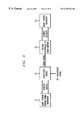
- FIG. 3shows in block diagram form a preferred type of control circuitry for the embodiment of FIG. 2 .
- signal generator 51signals from each combination of HEMS steerable mirror 35 and a sensing electrode 41 (there being four such electrodes for one mirror 35 ) are combined in known fashion or sent in a pair of signal paths to capacitance bridge 52 , which separately receives a signal representing a reference capacitance. This signal also represents a desired deflection of mirror 35 , as determined by external control circuitry.
- An error signal from the balance terminals of capacitance bridge 52is sent to voltage controller 53 , which generates and applies a corrective signal to deflection electrode 37 for MEMS mirror 35 .
- Electrode 37 and MEMS mirror 35form a MEMS control capacitor 54 .
- Each of signal generator 51 , capacitance bridge 52 , and voltage controller 53can be implemented in any of several known manners, to the extent that they are mutually compatible.
- the signal to set the reference capacitance of bridge 52is calibrated for a particular steerable mirror 35 by observing the spots to which that mirror 35 reflects an optical beam.
- the signal to set the reference capacitance of bridge 52is calibrated for a particular steerable mirror 35 by observing the spots to which that mirror 35 reflects an optical beam.
- an array (not shown) of steerable mirrorsseparate calibrations for each mirror is stored in a memory (not shown) of the external control circuitry.
- Feedback circuitry for the embodiment of FIG. 1can also be implemented in any of several known manners, including using a bridge analogous to that of FIG. 3 .
- MEMS device 61has a semiconductor wafer substrate forming a base 63 for a MEMS element array, including MEMS steerable mirrors 65 , 66 , 67 , and 68 , as typical elements. These mirrors are suspended on springs 69 , 70 , 71 , and 72 , respectively, which support the mirrors in nominal positions parallel to base 63 .
- Plate electrodes 81 , 82 , 83 , and 84respectively form a pair of parallel plate capacitors with the conductive back of MEMS steerable mirror 65 , 66 , 67 , and 68 .
- Electrodes 81 , 82 , 83 , and 84are arranged so that opposite polarity voltages apply a deflection torque to the respective MEMS steerable mirror.
- Position detection capacitorsare formed with the back of MEMS steerable mirrors 65 , 66 , 67 , and 68 , by auxiliary electrodes 91 , 92 , 93 , and 94 , which may be separate from electrodes 81 , 82 , 83 , and 84 , or may be extensions thereof
- auxiliary electrodes 91 , 92 , 93 , and 94which may be separate from electrodes 81 , 82 , 83 , and 84 , or may be extensions thereof
- a relatively high frequencyis applied (by a test signal generator not shown) across each respective capacitor.
- Another relatively low frequencyis applied between the back of each MEMS steerable mirror and the respective one of drive electrodes 81 , 82 , 83 , and 84 . That frequency is low enough to produce a deflection of the MEMS steerable mirror.
- each element of the array of FIG. 4is like that of the corresponding element of FIG. 2 . It should be apparent that the four-element array of FIG. 4 can be extended to a large number of elements. In such an array, each movable MEMS element has in direct association a plurality of sensors that serve only it.
Landscapes
- Physics & Mathematics (AREA)
- General Physics & Mathematics (AREA)
- Optics & Photonics (AREA)
- Micromachines (AREA)
Abstract
Description
Claims (16)
Priority Applications (1)
| Application Number | Priority Date | Filing Date | Title |
|---|---|---|---|
| US09/400,719US6275326B1 (en) | 1999-09-21 | 1999-09-21 | Control arrangement for microelectromechanical devices and systems |
Applications Claiming Priority (1)
| Application Number | Priority Date | Filing Date | Title |
|---|---|---|---|
| US09/400,719US6275326B1 (en) | 1999-09-21 | 1999-09-21 | Control arrangement for microelectromechanical devices and systems |
Publications (1)
| Publication Number | Publication Date |
|---|---|
| US6275326B1true US6275326B1 (en) | 2001-08-14 |
Family
ID=23584723
Family Applications (1)
| Application Number | Title | Priority Date | Filing Date |
|---|---|---|---|
| US09/400,719Expired - LifetimeUS6275326B1 (en) | 1999-09-21 | 1999-09-21 | Control arrangement for microelectromechanical devices and systems |
Country Status (1)
| Country | Link |
|---|---|
| US (1) | US6275326B1 (en) |
Cited By (87)
| Publication number | Priority date | Publication date | Assignee | Title |
|---|---|---|---|---|
| WO2002059679A1 (en)* | 2001-01-25 | 2002-08-01 | Nayna Networks, Inc. | Integrated mirror array and circuit device |
| US20020101646A1 (en)* | 2001-01-31 | 2002-08-01 | Takayuki Ide | Deformable mirror having displacement detecting function |
| US6522445B1 (en)* | 1999-11-04 | 2003-02-18 | Lucent Technologies Inc. | Feedback sensor for M.E.M.S. mirrors |
| US6538802B2 (en)* | 2001-07-31 | 2003-03-25 | Axsun Technologies, Inc | System and method for tilt mirror calibration due to capacitive sensor drift |
| US20030075992A1 (en)* | 2001-10-19 | 2003-04-24 | Kouns Heath Elliot | Utilizing feedback for control of switch actuators |
| US6560002B2 (en)* | 2000-11-15 | 2003-05-06 | Japan Aviation Electronics Industry, Limited | Optical switch |
| US20030123046A1 (en)* | 2001-12-12 | 2003-07-03 | Heaton Mark W. | High performance controller for shifting resonance in micro-electro-mechanical systems (MEMS) devices |
| US20030174376A1 (en)* | 2002-03-12 | 2003-09-18 | Corning Incorporated | Pointing angle control of electrostatic micro mirrors with modified sliding mode control algorithm for precision control |
| US20030184844A1 (en)* | 2002-03-12 | 2003-10-02 | Corning Intellisense | Pointing angle control of electrostatic micro mirrors |
| US20030210453A1 (en)* | 2002-05-09 | 2003-11-13 | Nec Corporation | Optical device and a movable mirror driving method |
| US20030225463A1 (en)* | 2002-06-03 | 2003-12-04 | Oettinger Eric G. | System identification to improve control of a micro-electro-mechanical mirror |
| US6690847B2 (en)* | 2000-09-19 | 2004-02-10 | Newport Opticom, Inc. | Optical switching element having movable optically transmissive microstructure |
| US6710350B2 (en) | 2002-03-05 | 2004-03-23 | Ge Medical Systems Information Technologies, Inc. | Radiation detector with microphotonic optical switches to route light in an imaging system |
| US6711317B2 (en)* | 2001-01-25 | 2004-03-23 | Lucent Technologies Inc. | Resiliently packaged MEMs device and method for making same |
| US20040061925A1 (en)* | 2002-09-30 | 2004-04-01 | Azarov Alexei V. | Orientation stabilization for MEMS devices |
| US20040063325A1 (en)* | 2002-01-11 | 2004-04-01 | Masami Urano | Semiconductor device having MEMS |
| US20040061619A1 (en)* | 2002-09-30 | 2004-04-01 | Jungsang Kim | Piezo-resistive sensing of mirror position in an optical switch |
| US20040061618A1 (en)* | 2002-09-30 | 2004-04-01 | Martin Haueis | Sensing of mirror position in an optical switch |
| US20040071395A1 (en)* | 2001-04-17 | 2004-04-15 | Newport Opticom, Inc. | Low loss optical switching system |
| US6771851B1 (en) | 2001-06-19 | 2004-08-03 | Nayna Networks | Fast switching method for a micro-mirror device for optical switching applications |
| US6798213B2 (en) | 2002-07-30 | 2004-09-28 | Oes, Inc. | Circuit analyzer with component testing capability |
| US20040258361A1 (en)* | 2003-05-01 | 2004-12-23 | Newport Opticom, Inc. | Low-loss optical waveguide crossovers using an out-of-plane waveguide |
| US20050046659A1 (en)* | 1999-06-30 | 2005-03-03 | Kia Silverbrook | Method of detecting a fault condition in a micro-electromechanical device |
| US20050063639A1 (en)* | 2002-02-08 | 2005-03-24 | Newport Opticom, Inc. | Structures that correct for thermal distortion in an optical device formed of thermally dissimilar materials |
| US20050206991A1 (en)* | 2003-12-09 | 2005-09-22 | Clarence Chui | System and method for addressing a MEMS display |
| US6950223B2 (en)* | 2003-01-15 | 2005-09-27 | Reflectivity, Inc | Multiple hinge MEMS device |
| US6990264B2 (en) | 2000-09-19 | 2006-01-24 | Telkamp Arthur R | 1×N or N×1 optical switch having a plurality of movable light guiding microstructures |
| US20060039051A1 (en)* | 2004-07-28 | 2006-02-23 | Sony Corporation | Hologram apparatus, positioning method for spatial light modulator and image pickup device, and hologram recording material |
| US20060067653A1 (en)* | 2004-09-27 | 2006-03-30 | Gally Brian J | Method and system for driving interferometric modulators |
| US20060072187A1 (en)* | 2004-10-05 | 2006-04-06 | Mckinnell James | Systems and methods for amorphous flexures in micro-electro mechanical systems |
| US20060077127A1 (en)* | 2004-09-27 | 2006-04-13 | Sampsell Jeffrey B | Controller and driver features for bi-stable display |
| US7031082B2 (en)* | 2003-02-17 | 2006-04-18 | Canon Kabushiki Kaisha | Retainer, exposure apparatus, and device fabrication method |
| US7136213B2 (en) | 2004-09-27 | 2006-11-14 | Idc, Llc | Interferometric modulators having charge persistence |
| US20070029174A1 (en)* | 2004-02-19 | 2007-02-08 | Eaton Automotive B.V. | Mechatronic control system |
| US20070041078A1 (en)* | 2005-08-16 | 2007-02-22 | Pan Shaoher X | Addressing circuit and method for bi-directional micro-mirror array |
| US7190509B2 (en) | 2001-11-07 | 2007-03-13 | Trex Enterprises Corp. | Optically addressed MEMS |
| US7196837B2 (en) | 2003-12-09 | 2007-03-27 | Idc, Llc | Area array modulation and lead reduction in interferometric modulators |
| US7310179B2 (en) | 2004-09-27 | 2007-12-18 | Idc, Llc | Method and device for selective adjustment of hysteresis window |
| US7345805B2 (en) | 2004-09-27 | 2008-03-18 | Idc, Llc | Interferometric modulator array with integrated MEMS electrical switches |
| US7355779B2 (en) | 2005-09-02 | 2008-04-08 | Idc, Llc | Method and system for driving MEMS display elements |
| US7388706B2 (en) | 1995-05-01 | 2008-06-17 | Idc, Llc | Photonic MEMS and structures |
| US7446927B2 (en) | 2004-09-27 | 2008-11-04 | Idc, Llc | MEMS switch with set and latch electrodes |
| US7471444B2 (en) | 1996-12-19 | 2008-12-30 | Idc, Llc | Interferometric modulation of radiation |
| US7486429B2 (en) | 2004-09-27 | 2009-02-03 | Idc, Llc | Method and device for multistate interferometric light modulation |
| US7499208B2 (en) | 2004-08-27 | 2009-03-03 | Udc, Llc | Current mode display driver circuit realization feature |
| US7515147B2 (en) | 2004-08-27 | 2009-04-07 | Idc, Llc | Staggered column drive circuit systems and methods |
| US7532195B2 (en) | 2004-09-27 | 2009-05-12 | Idc, Llc | Method and system for reducing power consumption in a display |
| US7545550B2 (en) | 2004-09-27 | 2009-06-09 | Idc, Llc | Systems and methods of actuating MEMS display elements |
| US7551159B2 (en) | 2004-08-27 | 2009-06-23 | Idc, Llc | System and method of sensing actuation and release voltages of an interferometric modulator |
| US7560299B2 (en) | 2004-08-27 | 2009-07-14 | Idc, Llc | Systems and methods of actuating MEMS display elements |
| US20090204350A1 (en)* | 2008-02-11 | 2009-08-13 | Qualcomms Technologies, Inc, | Methods for measurement and characterization of interferometric modulators |
| US20090201034A1 (en)* | 2008-02-11 | 2009-08-13 | Qualcomm Mems Technologies, Inc. | Methods for measurement and characterization of interferometric modulators |
| US20090201242A1 (en)* | 2008-02-11 | 2009-08-13 | Qualcomm Mems Technologies, Inc. | Sensing to determine pixel state in a passively addressed display array |
| US20090201282A1 (en)* | 2008-02-11 | 2009-08-13 | Qualcomm Mems Technologies, Inc | Methods of tuning interferometric modulator displays |
| US20090204349A1 (en)* | 2008-02-11 | 2009-08-13 | Qualcomm Mems Technologies, Inc. | Measurement and apparatus for electrical measurement of electrical drive parameters for a mems based display |
| US20090213107A1 (en)* | 2008-02-11 | 2009-08-27 | Qualcomm Mems Technologies, Inc, | Method and apparatus for sensing, measurement or characterization of display elements integrated with the display drive scheme, and system and applications using the same |
| US7626581B2 (en) | 2004-09-27 | 2009-12-01 | Idc, Llc | Device and method for display memory using manipulation of mechanical response |
| US7702192B2 (en) | 2006-06-21 | 2010-04-20 | Qualcomm Mems Technologies, Inc. | Systems and methods for driving MEMS display |
| US7724993B2 (en) | 2004-09-27 | 2010-05-25 | Qualcomm Mems Technologies, Inc. | MEMS switches with deforming membranes |
| US7777715B2 (en) | 2006-06-29 | 2010-08-17 | Qualcomm Mems Technologies, Inc. | Passive circuits for de-multiplexing display inputs |
| US7843410B2 (en) | 2004-09-27 | 2010-11-30 | Qualcomm Mems Technologies, Inc. | Method and device for electrically programmable display |
| US7889163B2 (en) | 2004-08-27 | 2011-02-15 | Qualcomm Mems Technologies, Inc. | Drive method for MEMS devices |
| US7920136B2 (en) | 2005-05-05 | 2011-04-05 | Qualcomm Mems Technologies, Inc. | System and method of driving a MEMS display device |
| US7948457B2 (en) | 2005-05-05 | 2011-05-24 | Qualcomm Mems Technologies, Inc. | Systems and methods of actuating MEMS display elements |
| US20110181931A1 (en)* | 2008-07-02 | 2011-07-28 | Btendo Ltd. | mems device comprising oscillations measurements means |
| US8027800B2 (en) | 2008-06-24 | 2011-09-27 | Qualcomm Mems Technologies, Inc. | Apparatus and method for testing a panel of interferometric modulators |
| US8049713B2 (en) | 2006-04-24 | 2011-11-01 | Qualcomm Mems Technologies, Inc. | Power consumption optimized display update |
| US8174469B2 (en) | 2005-05-05 | 2012-05-08 | Qualcomm Mems Technologies, Inc. | Dynamic driver IC and display panel configuration |
| US8194056B2 (en) | 2006-02-09 | 2012-06-05 | Qualcomm Mems Technologies Inc. | Method and system for writing data to MEMS display elements |
| US8310441B2 (en) | 2004-09-27 | 2012-11-13 | Qualcomm Mems Technologies, Inc. | Method and system for writing data to MEMS display elements |
| US8391630B2 (en) | 2005-12-22 | 2013-03-05 | Qualcomm Mems Technologies, Inc. | System and method for power reduction when decompressing video streams for interferometric modulator displays |
| US8736590B2 (en) | 2009-03-27 | 2014-05-27 | Qualcomm Mems Technologies, Inc. | Low voltage driver scheme for interferometric modulators |
| US20140145551A1 (en)* | 2012-11-29 | 2014-05-29 | Seiko Epson Corporation | Vibrator, manufacturing method of vibrator, electronic apparatus, and moving object |
| US8878825B2 (en) | 2004-09-27 | 2014-11-04 | Qualcomm Mems Technologies, Inc. | System and method for providing a variable refresh rate of an interferometric modulator display |
| US8928967B2 (en) | 1998-04-08 | 2015-01-06 | Qualcomm Mems Technologies, Inc. | Method and device for modulating light |
| US8971675B2 (en) | 2006-01-13 | 2015-03-03 | Qualcomm Mems Technologies, Inc. | Interconnect structure for MEMS device |
| US9110289B2 (en) | 1998-04-08 | 2015-08-18 | Qualcomm Mems Technologies, Inc. | Device for modulating light with multiple electrodes |
| US20170031154A1 (en)* | 2015-07-28 | 2017-02-02 | Kabushiki Kaisha Toshiba | Optical scanner, optical scanning method and non-transient recording medium |
| US20170139202A1 (en)* | 2014-06-20 | 2017-05-18 | Newson Nv | Apparatus and Method for Positioning an Optical Element |
| DE102015003188B4 (en) | 2014-03-31 | 2018-06-14 | Kabushiki Kaisha Toyota Chuo Kenkyusho | MEMS device |
| WO2021257147A1 (en)* | 2020-06-19 | 2021-12-23 | Beijing Voyager Technology Co., Ltd. | Systems and methods for detecting resonant frequency of mems mirrors |
| US20220099982A1 (en)* | 2018-12-07 | 2022-03-31 | Avegant Corp. | Steerable Positioning Element |
| KR20230036935A (en) | 2021-09-08 | 2023-03-15 | 주식회사 위멤스 | Optical Scanner Including Rotation Angle Sensor of Mirror and Detecting Method thereof |
| US12032174B2 (en) | 2019-03-29 | 2024-07-09 | Avegant Corp. | Steerable hybrid display using a waveguide |
| US12092828B2 (en) | 2020-01-06 | 2024-09-17 | Avegant Corp. | Head mounted system with color specific modulation |
| US12292565B2 (en) | 2019-04-18 | 2025-05-06 | Eyeway Vision Ltd. | MEMS based light deflecting device and method |
| US12360378B2 (en) | 2017-03-27 | 2025-07-15 | Avegant Corp. | Steerable high-resolution display |
Citations (6)
| Publication number | Priority date | Publication date | Assignee | Title |
|---|---|---|---|---|
| US4560925A (en)* | 1982-09-30 | 1985-12-24 | Burroughs Corporation | Mirror position sensor and associated pivot suspension for improved track selection in optical data disk system |
| US4738500A (en)* | 1985-11-02 | 1988-04-19 | Carl-Zeiss-Stiftung | Electromagnetically driven oscillating mirror |
| US5283682A (en)* | 1992-10-06 | 1994-02-01 | Ball Corporation | Reactionless scanning and positioning system |
| US5392151A (en)* | 1991-12-23 | 1995-02-21 | Texas Instruments Incorporated | Method and apparatus for steering light |
| US5408253A (en)* | 1992-08-03 | 1995-04-18 | Eastman Kodak Company | Integrated galvanometer scanning device |
| US6108118A (en)* | 1998-07-09 | 2000-08-22 | Olympus Optical Co., Ltd. | Optical deflector |
- 1999
- 1999-09-21USUS09/400,719patent/US6275326B1/ennot_activeExpired - Lifetime
Patent Citations (6)
| Publication number | Priority date | Publication date | Assignee | Title |
|---|---|---|---|---|
| US4560925A (en)* | 1982-09-30 | 1985-12-24 | Burroughs Corporation | Mirror position sensor and associated pivot suspension for improved track selection in optical data disk system |
| US4738500A (en)* | 1985-11-02 | 1988-04-19 | Carl-Zeiss-Stiftung | Electromagnetically driven oscillating mirror |
| US5392151A (en)* | 1991-12-23 | 1995-02-21 | Texas Instruments Incorporated | Method and apparatus for steering light |
| US5408253A (en)* | 1992-08-03 | 1995-04-18 | Eastman Kodak Company | Integrated galvanometer scanning device |
| US5283682A (en)* | 1992-10-06 | 1994-02-01 | Ball Corporation | Reactionless scanning and positioning system |
| US6108118A (en)* | 1998-07-09 | 2000-08-22 | Olympus Optical Co., Ltd. | Optical deflector |
Cited By (153)
| Publication number | Priority date | Publication date | Assignee | Title |
|---|---|---|---|---|
| US7388706B2 (en) | 1995-05-01 | 2008-06-17 | Idc, Llc | Photonic MEMS and structures |
| US7471444B2 (en) | 1996-12-19 | 2008-12-30 | Idc, Llc | Interferometric modulation of radiation |
| US9110289B2 (en) | 1998-04-08 | 2015-08-18 | Qualcomm Mems Technologies, Inc. | Device for modulating light with multiple electrodes |
| US8928967B2 (en) | 1998-04-08 | 2015-01-06 | Qualcomm Mems Technologies, Inc. | Method and device for modulating light |
| US20050046659A1 (en)* | 1999-06-30 | 2005-03-03 | Kia Silverbrook | Method of detecting a fault condition in a micro-electromechanical device |
| US7635177B2 (en) | 1999-06-30 | 2009-12-22 | Silverbrook Research Pty Ltd | Inkjet nozzle device with cantilevered actuating arm |
| US20050275492A1 (en)* | 1999-06-30 | 2005-12-15 | Silverbrook Research Pty Ltd | Mems fluid ejection device configured for detecting a fault condition |
| US6969142B2 (en)* | 1999-06-30 | 2005-11-29 | Silverbrook Research, Pty Ltd | Method of detecting a fault condition in a micro-electromechanical device |
| US20080211875A1 (en)* | 1999-06-30 | 2008-09-04 | Silverbrook Research Pty Ltd | Inkjet nozzle device with cantilevered actuating arm |
| US8317301B2 (en) | 1999-06-30 | 2012-11-27 | Zamtec Limited | Printing nozzle arrangement having fault detector |
| US20060130904A1 (en)* | 1999-06-30 | 2006-06-22 | Silverbrook Research Pty Ltd | Fluid ejection device with inner and outer arms |
| US7128093B2 (en) | 1999-06-30 | 2006-10-31 | Silverbrook Research Pty Ltd | MEMS fluid ejection device configured for detecting a fault condition |
| US8038252B2 (en) | 1999-06-30 | 2011-10-18 | Silverbrook Research Pty Ltd | Method of detecting MEM device faults with single current pulse |
| US20100073429A1 (en)* | 1999-06-30 | 2010-03-25 | Silverbrook Research Pty Ltd | Inkjet Nozzle Device With Cantilevered Actuating Arm |
| US7210666B2 (en) | 1999-06-30 | 2007-05-01 | Silverbrook Research Pty Ltd | Fluid ejection device with inner and outer arms |
| US6522445B1 (en)* | 1999-11-04 | 2003-02-18 | Lucent Technologies Inc. | Feedback sensor for M.E.M.S. mirrors |
| US6525864B1 (en)* | 2000-07-20 | 2003-02-25 | Nayna Networks, Inc. | Integrated mirror array and circuit device |
| US20040141683A1 (en)* | 2000-09-19 | 2004-07-22 | Newport Opticom, Inc. | Optical switching element having movable optically transmissive microstructure |
| US6690847B2 (en)* | 2000-09-19 | 2004-02-10 | Newport Opticom, Inc. | Optical switching element having movable optically transmissive microstructure |
| US6990264B2 (en) | 2000-09-19 | 2006-01-24 | Telkamp Arthur R | 1×N or N×1 optical switch having a plurality of movable light guiding microstructures |
| US6560002B2 (en)* | 2000-11-15 | 2003-05-06 | Japan Aviation Electronics Industry, Limited | Optical switch |
| US6711317B2 (en)* | 2001-01-25 | 2004-03-23 | Lucent Technologies Inc. | Resiliently packaged MEMs device and method for making same |
| WO2002059679A1 (en)* | 2001-01-25 | 2002-08-01 | Nayna Networks, Inc. | Integrated mirror array and circuit device |
| US20020101646A1 (en)* | 2001-01-31 | 2002-08-01 | Takayuki Ide | Deformable mirror having displacement detecting function |
| US7190500B2 (en)* | 2001-01-31 | 2007-03-13 | Olympus Corporation | Deformable mirror having displacement detecting function |
| US7003188B2 (en) | 2001-04-17 | 2006-02-21 | Ying Wen Hsu | Low loss optical switching system |
| US20040071395A1 (en)* | 2001-04-17 | 2004-04-15 | Newport Opticom, Inc. | Low loss optical switching system |
| US6771851B1 (en) | 2001-06-19 | 2004-08-03 | Nayna Networks | Fast switching method for a micro-mirror device for optical switching applications |
| US6538802B2 (en)* | 2001-07-31 | 2003-03-25 | Axsun Technologies, Inc | System and method for tilt mirror calibration due to capacitive sensor drift |
| US20030075992A1 (en)* | 2001-10-19 | 2003-04-24 | Kouns Heath Elliot | Utilizing feedback for control of switch actuators |
| US20080031569A1 (en)* | 2001-11-07 | 2008-02-07 | Trex Enterprises Corp. | Optically addressed MEMS |
| US7460294B2 (en) | 2001-11-07 | 2008-12-02 | Trex Enterprises Corp | Optically addressed MEMS |
| US7190509B2 (en) | 2001-11-07 | 2007-03-13 | Trex Enterprises Corp. | Optically addressed MEMS |
| US7047097B2 (en)* | 2001-12-12 | 2006-05-16 | Texas Instruments Incorporated | High performance controller for shifting resonance in micro-electro-mechanical systems (MEMS) devices |
| US20030123046A1 (en)* | 2001-12-12 | 2003-07-03 | Heaton Mark W. | High performance controller for shifting resonance in micro-electro-mechanical systems (MEMS) devices |
| US20040063325A1 (en)* | 2002-01-11 | 2004-04-01 | Masami Urano | Semiconductor device having MEMS |
| US20050063639A1 (en)* | 2002-02-08 | 2005-03-24 | Newport Opticom, Inc. | Structures that correct for thermal distortion in an optical device formed of thermally dissimilar materials |
| US20050100283A1 (en)* | 2002-02-08 | 2005-05-12 | Newport Opticom, Inc. | Structures that correct for thermal distortion in an optical device formed of thermally dissimilar materials |
| US6710350B2 (en) | 2002-03-05 | 2004-03-23 | Ge Medical Systems Information Technologies, Inc. | Radiation detector with microphotonic optical switches to route light in an imaging system |
| US6958850B2 (en) | 2002-03-12 | 2005-10-25 | Corning Incorporated | Pointing angle control of electrostatic micro mirrors with modified sliding mode control algorithm for precision control |
| US20030174376A1 (en)* | 2002-03-12 | 2003-09-18 | Corning Incorporated | Pointing angle control of electrostatic micro mirrors with modified sliding mode control algorithm for precision control |
| US20030184844A1 (en)* | 2002-03-12 | 2003-10-02 | Corning Intellisense | Pointing angle control of electrostatic micro mirrors |
| US6985271B2 (en)* | 2002-03-12 | 2006-01-10 | Corning Incorporated | Pointing angle control of electrostatic micro mirrors |
| US20030210453A1 (en)* | 2002-05-09 | 2003-11-13 | Nec Corporation | Optical device and a movable mirror driving method |
| EP1369732A3 (en)* | 2002-06-03 | 2005-02-16 | Texas Instruments Incorporated | System identification to improve control of a micro-electro-mechanical mirror |
| US20030225463A1 (en)* | 2002-06-03 | 2003-12-04 | Oettinger Eric G. | System identification to improve control of a micro-electro-mechanical mirror |
| US6708082B2 (en)* | 2002-06-03 | 2004-03-16 | Texas Instruments Incorporated | System identification to improve control of a micro-electro-mechanical mirror |
| US6798213B2 (en) | 2002-07-30 | 2004-09-28 | Oes, Inc. | Circuit analyzer with component testing capability |
| US20060115920A1 (en)* | 2002-09-19 | 2006-06-01 | Masami Urano | Semiconductor device having MEMS |
| US7208809B2 (en) | 2002-09-19 | 2007-04-24 | Nippon Telegraph And Telephone Corporation | Semiconductor device having MEMS |
| US7482196B2 (en)* | 2002-09-19 | 2009-01-27 | Nippon Telegraph And Telephone Corporation | Method of manufacturing a semiconductor device having MEMS |
| US6911913B2 (en)* | 2002-09-30 | 2005-06-28 | Lucent Technologies Inc. | Piezo-resistive sensing of mirror position in an optical switch |
| US20040061925A1 (en)* | 2002-09-30 | 2004-04-01 | Azarov Alexei V. | Orientation stabilization for MEMS devices |
| US20040061619A1 (en)* | 2002-09-30 | 2004-04-01 | Jungsang Kim | Piezo-resistive sensing of mirror position in an optical switch |
| US6888470B2 (en) | 2002-09-30 | 2005-05-03 | Lucent Technologies Inc. | Sensing of mirror position in an optical switch |
| US6768571B2 (en)* | 2002-09-30 | 2004-07-27 | Lucent Technologies Inc. | Orientation stabilization for MEMS devices |
| US20040061618A1 (en)* | 2002-09-30 | 2004-04-01 | Martin Haueis | Sensing of mirror position in an optical switch |
| US6950223B2 (en)* | 2003-01-15 | 2005-09-27 | Reflectivity, Inc | Multiple hinge MEMS device |
| US7031082B2 (en)* | 2003-02-17 | 2006-04-18 | Canon Kabushiki Kaisha | Retainer, exposure apparatus, and device fabrication method |
| US20040258361A1 (en)* | 2003-05-01 | 2004-12-23 | Newport Opticom, Inc. | Low-loss optical waveguide crossovers using an out-of-plane waveguide |
| US7215854B2 (en) | 2003-05-01 | 2007-05-08 | Gemfire Corporation | Low-loss optical waveguide crossovers using an out-of-plane waveguide |
| US7062130B2 (en) | 2003-05-01 | 2006-06-13 | Arthur Telkamp | Low-loss optical waveguide crossovers using an out-of-plane waveguide |
| US20050271320A1 (en)* | 2003-05-01 | 2005-12-08 | Gemfire Corporation | Low-loss optical waveguide crossovers using an out-of-plane waveguide |
| US7142346B2 (en) | 2003-12-09 | 2006-11-28 | Idc, Llc | System and method for addressing a MEMS display |
| US7242512B2 (en) | 2003-12-09 | 2007-07-10 | Idc, Llc | System and method for addressing a MEMS display |
| US20050206991A1 (en)* | 2003-12-09 | 2005-09-22 | Clarence Chui | System and method for addressing a MEMS display |
| US7196837B2 (en) | 2003-12-09 | 2007-03-27 | Idc, Llc | Area array modulation and lead reduction in interferometric modulators |
| US7388697B2 (en) | 2003-12-09 | 2008-06-17 | Idc, Llc | System and method for addressing a MEMS display |
| US20070029174A1 (en)* | 2004-02-19 | 2007-02-08 | Eaton Automotive B.V. | Mechatronic control system |
| US20060039051A1 (en)* | 2004-07-28 | 2006-02-23 | Sony Corporation | Hologram apparatus, positioning method for spatial light modulator and image pickup device, and hologram recording material |
| US7515147B2 (en) | 2004-08-27 | 2009-04-07 | Idc, Llc | Staggered column drive circuit systems and methods |
| US20090224748A1 (en)* | 2004-08-27 | 2009-09-10 | Idc, Llc | System and method of sensing actuation and release voltages of an interferometric modulator |
| US8207920B2 (en) | 2004-08-27 | 2012-06-26 | Qualcomm Mems Technologies, Inc. | System and method of sensing actuation and release voltages of an interferometric modulator |
| US7928940B2 (en) | 2004-08-27 | 2011-04-19 | Qualcomm Mems Technologies, Inc. | Drive method for MEMS devices |
| US7889163B2 (en) | 2004-08-27 | 2011-02-15 | Qualcomm Mems Technologies, Inc. | Drive method for MEMS devices |
| US8487846B2 (en) | 2004-08-27 | 2013-07-16 | Qualcomm Mems Technologies, Inc. | System and method of sensing actuation and release voltages of an interferometric modulator |
| US7499208B2 (en) | 2004-08-27 | 2009-03-03 | Udc, Llc | Current mode display driver circuit realization feature |
| US20130300439A1 (en)* | 2004-08-27 | 2013-11-14 | Qualcomm Mems Technologies, Inc. | System and method of sensing actuation and release voltages of an interferometric modulator |
| US7560299B2 (en) | 2004-08-27 | 2009-07-14 | Idc, Llc | Systems and methods of actuating MEMS display elements |
| US7551159B2 (en) | 2004-08-27 | 2009-06-23 | Idc, Llc | System and method of sensing actuation and release voltages of an interferometric modulator |
| US7667884B2 (en) | 2004-09-27 | 2010-02-23 | Qualcomm Mems Technologies, Inc. | Interferometric modulators having charge persistence |
| US7675669B2 (en) | 2004-09-27 | 2010-03-09 | Qualcomm Mems Technologies, Inc. | Method and system for driving interferometric modulators |
| US20060067653A1 (en)* | 2004-09-27 | 2006-03-30 | Gally Brian J | Method and system for driving interferometric modulators |
| US7136213B2 (en) | 2004-09-27 | 2006-11-14 | Idc, Llc | Interferometric modulators having charge persistence |
| US8310441B2 (en) | 2004-09-27 | 2012-11-13 | Qualcomm Mems Technologies, Inc. | Method and system for writing data to MEMS display elements |
| US8878771B2 (en) | 2004-09-27 | 2014-11-04 | Qualcomm Mems Technologies, Inc. | Method and system for reducing power consumption in a display |
| US8878825B2 (en) | 2004-09-27 | 2014-11-04 | Qualcomm Mems Technologies, Inc. | System and method for providing a variable refresh rate of an interferometric modulator display |
| US8791897B2 (en) | 2004-09-27 | 2014-07-29 | Qualcomm Mems Technologies, Inc. | Method and system for writing data to MEMS display elements |
| US7310179B2 (en) | 2004-09-27 | 2007-12-18 | Idc, Llc | Method and device for selective adjustment of hysteresis window |
| US7486429B2 (en) | 2004-09-27 | 2009-02-03 | Idc, Llc | Method and device for multistate interferometric light modulation |
| US7446927B2 (en) | 2004-09-27 | 2008-11-04 | Idc, Llc | MEMS switch with set and latch electrodes |
| US7345805B2 (en) | 2004-09-27 | 2008-03-18 | Idc, Llc | Interferometric modulator array with integrated MEMS electrical switches |
| US7843410B2 (en) | 2004-09-27 | 2010-11-30 | Qualcomm Mems Technologies, Inc. | Method and device for electrically programmable display |
| US7626581B2 (en) | 2004-09-27 | 2009-12-01 | Idc, Llc | Device and method for display memory using manipulation of mechanical response |
| US7724993B2 (en) | 2004-09-27 | 2010-05-25 | Qualcomm Mems Technologies, Inc. | MEMS switches with deforming membranes |
| US20060077127A1 (en)* | 2004-09-27 | 2006-04-13 | Sampsell Jeffrey B | Controller and driver features for bi-stable display |
| US7532195B2 (en) | 2004-09-27 | 2009-05-12 | Idc, Llc | Method and system for reducing power consumption in a display |
| US7679627B2 (en) | 2004-09-27 | 2010-03-16 | Qualcomm Mems Technologies, Inc. | Controller and driver features for bi-stable display |
| US7545550B2 (en) | 2004-09-27 | 2009-06-09 | Idc, Llc | Systems and methods of actuating MEMS display elements |
| US7184193B2 (en)* | 2004-10-05 | 2007-02-27 | Hewlett-Packard Development Company, L.P. | Systems and methods for amorphous flexures in micro-electro mechanical systems |
| US20060072187A1 (en)* | 2004-10-05 | 2006-04-06 | Mckinnell James | Systems and methods for amorphous flexures in micro-electro mechanical systems |
| US7920136B2 (en) | 2005-05-05 | 2011-04-05 | Qualcomm Mems Technologies, Inc. | System and method of driving a MEMS display device |
| US8174469B2 (en) | 2005-05-05 | 2012-05-08 | Qualcomm Mems Technologies, Inc. | Dynamic driver IC and display panel configuration |
| US7948457B2 (en) | 2005-05-05 | 2011-05-24 | Qualcomm Mems Technologies, Inc. | Systems and methods of actuating MEMS display elements |
| US20070041078A1 (en)* | 2005-08-16 | 2007-02-22 | Pan Shaoher X | Addressing circuit and method for bi-directional micro-mirror array |
| US7423798B2 (en)* | 2005-08-16 | 2008-09-09 | Spatial Photonics, Inc. | Addressing circuit and method for bi-directional micro-mirror array |
| US7355779B2 (en) | 2005-09-02 | 2008-04-08 | Idc, Llc | Method and system for driving MEMS display elements |
| US8391630B2 (en) | 2005-12-22 | 2013-03-05 | Qualcomm Mems Technologies, Inc. | System and method for power reduction when decompressing video streams for interferometric modulator displays |
| US8971675B2 (en) | 2006-01-13 | 2015-03-03 | Qualcomm Mems Technologies, Inc. | Interconnect structure for MEMS device |
| US8194056B2 (en) | 2006-02-09 | 2012-06-05 | Qualcomm Mems Technologies Inc. | Method and system for writing data to MEMS display elements |
| US8049713B2 (en) | 2006-04-24 | 2011-11-01 | Qualcomm Mems Technologies, Inc. | Power consumption optimized display update |
| US7702192B2 (en) | 2006-06-21 | 2010-04-20 | Qualcomm Mems Technologies, Inc. | Systems and methods for driving MEMS display |
| US7777715B2 (en) | 2006-06-29 | 2010-08-17 | Qualcomm Mems Technologies, Inc. | Passive circuits for de-multiplexing display inputs |
| US20090213107A1 (en)* | 2008-02-11 | 2009-08-27 | Qualcomm Mems Technologies, Inc, | Method and apparatus for sensing, measurement or characterization of display elements integrated with the display drive scheme, and system and applications using the same |
| US8775107B2 (en) | 2008-02-11 | 2014-07-08 | Qualcomm Mems Technologies, Inc. | Measurement and apparatus for electrical measurement of electrical drive parameters for a MEMS based display |
| US8115471B2 (en) | 2008-02-11 | 2012-02-14 | Qualcomm Mems Technologies, Inc. | Methods for measurement and characterization of interferometric modulators |
| US8204703B2 (en) | 2008-02-11 | 2012-06-19 | Qualcomm Mems Technologies, Inc. | Measurement and apparatus for electrical measurement of electrical drive parameters for a MEMS based display |
| US20090204350A1 (en)* | 2008-02-11 | 2009-08-13 | Qualcomms Technologies, Inc, | Methods for measurement and characterization of interferometric modulators |
| US8258800B2 (en) | 2008-02-11 | 2012-09-04 | Qualcomm Mems Technologies, Inc. | Methods for measurement and characterization of interferometric modulators |
| US8274299B2 (en) | 2008-02-11 | 2012-09-25 | Qualcomm Mems Technologies, Inc. | Methods for measurement and characterization of interferometric modulators |
| US20090201034A1 (en)* | 2008-02-11 | 2009-08-13 | Qualcomm Mems Technologies, Inc. | Methods for measurement and characterization of interferometric modulators |
| US20100039409A1 (en)* | 2008-02-11 | 2010-02-18 | Qualcomm Mems Technologies, Inc. | Method and apparatus for sensing, measurement or characterization of display elements integrated with the display drive scheme, and system and applications using the same |
| US8355883B2 (en) | 2008-02-11 | 2013-01-15 | Qualcomm Mems Technologies, Inc. | Measurement and apparatus for electrical measurement of electrical drive parameters for a MEMS based display |
| US8386201B2 (en)* | 2008-02-11 | 2013-02-26 | Qualcomm Mems Technologies, Inc. | Methods for measurement and characterization of interferometric modulators |
| US20090251157A1 (en)* | 2008-02-11 | 2009-10-08 | Qualcomm Mems Technologies, Inc. | Methods for measurement and characterization of interferometric modulators |
| US8395371B2 (en) | 2008-02-11 | 2013-03-12 | Qualcomm Mems Technologies, Inc. | Methods for characterizing the behavior of microelectromechanical system devices |
| US8466858B2 (en) | 2008-02-11 | 2013-06-18 | Qualcomm Mems Technologies, Inc. | Sensing to determine pixel state in a passively addressed display array |
| US20090201008A1 (en)* | 2008-02-11 | 2009-08-13 | Qualcomm Mems Technologies, Inc. | Methods for measurement and characterization of interferometric modulators |
| US20090204349A1 (en)* | 2008-02-11 | 2009-08-13 | Qualcomm Mems Technologies, Inc. | Measurement and apparatus for electrical measurement of electrical drive parameters for a mems based display |
| US20090201242A1 (en)* | 2008-02-11 | 2009-08-13 | Qualcomm Mems Technologies, Inc. | Sensing to determine pixel state in a passively addressed display array |
| US20090201033A1 (en)* | 2008-02-11 | 2009-08-13 | Qualcomm Mems Technolgies, Inc. | Methods for measurement and characterization of interferometric modulators |
| US20090201009A1 (en)* | 2008-02-11 | 2009-08-13 | Qualcomm Mems Technologies, Inc. | Methods for measurement and characterization of interferometric modulators |
| US8169426B2 (en) | 2008-02-11 | 2012-05-01 | Qualcomm Mems Technologies, Inc. | Method and apparatus for sensing, measurement or characterization of display elements integrated with the display drive scheme, and system and applications using the same |
| US20090201282A1 (en)* | 2008-02-11 | 2009-08-13 | Qualcomm Mems Technologies, Inc | Methods of tuning interferometric modulator displays |
| US8027800B2 (en) | 2008-06-24 | 2011-09-27 | Qualcomm Mems Technologies, Inc. | Apparatus and method for testing a panel of interferometric modulators |
| US8626468B2 (en) | 2008-07-02 | 2014-01-07 | Stmicroelectronics International N.V. | MEMS device comprising oscillations measurements means |
| US20110181931A1 (en)* | 2008-07-02 | 2011-07-28 | Btendo Ltd. | mems device comprising oscillations measurements means |
| US8736590B2 (en) | 2009-03-27 | 2014-05-27 | Qualcomm Mems Technologies, Inc. | Low voltage driver scheme for interferometric modulators |
| US20140145551A1 (en)* | 2012-11-29 | 2014-05-29 | Seiko Epson Corporation | Vibrator, manufacturing method of vibrator, electronic apparatus, and moving object |
| DE102015003188B4 (en) | 2014-03-31 | 2018-06-14 | Kabushiki Kaisha Toyota Chuo Kenkyusho | MEMS device |
| US10133059B2 (en)* | 2014-06-20 | 2018-11-20 | Newson Nv | Apparatus and method for positioning an optical element |
| US20170139202A1 (en)* | 2014-06-20 | 2017-05-18 | Newson Nv | Apparatus and Method for Positioning an Optical Element |
| US10067339B2 (en)* | 2015-07-28 | 2018-09-04 | Kabushiki Kaisha Toshiba | Optical scanner, optical scanning method and non-transient recording medium |
| US20170031154A1 (en)* | 2015-07-28 | 2017-02-02 | Kabushiki Kaisha Toshiba | Optical scanner, optical scanning method and non-transient recording medium |
| US12360378B2 (en) | 2017-03-27 | 2025-07-15 | Avegant Corp. | Steerable high-resolution display |
| US20220099982A1 (en)* | 2018-12-07 | 2022-03-31 | Avegant Corp. | Steerable Positioning Element |
| US11927762B2 (en)* | 2018-12-07 | 2024-03-12 | Avegant Corp. | Steerable positioning element |
| US12032174B2 (en) | 2019-03-29 | 2024-07-09 | Avegant Corp. | Steerable hybrid display using a waveguide |
| US12292565B2 (en) | 2019-04-18 | 2025-05-06 | Eyeway Vision Ltd. | MEMS based light deflecting device and method |
| US12092828B2 (en) | 2020-01-06 | 2024-09-17 | Avegant Corp. | Head mounted system with color specific modulation |
| WO2021257147A1 (en)* | 2020-06-19 | 2021-12-23 | Beijing Voyager Technology Co., Ltd. | Systems and methods for detecting resonant frequency of mems mirrors |
| US11467131B2 (en) | 2020-06-19 | 2022-10-11 | Beijing Voyager Technology Co., Ltd. | Systems and methods for detecting resonant frequency of MEMS mirrors |
| KR20230036935A (en) | 2021-09-08 | 2023-03-15 | 주식회사 위멤스 | Optical Scanner Including Rotation Angle Sensor of Mirror and Detecting Method thereof |
Similar Documents
| Publication | Publication Date | Title |
|---|---|---|
| US6275326B1 (en) | Control arrangement for microelectromechanical devices and systems | |
| US7075700B2 (en) | Mirror actuator position sensor systems and methods | |
| US5383364A (en) | Three-axis acceleration sensor variable in capacitance under application of acceleration | |
| EP0740777B1 (en) | Screened capacitive sensor | |
| US6496348B2 (en) | Method to force-balance capacitive transducers | |
| US6411214B1 (en) | Method for sensing electrical current | |
| US5939633A (en) | Apparatus and method for multi-axis capacitive sensing | |
| JP3040816B2 (en) | Operation test method in device for detecting physical quantity using change in distance between electrodes, and physical quantity detection device having function of performing this method | |
| US6538802B2 (en) | System and method for tilt mirror calibration due to capacitive sensor drift | |
| US6504356B2 (en) | Microelectro-mechanical high resolution current sensing apparatus | |
| US8115367B2 (en) | Piezoelectric actuator provided with a displacement meter, piezoelectric element, and positioning device | |
| US6598483B2 (en) | Capacitive vacuum sensor | |
| US7554342B2 (en) | Bistable micromechanical devices | |
| US20020179983A1 (en) | Flexure coupling block for motion sensor | |
| KR20060056333A (en) | Touch-sensitive display for portable devices | |
| JP2001033330A (en) | Sensor signal processing circuit | |
| JPH05215766A (en) | Inspectable acceleration sensor | |
| KR20010015677A (en) | Sensor and method for operating the same | |
| EP4075184B1 (en) | Electronic apparatus comprising a mems device with tiltable structure and improved control | |
| US7646582B2 (en) | Temperature-compensated micro-electromechanical device, and method of temperature compensation in a micro-electromechanical device | |
| US20220144623A1 (en) | Micromechanical sensor element | |
| US6370960B1 (en) | Capacitive sensor | |
| US20050066704A1 (en) | Method and device for the electrical zero balancing for a micromechanical component | |
| Wolffenbuttel et al. | Integrated tactile imager with an intrinsic contour detection option | |
| JP3019549B2 (en) | Semiconductor acceleration sensor |
Legal Events
| Date | Code | Title | Description |
|---|---|---|---|
| AS | Assignment | Owner name:LUCENT TECHNOLOGIES, INC., NEW JERSEY Free format text:ASSIGNMENT OF ASSIGNORS INTEREST;ASSIGNORS:BHALLA, KULBIR SINGH;GOTTLIEB, ALBERT MAXWELL;REEL/FRAME:010270/0127 Effective date:19990915 | |
| STCF | Information on status: patent grant | Free format text:PATENTED CASE | |
| FPAY | Fee payment | Year of fee payment:4 | |
| FEPP | Fee payment procedure | Free format text:PAYOR NUMBER ASSIGNED (ORIGINAL EVENT CODE: ASPN); ENTITY STATUS OF PATENT OWNER: LARGE ENTITY | |
| FPAY | Fee payment | Year of fee payment:8 | |
| FPAY | Fee payment | Year of fee payment:12 | |
| AS | Assignment | Owner name:DEUTSCHE BANK AG NEW YORK BRANCH, AS COLLATERAL AG Free format text:PATENT SECURITY AGREEMENT;ASSIGNORS:LSI CORPORATION;AGERE SYSTEMS LLC;REEL/FRAME:032856/0031 Effective date:20140506 | |
| AS | Assignment | Owner name:AVAGO TECHNOLOGIES GENERAL IP (SINGAPORE) PTE. LTD Free format text:ASSIGNMENT OF ASSIGNORS INTEREST;ASSIGNOR:AGERE SYSTEMS LLC;REEL/FRAME:035365/0634 Effective date:20140804 | |
| AS | Assignment | Owner name:AGERE SYSTEMS LLC, PENNSYLVANIA Free format text:TERMINATION AND RELEASE OF SECURITY INTEREST IN PATENT RIGHTS (RELEASES RF 032856-0031);ASSIGNOR:DEUTSCHE BANK AG NEW YORK BRANCH, AS COLLATERAL AGENT;REEL/FRAME:037684/0039 Effective date:20160201 Owner name:LSI CORPORATION, CALIFORNIA Free format text:TERMINATION AND RELEASE OF SECURITY INTEREST IN PATENT RIGHTS (RELEASES RF 032856-0031);ASSIGNOR:DEUTSCHE BANK AG NEW YORK BRANCH, AS COLLATERAL AGENT;REEL/FRAME:037684/0039 Effective date:20160201 | |
| AS | Assignment | Owner name:BANK OF AMERICA, N.A., AS COLLATERAL AGENT, NORTH CAROLINA Free format text:PATENT SECURITY AGREEMENT;ASSIGNOR:AVAGO TECHNOLOGIES GENERAL IP (SINGAPORE) PTE. LTD.;REEL/FRAME:037808/0001 Effective date:20160201 Owner name:BANK OF AMERICA, N.A., AS COLLATERAL AGENT, NORTH Free format text:PATENT SECURITY AGREEMENT;ASSIGNOR:AVAGO TECHNOLOGIES GENERAL IP (SINGAPORE) PTE. LTD.;REEL/FRAME:037808/0001 Effective date:20160201 | |
| AS | Assignment | Owner name:AVAGO TECHNOLOGIES GENERAL IP (SINGAPORE) PTE. LTD., SINGAPORE Free format text:TERMINATION AND RELEASE OF SECURITY INTEREST IN PATENTS;ASSIGNOR:BANK OF AMERICA, N.A., AS COLLATERAL AGENT;REEL/FRAME:041710/0001 Effective date:20170119 Owner name:AVAGO TECHNOLOGIES GENERAL IP (SINGAPORE) PTE. LTD Free format text:TERMINATION AND RELEASE OF SECURITY INTEREST IN PATENTS;ASSIGNOR:BANK OF AMERICA, N.A., AS COLLATERAL AGENT;REEL/FRAME:041710/0001 Effective date:20170119 | |
| AS | Assignment | Owner name:AVAGO TECHNOLOGIES INTERNATIONAL SALES PTE. LIMITE Free format text:ASSIGNMENT OF ASSIGNORS INTEREST;ASSIGNOR:AVAGO TECHNOLOGIES GENERAL IP (SINGAPORE) PTE. LTD.;REEL/FRAME:047022/0620 Effective date:20180509 | |
| AS | Assignment | Owner name:AVAGO TECHNOLOGIES INTERNATIONAL SALES PTE. LIMITE Free format text:CORRECTIVE ASSIGNMENT TO CORRECT THE NATURE OF CONVEYANCE AND EFFECTIVE DATE PREVIOUSLY RECORDED ON REEL 047022 FRAME 0620. ASSIGNOR(S) HEREBY CONFIRMS THE MERGER;ASSIGNOR:AVAGO TECHNOLOGIES GENERAL IP (SINGAPORE) PTE. LTD.;REEL/FRAME:047185/0643 Effective date:20180509 | |
| AS | Assignment | Owner name:AVAGO TECHNOLOGIES INTERNATIONAL SALES PTE. LIMITE Free format text:CORRECTIVE ASSIGNMENT TO CORRECT THE EFFECTIVE DATE PREVIOUSLY RECORDED ON REEL 047185 FRAME 0643. ASSIGNOR(S) HEREBY CONFIRMS THE MERGER;ASSIGNOR:AVAGO TECHNOLOGIES GENERAL IP (SINGAPORE) PTE. LTD.;REEL/FRAME:047476/0845 Effective date:20180905 | |
| AS | Assignment | Owner name:AVAGO TECHNOLOGIES INTERNATIONAL SALES PTE. LIMITE Free format text:CORRECTIVE ASSIGNMENT TO CORRECT THE EFFECTIVE DATE OF MERGER PREVIOUSLY RECORDED AT REEL: 047185 FRAME: 0643. ASSIGNOR(S) HEREBY CONFIRMS THE CORRECTIVE MERGER;ASSIGNOR:AVAGO TECHNOLOGIES GENERAL IP (SINGAPORE) PTE. LTD.;REEL/FRAME:047959/0296 Effective date:20180905 |