US6275317B1 - Hybrid integration of a wavelength selectable laser source and optical amplifier/modulator - Google Patents
Hybrid integration of a wavelength selectable laser source and optical amplifier/modulatorDownload PDFInfo
- Publication number
- US6275317B1 US6275317B1US09/038,269US3826998AUS6275317B1US 6275317 B1US6275317 B1US 6275317B1US 3826998 AUS3826998 AUS 3826998AUS 6275317 B1US6275317 B1US 6275317B1
- Authority
- US
- United States
- Prior art keywords
- optical
- modulator
- laser source
- optical transmitter
- wavelength selectable
- Prior art date
- Legal status (The legal status is an assumption and is not a legal conclusion. Google has not performed a legal analysis and makes no representation as to the accuracy of the status listed.)
- Expired - Lifetime
Links
- 230000003287optical effectEffects0.000titleclaimsabstractdescription364
- 230000010354integrationEffects0.000titledescription5
- 230000005855radiationEffects0.000claimsabstractdescription43
- 239000000758substrateSubstances0.000claimsabstractdescription31
- 238000002955isolationMethods0.000claimsabstractdescription28
- 230000010287polarizationEffects0.000claimsabstractdescription24
- 238000002310reflectometryMethods0.000claimsdescription12
- 230000008878couplingEffects0.000claimsdescription11
- 238000010168coupling processMethods0.000claimsdescription11
- 238000005859coupling reactionMethods0.000claimsdescription11
- 230000005540biological transmissionEffects0.000claimsdescription10
- 230000001105regulatory effectEffects0.000claimsdescription6
- 229920006395saturated elastomerPolymers0.000abstractdescription3
- 238000001228spectrumMethods0.000description23
- 238000005259measurementMethods0.000description13
- 238000000034methodMethods0.000description10
- 239000004065semiconductorSubstances0.000description10
- 238000004519manufacturing processMethods0.000description9
- 239000000835fiberSubstances0.000description8
- 238000013459approachMethods0.000description7
- XEEYBQQBJWHFJM-UHFFFAOYSA-NIronChemical compound[Fe]XEEYBQQBJWHFJM-UHFFFAOYSA-N0.000description6
- 238000004891communicationMethods0.000description6
- 230000001902propagating effectEffects0.000description6
- XUIMIQQOPSSXEZ-UHFFFAOYSA-NSiliconChemical compound[Si]XUIMIQQOPSSXEZ-UHFFFAOYSA-N0.000description5
- 230000000694effectsEffects0.000description5
- 238000005516engineering processMethods0.000description5
- 229910052710siliconInorganic materials0.000description5
- 239000010703siliconSubstances0.000description5
- 230000003595spectral effectEffects0.000description5
- RYGMFSIKBFXOCR-UHFFFAOYSA-NCopperChemical compound[Cu]RYGMFSIKBFXOCR-UHFFFAOYSA-N0.000description4
- 229910052802copperInorganic materials0.000description4
- 239000010949copperSubstances0.000description4
- 238000010586diagramMethods0.000description4
- 239000000463materialSubstances0.000description4
- 239000000654additiveSubstances0.000description3
- 230000000996additive effectEffects0.000description3
- 238000003491arrayMethods0.000description3
- 230000008901benefitEffects0.000description3
- 230000008033biological extinctionEffects0.000description3
- 239000000919ceramicSubstances0.000description3
- 230000007423decreaseEffects0.000description3
- 238000005530etchingMethods0.000description3
- 239000002223garnetSubstances0.000description3
- 229910052742ironInorganic materials0.000description3
- 238000012544monitoring processMethods0.000description3
- 229910052761rare earth metalInorganic materials0.000description3
- 150000002910rare earth metalsChemical class0.000description3
- GWEVSGVZZGPLCZ-UHFFFAOYSA-NTitan oxideChemical compoundO=[Ti]=OGWEVSGVZZGPLCZ-UHFFFAOYSA-N0.000description2
- 230000009286beneficial effectEffects0.000description2
- 229910052797bismuthInorganic materials0.000description2
- JCXGWMGPZLAOME-UHFFFAOYSA-Nbismuth atomChemical compound[Bi]JCXGWMGPZLAOME-UHFFFAOYSA-N0.000description2
- 230000015556catabolic processEffects0.000description2
- 238000000576coating methodMethods0.000description2
- 238000006731degradation reactionMethods0.000description2
- 230000001419dependent effectEffects0.000description2
- 238000013461designMethods0.000description2
- 230000007613environmental effectEffects0.000description2
- 238000005457optimizationMethods0.000description2
- 238000004806packaging method and processMethods0.000description2
- 238000005070samplingMethods0.000description2
- 230000002269spontaneous effectEffects0.000description2
- 239000010409thin filmSubstances0.000description2
- 229910000980Aluminium gallium arsenideInorganic materials0.000description1
- VYZAMTAEIAYCRO-UHFFFAOYSA-NChromiumChemical compound[Cr]VYZAMTAEIAYCRO-UHFFFAOYSA-N0.000description1
- 229910001218Gallium arsenideInorganic materials0.000description1
- 229910000530Gallium indium arsenideInorganic materials0.000description1
- ATJFFYVFTNAWJD-UHFFFAOYSA-NTinChemical compound[Sn]ATJFFYVFTNAWJD-UHFFFAOYSA-N0.000description1
- 230000003213activating effectEffects0.000description1
- 229910045601alloyInorganic materials0.000description1
- 239000000956alloySubstances0.000description1
- 230000003321amplificationEffects0.000description1
- 238000005452bendingMethods0.000description1
- 239000013590bulk materialSubstances0.000description1
- 230000008859changeEffects0.000description1
- 229910052804chromiumInorganic materials0.000description1
- 239000011651chromiumSubstances0.000description1
- 239000011248coating agentSubstances0.000description1
- 230000000295complement effectEffects0.000description1
- 238000001816coolingMethods0.000description1
- 230000003247decreasing effectEffects0.000description1
- 238000001514detection methodMethods0.000description1
- 229910003460diamondInorganic materials0.000description1
- 239000010432diamondSubstances0.000description1
- 238000000295emission spectrumMethods0.000description1
- 238000010438heat treatmentMethods0.000description1
- 238000002347injectionMethods0.000description1
- 239000007924injectionSubstances0.000description1
- 230000003993interactionEffects0.000description1
- 230000005415magnetizationEffects0.000description1
- 230000000873masking effectEffects0.000description1
- 229910052751metalInorganic materials0.000description1
- 239000002184metalSubstances0.000description1
- 239000000203mixtureSubstances0.000description1
- 238000012986modificationMethods0.000description1
- 230000004048modificationEffects0.000description1
- 238000012806monitoring deviceMethods0.000description1
- 230000006855networkingEffects0.000description1
- NJPPVKZQTLUDBO-UHFFFAOYSA-NnovaluronChemical compoundC1=C(Cl)C(OC(F)(F)C(OC(F)(F)F)F)=CC=C1NC(=O)NC(=O)C1=C(F)C=CC=C1FNJPPVKZQTLUDBO-UHFFFAOYSA-N0.000description1
- 238000003199nucleic acid amplification methodMethods0.000description1
- 239000013307optical fiberSubstances0.000description1
- 230000005693optoelectronicsEffects0.000description1
- 238000007639printingMethods0.000description1
- 230000008569processEffects0.000description1
- 238000011160researchMethods0.000description1
- 230000004044responseEffects0.000description1
- 230000002441reversible effectEffects0.000description1
- 229910000679solderInorganic materials0.000description1
- 238000005476solderingMethods0.000description1
- 230000001629suppressionEffects0.000description1
- 238000012360testing methodMethods0.000description1
- 230000000699topical effectEffects0.000description1
Images


Classifications
- H—ELECTRICITY
- H04—ELECTRIC COMMUNICATION TECHNIQUE
- H04B—TRANSMISSION
- H04B10/00—Transmission systems employing electromagnetic waves other than radio-waves, e.g. infrared, visible or ultraviolet light, or employing corpuscular radiation, e.g. quantum communication
- H04B10/50—Transmitters
- H04B10/501—Structural aspects
- H04B10/503—Laser transmitters
- H04B10/505—Laser transmitters using external modulation
- H—ELECTRICITY
- H01—ELECTRIC ELEMENTS
- H01S—DEVICES USING THE PROCESS OF LIGHT AMPLIFICATION BY STIMULATED EMISSION OF RADIATION [LASER] TO AMPLIFY OR GENERATE LIGHT; DEVICES USING STIMULATED EMISSION OF ELECTROMAGNETIC RADIATION IN WAVE RANGES OTHER THAN OPTICAL
- H01S5/00—Semiconductor lasers
- H01S5/02—Structural details or components not essential to laser action
- H01S5/022—Mountings; Housings
- H01S5/0225—Out-coupling of light
- H01S5/02251—Out-coupling of light using optical fibres
- H—ELECTRICITY
- H01—ELECTRIC ELEMENTS
- H01S—DEVICES USING THE PROCESS OF LIGHT AMPLIFICATION BY STIMULATED EMISSION OF RADIATION [LASER] TO AMPLIFY OR GENERATE LIGHT; DEVICES USING STIMULATED EMISSION OF ELECTROMAGNETIC RADIATION IN WAVE RANGES OTHER THAN OPTICAL
- H01S5/00—Semiconductor lasers
- H01S5/02—Structural details or components not essential to laser action
- H01S5/022—Mountings; Housings
- H01S5/023—Mount members, e.g. sub-mount members
- H01S5/02325—Mechanically integrated components on mount members or optical micro-benches
- H01S5/02326—Arrangements for relative positioning of laser diodes and optical components, e.g. grooves in the mount to fix optical fibres or lenses
- H—ELECTRICITY
- H01—ELECTRIC ELEMENTS
- H01S—DEVICES USING THE PROCESS OF LIGHT AMPLIFICATION BY STIMULATED EMISSION OF RADIATION [LASER] TO AMPLIFY OR GENERATE LIGHT; DEVICES USING STIMULATED EMISSION OF ELECTROMAGNETIC RADIATION IN WAVE RANGES OTHER THAN OPTICAL
- H01S5/00—Semiconductor lasers
- H01S5/02—Structural details or components not essential to laser action
- H01S5/026—Monolithically integrated components, e.g. waveguides, monitoring photo-detectors, drivers
- H01S5/0265—Intensity modulators
- H—ELECTRICITY
- H01—ELECTRIC ELEMENTS
- H01S—DEVICES USING THE PROCESS OF LIGHT AMPLIFICATION BY STIMULATED EMISSION OF RADIATION [LASER] TO AMPLIFY OR GENERATE LIGHT; DEVICES USING STIMULATED EMISSION OF ELECTROMAGNETIC RADIATION IN WAVE RANGES OTHER THAN OPTICAL
- H01S5/00—Semiconductor lasers
- H01S5/40—Arrangement of two or more semiconductor lasers, not provided for in groups H01S5/02 - H01S5/30
- H01S5/4012—Beam combining, e.g. by the use of fibres, gratings, polarisers, prisms
- H—ELECTRICITY
- H01—ELECTRIC ELEMENTS
- H01S—DEVICES USING THE PROCESS OF LIGHT AMPLIFICATION BY STIMULATED EMISSION OF RADIATION [LASER] TO AMPLIFY OR GENERATE LIGHT; DEVICES USING STIMULATED EMISSION OF ELECTROMAGNETIC RADIATION IN WAVE RANGES OTHER THAN OPTICAL
- H01S5/00—Semiconductor lasers
- H01S5/40—Arrangement of two or more semiconductor lasers, not provided for in groups H01S5/02 - H01S5/30
- H01S5/4025—Array arrangements, e.g. constituted by discrete laser diodes or laser bar
- H01S5/4087—Array arrangements, e.g. constituted by discrete laser diodes or laser bar emitting more than one wavelength
Definitions
- the present inventionrelates to optical communications and, more particularly, to wavelength division multiplexing (WDM) transmitters having a hybrid integrated wavelength selectable laser source and optical amplifier/modulator.
- WDMwavelength division multiplexing
- wavelength division multiplexingaffords multiple channel communications over a single optical fiber link, thereby increasing transmission capacity without the need for higher speed components.
- wavelength division multiplexingmoreover, permits optical routing of signals at different wavelengths to different destinations or stations.
- wavelength division multiplexingOptical transmitters, however, used in wavelength division multiplexing must critically generate light at controlled wavelengths, either fixed or dynamically selectable. Such transmitters must restrict the wavelengths to preselected spaced values so that the optical signals do not interfere with each other. As such, wavelength division multiplexing systems benefit importantly from highly stable, wavelength selectable optical transmitters and, more particularly, from those producing modulated light with low chirp, i.e., low uncontrolled wavelength shifts.
- optical transmitters based on the above latter approachperform acceptably, the material compatibility imposed by the monolithical integration may compromise the performance of the optical devices. Furthermore, and more importantly, such optical transmitters are substantially prone to having high chirp because of unwanted optical feedback. The extensive time resolved spectra (TRS) testing required and cost associated therewith to ensure that the chirp requirements are met make this approach unattractive for most optical communication systems.
- TRStime resolved spectra
- a hybrid integrated optical transmittercomprising a wavelength selectable laser (WSL) source coupled to an optical amplifier/modulator via an optical combiner
- WSLwavelength selectable laser
- the optical isolatorDisposed between the optical combiner and the optical amplifier/modulator is an “optical isolator.”
- the optical isolatorpreferably includes at least a Faraday rotator and half-wave plate. Optical isolation may be achieved by the egressing radiation from, and back reflections incident on the laser, being at two mutually exclusive orthogonal polarization states or by the unwanted back reflections being totally extinguished.
- a Faraday rotatoreither solely or in combination with a single polarizer and/or half-wave plate is used to selectively rotate and pass polarized light egressing from the wavelength selectable laser source. Unwanted reflections, although not necessarily totally extinguished, are at least orthogonally polarized.
- the laser(s)is unresponsive or substantially insensitive to the orthogonally polarized light, and hence any unwanted back reflections do not affect the operating characteristics of the laser(s).
- Optical isolationmay be further improved, however, with the use of an additional polarizer positioned in front of the Faraday rotator to totally extinguish the orthogonally polarized back reflections.
- a latching Faraday rotatoris preferred. In this manner, permanent magnets are not needed to maintain the Faraday rotator in its saturated state, and, as such, substantially reduces cost, size and complexity of the transmitter package.
- the wavelength selectable laser sourceis integrated on a single substrate with an optical combiner that directs the radiation to the optical amplifier/modulator integrated on a second substrate.
- the laser source and optical combinermay be integrated on different substrates. Regardless of the configuration, these optical components are assembled, and then aligned with respect to each other on an optical platform so as to afford ease of manufacturability and separate optimization control over the optical components.
- the wavelength selectable laser sourceincludes single tunable lasers, multiple frequency lasers (MFLs), or laser array structures, such as distributed Bragg reflector (DBR) laser arrays, and distributed feedback (DFB) laser arrays.
- DBRdistributed Bragg reflector
- DFBdistributed feedback
- the laser sourcemay be temperature regulated and/or use feedback control to compensate for environmental variations, such as temperature variations or performance degradations.
- FIG. 1is a top view of a hybrid integrated wavelength selectable optical transmitter in accordance with the principles of the invention
- FIG. 2is a side view of the hybrid integrated wavelength selectable optical transmitter of FIG. 1;
- FIG. 3depicts the polarization states for propagating and counter-propagating radiation traversing through an optical isolator comprising at least a Faraday rotator;
- FIG. 4depicts the polarization states for propagating and counter-propagating radiation traversing through an optical isolator comprising at least a Faraday rotator and half-wave plate;
- FIG. 5depicts the polarization states for propagating and counter-propagating radiation traversing through an optical isolator comprising at least a Faraday rotator and polarizer;
- FIG. 6depicts another embodiment of the present invention similar to that of FIGS. 1-2, except employing a temperature tuning scheme to adjust the lasing wavelengths of the hybrid integrated wavelength selectable optical transmitter of the present invention
- FIG. 7depicts the light versus current characteristics for the hybrid integrated wavelength selectable optical transmitter of FIG. 1;
- FIGS. 8 and 9depict the wavelength spectra for the hybrid integrated wavelength selectable optical transmitter of FIG. 1 with the laser turn “on” and “off,” respectively;
- FIG. 10depicts the wavelength tuning spectra of all six lasers for the hybrid integrated wavelength selectable optical transmitter of FIG. 1;
- FIG. 11depicts the optical frequency versus tuning voltage plot for the hybrid integrated wavelength selectable optical transmitter of FIG. 1;
- FIG. 12depicts an optical power versus optical frequency plot for the hybrid integrated wavelength selectable optical transmitter of FIG. 1;
- FIGS. 13 (A)-(C)depict the spectral linewidth characteristics as a function of thermal tuning for the hybrid integrated wavelength selectable optical transmitter of FIG. 1, with and without the use of an input polarizer, and without the use of an optical isolator, respectively;
- FIGS. 14 (A)-(B)depict eye diagrams for the hybrid integrated wavelength selectable optical transmitter of FIG. 1 with a 2.5 Gb/sec modulation for modulator drive voltages of 0.7 and 0.8, respectively;
- FIG. 15depicts still another embodiment of the present invention similar to that of FIGS. 1-2, except employing a multiple frequency laser;
- FIG. 16depicts the light versus current curves for the hybrid integrated wavelength selectable optical transmitter of FIG. 15;
- FIGS. 17 and 18depict the wavelength spectra for the hybrid integrated wavelength selectable optical transmitter of FIG. 15, without the optical isolator in position, for amplifier/modulator bias currents of 79 and 51 mA, respectively;
- FIG. 19depicts the wavelength spectrum for the hybrid integrated wavelength selectable optical transmitter of FIG. 15, with the optical isolator in position;
- FIG. 20depicts the optical spectra of all 10 channels of the hybrid integrated wavelength selectable optical transmitter of FIG. 15;
- FIG. 21depicts the small-signal frequency response of the optical modulator, with the optical isolator in position
- FIG. 22depicts the eye diagrams for all 10 channels of the hybrid integrated wavelength selectable optical transmitter of FIG. 15 with a 2 23 -1 pseudo-random pattern at 2.5 Gb/s;
- FIG. 23depicts the bit-error curve of channel five (5) of the hybrid integrated wavelength selectable optical transmitter of FIG. 15;
- FIGS. 24 (A)-(B)depict the laser intensity and wavelength versus time profiles, respectively, for the hybrid integrated wavelength selectable optical transmitter of FIG. 15, without the optical isolator in position;
- FIGS. 25 (A)-(B)depict the laser intensity and wavelength versus time profiles, respectively, for the hybrid integrated wavelength selectable optical transmitter of FIG. 15, with the optical isolator in position;
- FIG. 26depicts the wavelength versus time profiles for all ten (10) channels of the hybrid integrated wavelength selectable optical transmitter of FIG. 15, with the optical isolator in position.
- a hybrid integrated optical transmittercomprising a wavelength selectable laser (WSL) source coupled to an optical amplifier/modulator
- WSLwavelength selectable laser
- optical amplifier/modulatorrefers to an optical modulator having optically coupled thereto an optical amplifier, and preferably integrated with the optical amplifier on a single photonic integrated chip (PIC).
- a Faraday rotatormay be used to selectively rotate and pass linearly polarized light egressing from the wavelength selectable laser source.
- the polarizermay be judiciously replaced with, or used in combination with a wave-plate having the appropriate relative retardation, such as a half-wave plate.
- Thisis in contrast to conventional so called “optical isolators” which employ a polarization rotator disposed typically between two crossed polarizers.
- Optical isolationmay be achieved by the egressing radiation from, and back reflections incident on the laser source being at two mutually exclusive orthogonal polarization states, or by the back reflections being totally extinguished, as discussed more fully herein below.
- the wavelength selectable laser sourceis designed to be polarization sensitive so as to provide gain exclusively for light polarized along only a predetermined direction, preferably for TE polarized light. Unwanted reflections from the optical amplifier/modulator, although not necessarily extinguished, are however, at least orthogonally polarized.
- the laser sourceis unresponsive or substantially insensitive to this orthogonally polarized light, and hence any unwanted back reflections do not affect the operating characteristics of the laser source.
- Optical isolationmay be further improved, however, with the use of an additional TE polarizer positioned in front of the Faraday rotator to totally extinguish the orthogonally or TM polarized back reflections. As such, optical isolation can be effected through the use of a single Faraday rotator, or in combination with a single polarizer and/or half-wave plate, reducing cost, size and complexity of the transmitter package.
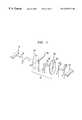
- FIGS. 1-2a first exemplary embodiment of a hybrid integrated wavelength selectable laser source and optical amplifier/modulator is schematically depicted in FIGS. 1-2.
- this hybrid integration approachadvantageously utilizes the well known optical bench technology to effect optical alignment and assembly between the different optical components. See, for example, U.S. Pat. Nos. 4,904,036; 4,210,923; and 4,989,935, which are incorporated herein by reference.
- Hybrid integrated optical transmitter 100comprises a semiconductor laser array 105 , optical combiner 110 , and optical amplifier/modulator 115 , which are all mechanically supported on and affixed to a platform 120 , such as a Beo or copper platform.
- a platform 120such as a Beo or copper platform.
- group III-V or II-VI semiconductorsmay be used, such as InGaAs/InGasP or InGaAsP/InP.
- a lensed fiber 125may be used to couple to the egressing radiation from optical amplifier/modulator 115 .
- Lensed fiber 125is positioned and aligned to optical amplifier/modulator 115 using properly dimensioned ferrules 130 and 135 , or using, for example, UV cured expoxy.
- Laser array 105may be any of the well known GaAlAs or InGaAsP/InP laser array structures.
- laser array 105may include distributed Bragg reflector (DBR) lasers, or distributed feedback (DFB) lasers.
- DBRdistributed Bragg reflector
- DFBdistributed feedback
- MFLsmultiple frequency lasers
- tunable lasersor any other form having a controlled emission wavelength may be used.
- optical amplifier/modulator 115Interposed between optical combiner 110 and optical amplifier/modulator 115 is an optical isolator 140 .
- Optical amplifier/modulator 115comprises optical amplifier 141 , preferably integrated with optical modulator 142 .
- Optical amplifier 141amplifies and optical modulator 142 then modulates optical radiation egressing from laser array 105 at wavelengths greater than ⁇ s , With the optical modulator positioned after first combining the radiation wavelengths of each laser in the array, the transmitter package requires only one high speed drive while still maintaining access to all wavelength channels.
- FIGS. 3-5illustrative depictions of the polarization states of the propagating light are depicted in FIGS. 3-5. The polarization states for both propagating and counter-propagating radiation are shown.
- optical isolator 140here consisting of a single 45° Faraday rotator 145 , which is preferably slightly tilted a few degrees to minimize back reflections into the laser. If the incident radiation is TE polarized, upon traversing through Faraday rotator 145 the light is rotated 45°.
- Unwanted radiation reflected from the end facet of the optical modulator after passing back through the Faraday rotatoris again rotated 45°. Although the unwanted reflection is not extinguished, it is TM polarized or orthogonal to the polarization state of the egressing light. Inasmuch as wavelength selectable laser 105 is designed to provide gain exclusively for TE polarized light, the TM polarized reflections do not affect the operating characteristics of the laser source.
- an additional polarizer 143(shown in dashed lines) having a transmission axis co-parallel (TE) with the polarization state of the incident radiation may be positioned in front of Faraday rotator 145 to totally extinguish the TM polarized back reflections.
- TEtransmission axis co-parallel
- optical isolator 140may consist of Faraday rotator 145 and a half-wave plate 150 oriented at 22.5° with respect to the vertical axis.
- the polarization states of the propagating lightare depicted in FIG. 4 .
- TE polarized light traversing through Faraday rotator 145 and half-wave plate 150maintains its polarization state, but reflected light from the optical modulator after traversing back through optical isolator 140 is now orthogonally rotated or TM polarized.
- optical amplifier 115is polarization sensitive and as such, half-wave plate 150 is used to properly orient the polarization state of the egressing radiation so as to be coupled into the optical amplifier/modulator.
- TE polarizer 143may be positioned in front of Faraday rotator 145 to totally extinguish the TM polarized back reflections.
- optical isolator 140may consist of Faraday rotator 145 and a polarizer 150 ′ having its transmission axis oriented at 45° with respect to the vertical axis.
- incident radiation after traversing through optical isolator 140is polarized 45° with respect to the incident radiation.
- Unwanted reflections that propagate back through the optical isolatorare rotated likewise 45° or TM polarized.
- TE polarizer 143may be positioned in front of Faraday rotator 145 to extinguish the back reflections, if desired.
- laser array 105comprising here of six (6) fixed frequency DFB lasers, L 1 -L 6 , operate at respectively different wavelengths ⁇ 1 - ⁇ 6 .
- Optical combiner 110fabricated with six (6) input waveguides, W 1 -W 6 , combines the different wavelengths from each corresponding laser within array 105 into a single output, W out .
- optical combiner 110utilizes a slab waveguide region wherein the different wavelength radiations each diffracts in the plane of the substrate to equally illuminate the output.
- Suitable structures for optical combiner 115are disclosed in the article by C. Dragone, “Efficient N ⁇ N Star Couplers Using Fourier Optics,” IEEE Journal of Lightwave Tech. Vol.
- optical combiner 110may alternatively use well known Y-branch tree structures, or other suitable branching waveguide structures.
- Standard fabrication techniquesare used to monolithically integrate laser array 105 and optical combiner 110 onto a single substrate S 1 , preferably an InP substrate.
- Optical combiner 110may be fabricated on a separate substrate and then positioned on platform 120 adjacent to laser array 105 .
- the active portions of the lasersare preferably mounted “junction down,” as described, for example, in Y. Seiwa et al., “High Power CW Operating over 400 mW on Five-Stripe Phase-Locked Laser Arrays Assembled By New Junction Down Mounting,” Journal of Applied Physics, Vol. 61, pp. 440-42 (1987).
- Fabrication techniques for integrating the individual elements of hybrid optical transmitter 100may be adapted from those techniques appearing in the article by Thomas L. Koch et al., entitled “Semiconductor Photonic Integrated Circuits,” IEEE J. Quantum Electron., Vol. QE-27, pp. 641-53 (1991), and U.S. Pat. No. 5,288,659, which are incorporated herein by reference.
- the various optical componentsare precisely positioned relative to each other on platform 120 through the use of complementary features, such solder bumps, mechanical features or optical fiducial that are fabricated on, for example, optical platform 120 .
- complementary featuressuch solder bumps, mechanical features or optical fiducial that are fabricated on, for example, optical platform 120 .
- selective surface etching of grooves and railsmay be used to facilitate alignment to the laser active portion(s).
- An alternative to this grooves-rails approachis by means of V-groove surface features on submount S 2 .
- K. E. Petersen“Silicon as Mechanical Material,” Proceedings of the IEEE, Vol. 70 (1982), pp. 420-57 (1982).
- each component above the optical platformcan be fixed to the desired distance by mounting the component on pedestal(s), the thickness of which is controlled during the fabrication of the platform.
- metallic trace patternsmay be fabricated on optical platform 120 to electrically contact laser array 105 , and/or optical amplifier/modulator 115 .
- the optical componentscan either be epoxied or soldered to optical platform 120 so as to affix each component to the platform.
- alloy compositions of lead and tincan be used for soldering.
- Optical platform 120can comprise one or more submounts of copper, diamond, silicon, ceramic or the like.
- the material chosen for optical platform 120is dependent on the desired application with respect to mechanical, thermal and electrical considerations. Copper or BeO may be used as the optical platform, with laser array 105 mounted on a silicon optical submount S 2 .
- a silicon optical submountalso allows the mature IC manufacturing technology to be exploited in aligning the optical components to each other.
- the waveguide structures of the optical combinermay be fabricated using waveguide mesas formed by conventional photolithographic masking and etching techniques. Alternatively, buried waveguide structures may also be used. See, for example, T. L. Koch et al., “Semiconductor Photonic Integrated Circuits,” IEEE Journal of Quantum Electronics, Vol. 27, No. 3 (March 1991); and U. Koren et al., “Wavelength Division Multiplexing Light Sources with Integrated Quantum Well Tunable Lasers and Optical Amplifiers,” Appl. Phys. Lett. 54(21), (May 22, 1989).
- Optical amplifier/modulator 115may utilize an electroabsorption bulk modulator structure, as disclosed in the article by U. Koren et al., “Polarisation Insensitive Semiconductor Optical Amplifier With Integrated Electroabsorption Modulators,” Electron. Lett., Vol. 32, No. 2, pp. 111-12 (January 1996). Also, directional coupler modulators as well as Mach-Zehnder modulators may be used. In the former instance, such optical amplifier/modulators are polarization insensitive. Hence, egressing radiation from laser array 105 through optical isolator 140 , although polarization rotated, is still amplified and modulated by optical amplifier/modulator 115 .
- optical isolator 140preferably includes a half-wave plate positioned in front of the optical amplifier/modulator so as to properly orient the polarization state of the egressing radiation so as to be coupled into the optical amplifier.
- an output polarizerTE
- TEoutput polarizer
- Optical amplifier 141 and optical modulator 142are preferably monolithically integrated on a substrate S 3 , different than substrate, S 1 , on which laser array 105 is fabricated. In this manner, each optical component may be optimized independently with respect to performance without the problems of material compatibility, and then appropriately assembled on platform 120 .
- optical isolator 140disposed between optical combiner 110 and optical amplifier/modulator 115 .
- a 45° Faraday rotator 145preferably a latching Faraday rotator, and a half-wave plate 150 ′ may be employed to effect optical isolation between the laser(s) and the optical amplifier/modulator, as discussed herein above.
- an additional TE polarizer 143may be positioned in front of Faraday rotator 145 to totally extinguish any back reflections.
- the latching Faraday rotatoris preferably implemented using the structure disclosed in the article by V. J.
- Such latching Faraday rotatorsutilize the Faraday effect in rare earth iron garnets, such as (Bi x Tb 1 ⁇ x ) 3 (Fe y Ga 1 ⁇ y ) 5 O 12 , which advantageously have a relatively low saturation magnetization. Accordingly, permanent magnets are not needed to maintain the Faraday rotator in its saturated state.
- Such magnetless Faraday rotatorssubstantially reduce cost, size and complexity, and, hence, make the present hybrid integration attractive for numerous optical communication applications.
- microlensesmay be used to match the size of the egressing radiation to the dimensions of the optical amplifier/modulator.
- ball lenses 155 and 160 disposed therebetweenmay be used to realize this benefit.
- Pyramid-shaped pits fabricated on submount S 2can be used to hold the microlenses.
- beam expandersmay be used on the output waveguide W out of optical combiner 110 , as well as on the input of optical amplifier/modulator 115 .
- beam expandersare integrated on the same substrate as their corresponding optical component.
- tapered beam expander waveguidesmay be used as disclosed in U.S. Pat. No. 5,574,742, entitled “Tapered Beam Expander Waveguide Integrated With A Diode Laser.”
- Wavelength selectabilityis achieved by simply activating the desired laser within laser array 105 .
- An external signalmay be applied to the optical amplifier/modulator to appropriately modulate the desired wavelength radiation in a manner well known in the art.
- each lasermay be actuated on a time division basis.
- Optical amplifier/modulator 115then modulates each wavelength on a time division basis with corresponding signals specific to each wavelength.
- FIG. 6there is illustrated another embodiment of the present invention similar to that of FIGS. 1-2, except employing a temperature tuning scheme to adjust the lasing wavelengths of laser array 105 .
- Platform 120is disposed on a submount 165 , which in turn is disposed on a thermoelectric cooler 170 (TEC).
- Thermoelectric cooler 170serves to maintain the temperature of hybrid transmitter 100 at a nominal temperature, T, corresponding to predetermined operating wavelengths.
- Excellent temperature controlmay be realized using a thermistor 175 disposed on submount 165 in a feedback configuration with thermoelectric cooler 170 .
- the wavelength of the egressing radiationcan be fine tuned by varying the temperature of the transmitter package, since changes in temperature cause corresponding variations in the refractive index of the active medium and hence changes in the effective length of the laser cavity.
- heating or coolingmay be applied locally and selectively only to the laser array.
- a resistive heater 180such as a chromium heater strip, may be disposed on laser array 105 to control the temperature of the active medium, thereby allowing the operating point of the laser array to be rapidly switched from one wavelength to another. While the use of a localized heater is beneficial for rapid switching, in operation such a localized heater offsets the effective heat load to thermoelectric cooler 170 . As such, it is contemplated that a compensating heater 185 disposed on optical submount 165 be used to keep constant the total heat load to the thermoelectric cooler. This may be expressed mathematically as follows:
- ⁇ lis the heat output of the localized heater
- ⁇ DEis the heat input of the thermoelectric cooler
- ⁇ cis the heat output of the compensating heater
- the intensity of the optical radiation from the laser arrayshould be maintained within a predetermined range. It is contemplated that this may be accomplished by diverting some of the optical radiation from the laser array to a monitoring photodetector which measures the average power egressing therefrom.
- the photodetectorsuch as a p-i-n photodidode, may be coupled to the output waveguide W out of optical combiner 110 so as to generate a signal which may be applied to a feedback circuit in order to adjust the laser bias current.
- This photodetectormay be integrated on substrate S 1 with the optical combiner or fabricated on a different substrate and positioned on platform 120 in a hybrid manner. In the former case, suitable fabrication techniques may be adapted as appearing in U.S. Pat. No. 5,288,659, entitled “Photonic-Integrated Circuit Fabrication Process,” which is incorporated herein by reference.
- Such feedback controlis beneficial, if not necessary, to compensate for environmental variations, such as temperature variations or performance degradations.
- wavelength monitoring photonicssuch as spectrometers
- the wavelength monitoring devicemay be fabricated on a separate substrate and appropriately placed on platform 120 or integrated with laser array 105 . In either case, suitable feedback controls well known in the art may be employed to correct for any deviations, such as by adjusting the temperature of the laser array.
- a InP DFB laser array and InP optical amplifier/modulator fabricated on individual photonic integrated circuit (PIC) chipsare packaged in a conventional “14-pin butterfly” laser package. Each chip is mounted on a copper submount, which in turn is mounted on a thermoelectric cooler (TEC) inside the butterfly package.
- the InP laser arrayconsisted of six ⁇ /4 shifted DFB InP lasers, each thermally tunable over eight (50 GHz) WDM channels. Because of the partial overlapping of the tunability ranges, only 32 channels can be accessed.
- a thin film ceramic 50 ⁇ resistor(500 ⁇ 500 ⁇ m area) is disposed on the laser array to effect localized thermal tuning, as discussed herein above.
- a matched compensating 50 ⁇ resistoris placed a similar distance from a monitoring thermistor to keep a constant heat load output, thereby preventing any temperature drift during channel switching. Due to the small thermal mass of the laser array and the thermal resistor, the thermal tuning is faster than that achieved using a conventional thermoelectric cooler (TEC). Indeed, experimental measurements indicate that for a 0.2 nm channel spectral window, the switching time for a 90% turn-on of a new channel is about 160 msec.
- TECthermoelectric cooler
- the laser arrayis fabricated on the same InP chip with a passive waveguide combiner feeding the laser output into a single mode waveguide.
- the output waveguideis coupled through a collimating ball lens to an optical isolator consisting of a latching 45° garnet Faraday rotator disposed between a TE polarizer and ⁇ /2 waveplate.
- the total thickness for the optical isolatoris only 850 ⁇ m: 200 ⁇ m for the TE polarizer, 500 ⁇ m for the Faraday rotator and 150 ⁇ m for the waveplate.
- Collimated light egressing from the optical isolatoris TE polarized and is then focused onto the amplifier/modulator chip using an aspheric micro-lens. Any unwanted reflections from the optical amplifier/modulator, are orthogonally polarized (TM), by the Faraday rotator and ⁇ /2 waveplate, and hence do not propagate through the TE polarizer.
- TMorthogonally polarized
- a fiberwas cleaved and directly butt coupled to the front facet of the optical amplifier/modulator.
- the input facet of the optical amplifier/modulatoris AR coated with a SiO thin film.
- a TiO 2 AR coatingis applied to minimize reflections between the optical amplifier/modulator and the output fiber.
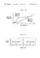
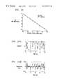
- FIG. 7Shown in FIG. 7 is the light output versus amplifier bias current characteristics for five of the six lasers. Each laser is biased at 60 mA and held nominally at a temperature of 15° C. It is believed that the ripple in the so-called L-I curves is caused by ripple in the amplifier gain spectrum, and unrelated to any mode hopping or instability in the lasers. This latter amplifier ripple is about 2 dB and may be improved by better AR coatings as well as higher optical power injection into the amplifier. Photocurrent measurements indicate that the optical power coupled into the optical amplifier is about ⁇ 12 to ⁇ 8 dBm. The wavelength spectra, with and without the laser turned “on,” are shown in FIGS. 8 and 9, respectively, indicating a better than 40 dB optical signal-to-noise ratio.
- FIG. 10Shown in FIG. 10 is the wavelength tuning characteristics of the above hybrid optical transmitter for each of the six lasers biased at 100 mA, and with the optical amplifier biased at 150 mA. Moreover, these measurements were taken with the temperature nominally set at 15° C. and then the tunning resistor biased with constant voltage steps of 0.2 volts. Shown in FIG. 11 is the associated plot of the optical frequency versus tuning resistor voltage for the six lasers. During these measurements, the compensating resistor is biased to provide a constant heat load of 1.15 W on the thermoelectric cooler. The first three wavelength spectra of laser number 1 and the last two spectra of laser number 6 , however, were taken with the temperature nominally set 11° C.
- FIGS. 13 (A)-(C)spectral linewidth measurements were made using different optical isolation configurations of the present invention, which measurements are illustrated in FIGS. 13 (A)-(C).
- FIG. 13Adepicts the spectral linewidth for a single illustrative laser measured under thermal tuning and employing an optical isolator consisting of a Faraday rotator disposed between a polarizer and ⁇ /2 waveplate, while in FIG. 13B the optical isolator consists of a Faraday rotator and ⁇ /2 waveplate. With the former configuration, an optical isolation of about 19 dB is observed.
- FIG. 13Cdepicts the tuning spectra obtained without the use of an optical isolator, showing large linewidth broadening for most of the tuned wavelengths.
- FIG. 13BAlthough some linewidth broadening is observed in FIG. 13B at the highest wavelength spectrum, none is observed in FIG. 13 A. This may be due to some interaction of the back reflected TM radiations with the MQW laser array, or perhaps due to the somewhat better optical isolation that can be obtained with the use of an additional TE polarizer positioned in front of the Faraday rotator that compensates for misalignment between the optical components in the optical isolator.
- FIGS. 14 (A)-(B)are illustrative eye diagrams for a single channel operating at a 2.5 Gb/s modulation, with a modulator Rf drive voltage of 2 volts peak-to-peak; laser bias current of 100 mA; and amplifier bias current of 150 mA.
- the modulator bias voltageis varied between 0.7 and 0.8 volts to show the trade off between “eye-opening” and “extinction ratio.” As seen in FIGS. 14 (A)-(B), although the former bias voltage provides a better “eye opening,” the latter provides a better “extinction ratio.”
- time-resolved wavelength measurementswere made to investigate the chirp of the hybrid optical transmitter. Such measurements indicate the chirp to substantially less than about 0.09 ⁇ .
- FIG. 15shown in FIG. 15 is another embodiment of the present invention similar to that of FIGS. 1-2, except utilizing a waveguide grating router multiple frequency laser (MFL) 105 ′ having a shared dispersive element disposed on a BeO ceramic platform 120 .
- MFLwaveguide grating router multiple frequency laser
- multiple frequency lasershave a relatively long cavity length. Because frequency wavelength shifts (chirp) induced by back reflected light is inversely proportional to the cavity length, multiple frequency lasers exhibit minimal chirp.
- Multiple frequency lasersare well known to those skilled the art and, hence, will not be discussed herein. A detailed discussion of multiple frequency lasers, however, can be found, for example, in the article by M.
- Two aspheric lenses 155 , 160couple the light from multiple frequency laser 105 ′ into a monothically integrated chip containing optical amplifier/modulator 115 .
- the optical amplifier/modulator designis polarization insensitive and is preferably oriented to couple light first into the optical amplifier which consists of alternating compressive and tensile strained quantum wells.
- Known fabrication techniquesare used to form the monolithically integrated chip, such as the technique described in the aforementioned article by U. Koren et al., “Polarisation Insensitive Semiconductor Optical Amplifier With Integrated Electroabsorption Modulators,” Electron Lett., Vol. 32, No. 2, pp. 111-12 (January 1996).
- the monolithically integrated amplifier/modulatorincludes a beam expander at the end facet of the modulator.
- a 45° latching Faraday rotator 145 and polarizer 150 ′are positioned between the two lenses.
- Polarizer 150 ′is oriented at 45° such that transverse electrically (TE) polarized light exiting multiple frequency laser 105 ′ propagates through optical isolator 140 .
- back reflected light from optical amplifier/modulator 115propagates through the optical isolator, but is rotated to be transverse magnetically (TM) polarized.
- Multiple frequency laser 105 ′includes intracavity amplifiers that provide gain exclusively for TE polarized light.
- multiple frequency laser 105 ′is substantially insensitive to TM polarized light and thus to the unwanted back reflections.
- an additional TE polarizermay be positioned in front of the Faraday rotator to totally extinguish the TM polarized back reflections.
- one main performance issueis the effect of optical feedback from the optical modulator into the multiple frequency laser.
- Such shared dispersive element type lasersachieve single mode stability from gain nonlinearities. Multimoding, which is necessarily accompanied by intensity fluctuations, is suppressed by power saturation in the optical amplifier portion of the laser. That is, higher intensity light receives less gain, thereby flattening any changes in intensity. Back reflections, however, into the laser cavity with the appropriate phase can cause an effective negative gain wherein higher intensity light receives more effective gain, as discussed below herein.
- G ( t )G ( t ⁇ )+ ⁇ G ( t ) (4)
- equation (3)may be approximated as
- the first term of equation (3)is the usual power saturation term responsible for suppressing intensity fluctuations that typically results from multimoding. As the intensity increases, the gain decreases.
- the second termis due, however, to the back reflection. Depending on its phase, the reflected light can act to reverse the gain such that the intensity increases as the gain decreases.
- the phase of the reflected lightis ⁇ II/2
- the magnitude of the negative gainis approximately a maximum since ⁇ is typically larger than unity. ⁇ This latter term becomes larger than the positive gain under the following condition:
- the normalized reflectivity R ext /R intshould be substantially less than 1/ ⁇ 2 .
- the normalized reflectivityshould be at least less than ⁇ 14 dB.
- FIG. 16depicts the light versus current curves (unregulated temperature) for hybrid optical transmitter 100 .
- Optical gainwas provided exclusively for TE polarized light.
- the multiple frequency laserhad a linewidth enhancement parameter, ⁇ , of about 5.2, with a cavity mode spacing of about 3.0 GHz.
- a distance of about 12 mmseparated the laser and optical amplifier/modulator.
- the laser drive currentwill be expressed as “array drive current, shared amplifier drive current,” whereas the drive to the optical amplifier/modulator will be expressed as “amplifier current, modulator bias voltage.”
- Laser Power(@ 50 mA, 50 mA) +3 dBm Coupling Loss (w/ isolation) ⁇ 3.6 dB Laser to Amplifier/Modulator Coupling Loss (w/o isolation) ⁇ 3.1 dB Laser to Amplifier/Modulator Power Coupled into Fiber +3.5 dBm Laser (@ 50 mA, 50 mA) Amplifier/Modulator (@ 75 mA, 0 V) Modulator/Amplifier 8.1 dB Compressed Gain Modulator/Amplifier 11.1 dB Uncompressed Gain
- the optical amplifier/modulator at a bias current of 75 mAexhibits a ripple, K, in its spontaneous emission spectrum of about 1 dB peak-to-peak.
- the average reflectivity of each end facet of the optical amplifier/modulatormay be determined from the following equation:
- the reflectivity of each end facet, R modis calculated to be about ⁇ 21.5 dB. Furthermore, the net reflectivity from the modulator facet back into the laser divided by the laser facet reflectivity is given by:
- multilongitudinal mode lasingis expected when the phase of the reflected light from the front end facet of the optical modulator is of the appropriate value.
- the relative intensity noise (RIN) and laser linewidthare ⁇ 141.0 dB/Hz and 910 kHz, respectively, for a positive gain phase.
- the RIN and laser linewdithare ⁇ 140.5 dB/Hz and 1.2 MHZ, respectively.
- These measurementswere made at a laser drive of 70 mA, 70 mA, and an amplifier/modulator drive of 75 mA, 0 V.
- the RIN and linewidthare 142 dB/Hz and 1.2 MHZ, respectively.
- FIGS. 17-18Shown in FIGS. 17-18 are exemplary wavelength spectra of the above hybrid wavelength selectable transmitter obtained through heterodyne detection. These spectra were obtained without optical isolator 140 . More specifically, radiation from the transmitter and an external cavity tunable laser tuned to a frequency 10 GHz therefrom were optically summed and displayed on a Rf spectrum analyzer.
- FIGS. 17 and 18illustrate the optical power spectra for the optical amplifier/modulator at bias currents of 79 and 51 mA, respectively. As evident from FIG. 17 (negative gain phase) and FIG. 18 (positive gain phase), the adjacent cavity modes are either enhanced or suppressed, depending on the phase of the reflected light. As expected for a phase dependent phenomenon, the side modes vary sinusoidally with the amplifier/modulator bias current, as expected in the absence of optical isolation.
- FIG. 20Shown in FIG. 20 is the optical spectra of all ten (10) channels of the transmitter obtained from experimental measurements. Importantly, the background optical power is nearly 50 dB below that of the lasing modes, despite the unwanted spontaneous emission added by the optical amplifier/modulator. Using a wavemeter, the average channel spacing is 199.8 GHz ⁇ 1.5 GHz.
- FIGS. 21-26depict design considerations for the above embodiment of the hybrid transmitter utilizing a multiple frequency laser. Unless otherwise indicated, the measurements were obtained using the following parameters: laser drive @ 70 mA, 70 mA; amplifier/modulator drive @ 75 mA, ⁇ 2.1 V; and modulator drive voltage @ 5 V peak-to-peak.
- FIG. 21Shown in FIG. 21 is the small-signal frequency characteristics of the optical modulator, indicating an electrical 3 dB bandwidth of about 4.2 GHz. Eye diagrams for all 10 channels are shown in FIG. 22 for a 2.5 Gb/s, 2 23 ⁇ 1 pseudo random pattern (using a 1.87 GHz bandwidth electronic filter). Because the optical modulator is made of bulk material, the optical bandwidth is broad. The extinction ratio, however is only about 7.5 dB. Specifically shown in FIG. 23 is an exemplary bit-error curve for channel 5 .
- FIGS. 24 (A)-(B)are the laser intensity and wavelength versus time plots, respectively, for the present hybrid optical transmitter without the use of the optical isolator.
- FIGS. 25 (A)-(B)depict the laser intensity and wavelength versus time plots, respectively, with the use of the optical isolator.
- back reflections from the optical modulatorcause small distortions in the intensity waveform as well as small wavelength perturbations. Indeed, when the lasing is multimode due to some back reflections, the intensity bit pattern becomes noisy.
- the chirpis substantially minimized and nearly identical for all ten channels, as further depicted in FIG. 26 .
Landscapes
- Physics & Mathematics (AREA)
- Optics & Photonics (AREA)
- Electromagnetism (AREA)
- Engineering & Computer Science (AREA)
- Computer Networks & Wireless Communication (AREA)
- Signal Processing (AREA)
- Optical Modulation, Optical Deflection, Nonlinear Optics, Optical Demodulation, Optical Logic Elements (AREA)
- Semiconductor Lasers (AREA)
Abstract
Description

| Parameters | Value | |||
| Laser Power (@ 50 mA, 50 mA) | +3 | dBm | ||
| Coupling Loss (w/ isolation) | −3.6 | dB | ||
| Laser to Amplifier/Modulator | ||||
| Coupling Loss (w/o isolation) | −3.1 | dB | ||
| Laser to Amplifier/Modulator | ||||
| Power Coupled into Fiber | +3.5 | dBm | ||
| Laser (@ 50 mA, 50 mA) | ||||
| Amplifier/Modulator (@ 75 mA, 0 V) | ||||
| Modulator/Amplifier | 8.1 | dB | ||
| Compressed Gain | ||||
| Modulator/Amplifier | 11.1 | dB | ||
| Uncompressed Gain | ||||

Claims (48)
Priority Applications (1)
| Application Number | Priority Date | Filing Date | Title |
|---|---|---|---|
| US09/038,269US6275317B1 (en) | 1998-03-10 | 1998-03-10 | Hybrid integration of a wavelength selectable laser source and optical amplifier/modulator |
Applications Claiming Priority (1)
| Application Number | Priority Date | Filing Date | Title |
|---|---|---|---|
| US09/038,269US6275317B1 (en) | 1998-03-10 | 1998-03-10 | Hybrid integration of a wavelength selectable laser source and optical amplifier/modulator |
Publications (1)
| Publication Number | Publication Date |
|---|---|
| US6275317B1true US6275317B1 (en) | 2001-08-14 |
Family
ID=21898983
Family Applications (1)
| Application Number | Title | Priority Date | Filing Date |
|---|---|---|---|
| US09/038,269Expired - LifetimeUS6275317B1 (en) | 1998-03-10 | 1998-03-10 | Hybrid integration of a wavelength selectable laser source and optical amplifier/modulator |
Country Status (1)
| Country | Link |
|---|---|
| US (1) | US6275317B1 (en) |
Cited By (92)
| Publication number | Priority date | Publication date | Assignee | Title |
|---|---|---|---|---|
| US20020085594A1 (en)* | 2000-10-30 | 2002-07-04 | Bardia Pezeshki | Tunable controlled laser array |
| US20020090011A1 (en)* | 2000-10-30 | 2002-07-11 | Bardia Pezeshki | Laser thermal tuning |
| US20020154666A1 (en)* | 2001-03-30 | 2002-10-24 | Vail Edward C. | Alignment of an on chip modulator |
| US20020154376A1 (en)* | 2001-03-30 | 2002-10-24 | Vail Edward C. | Modulator alignment for laser |
| US20020183002A1 (en)* | 2001-03-30 | 2002-12-05 | Vail Edward C. | Switched laser array modulation with integral electroabsorption modulator |
| US6516017B1 (en)* | 1999-11-11 | 2003-02-04 | Mitsubishi Denki Kabushiki Kaisha | Multiwavelength semiconductor laser device with single modulator and drive method therefor |
| US20030030919A1 (en)* | 2001-08-08 | 2003-02-13 | Bardia Pezeshki | Method and system for selecting an output of a VCSEL array |
| US20030039275A1 (en)* | 2001-08-08 | 2003-02-27 | Bardia Pezeshki | Method and system for selecting an output of a DBR array |
| WO2002101426A3 (en)* | 2001-03-09 | 2003-03-06 | Axon Photonics Inc | Multi-function semiconductor optical amplifier |
| US20030095736A1 (en)* | 2001-10-09 | 2003-05-22 | Kish Fred A. | Transmitter photonic integrated circuit (TxPIC) chip architectures and drive systems and wavelength stabilization for TxPICs |
| US20030095737A1 (en)* | 2001-10-09 | 2003-05-22 | Welch David F. | Transmitter photonic integrated circuits (TxPIC) and optical transport networks employing TxPICs |
| US20030099425A1 (en)* | 2001-11-06 | 2003-05-29 | Grubb Stephen G. | Optical communication module with one or more photonic integrated circuit (PIC) chips and an external booster optical amplifier for photonic integrated circuits (PICs) |
| KR20030062111A (en)* | 2002-01-16 | 2003-07-23 | 한국전자통신연구원 | Laser device, method for manufacturing the same and wavelength division multiplex light source |
| US6614955B1 (en)* | 2000-08-22 | 2003-09-02 | Agilent Technologies, Inc. | Method and apparatus for an extended wavelength range coherent optical spectrum analyzer |
| US20030185483A1 (en)* | 2002-03-27 | 2003-10-02 | Bennett Kevin W. | Optical monitoring and access module |
| US20030185486A1 (en)* | 2002-03-27 | 2003-10-02 | Bennett Kevin W. | Optical amplification module |
| US20030185518A1 (en)* | 2002-03-27 | 2003-10-02 | Bennett Kevin W. | Customer interface module |
| US20030184846A1 (en)* | 2002-03-27 | 2003-10-02 | Bennett Kevin W. | Modular optical amplifier assembly and a method of assembly |
| US20030185485A1 (en)* | 2002-03-27 | 2003-10-02 | Bennett Kevin W. | Optical processing module |
| US20030223683A1 (en)* | 2002-03-27 | 2003-12-04 | Bennett Kevin W. | Modular optical amplifier assembly |
| US20040001717A1 (en)* | 2002-03-27 | 2004-01-01 | Bennett Kevin W. | Optical power supply module |
| US20040013431A1 (en)* | 2002-04-01 | 2004-01-22 | Ed Vail | Laser and laser signal combiner |
| US20040017602A1 (en)* | 2002-03-27 | 2004-01-29 | Bennett Kevin W. | Modular optical amplifier assembly with self identifying modules |
| US6690686B2 (en)* | 1998-05-15 | 2004-02-10 | University Of Central Florida | Method for reducing amplitude noise in multi-wavelength modelocked semiconductor lasers |
| US20040028323A1 (en)* | 2002-03-27 | 2004-02-12 | Bennett Kevin W | Telemetry add/drop module |
| US6717733B2 (en)* | 2001-12-28 | 2004-04-06 | Nippon Sheet Glass Co., Ltd. | Collimator array |
| US20040096141A1 (en)* | 2002-11-18 | 2004-05-20 | Harmeet Singh | Optical multiplexer |
| US20040100635A1 (en)* | 2002-11-26 | 2004-05-27 | Intel Corporation | Coarse spectrometer with a grating |
| US20040101319A1 (en)* | 2002-11-26 | 2004-05-27 | Choi Kwang Seong | Wavelength stabilization module having light-receiving element array and method of manufacturing the same |
| US6771855B2 (en) | 2000-10-30 | 2004-08-03 | Santur Corporation | Laser and fiber coupling control |
| EP1457798A1 (en)* | 2003-03-12 | 2004-09-15 | Agilent Technologies, Inc. - a Delaware corporation - | Hybrid integrated optical module |
| US20040190580A1 (en)* | 2003-03-04 | 2004-09-30 | Bardia Pezeshki | High-yield high-precision distributed feedback laser based on an array |
| US6801551B1 (en)* | 1998-05-15 | 2004-10-05 | University Of Central Florida | Programmable multiwavelength modelocked laser |
| US20040223692A1 (en)* | 2003-04-01 | 2004-11-11 | Agilent Technologies, Inc. | Mounting arrangement for optical components |
| EP1492208A2 (en)* | 2003-06-27 | 2004-12-29 | NEC Corporation | Semiconductor laser module and method of assembling the same |
| US20050168826A1 (en)* | 2004-02-02 | 2005-08-04 | Serguei Koulikov | Method and apparatus for adjusting the path of an optical beam |
| US20050244994A1 (en)* | 2004-04-29 | 2005-11-03 | Agilent Technologies, Inc. | Wide tuneable laser sources |
| US20050276615A1 (en)* | 2004-06-15 | 2005-12-15 | Ranganath Tirumala R | Electroabsorption-modulated fabry-perot laser and methods of making the same |
| US20060051103A1 (en)* | 2004-09-08 | 2006-03-09 | Ranganath Tirumala R | Multi-channel fabry-perot laser transmitters and methods of generating multiple modulated optical signals |
| US7027469B2 (en) | 2001-11-30 | 2006-04-11 | Optitune Plc | Tunable filter |
| US7079718B2 (en) | 2001-10-09 | 2006-07-18 | Infinera Corporation | Optical probe and method of testing employing an interrogation beam or optical pickup |
| EP1696529A1 (en)* | 2005-02-28 | 2006-08-30 | Nettest France | Device for wide range continuous wavelength sweeping on a set of tunable laser sources |
| US7269354B1 (en)* | 2002-10-23 | 2007-09-11 | Lockheed Martin Corporation | Superheterodyne photonic receiver using non-serial frequency translation |
| US20080031626A1 (en)* | 2001-10-09 | 2008-02-07 | Infinera Corporation | Photonic Integrated Circuit (PIC) Chips |
| US20080044128A1 (en)* | 2001-10-09 | 2008-02-21 | Infinera Corporation | TRANSMITTER PHOTONIC INTEGRATED CIRCUITS (TxPICs) AND OPTICAL TRANSPORT NETWORK SYSTEM EMPLOYING TxPICs |
| WO2008059281A1 (en)* | 2006-11-18 | 2008-05-22 | The Centre For Integrated Photonics Limited | Multiwavelength transmitter |
| US20080131141A1 (en)* | 2006-11-30 | 2008-06-05 | Ranganath Tirumala R | Parallel channel optical communication using modulator array and shared laser |
| US20080138088A1 (en)* | 2001-10-09 | 2008-06-12 | Infinera Corporation | Monolithic transmitter photonic integrated circuit (txpic) having tunable modulated sources with feedback system for source power level or wavelength tuning |
| US20090021835A1 (en)* | 2002-10-08 | 2009-01-22 | Infinera Corporation | TILTED COMBINERS/DECOMBINERS AND PHOTONIC INTEGRATED CIRCUITS (PICs) EMPLOYING THE SAME |
| US7522836B2 (en) | 2001-02-02 | 2009-04-21 | Cheetah Omni, Llc | Optical logic gate based optical router |
| US7573928B1 (en) | 2003-09-05 | 2009-08-11 | Santur Corporation | Semiconductor distributed feedback (DFB) laser array with integrated attenuator |
| WO2009105374A1 (en)* | 2008-02-19 | 2009-08-27 | Lockheed Martin Coherent Technologies, Inc. | Phase and polarization controlled beam combining devices and methods |
| US20090219960A1 (en)* | 2008-02-19 | 2009-09-03 | Lockheed Martin Coherent Technologies, Inc. | Phase and polarization controlled beam combining devices and methods |
| US20090307614A1 (en)* | 2008-06-06 | 2009-12-10 | Apple Inc. | Media content and chat integration |
| US20100020832A1 (en)* | 2008-07-23 | 2010-01-28 | U.S.Government as represented by the Secretary of the Army | Wavelength selectable laser systems and related methods |
| US20110038635A1 (en)* | 2009-08-14 | 2011-02-17 | Futurewei Technologies, Inc. | Colorless Dense Wavelength Division Multiplexing Transmitters |
| US20110235667A1 (en)* | 2010-03-25 | 2011-09-29 | Sumitomo Electric Industries, Ltd. | Semiconductor laser |
| US20110235659A1 (en)* | 2010-03-25 | 2011-09-29 | Sumitomo Electric Industries, Ltd. | Semiconductor laser |
| US20110261439A1 (en)* | 2008-11-04 | 2011-10-27 | Forschungsverbund Berlin E.V. | Device and Method for Selective Transmission of an Optical Signal |
| US20120163821A1 (en)* | 2010-12-22 | 2012-06-28 | Electronics And Telecommunications Research Institute | Multi-wavelength optical source generator |
| US20120281723A1 (en)* | 2011-05-06 | 2012-11-08 | Electronics And Telecommunications Research Institute | Wavelength-tunable external cavity laser |
| US20130094074A1 (en)* | 2011-10-14 | 2013-04-18 | Mehdi Asghari | Gain medium providing laser and amplifier functionality to optical device |
| US20130208350A1 (en)* | 2012-02-15 | 2013-08-15 | Mitsubishi Electric Corporation | Optical semiconductor device |
| JP2014075554A (en)* | 2012-10-05 | 2014-04-24 | Fujitsu Ltd | Variable wavelength light source and wavelength variable method |
| EP2637266A4 (en)* | 2010-12-14 | 2014-05-07 | Huawei Tech Co Ltd | External cavity laser and wavelength division multiplexing passive optical network system |
| US20140140087A1 (en)* | 2011-05-04 | 2014-05-22 | James I. Scholtz | Multiple wavelength light source and signal collection device and methods for using the same |
| US20140306131A1 (en)* | 2008-07-09 | 2014-10-16 | Luxtera, Inc. | Light source assembly supporting direct coupling to an integrated circuit |
| US20150049379A1 (en)* | 2010-12-29 | 2015-02-19 | Alcatel-Lucent Usa, Inc. | Optical amplifier for multi-core optical fiber |
| WO2015157351A1 (en)* | 2014-04-09 | 2015-10-15 | Robin Huang | Integrated wavelength beam combining laser systems |
| US20150358085A1 (en)* | 2014-06-05 | 2015-12-10 | Xilinx, Inc. | Optical communication circuits |
| WO2016149607A1 (en)* | 2015-03-18 | 2016-09-22 | Applied Optoelectronics, Inc. | Tunable laser including parallel lasing cavities with a common output |
| JP2017005034A (en)* | 2015-06-05 | 2017-01-05 | 日本電信電話株式会社 | Wavelength tunable laser array and wavelength tunable laser array wavelength control method |
| JP2017037971A (en)* | 2015-08-10 | 2017-02-16 | 日本電信電話株式会社 | Narrow linewidth tunable semiconductor laser |
| US20170075188A1 (en)* | 2015-04-03 | 2017-03-16 | Sumitomo Osaka Cement Co., Ltd. | Optical waveguide device |
| US9804330B1 (en)* | 2016-06-28 | 2017-10-31 | Mitsubishi Electric Corporation | Semiconductor device |
| CN107820575A (en)* | 2015-04-01 | 2018-03-20 | 甲骨文国际公司 | Integrated laser with back-reflecting isolator |
| WO2018110172A1 (en)* | 2016-12-16 | 2018-06-21 | 住友電気工業株式会社 | Optical module |
| US10084285B1 (en) | 2017-08-28 | 2018-09-25 | Hewlett Packard Enterprise Development Lp | Orthoganolly polarized VCSELs |
| US10177872B1 (en) | 2017-09-25 | 2019-01-08 | Hewlett Packard Enterprise Development Lp | Orthogonally polarized VCSELs |
| US20190157841A1 (en)* | 2016-08-22 | 2019-05-23 | Morton Photonics, Inc. | Ultra-low noise, highly stable single-mode operation, high power, bragg grating based semiconductor laser |
| US10511400B2 (en)* | 2018-01-22 | 2019-12-17 | Electronics And Telecommunications Research Institute | Optical multiplexer for multiplexing optical signals using optical waveguide block including laminated layers |
| US20200052460A1 (en)* | 2016-10-18 | 2020-02-13 | Optella Inc. | Optical module |
| CN111929776A (en)* | 2019-05-22 | 2020-11-13 | 祥茂光电科技股份有限公司 | Temperature-control multi-channel optical emission subassembly and transceiver module comprising same |
| US20210281044A1 (en)* | 2020-01-02 | 2021-09-09 | Institute Of Semiconductors, Chinese Academy Of Sciences | Broadband tuning system and method |
| CN113381283A (en)* | 2021-06-11 | 2021-09-10 | 福州市纳飞光电科技有限公司 | Compact pulse laser amplifier |
| US20220107229A1 (en)* | 2020-10-05 | 2022-04-07 | Juniper Networks, Inc. | Optical temperature measurements in photonic circuits |
| US11402576B2 (en)* | 2020-04-16 | 2022-08-02 | Quintessent Inc. | Passive compensation of non-uniform channel characteristics of spectrally selective device arrays in multiwavelength photonic integrated circuits |
| US20220407286A1 (en)* | 2019-03-21 | 2022-12-22 | JeongSoo Kim | Optical device capable of precise adjustment of optical output intensity, and method for manufacturing optical device |
| WO2022267542A1 (en)* | 2021-06-21 | 2022-12-29 | 华为技术有限公司 | Transmission method for service optical signal, and network device and optical network |
| US11557789B2 (en) | 2017-11-02 | 2023-01-17 | Imec Vzw | Solid electrolyte, electrode, power storage device, and method for producing solid electrolytes |
| US11699810B2 (en) | 2017-04-24 | 2023-07-11 | Imec Vzw | Solid nanocomposite electrolyte materials |
| US11710850B2 (en) | 2017-11-02 | 2023-07-25 | Imec Vzw | Solid electrolyte, electrode, power storage device, and method for producing solid electrolytes |
Citations (14)
| Publication number | Priority date | Publication date | Assignee | Title |
|---|---|---|---|---|
| US4210923A (en) | 1979-01-02 | 1980-07-01 | Bell Telephone Laboratories, Incorporated | Edge illuminated photodetector with optical fiber alignment |
| US4904036A (en) | 1988-03-03 | 1990-02-27 | American Telephone And Telegraph Company, At&T Bell Laboratories | Subassemblies for optoelectronic hybrid integrated circuits |
| US4989935A (en) | 1988-09-30 | 1991-02-05 | Siemens Aktiengesellschaft | Optoelectronic transmitter and receiver |
| US5134671A (en) | 1990-08-03 | 1992-07-28 | At&T Bell Laboratories | Monolithic integrated optical amplifier and photodetector |
| US5288659A (en) | 1988-08-26 | 1994-02-22 | At&T Bell Laboratories | Photonic-integrated-circuit fabrication process |
| US5373385A (en)* | 1993-11-12 | 1994-12-13 | At&T Corp. | Method and apparatus for reduction of optical communication system impairments |
| US5394489A (en) | 1993-07-27 | 1995-02-28 | At&T Corp. | Wavelength division multiplexed optical communication transmitters |
| US5444725A (en) | 1994-09-30 | 1995-08-22 | At&T Ipm Corp. | Multifrequency laser |
| US5479544A (en)* | 1992-10-03 | 1995-12-26 | Canon Kabushiki Kaisha | Optical receiver, optical semiconductor apparatus, and optical communication system utilizing the same |
| US5568303A (en)* | 1994-06-30 | 1996-10-22 | U.S. Philips Corporation | Unit for generating signal pulses, transmitter comprising such a unit, and multiplex transmission system comprising such a transmitter |
| US5574742A (en) | 1994-05-31 | 1996-11-12 | Lucent Technologies Inc. | Tapered beam expander waveguide integrated with a diode laser |
| US5576881A (en) | 1995-08-29 | 1996-11-19 | Lucent Technologies Inc. | Multi-frequency optical signal source having reduced distortion and crosstalk |
| US5608570A (en) | 1995-07-05 | 1997-03-04 | Lucent Technologies Inc. | Article comprising a magneto-optic material having low magnetic moment |
| US5642447A (en)* | 1994-12-21 | 1997-06-24 | E-Tek Dynamics, Inc. | Fiber optic network transmission system with integrated optical isolator couplers |
- 1998
- 1998-03-10USUS09/038,269patent/US6275317B1/ennot_activeExpired - Lifetime
Patent Citations (14)
| Publication number | Priority date | Publication date | Assignee | Title |
|---|---|---|---|---|
| US4210923A (en) | 1979-01-02 | 1980-07-01 | Bell Telephone Laboratories, Incorporated | Edge illuminated photodetector with optical fiber alignment |
| US4904036A (en) | 1988-03-03 | 1990-02-27 | American Telephone And Telegraph Company, At&T Bell Laboratories | Subassemblies for optoelectronic hybrid integrated circuits |
| US5288659A (en) | 1988-08-26 | 1994-02-22 | At&T Bell Laboratories | Photonic-integrated-circuit fabrication process |
| US4989935A (en) | 1988-09-30 | 1991-02-05 | Siemens Aktiengesellschaft | Optoelectronic transmitter and receiver |
| US5134671A (en) | 1990-08-03 | 1992-07-28 | At&T Bell Laboratories | Monolithic integrated optical amplifier and photodetector |
| US5479544A (en)* | 1992-10-03 | 1995-12-26 | Canon Kabushiki Kaisha | Optical receiver, optical semiconductor apparatus, and optical communication system utilizing the same |
| US5394489A (en) | 1993-07-27 | 1995-02-28 | At&T Corp. | Wavelength division multiplexed optical communication transmitters |
| US5373385A (en)* | 1993-11-12 | 1994-12-13 | At&T Corp. | Method and apparatus for reduction of optical communication system impairments |
| US5574742A (en) | 1994-05-31 | 1996-11-12 | Lucent Technologies Inc. | Tapered beam expander waveguide integrated with a diode laser |
| US5568303A (en)* | 1994-06-30 | 1996-10-22 | U.S. Philips Corporation | Unit for generating signal pulses, transmitter comprising such a unit, and multiplex transmission system comprising such a transmitter |
| US5444725A (en) | 1994-09-30 | 1995-08-22 | At&T Ipm Corp. | Multifrequency laser |
| US5642447A (en)* | 1994-12-21 | 1997-06-24 | E-Tek Dynamics, Inc. | Fiber optic network transmission system with integrated optical isolator couplers |
| US5608570A (en) | 1995-07-05 | 1997-03-04 | Lucent Technologies Inc. | Article comprising a magneto-optic material having low magnetic moment |
| US5576881A (en) | 1995-08-29 | 1996-11-19 | Lucent Technologies Inc. | Multi-frequency optical signal source having reduced distortion and crosstalk |
Non-Patent Citations (11)
| Title |
|---|
| C. Dragone, "Efficient N x N Star Couplers Using Fourier Optics," Journal Of Lightwave Technology, vol. 7, No. 3, Mar. 1989, pp. 479-489. |
| Ippen et al., "Additive Pulse Mode Locking," J. Opt. Soc. Am. B/vol. 6, No. 9, Sep. 1989, pp. 1736-1745. |
| J.M. Verdiell et al., "8-Wavelength DBR Laser Array Fabricated with a Single-Step Bragg Grating Printing Technique," IEEE Photonics Technology Letters, vol. 5, No. 6, Jun. 1993, pp. 619-621. |
| Joyner et al., "An 8-Channel Digitally Tunable Transmitter with Electroabsorption Modulated Output by Selective-Area Epitaxy," IEEE Photonics Technology Letters, vol. 7, No. 9, Sep. 1995, pp. 1013-1015. |
| Koren et al., "Polarisation Insensitive Semiconductor Optical Amplifier With Integrated Electroabsorption Modulators," Electronics Letters, 18th Jan. 1996, vol. 32, No. 2, pp. 111-112. |
| Kurt E. Petersen, "Silicon as a Mechanical Material," Proceedings Of The IEEE, vol. 70, No. 5, May 1982, pp. 420-457. |
| Takeuchi et al., "Low-Loss Single-Mode GaAs/A1GaAs Miniature Optical Waveguides with Straight and Bending Structures," Journal Of Lightwave Technology, vol. 7, No. 7, Jul. 1989, pp. 1044-1054. |
| U. Koren et al., "Wavelength Division Multiplexing Light Source With Integrated Quantum Well Tunable Lasers And Optical Amplifiers," Appl. Phys. Lett. 54(21) May 22, 1989, pp. 2056-2058. |
| Y. Seiwa et al., "High Power CW Operation over 400 mW On Five-Stripe Phase-Locked Laser Arrays Assembled By New Junction Down Mounting," J. Appl. Phys. 61(1), Jan. 1, 1987, pp. 440-442. |
| Zirngibl et al., "Digitally Tunable Laser Based on the Integration of a Waveguide Grating Multiplexer and an Optical Amplifier," IEEE Photonics Technology Letters, vol. 6, No. 4, Apr. 1994, pp. 156-518. |
| Zirngibl et al., "Digitally Tunable Laser Based on the Integration of a Waveguide Grating Multiplexer and an Optical Amplifier," IEEE Photonics Technology Letters, vol. 6, No. 4, Apr. 1994, pp. 516-518. |
Cited By (208)
| Publication number | Priority date | Publication date | Assignee | Title |
|---|---|---|---|---|
| US6801551B1 (en)* | 1998-05-15 | 2004-10-05 | University Of Central Florida | Programmable multiwavelength modelocked laser |
| US6690686B2 (en)* | 1998-05-15 | 2004-02-10 | University Of Central Florida | Method for reducing amplitude noise in multi-wavelength modelocked semiconductor lasers |
| US6516017B1 (en)* | 1999-11-11 | 2003-02-04 | Mitsubishi Denki Kabushiki Kaisha | Multiwavelength semiconductor laser device with single modulator and drive method therefor |
| US6614955B1 (en)* | 2000-08-22 | 2003-09-02 | Agilent Technologies, Inc. | Method and apparatus for an extended wavelength range coherent optical spectrum analyzer |
| US20040213515A1 (en)* | 2000-10-30 | 2004-10-28 | Santur Corporation | Laser and fiber coupling control |
| US6795453B2 (en) | 2000-10-30 | 2004-09-21 | Santur Corporation | Laser thermal tuning |
| US6914916B2 (en) | 2000-10-30 | 2005-07-05 | Santur Corporation | Tunable controlled laser array |
| US6771855B2 (en) | 2000-10-30 | 2004-08-03 | Santur Corporation | Laser and fiber coupling control |
| US7382950B2 (en) | 2000-10-30 | 2008-06-03 | Santur Corporation | Laser and fiber coupling control |
| US7345802B2 (en) | 2000-10-30 | 2008-03-18 | Santur Corporation | Laser and fiber coupling control |
| US20020085594A1 (en)* | 2000-10-30 | 2002-07-04 | Bardia Pezeshki | Tunable controlled laser array |
| US20040228577A1 (en)* | 2000-10-30 | 2004-11-18 | Bardia Pezeshki | Laser and fiber coupling control |
| US20020090011A1 (en)* | 2000-10-30 | 2002-07-11 | Bardia Pezeshki | Laser thermal tuning |
| US7522836B2 (en) | 2001-02-02 | 2009-04-21 | Cheetah Omni, Llc | Optical logic gate based optical router |
| WO2002101426A3 (en)* | 2001-03-09 | 2003-03-06 | Axon Photonics Inc | Multi-function semiconductor optical amplifier |
| US6813300B2 (en)* | 2001-03-30 | 2004-11-02 | Santur Corporation | Alignment of an on chip modulator |
| US6922278B2 (en)* | 2001-03-30 | 2005-07-26 | Santur Corporation | Switched laser array modulation with integral electroabsorption modulator |
| US20020183002A1 (en)* | 2001-03-30 | 2002-12-05 | Vail Edward C. | Switched laser array modulation with integral electroabsorption modulator |
| US20020154376A1 (en)* | 2001-03-30 | 2002-10-24 | Vail Edward C. | Modulator alignment for laser |
| US6781734B2 (en) | 2001-03-30 | 2004-08-24 | Santur Corporation | Modulator alignment for laser |
| US20020154666A1 (en)* | 2001-03-30 | 2002-10-24 | Vail Edward C. | Alignment of an on chip modulator |
| US6879442B2 (en) | 2001-08-08 | 2005-04-12 | Santur Corporation | Method and system for selecting an output of a VCSEL array |
| US20030039275A1 (en)* | 2001-08-08 | 2003-02-27 | Bardia Pezeshki | Method and system for selecting an output of a DBR array |
| US20030030919A1 (en)* | 2001-08-08 | 2003-02-13 | Bardia Pezeshki | Method and system for selecting an output of a VCSEL array |
| US20080044128A1 (en)* | 2001-10-09 | 2008-02-21 | Infinera Corporation | TRANSMITTER PHOTONIC INTEGRATED CIRCUITS (TxPICs) AND OPTICAL TRANSPORT NETWORK SYSTEM EMPLOYING TxPICs |
| US7062114B2 (en) | 2001-10-09 | 2006-06-13 | Infinera Corporation | Submount for a photonic integrated circuit (PIC) chip |
| US7680368B2 (en) | 2001-10-09 | 2010-03-16 | Infinera Corporation | Monolithic transmitter photonic integrated circuit (TxPIC) with a traversely disposed output |
| US7672546B2 (en) | 2001-10-09 | 2010-03-02 | Infinera Corporation | Optical transport network having a plurality of monolithic photonic integrated circuit semiconductor chips |
| US20040067006A1 (en)* | 2001-10-09 | 2004-04-08 | Welch David F. | Transmitter photonic integrated circuit ( TxPIC) chips |
| US7751658B2 (en) | 2001-10-09 | 2010-07-06 | Infinera Corporation | Monolithic transmitter photonic integrated circuit (TxPIC) having tunable modulated sources with feedback system for source power level or wavelength tuning |
| US7792396B2 (en) | 2001-10-09 | 2010-09-07 | Infinera Corporation | Probe card for testing in-wafer photonic integrated circuits (PICs) and method of use |
| US20030095736A1 (en)* | 2001-10-09 | 2003-05-22 | Kish Fred A. | Transmitter photonic integrated circuit (TxPIC) chip architectures and drive systems and wavelength stabilization for TxPICs |
| US7519246B2 (en) | 2001-10-09 | 2009-04-14 | Infinera Corporation | Photonic integrated circuit (PIC) chips |
| US7489838B2 (en) | 2001-10-09 | 2009-02-10 | Infinera Corporation | Optical transmitter |
| US7483599B2 (en) | 2001-10-09 | 2009-01-27 | Infinera Corporation | Method of calibrating a monolithic transmitter photonic integrated circuit (TXPIC) chip |
| US7477807B2 (en) | 2001-10-09 | 2009-01-13 | Infinera Corporation | Monolithic transmitter photonic integrated circuit (TxPIC) semiconductor chip |
| US7885492B2 (en) | 2001-10-09 | 2011-02-08 | Infinera Corporation | Transmitter photonic integrated circuit (TxPIC) chips |
| US20080138088A1 (en)* | 2001-10-09 | 2008-06-12 | Infinera Corporation | Monolithic transmitter photonic integrated circuit (txpic) having tunable modulated sources with feedback system for source power level or wavelength tuning |
| US7460742B2 (en) | 2001-10-09 | 2008-12-02 | Infinera Corporation | Method and apparatus for providing an antireflection coating on the output facet of a photonic integrated circuit (PIC) chip |
| US20030095737A1 (en)* | 2001-10-09 | 2003-05-22 | Welch David F. | Transmitter photonic integrated circuits (TxPIC) and optical transport networks employing TxPICs |
| US9971090B2 (en) | 2001-10-09 | 2018-05-15 | Infinera Corporation | Apparatus and method for tuning a laser source emission wavelength employing a laser source contact comprising electrode segments |
| US20030099018A1 (en)* | 2001-10-09 | 2003-05-29 | Jagdeep Singh | Digital optical network architecture |
| US20080031626A1 (en)* | 2001-10-09 | 2008-02-07 | Infinera Corporation | Photonic Integrated Circuit (PIC) Chips |
| US7324719B2 (en) | 2001-10-09 | 2008-01-29 | Infinera Corporation | Method tuning optical components integrated in a monolithic photonic integrated circuit (PIC) |
| US7295783B2 (en) | 2001-10-09 | 2007-11-13 | Infinera Corporation | Digital optical network architecture |
| US20050013332A1 (en)* | 2001-10-09 | 2005-01-20 | Infinera Corporation | Method and apparatus of monitoring and controlling the emission wavelengths of a plurality of laser sources integrated on the same chip or in the same photonic integrated circuit (PIC) |
| US20050018720A1 (en)* | 2001-10-09 | 2005-01-27 | Infinera Corporation | Contact length trimming or vernier resistor trimming of a semiconductor laser source contact to change the source applied current density and resulting operational wavelength |
| US20050025409A1 (en)* | 2001-10-09 | 2005-02-03 | Infinera Corporation | Submount for a photonic integrated circuit (PIC) chip |
| US20050063636A1 (en)* | 2001-10-09 | 2005-03-24 | Infinera Corporation | Method and apparatus for providing an antireflection coating on the output facet of a photonic integrated circuit (PIC) chip |
| US20070248299A1 (en)* | 2001-10-09 | 2007-10-25 | Infinera Corporation | Monolithic Transmitter Photonic Integrated Circuit (TxPIC) Semiconductor Chip |
| US20070242918A1 (en)* | 2001-10-09 | 2007-10-18 | Infinera Corporation | Transmitter Photonic Integrated Circuits (TxPICs) with Directly Modulated Lasers and Wavelength Selective Combiners |
| US20050094927A1 (en)* | 2001-10-09 | 2005-05-05 | Infinera Corporation | Probe card for testing in-wafer photonic integrated circuits (PICs) and method of use |
| US20050094925A1 (en)* | 2001-10-09 | 2005-05-05 | Infinera Corporation | Method of in-wafer testing of monolithic photonic integrated circuits (PICs) formed in a semiconductor wafer |
| US20050094926A1 (en)* | 2001-10-09 | 2005-05-05 | Infinera Corporation | Method of calibrating a monolithic transmitter photonic integrated circuit (TxPIC) chip |
| US20050100345A1 (en)* | 2001-10-09 | 2005-05-12 | Infinera Corporation | Monolithic transmitter/receiver photonic integrated circuit (Tx/RxPIC) transceiver chip |
| US7283694B2 (en)* | 2001-10-09 | 2007-10-16 | Infinera Corporation | Transmitter photonic integrated circuits (TxPIC) and optical transport networks employing TxPICs |
| US20070172169A1 (en)* | 2001-10-09 | 2007-07-26 | Infinera Corporation | Method of tuning optical components integrated in a monolithic photonic integrated circuit (pic) |
| US7200296B2 (en) | 2001-10-09 | 2007-04-03 | Infinera Corporation | Monolithic photonic integrated circuit (PIC) CHIP |
| US20070019901A1 (en)* | 2001-10-09 | 2007-01-25 | Infinera Corporation | Method tuning optical components integrated in a monolithic photonic integrated circuit (PIC) |
| US7136546B2 (en) | 2001-10-09 | 2006-11-14 | Infinera Corporation | Method and apparatus of monitoring and controlling the emission wavelengths of a plurality of laser sources integrated on the same chip or in the same photonic integrated circuit (PIC) |
| US7103239B2 (en) | 2001-10-09 | 2006-09-05 | Infinera Corporation | Optical transmitter |
| US7092589B2 (en) | 2001-10-09 | 2006-08-15 | Infinera Corporation | Method of tuning integrated laser sources with integrated wavelength tuning elements on the same substrate or in a monolithic photonic integrated circuit (PIC) |
| US7079719B2 (en) | 2001-10-09 | 2006-07-18 | Infinera Corporation | Method of tuning optical components integrated on a monolithic chip |
| US7471857B2 (en) | 2001-10-09 | 2008-12-30 | Infinera Corporation | Method of tuning optical components integrated in a monolithic photonic integrated circuit (PIC) |
| US7079720B2 (en) | 2001-10-09 | 2006-07-18 | Infinera Corporation | Method of operating an array of laser sources integrated in a monolithic chip or in a photonic integrated circuit (PIC) |
| US20050286909A1 (en)* | 2001-10-09 | 2005-12-29 | Infinera Corporation | Optical transmitter |
| US6985648B2 (en) | 2001-10-09 | 2006-01-10 | Infinera Corporation | Method of in-wafer testing of monolithic photonic integrated circuits (PICs) formed in a semiconductor wafer |
| US7079721B2 (en) | 2001-10-09 | 2006-07-18 | Infinera Corporation | Method and apparatus of monitoring and controlling the emission wavelengths of a plurality of laser sources integrated on the same chip or in the same photonic integrated circuit (PIC) |
| US20060023992A1 (en)* | 2001-10-09 | 2006-02-02 | Infinera Corporation | Method of in-wafer testing of monolithic photonic integrated circuits (PICs) formed in a semiconductor wafer |
| US7079715B2 (en) | 2001-10-09 | 2006-07-18 | Infinera Corporation | Transmitter photonic integrated circuit (TxPIC) chip architectures and drive systems and wavelength stabilization for TxPICs |
| US7079718B2 (en) | 2001-10-09 | 2006-07-18 | Infinera Corporation | Optical probe and method of testing employing an interrogation beam or optical pickup |
| US7466882B2 (en) | 2001-10-09 | 2008-12-16 | Infinera Corporation | Monolithic transmitter/receiver photonic integrated circuit (Tx/RxPIC) transceiver chip |
| US7043109B2 (en) | 2001-10-09 | 2006-05-09 | Infinera Corporation | Method of in-wafer testing of monolithic photonic integrated circuits (PICs) formed in a semiconductor wafer |
| US20060062519A1 (en)* | 2001-10-09 | 2006-03-23 | Infinera Corporation | Monolithic photonic integrated circuit (PIC) chip and a method tuning optical components integrated in a monolithic photonic integrated circuit (PIC) |
| US20050169640A1 (en)* | 2001-11-06 | 2005-08-04 | Infinera Corporation | Optical communication module having at least one monolithic semiconductor photonic integrated circuit chip |
| US20030099425A1 (en)* | 2001-11-06 | 2003-05-29 | Grubb Stephen G. | Optical communication module with one or more photonic integrated circuit (PIC) chips and an external booster optical amplifier for photonic integrated circuits (PICs) |
| US7058248B2 (en) | 2001-11-06 | 2006-06-06 | Infinera Corporation | Optical communication system with multiple photonic integrated circuit (PIC) chips and an external booster optical amplifier for photonic integrated circuits (PICs) |
| US20040247233A1 (en)* | 2001-11-06 | 2004-12-09 | Grubb Stephen G. | Method of providing a low cost semiconductor transmitter photonic integrated circuit (TxPIC) chip |
| US7062111B2 (en) | 2001-11-06 | 2006-06-13 | Grubb Stephen G | Optical communication module with one or more photonic integrated circuit (PIC) chips and an external booster optical amplifier for photonic integrated circuits (PICs) |
| WO2003044913A3 (en)* | 2001-11-06 | 2003-10-30 | Infinera Corp | Optical communication module with photonic integrated circuit chip (pic) and external booster optical amplifier |
| US7010185B2 (en) | 2001-11-06 | 2006-03-07 | Infinera Corporation | Method of providing a low cost semiconductor transmitter photonic integrated circuit (TxPIC) chip |
| US7130499B2 (en) | 2001-11-06 | 2006-10-31 | Infinera Corporation | Optical communication module utilizing plural semiconductor transmitter photonic integrated circuit (TxPIC) chips |
| US7027469B2 (en) | 2001-11-30 | 2006-04-11 | Optitune Plc | Tunable filter |
| US6717733B2 (en)* | 2001-12-28 | 2004-04-06 | Nippon Sheet Glass Co., Ltd. | Collimator array |
| KR20030062111A (en)* | 2002-01-16 | 2003-07-23 | 한국전자통신연구원 | Laser device, method for manufacturing the same and wavelength division multiplex light source |
| US20030185485A1 (en)* | 2002-03-27 | 2003-10-02 | Bennett Kevin W. | Optical processing module |
| US20030185486A1 (en)* | 2002-03-27 | 2003-10-02 | Bennett Kevin W. | Optical amplification module |
| US20030185518A1 (en)* | 2002-03-27 | 2003-10-02 | Bennett Kevin W. | Customer interface module |
| US6937385B2 (en) | 2002-03-27 | 2005-08-30 | Avanex Corporation | Customer interface module |
| US20040001717A1 (en)* | 2002-03-27 | 2004-01-01 | Bennett Kevin W. | Optical power supply module |
| US20040017602A1 (en)* | 2002-03-27 | 2004-01-29 | Bennett Kevin W. | Modular optical amplifier assembly with self identifying modules |
| US20040028323A1 (en)* | 2002-03-27 | 2004-02-12 | Bennett Kevin W | Telemetry add/drop module |
| US6917731B2 (en) | 2002-03-27 | 2005-07-12 | Corning Incorporated | Optical amplification module |
| US20030185483A1 (en)* | 2002-03-27 | 2003-10-02 | Bennett Kevin W. | Optical monitoring and access module |
| US20030184846A1 (en)* | 2002-03-27 | 2003-10-02 | Bennett Kevin W. | Modular optical amplifier assembly and a method of assembly |
| US20030223683A1 (en)* | 2002-03-27 | 2003-12-04 | Bennett Kevin W. | Modular optical amplifier assembly |
| US6910780B2 (en) | 2002-04-01 | 2005-06-28 | Santur Corporation | Laser and laser signal combiner |
| US20050168819A1 (en)* | 2002-04-01 | 2005-08-04 | Santur Corporation | Laser and laser signal combiner |
| US20040013431A1 (en)* | 2002-04-01 | 2004-01-22 | Ed Vail | Laser and laser signal combiner |
| US7747114B2 (en) | 2002-10-08 | 2010-06-29 | Infinera Corporation | Tilted combiners/decombiners and photonic integrated circuits (PICs) employing the same |
| US20090021835A1 (en)* | 2002-10-08 | 2009-01-22 | Infinera Corporation | TILTED COMBINERS/DECOMBINERS AND PHOTONIC INTEGRATED CIRCUITS (PICs) EMPLOYING THE SAME |
| US7269354B1 (en)* | 2002-10-23 | 2007-09-11 | Lockheed Martin Corporation | Superheterodyne photonic receiver using non-serial frequency translation |
| US20080002933A1 (en)* | 2002-11-18 | 2008-01-03 | Jds Uniphase Corporation | Optical Multiplexer |
| US7366364B2 (en)* | 2002-11-18 | 2008-04-29 | Jds Uniphase Corporation | Optical multiplexer |
| US20040096141A1 (en)* | 2002-11-18 | 2004-05-20 | Harmeet Singh | Optical multiplexer |
| WO2004046764A3 (en)* | 2002-11-18 | 2005-04-14 | Optovia Corp | Optical multiplexer |
| US20040101319A1 (en)* | 2002-11-26 | 2004-05-27 | Choi Kwang Seong | Wavelength stabilization module having light-receiving element array and method of manufacturing the same |
| US20060050271A1 (en)* | 2002-11-26 | 2006-03-09 | Mcdonald Mark | Coarse spectrometer with a grating |
| US6993057B2 (en)* | 2002-11-26 | 2006-01-31 | Intel Corporation | Coarse spectrometer with a grating |
| US7012939B2 (en)* | 2002-11-26 | 2006-03-14 | Electronics And Telecommunications Research Institute | Wavelength stabilization module having light-receiving element array and method of manufacturing the same |
| US20060062271A1 (en)* | 2002-11-26 | 2006-03-23 | Mcdonald Mark | Coarse spectrometer with a grating |
| US7259904B2 (en) | 2002-11-26 | 2007-08-21 | Intel Corporation | Coarse spectrometer with a grating |
| US7333526B2 (en)* | 2002-11-26 | 2008-02-19 | Intel Corporation | Coarse spectrometer with a grating |
| US20040100635A1 (en)* | 2002-11-26 | 2004-05-27 | Intel Corporation | Coarse spectrometer with a grating |
| US20040190580A1 (en)* | 2003-03-04 | 2004-09-30 | Bardia Pezeshki | High-yield high-precision distributed feedback laser based on an array |
| EP1457798A1 (en)* | 2003-03-12 | 2004-09-15 | Agilent Technologies, Inc. - a Delaware corporation - | Hybrid integrated optical module |
| US7474826B2 (en)* | 2003-04-01 | 2009-01-06 | Avago Technologies General Ip (Singapore) Pte. Ltd. | Mounting arrangement for optical components |
| US20040223692A1 (en)* | 2003-04-01 | 2004-11-11 | Agilent Technologies, Inc. | Mounting arrangement for optical components |
| US7308012B2 (en)* | 2003-06-27 | 2007-12-11 | Nec Corporation | Semiconductor laser module and method of assembling the same |
| US20040264538A1 (en)* | 2003-06-27 | 2004-12-30 | Masahiko Namiwaka | Semiconductor laser module and method of assembling the same |
| EP1492208A2 (en)* | 2003-06-27 | 2004-12-29 | NEC Corporation | Semiconductor laser module and method of assembling the same |
| US7573928B1 (en) | 2003-09-05 | 2009-08-11 | Santur Corporation | Semiconductor distributed feedback (DFB) laser array with integrated attenuator |
| US20050168826A1 (en)* | 2004-02-02 | 2005-08-04 | Serguei Koulikov | Method and apparatus for adjusting the path of an optical beam |
| US7424041B2 (en)* | 2004-04-29 | 2008-09-09 | Avago Technologies Fiber Ip Pte Ltd. | Wide tuneable laser sources |
| US20050244994A1 (en)* | 2004-04-29 | 2005-11-03 | Agilent Technologies, Inc. | Wide tuneable laser sources |
| US7502567B2 (en) | 2004-06-15 | 2009-03-10 | Avago Technologies Fiber Ip (Singapore) Pte. Ltd. | Electroabsorption-modulated Fabry-Perot laser and methods of making the same |
| US20050276615A1 (en)* | 2004-06-15 | 2005-12-15 | Ranganath Tirumala R | Electroabsorption-modulated fabry-perot laser and methods of making the same |
| US7747174B2 (en) | 2004-09-08 | 2010-06-29 | Avago Technologies Fiber Ip (Singapore) Pte. Ltd. | Multi-channel fabry-perot laser transmitters and methods of generating multiple modulated optical signals |
| US20060051103A1 (en)* | 2004-09-08 | 2006-03-09 | Ranganath Tirumala R | Multi-channel fabry-perot laser transmitters and methods of generating multiple modulated optical signals |
| US20080267230A1 (en)* | 2005-02-28 | 2008-10-30 | Anritsu Instruments Sas | Device For Wide Range Continuous Wavelength Sweeping on a Set of Tunable Laser Sources |
| EP1696529A1 (en)* | 2005-02-28 | 2006-08-30 | Nettest France | Device for wide range continuous wavelength sweeping on a set of tunable laser sources |
| WO2006089802A1 (en)* | 2005-02-28 | 2006-08-31 | Anritsu Instruments Sas | Device for wide range continuous wavelength sweeping on a set of tunable laser sources |
| US20100142962A1 (en)* | 2006-11-18 | 2010-06-10 | Poustie Alistair J | Multiwavelength transmitter |
| US8326154B2 (en) | 2006-11-18 | 2012-12-04 | Huawei Technologies Co., Ltd. | Multiwavelength transmitter |
| WO2008059281A1 (en)* | 2006-11-18 | 2008-05-22 | The Centre For Integrated Photonics Limited | Multiwavelength transmitter |
| US20080131141A1 (en)* | 2006-11-30 | 2008-06-05 | Ranganath Tirumala R | Parallel channel optical communication using modulator array and shared laser |
| US7734189B2 (en) | 2006-11-30 | 2010-06-08 | Avago Technologies Fiber Ip (Singapore) Pte. Ltd. | Parallel channel optical communication using modulator array and shared laser |
| US20090219960A1 (en)* | 2008-02-19 | 2009-09-03 | Lockheed Martin Coherent Technologies, Inc. | Phase and polarization controlled beam combining devices and methods |
| WO2009105374A1 (en)* | 2008-02-19 | 2009-08-27 | Lockheed Martin Coherent Technologies, Inc. | Phase and polarization controlled beam combining devices and methods |
| US7817688B2 (en) | 2008-02-19 | 2010-10-19 | Lockheed Martin Coherent Technologies, Inc. | Phase and polarization controlled beam combining devices and methods |
| US20090307614A1 (en)* | 2008-06-06 | 2009-12-10 | Apple Inc. | Media content and chat integration |
| US10234646B2 (en)* | 2008-07-09 | 2019-03-19 | Luxtera, Inc. | Light source assembly supporting direct coupling to an integrated circuit |
| US20140306131A1 (en)* | 2008-07-09 | 2014-10-16 | Luxtera, Inc. | Light source assembly supporting direct coupling to an integrated circuit |
| US20100020832A1 (en)* | 2008-07-23 | 2010-01-28 | U.S.Government as represented by the Secretary of the Army | Wavelength selectable laser systems and related methods |
| US8315283B2 (en) | 2008-07-23 | 2012-11-20 | The United States Of America As Represented By The Secretary Of The Army | Wavelength selectable laser systems and related methods |
| US20110261439A1 (en)* | 2008-11-04 | 2011-10-27 | Forschungsverbund Berlin E.V. | Device and Method for Selective Transmission of an Optical Signal |
| US8559098B2 (en)* | 2008-11-04 | 2013-10-15 | Forschungsverbund Berlin E.V. | Device and method for selective transmission of an optical signal |
| US20110038635A1 (en)* | 2009-08-14 | 2011-02-17 | Futurewei Technologies, Inc. | Colorless Dense Wavelength Division Multiplexing Transmitters |
| US8417118B2 (en)* | 2009-08-14 | 2013-04-09 | Futurewei Technologies, Inc. | Colorless dense wavelength division multiplexing transmitters |
| US20110235667A1 (en)* | 2010-03-25 | 2011-09-29 | Sumitomo Electric Industries, Ltd. | Semiconductor laser |
| US8488637B2 (en)* | 2010-03-25 | 2013-07-16 | Sumitomo Electric Industries Ltd. | Semiconductor laser |
| US20110235659A1 (en)* | 2010-03-25 | 2011-09-29 | Sumitomo Electric Industries, Ltd. | Semiconductor laser |
| US8737446B2 (en) | 2010-03-25 | 2014-05-27 | Sumitomo Electric Industries, Ltd. | Semiconductor laser |
| EP2637266A4 (en)* | 2010-12-14 | 2014-05-07 | Huawei Tech Co Ltd | External cavity laser and wavelength division multiplexing passive optical network system |
| US20120163821A1 (en)* | 2010-12-22 | 2012-06-28 | Electronics And Telecommunications Research Institute | Multi-wavelength optical source generator |
| US8644714B2 (en)* | 2010-12-22 | 2014-02-04 | Electronics And Telecommunications Research Institute | Multi-wavelength optical source generator |
| US20150049379A1 (en)* | 2010-12-29 | 2015-02-19 | Alcatel-Lucent Usa, Inc. | Optical amplifier for multi-core optical fiber |
| US9103987B2 (en)* | 2010-12-29 | 2015-08-11 | Alcatel Lucent | Optical amplifier for multi-core optical fiber |
| US9423548B2 (en)* | 2011-05-04 | 2016-08-23 | The Research Foundation Of The City University Of New York | Multiple wavelength light source and signal collection device and methods for using the same |
| US20140140087A1 (en)* | 2011-05-04 | 2014-05-22 | James I. Scholtz | Multiple wavelength light source and signal collection device and methods for using the same |
| US20120281723A1 (en)* | 2011-05-06 | 2012-11-08 | Electronics And Telecommunications Research Institute | Wavelength-tunable external cavity laser |
| US9025241B2 (en)* | 2011-10-14 | 2015-05-05 | Kotura, Inc. | Gain medium providing laser and amplifier functionality to optical device |
| US20130094074A1 (en)* | 2011-10-14 | 2013-04-18 | Mehdi Asghari | Gain medium providing laser and amplifier functionality to optical device |
| US9042008B2 (en) | 2012-02-15 | 2015-05-26 | Mitsubishi Electric Corporation | Optical semiconductor device |
| US20150229407A1 (en)* | 2012-02-15 | 2015-08-13 | Mitsubishi Electric Corporation | Optical semiconductor device |
| US9147997B2 (en)* | 2012-02-15 | 2015-09-29 | Mitsubishi Electric Corporation | Optical semiconductor device |
| US20130208350A1 (en)* | 2012-02-15 | 2013-08-15 | Mitsubishi Electric Corporation | Optical semiconductor device |
| JP2014075554A (en)* | 2012-10-05 | 2014-04-24 | Fujitsu Ltd | Variable wavelength light source and wavelength variable method |
| WO2015157351A1 (en)* | 2014-04-09 | 2015-10-15 | Robin Huang | Integrated wavelength beam combining laser systems |
| US20150358085A1 (en)* | 2014-06-05 | 2015-12-10 | Xilinx, Inc. | Optical communication circuits |
| US9520949B2 (en)* | 2014-06-05 | 2016-12-13 | Xilinx, Inc. | Optical communication circuits |
| US10014949B1 (en) | 2014-06-05 | 2018-07-03 | Xilinx, Inc. | Optical communication circuits |
| WO2016149607A1 (en)* | 2015-03-18 | 2016-09-22 | Applied Optoelectronics, Inc. | Tunable laser including parallel lasing cavities with a common output |
| US9768585B2 (en) | 2015-03-18 | 2017-09-19 | Applied Optoelectronics, Inc. | Tunable laser including parallel lasing cavities with a common output |
| JP2018513556A (en)* | 2015-04-01 | 2018-05-24 | オラクル・インターナショナル・コーポレイション | Integrated laser with back-reflective isolator |
| CN107820575A (en)* | 2015-04-01 | 2018-03-20 | 甲骨文国际公司 | Integrated laser with back-reflecting isolator |
| US9935424B2 (en)* | 2015-04-01 | 2018-04-03 | Oracle International Corporation | Integrated laser with back-reflection isolator |
| US20170075188A1 (en)* | 2015-04-03 | 2017-03-16 | Sumitomo Osaka Cement Co., Ltd. | Optical waveguide device |
| US10365534B2 (en)* | 2015-04-03 | 2019-07-30 | Sumitmo Osaka Cement Co., Ltd. | Optical waveguide device |
| JP2017005034A (en)* | 2015-06-05 | 2017-01-05 | 日本電信電話株式会社 | Wavelength tunable laser array and wavelength tunable laser array wavelength control method |
| JP2017037971A (en)* | 2015-08-10 | 2017-02-16 | 日本電信電話株式会社 | Narrow linewidth tunable semiconductor laser |
| US9804330B1 (en)* | 2016-06-28 | 2017-10-31 | Mitsubishi Electric Corporation | Semiconductor device |
| US20190157841A1 (en)* | 2016-08-22 | 2019-05-23 | Morton Photonics, Inc. | Ultra-low noise, highly stable single-mode operation, high power, bragg grating based semiconductor laser |
| US10476233B2 (en)* | 2016-08-22 | 2019-11-12 | Morton Photonics, Inc. | Ultra-low noise, highly stable single-mode operation, high power, Bragg grating based semiconductor laser |
| US10483718B2 (en) | 2016-08-22 | 2019-11-19 | Morton Photonics, Inc. | Ultra-low noise, highly stable single-mode operation, high power, Bragg grating based semiconductor laser |
| US20200052460A1 (en)* | 2016-10-18 | 2020-02-13 | Optella Inc. | Optical module |
| WO2018110172A1 (en)* | 2016-12-16 | 2018-06-21 | 住友電気工業株式会社 | Optical module |
| US20190237932A1 (en)* | 2016-12-16 | 2019-08-01 | Sumitomo Electric Industries, Ltd. | Optical module |
| JPWO2018110172A1 (en)* | 2016-12-16 | 2019-10-24 | 住友電気工業株式会社 | Optical module |
| US10601200B2 (en)* | 2016-12-16 | 2020-03-24 | Sumitomo Electric Industries, Ltd. | Optical module |
| US11699810B2 (en) | 2017-04-24 | 2023-07-11 | Imec Vzw | Solid nanocomposite electrolyte materials |
| US10084285B1 (en) | 2017-08-28 | 2018-09-25 | Hewlett Packard Enterprise Development Lp | Orthoganolly polarized VCSELs |
| US10177872B1 (en) | 2017-09-25 | 2019-01-08 | Hewlett Packard Enterprise Development Lp | Orthogonally polarized VCSELs |
| US11710850B2 (en) | 2017-11-02 | 2023-07-25 | Imec Vzw | Solid electrolyte, electrode, power storage device, and method for producing solid electrolytes |
| US11557789B2 (en) | 2017-11-02 | 2023-01-17 | Imec Vzw | Solid electrolyte, electrode, power storage device, and method for producing solid electrolytes |
| US10511400B2 (en)* | 2018-01-22 | 2019-12-17 | Electronics And Telecommunications Research Institute | Optical multiplexer for multiplexing optical signals using optical waveguide block including laminated layers |
| US20220407286A1 (en)* | 2019-03-21 | 2022-12-22 | JeongSoo Kim | Optical device capable of precise adjustment of optical output intensity, and method for manufacturing optical device |
| US12401172B2 (en)* | 2019-03-21 | 2025-08-26 | JeongSoo Kim | Optical device capable of precise adjustment of optical output intensity, and method for manufacturing optical device |
| US11146039B2 (en)* | 2019-05-22 | 2021-10-12 | Applied Optoelectronics, Inc. | Temperature controlled multi-channel transmitter optical subassembly and transceiver module including same |
| CN111929776B (en)* | 2019-05-22 | 2023-08-11 | 祥茂光电科技股份有限公司 | Temperature control multi-channel light emission subassembly and transceiver module comprising same |
| CN111929776A (en)* | 2019-05-22 | 2020-11-13 | 祥茂光电科技股份有限公司 | Temperature-control multi-channel optical emission subassembly and transceiver module comprising same |
| US20210281044A1 (en)* | 2020-01-02 | 2021-09-09 | Institute Of Semiconductors, Chinese Academy Of Sciences | Broadband tuning system and method |
| US11876347B2 (en)* | 2020-01-02 | 2024-01-16 | Institute Of Semiconductors, Chinese Academy Of Sciences | Broadband tuning system and method |
| US11402576B2 (en)* | 2020-04-16 | 2022-08-02 | Quintessent Inc. | Passive compensation of non-uniform channel characteristics of spectrally selective device arrays in multiwavelength photonic integrated circuits |
| US20220107229A1 (en)* | 2020-10-05 | 2022-04-07 | Juniper Networks, Inc. | Optical temperature measurements in photonic circuits |
| US11698308B2 (en)* | 2020-10-05 | 2023-07-11 | Openlight Photonics, Inc. | Optical temperature measurements in photonic circuits |
| CN113381283A (en)* | 2021-06-11 | 2021-09-10 | 福州市纳飞光电科技有限公司 | Compact pulse laser amplifier |
| WO2022267542A1 (en)* | 2021-06-21 | 2022-12-29 | 华为技术有限公司 | Transmission method for service optical signal, and network device and optical network |
Similar Documents
| Publication | Publication Date | Title |
|---|---|---|
| US6275317B1 (en) | Hybrid integration of a wavelength selectable laser source and optical amplifier/modulator | |
| CN118763500B (en) | Wavelength control method for silicon photonic external cavity tunable laser | |
| Zhou et al. | A widely tunable narrow linewidth semiconductor fiber ring laser | |
| US5870417A (en) | Thermal compensators for waveguide DBR laser sources | |
| US6862136B2 (en) | Hybrid optical transmitter with electroabsorption modulator and semiconductor optical amplifier | |
| Franz et al. | Optical Communications: Components and Systems: Analysis--design--optimization--application | |
| US4914667A (en) | Hybrid laser for optical communications, and transmitter, system, and method | |
| US6845121B2 (en) | Optical isolator apparatus and methods | |
| US20050018732A1 (en) | Uncooled and high temperature long reach transmitters, and high power short reach transmitters | |
| US8073337B2 (en) | Optical clock recovery apparatus and method and birefringent medium | |
| Tsang | The cleaved-couple-cavity (C3) laser | |
| JP4860608B2 (en) | Electroabsorption modulated Fabry-Perot laser and method of manufacturing the same | |
| US4638483A (en) | High speed intensity modulated light source | |
| US20020186730A1 (en) | Integrated multiple wavelength pump laser module | |
| US7747174B2 (en) | Multi-channel fabry-perot laser transmitters and methods of generating multiple modulated optical signals | |
| JPS61168980A (en) | Semiconductor light-emitting element | |
| Ohyama et al. | Transmitter optical subassembly using a polarization beam combiner for 100 Gbit/s Ethernet over 40-km transmission | |
| Marshall et al. | Optical system with two packaged 1.5 μm semiconductor laser amplifier repeaters | |
| Dreyer et al. | High-gain mode-adapted semiconductor optical amplifier with 12.4-dBm saturation output power at 1550 nm | |
| TOHMORI et al. | Wavelength Tunable 1.5 µm GaInAsP/InP Bundle-Integrated-Guide Distributed Bragg Reflector (BIG-DBR) Lasers | |
| EP3903146B1 (en) | Interferometric enhancement of an electroabsorptive modulated laser | |
| Shu et al. | Tunable dual-wavelength picosecond optical pulses generated from a self-injection seeded gain-switched laser diode | |
| Grillanda et al. | 16 wavelengths comb source using large-scale hybrid photonic integration | |
| Doerr et al. | Characterization of the hybrid integration of a shared dispersive element laser and a modulator | |
| Kapsalis et al. | Tunable wavelength conversion using cross-gain modulation in a vertically coupled microring laser |
Legal Events
| Date | Code | Title | Description |
|---|---|---|---|
| AS | Assignment | Owner name:LUCENT TECHNOLOGIES, INC., NEW JERSEY Free format text:ASSIGNMENT OF ASSIGNORS INTEREST;ASSIGNORS:DOERR, CHRISTOPHER R.;JOHNSON, JOHN E.;JOYNER, CHARLES H.;AND OTHERS;REEL/FRAME:009068/0061;SIGNING DATES FROM 19980220 TO 19980305 | |
| AS | Assignment | Owner name:AGERE SYSTEMS OPTOELECTRONICS GUARDIAN CORP., FLOR Free format text:ASSIGNMENT OF ASSIGNORS INTEREST;ASSIGNOR:LUCENT TECHNOLOGIES INC.;REEL/FRAME:011908/0492 Effective date:20010130 | |
| STCF | Information on status: patent grant | Free format text:PATENTED CASE | |
| FEPP | Fee payment procedure | Free format text:PAYOR NUMBER ASSIGNED (ORIGINAL EVENT CODE: ASPN); ENTITY STATUS OF PATENT OWNER: LARGE ENTITY Free format text:PAYER NUMBER DE-ASSIGNED (ORIGINAL EVENT CODE: RMPN); ENTITY STATUS OF PATENT OWNER: LARGE ENTITY | |
| FPAY | Fee payment | Year of fee payment:4 | |
| FPAY | Fee payment | Year of fee payment:8 | |
| FPAY | Fee payment | Year of fee payment:12 | |
| AS | Assignment | Owner name:DEUTSCHE BANK AG NEW YORK BRANCH, AS COLLATERAL AG Free format text:PATENT SECURITY AGREEMENT;ASSIGNORS:LSI CORPORATION;AGERE SYSTEMS LLC;REEL/FRAME:032856/0031 Effective date:20140506 | |
| AS | Assignment | Owner name:AVAGO TECHNOLOGIES GENERAL IP (SINGAPORE) PTE. LTD Free format text:ASSIGNMENT OF ASSIGNORS INTEREST;ASSIGNOR:AGERE SYSTEMS LLC;REEL/FRAME:035365/0634 Effective date:20140804 | |
| AS | Assignment | Owner name:AGERE SYSTEMS LLC, PENNSYLVANIA Free format text:TERMINATION AND RELEASE OF SECURITY INTEREST IN PATENT RIGHTS (RELEASES RF 032856-0031);ASSIGNOR:DEUTSCHE BANK AG NEW YORK BRANCH, AS COLLATERAL AGENT;REEL/FRAME:037684/0039 Effective date:20160201 Owner name:LSI CORPORATION, CALIFORNIA Free format text:TERMINATION AND RELEASE OF SECURITY INTEREST IN PATENT RIGHTS (RELEASES RF 032856-0031);ASSIGNOR:DEUTSCHE BANK AG NEW YORK BRANCH, AS COLLATERAL AGENT;REEL/FRAME:037684/0039 Effective date:20160201 | |
| AS | Assignment | Owner name:BANK OF AMERICA, N.A., AS COLLATERAL AGENT, NORTH CAROLINA Free format text:PATENT SECURITY AGREEMENT;ASSIGNOR:AVAGO TECHNOLOGIES GENERAL IP (SINGAPORE) PTE. LTD.;REEL/FRAME:037808/0001 Effective date:20160201 Owner name:BANK OF AMERICA, N.A., AS COLLATERAL AGENT, NORTH Free format text:PATENT SECURITY AGREEMENT;ASSIGNOR:AVAGO TECHNOLOGIES GENERAL IP (SINGAPORE) PTE. LTD.;REEL/FRAME:037808/0001 Effective date:20160201 | |
| AS | Assignment | Owner name:AVAGO TECHNOLOGIES GENERAL IP (SINGAPORE) PTE. LTD., SINGAPORE Free format text:TERMINATION AND RELEASE OF SECURITY INTEREST IN PATENTS;ASSIGNOR:BANK OF AMERICA, N.A., AS COLLATERAL AGENT;REEL/FRAME:041710/0001 Effective date:20170119 Owner name:AVAGO TECHNOLOGIES GENERAL IP (SINGAPORE) PTE. LTD Free format text:TERMINATION AND RELEASE OF SECURITY INTEREST IN PATENTS;ASSIGNOR:BANK OF AMERICA, N.A., AS COLLATERAL AGENT;REEL/FRAME:041710/0001 Effective date:20170119 |